ANALOG DEVICES AD9856 Service Manual
CMOS 200 MHz
www.BDTIC.com/ADI
FEATURES
Universal low cost modulator solution for communications
applications
DC to 80 MHz output bandwidth
Integrated 12-bit D/A converter
Programmable sample rate interpolation filter
Programmable reference clock multiplier
Internal SIN(x)/x compensation filter
>52 dB SFDR @ 40 MHz A
>48 dB SFDR @ 70 MHz A
>80 dB narrow-band SFDR @ 70 MHz A
+3 V single-supply operation
Space-saving surface-mount packaging
Bidirectional control bus interface
Supports burst and continuous Tx modes
Single-tone mode for frequency synthesis applications
Four programmable, pin-selectable, modulator profiles
Direct interface to AD8320/AD8321 PGA cable driver
OUT
OUT
OUT
Quadrature Digital Upconverter
AD9856
APPLICATIONS
HFC data, telephony, and video modems
Wireless and satellite communications
Cellular base stations
GENERAL DESCRIPTION
The AD9856 integrates a high speed, direct digital synthesizer
(DDS), a high performance, high speed, 12-bit digital-to-analog
converter (DAC), clock multiplier circuitry, digital filters, and
other DSP functions on a single chip to form a complete
quadrature digital upconverter device. The AD9856 is intended
to function as a universal I/Q modulator and agile upconverter
for communications applications where cost, size, power
dissipation, and dynamic performance are critical attributes.
The AD9856 is available in a space-saving surface-mount
package, and is specified to operate over the extended industrial
temperature range of −40°C to +85°C.
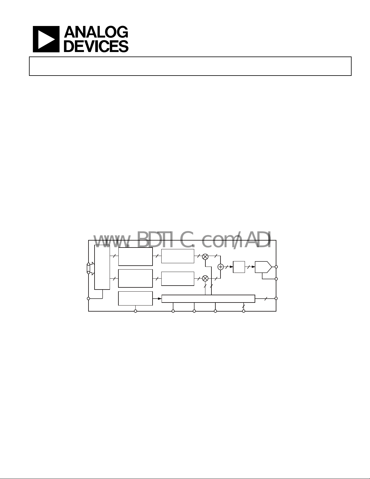
FUNCTIONAL BLOCK DIAGRAM
AD9856
12
12
INV
SINC
BIDIRECTIONAL SPI CONTROL INTERFACE:
32-BIT FREQUENCY TUNING WORD
FREQUENCY UPDATE
INTERPOLATION FILTER RATE
REFERENCE CLOCK MULTIPLIER RATE
SPECTRAL PHASE INVERSION ENABLE
CABLE DRIVER AMPLIFIER CONTROL
12-BIT
DAC
DC-80 MHz
OUTPUT
DAC
R
SET
SPI INTERFACE
TO AD8320/AD8321
PROGRAMMABLE
CABLE DRIVER
AMPLIFIER
00637-C-001
COMPLEX
DATA IN
TxENABLE
(I/Q SYNC)
4 × TO 8 ×
12
SELECTABLE
INTERPOLATING
HALFBANDS
4 × TO 8 ×
12
SELECTABLE
CONVERTER
INTERPOLATING
DEMULTIPLEXER AND
SERIAL-TO-PARALLEL
HALFBANDS
4 × TO 20 × PROG.
CLOCK
MULTIPLIER
REFERENCE
CLOCK IN
12
2 × TO 63 ×
SELECTABLE
INTERPOLATOR
2 × TO 63 ×
12
SELECTABLE
INTERPOLATOR
DDS AND CONTROL FUNCTIONS
1–2
PROFILE
SELECT
PROFILE
SELECT
3–4
12
12
12
12
1212
COSINESINE
MASTER
RESET
Figure 1.
Rev. C
Information furnished by Analog Devices is believed to be accurate and reliable.
However, no responsibility is assumed by Analog Devices for its use, nor for any
infringements of patents or other rights of third parties that may result from its use.
Specifications subject to change without notice. No license is granted by implication
or otherwise under any patent or patent rights of Analog Devices. Trademarks and
registered trademarks are the property of their respective owners.
One Technology Way, P.O. Box 9106, Norwood, MA 02062-9106, U.S.A.
Tel: 781.329.4700 www.analog.com
Fax: 781.326.8703 © 2005 Analog Devices, Inc. All rights reserved.

AD9856
www.BDTIC.com/ADI
TABLE OF CONTENTS
Specifications..................................................................................... 3
Digital Quadrature Modulator ................................................. 23
Absolute Maximum Ratings............................................................ 5
Explanation of Test Levels........................................................... 5
ESD Caution.................................................................................. 5
Pin Configuration and Function Descriptions............................. 6
Typical Performance Characteristics............................................. 8
Typical Modulated Output Spe ctral Plots .................................8
Typical Single-Tone Output Spectral Plots............................... 9
Typical Narrow-Band SFDR Spectral Plots ............................ 10
Typical Phase Noise Spectral Plots........................................... 10
Typical Plots of Output Constellations....................................11
Power Consumption .................................................................. 12
Serial Control Bus Register ...........................................................13
Register Bit Definitions.............................................................. 14
Theory of Operation ...................................................................... 15
Modulation Mode Operation ................................................... 15
Input Word Rate (f
I/Q Data Synchronization......................................................... 16
Half-Band Filters (HBFs) .......................................................... 20
Cascaded Integrator Comb (CIC) Filter.................................. 21
) vs. REFCLK Relationship.................... 16
W
Inverse Sinc Filter (ISF)............................................................. 24
Direct Digital Synthesizer Function ........................................ 25
D/A Converter............................................................................ 25
Reference Clock Multiplier....................................................... 26
Throughput and Latency........................................................... 26
Control Interface........................................................................ 26
General Operation of the Serial Interface............................... 26
Instruction Byte.......................................................................... 27
Serial Interface Port Pin Descriptions..................................... 28
MSB/LSB Transfers .................................................................... 28
Notes on Serial Port Operation ................................................ 28
Programming/Writing the AD8320/AD8321 Cable Driver
Amplifier Gain Control............................................................. 30
Understanding and Using Pin-Selectable Modulator Profiles
....................................................................................................... 31
Power Dissipation Considerations ........................................... 31
AD9856 Evaluation Board........................................................ 32
Support ........................................................................................ 32
Outline Dimensions .......................................................................35
Ordering Guide .......................................................................... 35
REVISION HISTORY
1/05—Rev. B to Rev. C
Updated Format..................................................................Universal
Changes to Table 2............................................................................ 5
Changes to Input Word Rate (f
Relationship Section.................................................................. 16
Changes to Cascaded Integrator Comb (CIC) Filter Section... 21
Updates to Direct Digital Synthesizer Function Section........... 25
Added Support Section.................................................................. 32
Updated Outline Dimensions....................................................... 35
Changes to Ordering Guide.......................................................... 35
9/99—Rev. A to Rev. B
) vs. REFCLK
w
Rev. C | Page 2 of 36
AD9856
www.BDTIC.com/ADI
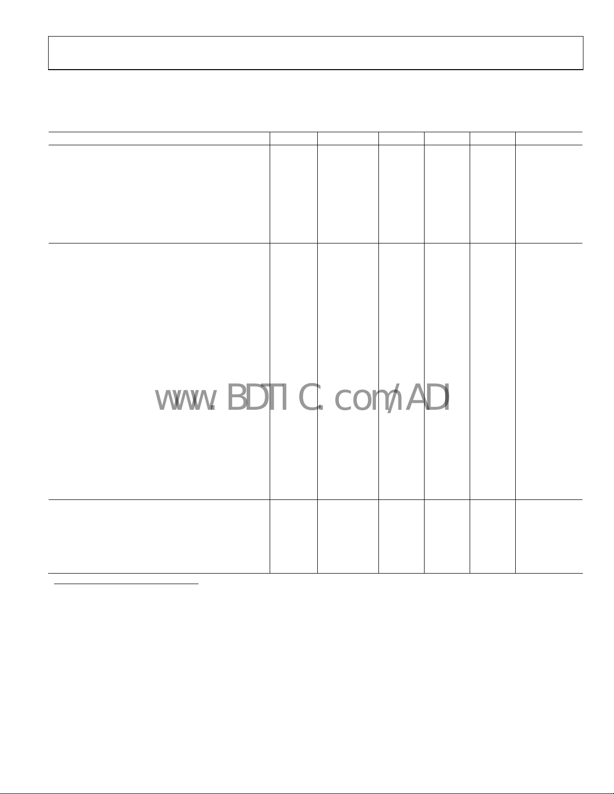
SPECIFICATIONS
VS = +3 V ± 5%, R
Table 1.
Parameter Temp Test Level Min Typ Max Unit
REF CLOCK INPUT CHARACTERISTICS
Frequency Range
REFCLK Multiplier Disabled Full VI 5 200
REFCLK Multiplier Enabled at 4 × Full VI 5 50 MHz
REFCLK Multiplier Enabled at 20 × Full VI 5 10 MHz
Duty Cycle 25°C V 50 %
Input Capacitance 25°C V 3 pF
Input Impedance 25°C V 100 MΩ
DAC OUTPUT CHARACTERISTICS
Resolution 12 Bits
Full-Scale Output Current 5 10 20 mA
Gain Error 25°C I −10 +10 %FS
Output Offset 25°C I 10 µ A
Differential Nonlinearity 25°C V 0.5 LSB
Integral Nonlinearity 25°C V 1 LSB
Output Capacitance 25°C V 5 pF
Phase Noise @ 1 kHz Offset, 40 MHz A
REFCLK Multiplier Enabled at 20× 25°C V −85 dBc/Hz
REFCLK Multiplier at 4× 25°C V −100 dBc/Hz
REFCLK Multiplier Disabled 25°C V −110 dBc/Hz
Voltage Compliance Range 25°C I −0.5 1.5 V
Wideband SFDR:
1 MHz Analog Out 25°C IV 70 dBc
20 MHz Analog Out 25°C IV 65 dBc
42 MHz Analog Out 25°C IV 60 dBc
65 MHz Analog Out 25°C IV 55 dBc
80 MHz Analog Out 25°C IV 50 dBc
Narrow-Band SFDR: (± 100 kHz Window)
70 MHz Analog Out 25°C IV 80 dBc
MODULATOR CHARACTERISTICS
Adjacent Channel Power (CH Power = −6.98 dBm) 25°C IV 50 dBm
Error Vector Magnitude 25°C IV 1 2 %
I/Q Offset 25°C IV 50 55 dB
Inband Spurious Emissions 25°C IV 45 50 dBc
Pass-Band Amplitude Ripple (DC to 80 MHz) 25°C V ±0.3 dB
1
For 200 MHz operation in modulation mode at 85°C operating temperature, VS must be 3 V minimum.
= 3.9 kΩ, external reference clock frequency = 10 MHz with REFCLK multiplier enabled at 20×.
SET
OUT
1
MHz
Rev. C | Page 3 of 36
AD9856
www.BDTIC.com/ADI
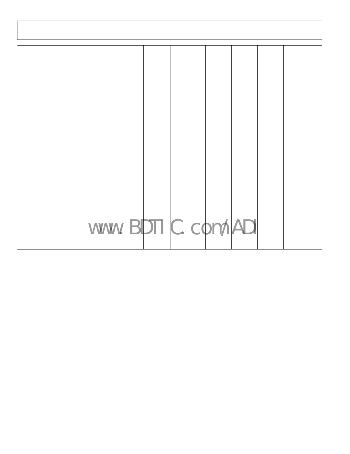
Parameter Temp Test Level Min Typ Max Unit
TIMING CHARACTERISTICS
Serial Control Bus
Maximum Frequency Full IV 10 MHz
Minimum Clock Pulse Width High (t
Minimum Clock Pulse Width Low (t
Maximum Clock Rise/Fall Time Full IV 1 ms
Minimum Data Setup Time (tDS) Full IV 25 ns
Minimum Data Hold Time (tDH) Full IV 0 ns
Maximum Data Valid Time (tDV) Full IV 30 ns
Wake-Up Time
Minimum RESET Pulse Width High (tRH) Full IV 5 REFCLK cycles
CMOS LOGIC INPUTS
Logic 1 Voltage 25°C I 2.6 V
Logic 0 Voltage 25°C I 0.4 V
Logic 1 Current 25°C I 12 µA
Logic 0 Current 25°C I 12 µA
Input Capacitance 25°C V 3 pF
CMOS LOGIC OUTPUTS (1 mA LOAD)
Logic 1 Voltage 25°C I 2.7 mA
Logic 0 Voltage 25°C I 0.4 mA
POWER SUPPLY
+VS Current
Full Operating Conditions
Burst Operation (25%) 25°C I 450 mA
Single-Tone Mode 25°C I 495 mA
160 MHz Clock 25°C I 445 mA
120 MHz Clock 25°C I 345 mA
Power-Down Mode 25°C I 2 mA
2
3
2
Assuming 1.3 kΩ and 0.01 µF loop filter components.
3
Assuming 1.3 kW and 0.01 mF loop filter components.
) Full IV 30 ns
PWH
) Full IV 30 ns
PWL
Full IV 1 ms
25°C I 530 mA
Rev. C | Page 4 of 36
AD9856
www.BDTIC.com/ADI
ABSOLUTE MAXIMUM RATINGS
Absolute maximum ratings are limiting values, to be applied
individually, and beyond which the serviceability of the circuit
may be impaired. Functional operability under any of these
conditions is not necessarily implied. Exposure of absolute
maximum rating conditions for extended periods of time may
affect device reliability.
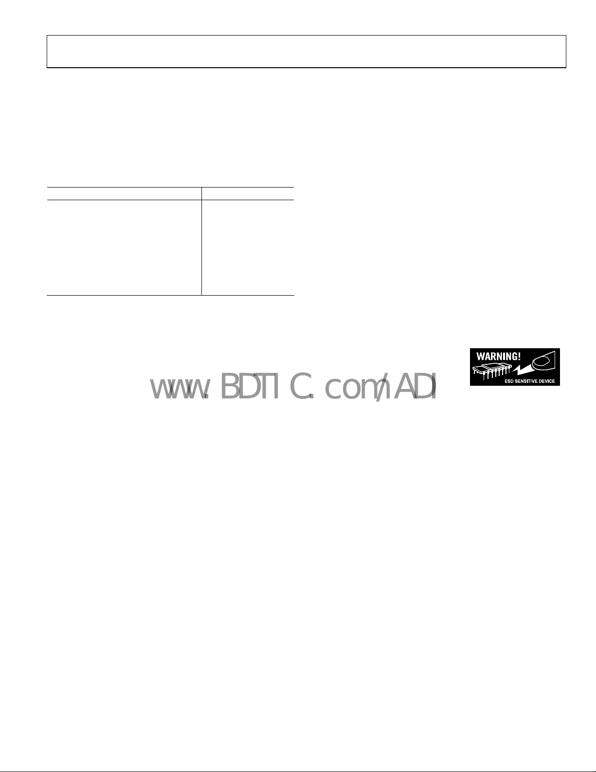
Table 2.
Parameter Rating
Maximum Junction Temperature 150°C
Storage Temperature −65°C to +150°C
V
S
Operating Temperature −40°C to +85°C
Digital Inputs −0.7 V to +V
Lead Temperature (Soldering 10 sec) 300°C
Digital Output Current 5 mA
θJA Thermal Impedance 38°C/W
4 V
s
ESD CAUTION
ESD (electrostatic discharge) sensitive device. Electrostatic charges as high as 4000 V readily accumulate on
the human body and test equipment and can discharge without detection. Although this product features
proprietary ESD protection circuitry, permanent damage may occur on devices subjected to high energy
electrostatic discharges. Therefore, proper ESD precautions are recommended to avoid performance
degradation or loss of functionality.
EXPLANATION OF TEST LEVELS
I. 100% production tested.
III. Sample tested only.
IV. Parameter is guaranteed by design and characterization
testing.
V. Parameter is a typical value only.
VI. Devices are 100% production tested at 25°C and
guaranteed by design and characterization testing for
industrial operating temperature range.
Rev. C | Page 5 of 36
AD9856
www.BDTIC.com/ADI
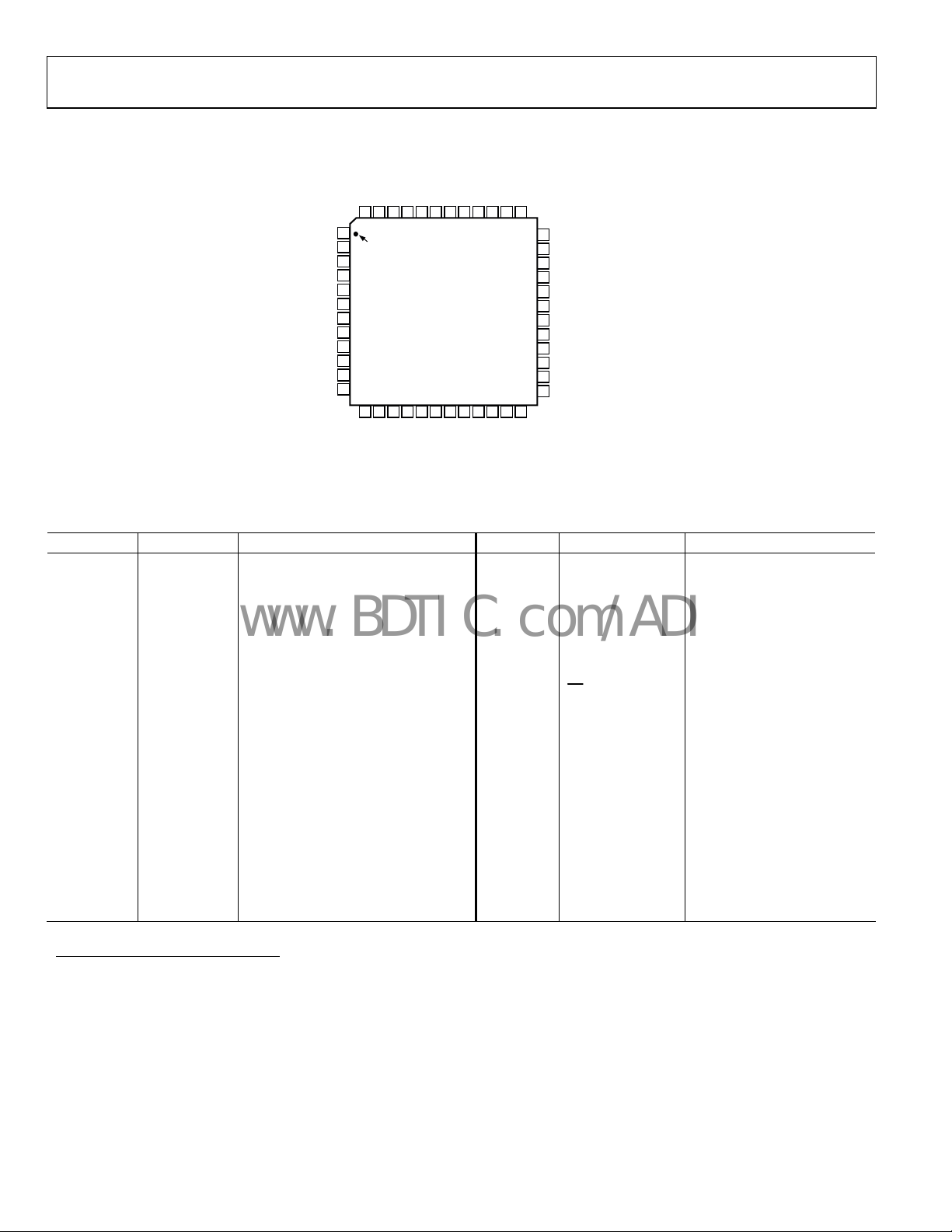
PIN CONFIGURATION AND FUNCTION DESCRIPTIONS
PS0
DVDD
DGND
AD9856
TOP VIEW
(Notto Scale)
D0
D1
NC
SYNC I/O
SDIO
SCLK
NC
DVDD
DGND
SDO
NC
CS
AGND
CA CLK
BG REF
BYPASS
36
CA DATA
35
CA ENABLE
34
PLL SUPPLY
33
PLL FILTER
32
PLL GND
31
AGND
30
I
OUT
29
I
OUTB
28
AGND
27
AVDD
26
DAC REF BYPASS
25
DAC R
SET
00637-C-002
D11
D10
DVDD
DGND
D9
D8
D7
D6
DVDD
DGND
D5
1
2
3
4
5
6
7
8
9
10
11
12
TxENABLE
NC =NO CONNECT
PS1
REFCLK
RESET
48 47 46 45 44 39 3843 42 41 40 37
PIN 1
IDENTIFIER
13 14 15 16 17 18 19 20 21 22 23 24
D3
D2
D4
Figure 2. Pin Configuration
Table 3. Pin Function Descriptions
Pin No. Mnemonic Pin Function Pin No. Mnemonic Pin Function
1 TxENABLE
Input Pulse that Synchronizes the
32 PLL GND PLL Ground
Data Stream
2 D11 Input Data (Most Significant Bit) 33 PLL FILTER PLL Loop Filter Connection
3 D10 Input Data 34 PLL SUPPLY PLL Voltage Supply
4, 10, 21, 44 DVDD Digital Supply Voltage 35 CA ENABLE Cable Driver Amp Enable
5, 11, 20, 43 DGND Digital Ground 36 CA DATA Cable Driver Amp Data
6 to 9 D9 to D6 Input Data 37 CA CLK Cable Driver Amp Clock
12 to 16 D5 to D1 Input Data 38
CS
Chip Select
17 D0 Input Data (Least Significant Bit) 39 SDO Serial Data Output
18, 19, 22 NC No Internal Connection 40 SDIO Serial Port I/O
23, 28, 31 AGND Analog Ground 41 SCLK Serial Port Clock
24
BG REF
No External Connection
1
42 SYNC I/O Performs I/O Synchronization
BYPASS
25 DAC R
26
DAC REF
R
SET
Resistor Connection 45 PS0 Profile Select 0
SET
1
No External Connection
46 PS1 Profile Select 1
BYPASS
27 AVDD Analog Supply Voltage 47 REFCLK Reference Clock Input
29 I
OUTB
Complementary Analog Current
48 RESET Master Reset
Output of the DAC
30 I
True Analog Current Output of DAC
OUT
1
In most cases, optimal performance is achieved with no external connection. For extremely noisy environments, BG REF BYPASS can be bypassed with up to a 0.1 µF
capacitor to AGND (Pin 23). DAC REF BYPASS can be bypassed with up to a 0.1 µF capacitor to AVDD (Pin 27).
Rev. C | Page 6 of 36
AD9856
www.BDTIC.com/ADI
Table 4. Functional Block Mode Descriptions
Functional Block Mode Description
Operating Modes 1. Complex quadrature modulator mode.
2. Single-tone output mode.
Input Data Format
Input Sample Rate Up to 50 Msamples/sec @ 200 MHz SYSCLK rate.
Input Reference
Clock Frequency
Internal Reference
Clock Multiplier
Profile Select Four pin-selectable, preprogrammed formats. Available for modulation and single-tone operating modes.
Interpolating Range Fixed 4×, selectable 2×, and selectable 2× to 63× range.
Half-Band Filters Interpolating filters that provide upsampling and reduce the effects of the CIC passband roll-off characteristics.
TxENABLE Function–
Burst Mode
TxENABLE Function–
Continuous Mode
Inverse SINC Filter Precompensates for SIN(x)/x roll-off of DAC; user bypassable.
I/Q Channel Invert
Full Sleep Mode Power dissipation reduced to less than 6 mW when full sleep mode is active; programmable via the control bus.
Programmable: 12-bit, 6-bit, or 3-bit input formats. Data inp
I/Q symbol component data is required to be at least 2× oversampled, depending upon configuration.
For DC to 80 MHz A
programmable via control bus; with REFCLK multiplier disabled: 200 MHz.
Note: For optimum data synchronization, the AD9856 reference clock and the input data clock should be derived
from the same clock source.
Programmable in integer steps over the range of 4× to 20×. Can be disabled (effective REFCLK multiplier = 1) via
control bus. Output of REFCLK multiplier = SYSCLK rate, which is the internal clock rate applied to the DDS and DAC
function.
When burst mode is enabled via the control bus, the rising edge of the applied TxENABLE pulse should be
coincident with, and frame, the input data packet. This establishes data sampling synchronization.
When continuous mode is enabled via the control bus, the TxENABLE pin becomes an I/Q control line. A Logic 1
on TxENABLE indicates I data is being presented to the AD9856. A Logic 0 on TxENABLE indicates Q data is being
presented to the AD9856. Each rising edge of TxENABLE resynchronizes the AD9856 input sampling capability.
[I ×Cos(ωt) + Q ×Sin(ωt)] or [I ×Cos(ωt) − Q ×Sin(ωt)] (default), configurable via control bus, per profile.
operation (200 MHz SYSCLK rate) with REFCLK multiplier enabled: 10 MHz to50 MHz,
OUT
ut to the AD9856 is 12-bit, twos complement. Complex
Rev. C | Page 7 of 36
AD9856
www.BDTIC.com/ADI
TYPICAL PERFORMANCE CHARACTERISTICS
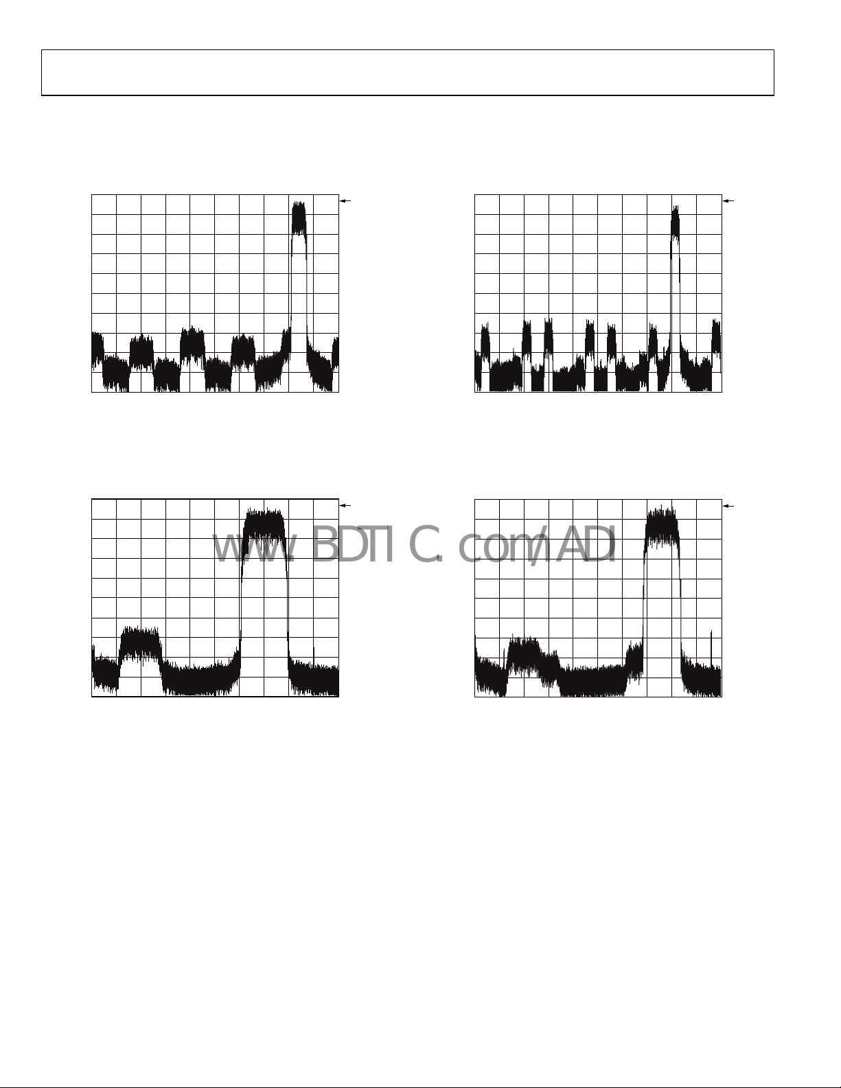
TYPICAL MODULATED OUTPUT SPECTRAL PLOTS
10dB
RF ATT
10kHz
REF LVL
–25dBm
0
–8
–16
–24
–32
–40
(dBm)
–48
–56
–64
–72
–80
Figure 3. QPSK at 42 MHz and 2.56 MS/sec; 10.24 MHz External Clock with
REFCLK Multiplier = 12, CIC = 3, HB3 On, 2× Data
REF LVL
–30dBm
0
–8
–16
–24
–32
–40
(dBm)
–48
–56
–64
–72
–80
0
Figure 4. 64-QAM at 28 MHz and 6 MS/sec; 36 MHz External Clock with
REFCLK Multiplier = 4, CIC = 2, HB3 Off, 3× Data
RBW
VBW
SWT
RBW
VBW
SWT
1kHz
12.5s
10kHz
1kHz
10s
UNIT
STOP 50MHzSTART 0Hz 5MHz/
RF ATT
UNIT
STOP 40MHzSTART 0Hz 4MHz/
dBm
10dB
dBm
1AP
1AP
00637-C-003
00637-C-004
VBW
SWT
20s
UNIT
dBm
1AP
STOP 80MHzSTART 0Hz 8MHz/
–16
–24
–32
–40
(dBm)
–48
–56
–64
–72
–80
0
–8
REF LVL
–25dBm
10dB
RF ATT
10kHz
RBW
1kHz
Figure 5. 16-QAM at 65 MHz and 2.56 MS/sec; 10.24 MHz External Clock with
REFCLK Multiplier = 18, CIC = 9, HB3 Off, 2× Data
VBW
SWT
12.5s
UNIT
dBm
1AP
STOP 50MHzSTART 0Hz 5MHz/
–16
–24
–32
–40
(dBm)
–48
–56
–64
–72
–80
0
–8
REF LVL
–30dBm
10dB
RF ATT
10kHz
RBW
1kHz
Figure 6. 256-QAM at 38 MHz and 6 MS/sec; 48 MHz External Clock with
REFCLK Multiplier = 4, CIC = 2, HB3 Off, 4× Data
00637-C-005
00637-C-006
Rev. C | Page 8 of 36
AD9856
www.BDTIC.com/ADI
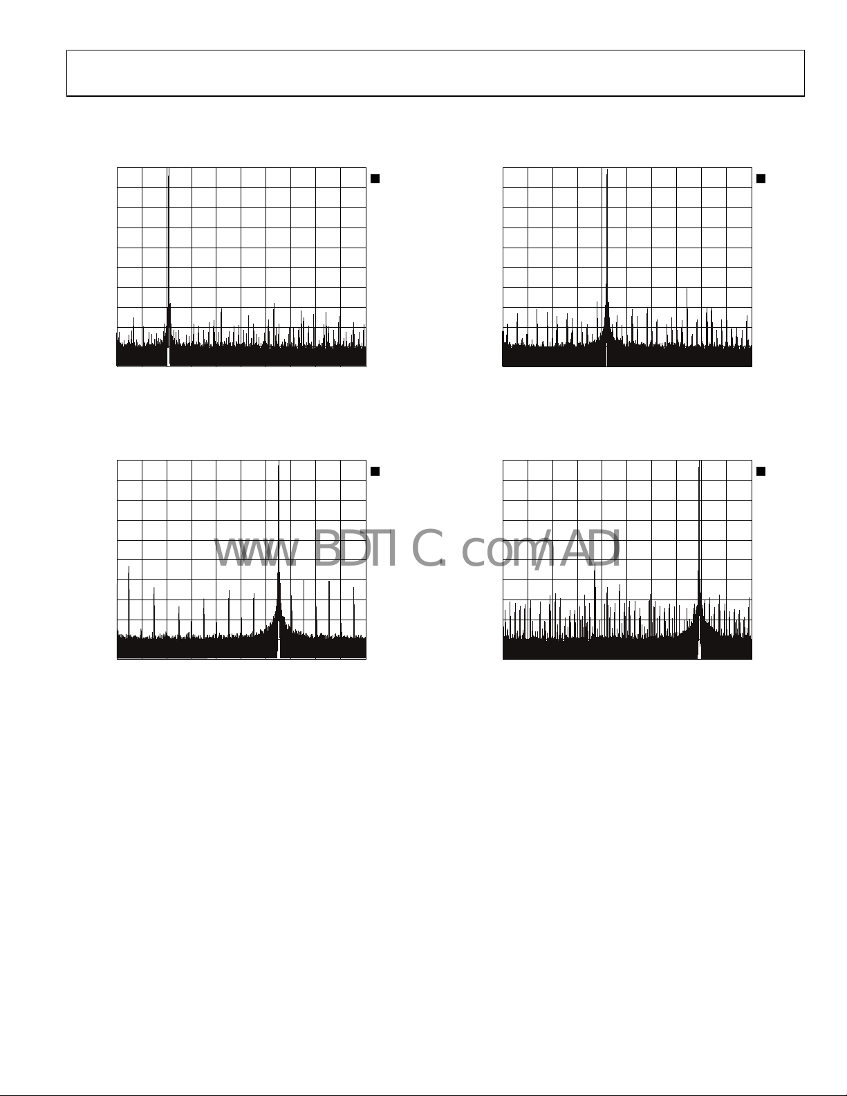
TYPICAL SINGLE-TONE OUTPUT SPECTRAL PLOTS
–10
–20
–30
–40
–50
(dBm)
–60
–70
–80
–90
–100
–10
–20
–30
–40
–50
(dBm)
–60
–70
–80
–90
–100
REF LVL
–5dBm
0
REF LVL
–5dBm
0
3kHz
RBW
3kHz
VBW
28s
SWT
Figure 7. 21 MHz CW Output
3kHz
RBW
3kHz
VBW
28s
SWT
Figure 8. 65 MHz CW Output
RF ATT
UNIT
STOP 100MHzSTART 0Hz 10MHz/
RF ATT
UNIT
STOP 100MHzSTART 0Hz 10MHz/
20dB
dB
20dB
dB
A
1AP
A
1AP
00637-C-007
00637-C-008
–10
–20
–30
–40
–50
(dBm)
–60
–70
–80
–90
–100
–10
–20
–30
–40
–50
(dBm)
–60
–70
–80
–90
–100
REF LVL
–5dBm
0
REF LVL
–5dBm
0
3kHz
RBW
3kHz
VBW
28s
SWT
Figure 9. 42 MHz CW Output
3kHz
RBW
3kHz
VBW
28s
SWT
Figure 10. 79 MHz CW Output
RF ATT
UNIT
STOP 100MHzSTART 0Hz 10MHz/
RF ATT
UNIT
STOP 100MHzSTART 0Hz 10MHz/
20dB
dB
A
1AP
00637-C-009
20dB
dB
A
1AP
00637-C-010
Rev. C | Page 9 of 36
AD9856
www.BDTIC.com/ADI
TYPICAL NARROW-BAND SFDR SPECTRAL PLOTS
20dB
RF ATT
100Hz
RBW
100Hz
REF LVL
–5dBm
0
–10
–20
–30
–40
–50
(dBm)
–60
–70
–80
–90
–100
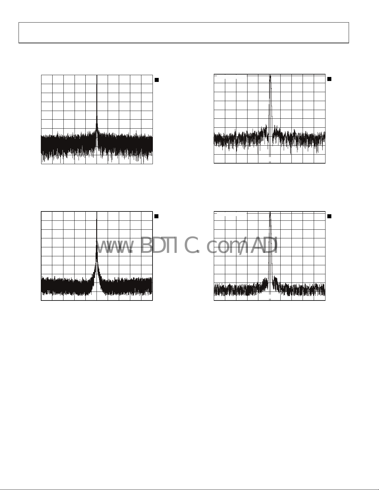
Figure 11. 70.1 MHz Narrow-Band SFDR, 10 MHz External Clock
with REFCLK Multiplier = 20×
REF LVL
–5dBm
0
–12
–24
–36
–48
–60
(dBm)
–72
–84
–96
–108
–120
Figure 12. 70.1 MHz Narrow-Band SFDR, 200 MHz External Clock
with REFCLK Multiplier Disabled
VBW
50s
SWT
100Hz
RBW
100Hz
VBW
50s dB
SWT
UNIT
SPAN 100kHzCENTER 70.1MHz 10kHz/
UNIT
SPAN 100kHzCENTER 70.1MHz 10kHz/
dB
A
1AP
20dBRF ATT
A
1AP
00637-C-011
00637-C-012
TYPICAL PHASE NOISE SPECTRAL PLOTS
RF ATT
30Hz
RBW
30Hz
VBW
28s
SWT
FXD
30Hz
RBW
30Hz
VBW
28s dB
SWT
FXD
UNIT
SPAN 5kHzCENTER 40.1MHz 500Hz/
UNIT
SPAN 5kHzCENTER 40.1MHz 500Hz/
–12
–24
–36
–48
–60
(dBm)
–72
–84
–96
–108
–120
–12
–24
–36
–48
–60
(dBm)
–72
–84
–96
–108
–120
REF LVL
0dBm
0
FXD –2.248dBm
Figure 13. 40.1 MHz Output, 10 MHz External Clock
with REFCLK Multiplier = 20×
REF LVL
0dBm
0
FXD –2.248dBm
Figure 14. 40.1 MHz Output, 200 MHz External Clock
with REFCLK Multiplier Disabled
30dB
dB
30dBRF ATT
A
1AP
A
1AP
00637-C-013
00637-C-014
Rev. C | Page 10 of 36
AD9856
www.BDTIC.com/ADI
TYPICAL PLOTS OF OUTPUT CONSTELLATIONS
TRACE A: CH 1 QPSK MEAS TIME
1.5
TRACE A: CH 1 256QAM MEAS TIME
1
CONST
300
M
/DIV
–1.5
–1.9607843757 1.96078437567
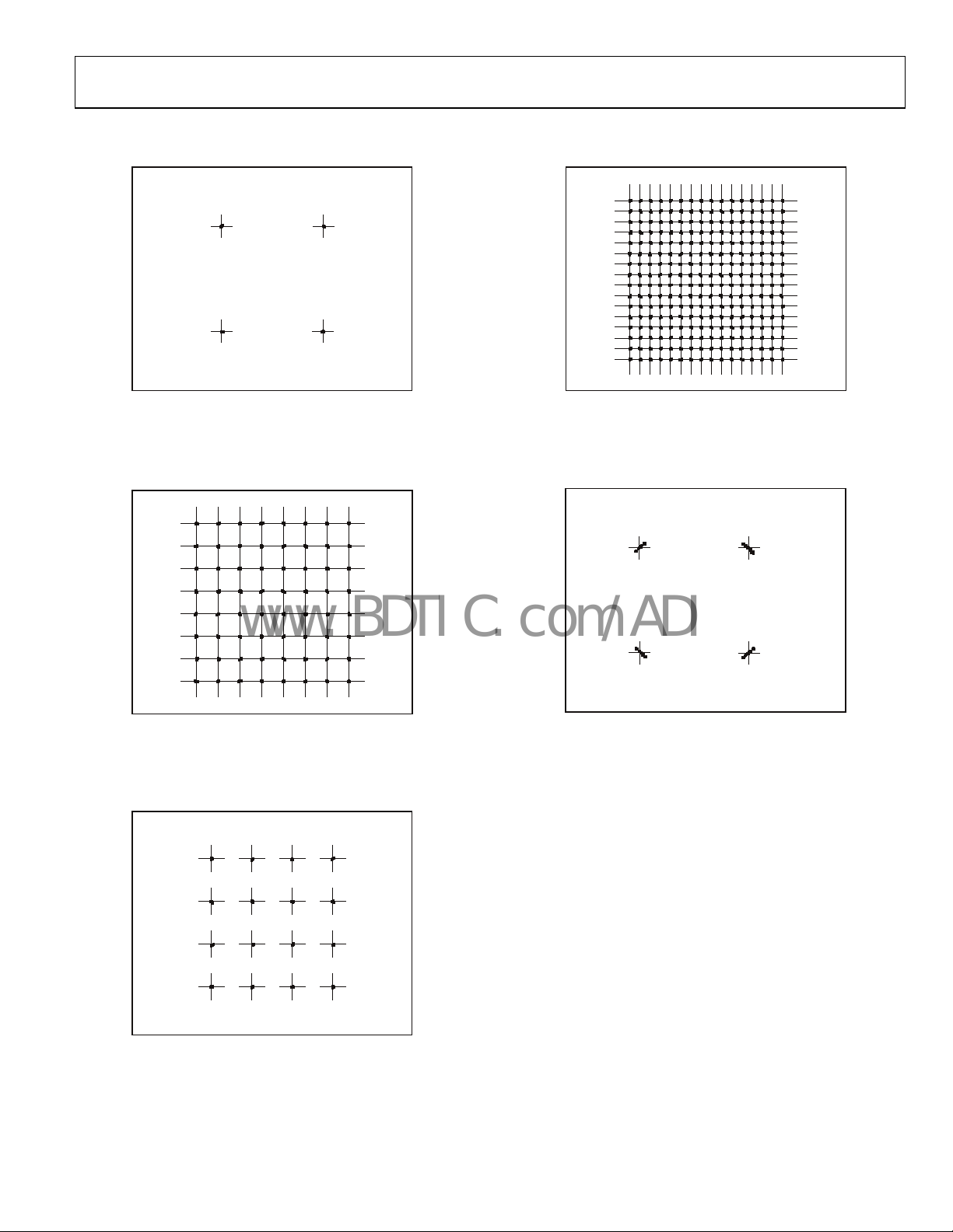
Figure 15. QPSK, 65 MHz, 2.56 MS/sec
TRACE A: CH 1 64QAM MEAS TIME
1
CONST
200
M
/DIV
00637-C-015
CONST
200
M
/DIV
–1
–1.3071895838 1.30718958378
Figure 18. 256-QAM, 42 MHz, 6 MS/sec
TRACE A: CH 1 MSK1 MEAS TIME
1.5
CONST
300
M
/DIV
00637-C-018
–1
–1.3071895838 1.30718958378
Figure 16. 64-QAM, 42 MHz, 6 MS/sec
TRACE A: CH 1 16QAM MEAS TIME
1.25
CONST
250
M
/DIV
–1.25
–1.6339869797 1.63398697972
Figure 17. 16-QAM, 65 MHz, 2.56 MS/sec
00637-C-016
00637-C-017
–1.5
–1.9607843757 1.96078437567
Figure 19. GMSK Modulation, 13 MS/sec
00637-C-019
Rev. C | Page 11 of 36
 Loading...