CMOS 300 MSPS Quadrature
L
FEATURES
300 MHz internal clock rate
FSK, BPSK, PSK, CHIRP, AM operation
Dual integrated 12-bit D/A converters
Ultrahigh speed comparator, 3 ps rms jitter
Excellent dynamic performance:
80 dB SFDR @ 100 MHz (±1 MHz) A
4× to 20× programmable reference clock multiplier
Dual 48-bit programmable frequency registers
Dual 14-bit programmable phase offset registers
12-bit amplitude modulation and programmable
shaped on/off keying function
Single-pin FSK and BPSK data interface
PSK capability via I/O interface
Linear or nonlinear FM chirp functions with single-pin
frequency hold function
Frequency-ramped FSK
< 25 ps rms total jitter in clock generator mode
REFERENCE
CLOCK IN
DIFF/SINGLE
SELECT
FSK/BPSK/HOLD
DATA IN
BIDIRECTIONAL
INTERNAL/EXTERNA
I/O UPDATE CLOCK
REF
CLK
BUFFER
SYSTEM
CLOCK
DEMUX
2
MODE SELECT
SYSTEM
CLOCK
3
FREQUENCY
48 48 48 14
DELTA
FREQUENCY
WORD
CK
D
INT
EXT
4× – 20×
REF CLK
MULTIPLIER
MUX
DELTA
RATE TIMER
SYSTEM
CLOCK
FREQUENCY
Q
OUT
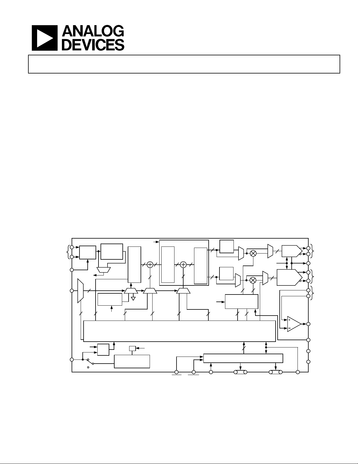
FUNCTIONAL BLOCK DIAGRAM
SYSTEM CLOCK
ACC 1
FREQUENCY
ACCUMULATOR
MUX
TUNING
WORD 1
PROGRAMMABLE
UPDATE CLOCK
FREQUENCY
÷2
INTERNAL
48
MUX MUX
TUNING
WORD 2
SYSTEM
CLOCK
Automatic bidirectional frequency sweeping
SIN(x)/x correction
Simplified control interfaces:
3.3 V single supply
Multiple power-down functions
Single-ended or differential input reference clock
Small 80-lead LQFP packaging
APPLICATIONS
Agile, quadrature LO frequency synthesis
Programmable clock generators
FM chirp source for radar and scanning systems
Test and measurement equipment
Commercial and amateur RF exciters
DDS CORE
4848
PHASE
ACCUMULATOR
FIRST 14-BIT
PHASE/OFFSET
PROGRAMMING REGISTERS
17
17
ACC 2
14
SECOND 14-BIT
WORD
PHASE/OFFSET
AD9854
READ WRITE SERIAL/
Figure 1.
Complete DDS
AD9854
10 MHz serial, 2-wire or 3-wire SPI®-compatible
100 MHz parallel 8-bit programming
DIGITAL MULTIPLIERS
INV.
12
I
PHASE-TO-
12
AMPLITUDE
CONVERTER
Q
SYSTEM
CLOCK
14
WORD
PARALLEL
SELECT
SINC
FILTER
FILTER
MUX
INV.
SINC
MUX
12
PROGRAMMABLE
AMPLITUDE AND
RATE CONTROL
12
12
"I" AND "Q" 12-BIT
AM MODULATION
I/O PORT BUFFERS
6-BIT ADDRESS
OR SERIAL
PROGRAMMING
LINES
BUS
SYSTEM
CLOCK
MUX
12
12-BIT DC
CONTROL
MUX
12
12
"Q" DAC OR
CONTROL
8-BIT
PARALLEL
LOAD
12-BIT
"I"
DAC
12-BIT
DAC
COMPARATOR
MASTER
RESET
ANALOG
OUT
DAC R
ANALOG
OUT
ANALOG
IN
CLOCK
OUT
SHAPED
ON/OFF
KEYING
GND
+V
S
SET
00636-B-001
Rev. C
Information furnished by Analog Devices is believed to be accurate and reliable.
However, no responsibility is assumed by Analog Devices for its use, nor for any
infringements of patents or other rights of third parties that may result from its use.
Specifications subject to change without notice. No license is granted by implication
or otherwise under any patent or patent rights of Analog Devices. Trademarks and
registered trademarks are the property of their respective owners.
One Technology Way, P.O. Box 9106, Norwood, MA 02062-9106, U.S.A.
Tel: 781.329.4700
Fax: 781.326.8703 © 2004 Analog Devices, Inc. All rights reserved.
www.analog.com

AD9854
TABLE OF CONTENTS
General Description ..........................................................................3
Specifications......................................................................................4
Absolute Maximum Ratings.............................................................8
Explanation of Test Levels........................................................... 8
Pin Configuration and Function Descriptions..............................9
Typical Performance Characteristics ........................................... 12
Typical Applications ....................................................................... 16
Theory of Operation ...................................................................... 19
Modes of Operation ................................................................... 19
Using the AD9854 .......................................................................... 28
General Operation of the Serial Interface....................................35
Instruction Byte .......................................................................... 36
Serial Interface Port Pin Descriptions..................................... 36
Notes on Serial Port Operation ................................................ 36
MSB/LSB Transfers..........................................................................37
Control Register Description.................................................... 37
Power Dissipation and Thermal Considerations........................39
Thermal Impedance................................................................... 39
Junction Temperature Considerations .................................... 39
Internal and External Update Clock........................................ 28
Shaped On/Off Keying .............................................................. 28
I and Q DACs.............................................................................. 29
Control DAC............................................................................... 29
Inverse SINC Function .............................................................. 30
REFCLK Multiplier.................................................................... 30
Programming the AD9854............................................................ 32
Parallel I/O Operation ............................................................... 33
Serial Port I/O Operation.......................................................... 33
REVISION HISTORY
9/04—Data Sheet Changed from Rev. B to Rev. C
Updated Format..................................................................Universal
Changes to Table 1............................................................................ 4
Changes to Footnote 2 ..................................................................... 7
Changes to Explanation of Test Levels Section ............................ 8
Changes to Theory of Operation Section.................................... 17
Changes to Single Tone (Mode 000) Section .............................. 17
Changes to Ramped FSK (Mode 010) Section ........................... 18
Changes to Basic FM Chirp Programming Steps Section......... 23
Changes to Figure 50...................................................................... 27
Changes to Evaluation Board Operating Instructions Section 40
Changes to Filtered IOUT1 and the Filtered IOUT2 Section... 41
Changes to Using the Provided Software Section ...................... 42
Changes to Figure 68...................................................................... 45
Changes to Figure 69...................................................................... 46
Updated Outline Dimensions....................................................... 50
Changes to Ordering Guide.......................................................... 50
Evaluation of Operating Conditions........................................ 40
Thermally Enhanced Package Mounting Guidelines............ 41
Evaluation Board .............................................................................42
Evaluation Board Instructions.................................................. 42
General Operating Instructions ............................................... 42
Using the Provide d Sof tware .................................................... 44
Support ........................................................................................ 44
Outline Dimensions ........................................................................51
Ordering Guide .......................................................................... 51
3/02—Data Sheet Changed from Rev. A to Rev. B
Updated Format.................................................................. Universal
Renumbered Figures and Tables ......................................Universal
Changes to General Description Section .......................................1
Changes to Functional Block Diagram...........................................1
Changes to Specifications Section...................................................4
Changes to Absolute Maximum Ratings Section..........................7
Changes to Pin Function Descriptions...........................................8
Changes to Figure 3........................................................................ 10
Deleted two Typical Performance Characteristics Graphs....... 11
Changes to Inverse SINC Function Section................................ 28
Changes to Differential REFCLK Enable Section...................... 28
Changes to Figure 52...................................................................... 30
Changes to Parallel I/O Operation Section................................. 32
Changes to General Operation of the Serial Interface Section 33
Changes to Figure 57...................................................................... 34
Replaced Operating Instructions Section ................................... 40
Changes to Figure 68...................................................................... 44
Changes to Figure 69...................................................................... 45
Changes to Customer Evaluation Board Table........................... 46
Rev. C | Page 2 of 52

AD9854
GENERAL DESCRIPTION
The AD9854 digital synthesizer is a highly integrated device
that uses advanced DDS technology, coupled with two internal
high speed, high performance quadrature D/A converters to
form a digitally programmable I and Q synthesizer function.
When referenced to an accurate clock source, the AD9854
generates highly stable, frequency-phase amplitude-programmable sine and cosine outputs that can be used as an agile LO
in communications, radar, and many other applications. The
AD9854’s innovative high speed DDS core provides 48-bit
frequency resolution (1 MHz tuning resolution with 300 MHz
SYSCLK). Maintaining 17 bits assures excellent SFDR. The
AD9854’s circuit architecture allows the generation of
taneous quadrature output signals at frequencies up to
150 MHz, which can be digitally tuned at a rate of up to
100 million new frequencies per second. The sine wave output
(externally filtered) can be converted to a square wave by the
internal comparator for agile clock generator applications.
The device provides two 14-bit phase registers and a single pin
for BPSK operation. For higher-order PSK operation, the I/O
interface may be used for phase changes. The 12-bit I and
Q DACs, coupled with the innovative DDS architecture, provide
excellent wideband and narrow-band output SFDR. The Q DAC
can also be configured as a user-programmable control DAC if
simul-
the quadrature function is not desired. When configured with
the comparator, the 12-bit control DAC facilitates static duty
cycle control in high speed clock generator applications. Two
12-bit digital multipliers permit programmable amplitude
modulation, shaped on/off keying, and precise amplitude
control of the quadrature output. Chirp functionality is also
included to facilitate wide bandwidth frequency sweeping
applications. The AD9854’s programmable 4× to 20× REFCLK
multiplier circuit generates the 300 MHz system clock internally
from a lower frequency external reference clock. This saves the
user the expense and difficulty of implementing a 300 MHz
system clock source. Direct 300 MHz clocking is also accommodated with either single-ended or differential inputs. Singlepin conventional FSK and the enhanced spectral qualities of
ramped FSK are supported.The AD9854 uses advanced 0.35
micron CMOS technology to provide a high level of
functionality on a single 3.3 V supply.
The AD9854 is available in a space-saving 80-lead LQFP
surface-mount package and a thermally enhanced 80-lead
LQFP package. The AD9854 is pin-for-pin compatible with the
AD9852 single-tone synthesizer. It is specified to operate over
the extended industrial temperature range of −40°C to +85°C.
Rev. C | Page 3 of 52

AD9854
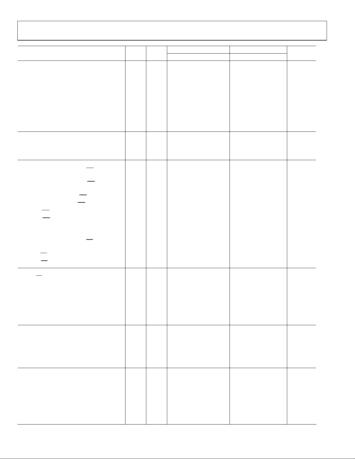
SPECIFICATIONS
VS = 3.3 V ± 5%, R
external reference clock frequency = 20 MHz with REFCLK multiplier enabled at 10× for AD9854AST, unless otherwise noted.
Table 1.
AD9854ASQ AD9854AST
Parameter Temp
REF CLOCK INPUT CHARACTERISTICS
Internal System Clock Frequency Range
REFCLK Multiplier Enabled Full VI 20 300 20 200 MHz
REFCLK Multiplier Disabled Full VI DC 300 DC 200 MHz
External REF Clock Frequency Range
REFCLK Multiplier Enabled Full VI 5 75 5 50 MHz
REFCLK Multiplier Disabled Full VI DC 300 DC 200 MHz
Duty Cycle 25°C IV 45 50 55 45 50 55 %
Input Capacitance 25°C IV 3 3 pF
Input Impedance 25°C IV 100 100 kΩ
Differential Mode Common-Mode
Voltage Range
Minimum Signal Amplitude
Common-Mode Range 25°C IV 1.6 1.75 1.9 1.6 1.75 1.9 V
VIH (Single-Ended Mode) 25°C IV 2.3 2.3 V
VIL (Single-Ended Mode) 25°C IV 1 1 V
DAC STATIC OUTPUT CHARACTERISTICS
Output Update Speed Full I 300 200 MSPS
Resolution 25°C IV 12 12 Bits
I and Q Full-Scale Output Current 25°C IV 5 10 20 5 10 20 mA
I and Q DAC DC Gain Imbalance
Gain Error 25°C I −6 +2.25 −6 +2.25 % FS
Output Offset 25°C I 2 2 µA
Differential Nonlinearity 25°C I 0.3 1.25 0.3 1.25 LSB
Integral Nonlinearity 25°C I 0.6 1.66 0.6 1.66 LSB
Output Impedance 25°C IV 100 100 kΩ
Voltage Compliance Range 25°C I −0.5 +1.0 −0.5 +1.0 V
DAC DYNAMIC OUTPUT CHARACTERISTICS
I and Q DAC Quad. Phase Error 25°C IV 0.2 1 0.2 1 Degrees
DAC Wideband SFDR
1 MHz to 20 MHz A
20 MHz to 40 MHz A
40 MHz to 60 MHz A
60 MHz to 80 MHz A
80 MHz to 100 MHz A
100 MHz to 120 MHz A
DAC Narrow-Band SFDR
10 MHz A
10 MHz A
10 MHz A
41 MHz A
41 MHz A
41 MHz A
119 MHz A
119 MHz A
119 MHz A
= 3.9 kΩ, external reference clock frequency = 30 MHz with REFCLK multiplier enabled at 10× for AD9854ASQ,
SET
Te st
Level
1
Min Typ Max Min Typ Max Unit
2
3
OUT
OUT
OUT
OUT
OUT
OUT
(±1 MHz) 25°C V 83 83 dBc
OUT
(±250 kHz) 25°C V 83 83 dBc
OUT
(±50 kHz) 25°C V 91 91 dBc
OUT
(±1 MHz) 25°C V 82 82 dBc
OUT
(±250 kHz) 25°C V 84 84 dBc
OUT
(±50 kHz) 25°C V 89 89 dBc
OUT
(±1 MHz) 25°C V 71 71 dBc
OUT
(±250 kHz) 25°C V 77 77 dBc
OUT
(±50 kHz) 25°C V 83 83 dBc
OUT
25°C IV 400 400 mV p-p
25°C I −0.5 +0.15 +0.5 −0.5 +0.15 +0.5 dB
25°C V 58 58 dBc
25°C V 56 56 dBc
25°C V 52 52 dBc
25°C V 48 48 dBc
25°C V 48 48 dBc
25°C V 48 48 dBc
Rev. C | Page 4 of 52

AD9854
AD9854ASQ AD9854AST
Parameter Temp
Residual Phase Noise
(A
= 5 MHz, Ext. CLK = 30 MHz,
OUT
REFCLK Multiplier Engaged at 10×)
1 kHz Offset 25°C V 140 140 dBc/Hz
10 kHz Offset 25°C V 138 138 dBc/Hz
100 kHz Offset 25°C V 142 142 dBc/Hz
(A
= 5 MHz, Ext. CLK = 300 MHz,
OUT
REFCLK Multiplier Bypassed)
1 kHz Offset 25°C V 142 142 dBc/Hz
10 kHz Offset 25°C V 148 148 dBc/Hz
100 kHz Offset 25°C V 152 152 dBc/Hz
Pipeline Delays
DDS Core (Phase Accumulator and
4, , 5 6
25°C IV 33 33
Phase-to-Amp Converter)
Frequency Accumulator 25°C IV 26 26
Inverse Sinc Filter 25°C IV 16 16
Digital Multiplier 25°C IV 9 9
DAC 25°C IV 1 1
I/O Update Clock (INT MODE) 25°C IV 2 2
I/O Update Clock (EXT MODE) 25°C IV 3 3
MASTER RESET DURATION 25°C IV 10 10
COMPARATOR INPUT CHARACTERISTICS
Input Capacitance 25°C V 3 3 pF
Input Resistance 25°C IV 500 500 kΩ
Input Current 25°C I ±1 ±5 ±1 ±5 µA
Hysteresis 25°C IV 10 20 10 20 mV p-p
COMPARATOR OUTPUT CHARACTERISTICS
Logic 1 Voltage, High Z Load Full VI 3.1 3.1 V
Logic 0 Voltage, High Z Load Full VI 0.16 0.16 V
Output Power, 50 Ω Load,
25°C I 9 11 9 11 dBm
120 MHz Toggle Rate
Propagation Delay 25°C IV 3 3 ns
Output Duty Cycle Error
7
25°C I −10 ±1 +10 −10 ±1 +10 %
Rise/Fall Time, 5 pF Load 25°C V 2 2 ns
Toggle Rate, High Z Load 25°C IV 300 350 300 350 MHz
Toggle Rate, 50 Ω Load 25°C IV 375 400 375 400 MHz
Output Cycle-to-Cycle Jitter
8
IV 4.0 4.0 Ps rms
Te st
Level
Min Typ Max Min Typ Max Unit
SysClk
Cycles
SysClk
Cycles
SysClk
Cycles
SysClk
Cycles
SysClk
Cycles
SysClk
Cycles
SysClk
Cycles
SysClk
Cycles
Rev. C | Page 5 of 52
AD9854
AD9854ASQ AD9854AST
Parameter Temp
COMPARATOR NARROW-BAND SFDR
9
10 MHz (±1 MHz) 25°C V 84 84 dBc
10 MHz (±250 MHz) 25°C V 84 84 dBc
10 MHz (±50 MHz) 25°C V 92 92 dBc
41 MHz (±1 MHz) 25°C V 76 76 dBc
41 MHz (±250 MHz) 25°C V 82 82 dBc
41 MHz (±50 MHz) 25°C V 89 89 dBc
119 MHz (±1 MHz) 25°C V 73 dBc
119 MHz (±250 MHz) 25°C V 73 dBc
119 MHz (±50 MHz) 25°C V 83 dBc
CLOCK GENERATOR OUTPUT JITTER9
5 MHz A
OUT
40 MHz A
100 MHz A
OUT
OUT
25°C V 23 23 Ps rms
25°C V 12 12 Ps rms
25°C V 7 7 Ps rms
PARALLEL I/O TIMING CHARACTERISTICS
T
(Address Setup Time to WR Signal
ASU
Full IV 8.0 7.5 8.0 7.5 ns
Active)
T
(Address Hold Time to WR Signal
ADHW
Full IV 0 0 ns
Inactive)
T
(Data Setup Time to WR Signal Inactive)
DSU
T
(Data Hold Time to WR Signal Inactive)
DHD
T
(WR Signal Minimum Low Time)
WRLOW
T
(WR Signal Minimum High Time)
WRHIGH
Full IV 3.0 1.6 3.0 1.6 ns
Full IV 0 0 ns
Full IV 2.5 1.8 2.5 1.8 ns
Full IV 7 7 ns
TWR (Minimum Write Time) Full IV 10.5 10.5 ns
T
(Address to Data Valid Time) Full V 15 15 15 15 ns
ADV
T
(Address Hold Time to RD Signal
ADHR
Full IV 5 5 ns
Inactive)
T
(RD Low-to-Output Valid)
RDLOV
T
(RD High-to-Data Three-State)
RDHOZ
Full IV 15 15 ns
Full IV 10 10 ns
SERIAL I/O TIMING CHARACTERISTICS
T
(CS Setup Time)
PRE
T
(Period of Serial Data Clock) Full IV 100 100 ns
SCLK
T
(Serial Data Setup Time) Full IV 30 30 ns
DSU
T
(Serial Data Clock Pulse Width High) Full IV 40 40 ns
SCLKPWH
T
(Serial Data Clock Pulse Width Low) Full IV 40 40 ns
SCLKPWL
T
(Serial Data Hold Time) Full IV 0 0 ns
DHLD
Full IV 30 30 ns
TDV (Data Valid Time) Full V 30 30 ns
CMOS LOGIC INPUTS
10
Logic 1 Voltage 25°C I 2.2 2.2 V
Logic 0 Voltage 25°C I 0.8 0.8 V
Logic 1 Current 25°C IV ±5 ±12 µA
Logic 0 Current 25°C IV ±5 ±12 µA
Input Capacitance 25°C V 3 3 pF
POWER SUPPLY
+VS Current
+VS Current
+VS Current
12
P
25°C I 3.475 4.190 2.490 3.000 W
DISS
13
P
25°C I 2.345 2.825 1.700 2.025 W
DISS
14
P
25°C I 1.975 2.375 1.435 1.715 W
DISS
P
Power-Down Mode 25°C I 1 50 1 50 mW
DISS
11
12
13
14
25°C I 1050 1210 755 865 mA
25°C I 710 816 515 585 mA
25°C I 600 685 435 495 mA
Te st
Level
Min Typ Max Min Typ Max Unit
Rev. C | Page 6 of 52

AD9854
1
The reference clock inputs are configured to accept a 1 V p-p (typical) dc offset square or sine wave centered at one-half the applied VDD or a 3 V TTL-level pulse input.
2
An internal 400 mV p-p differential voltage swing equates to 200 mV p-p applied to both REFCLK input pins.
3
The I and Q gain imbalance is digitally adjustable to less than 0.01 dB.
4
Pipeline delays of each individual block are fixed; however, if the eight top MSBs of a tuning word are all zeros, the delay appears longer. This is due to insufficient
phase accumulation per a system CLK period to produce enough LSB amplitude to the D/A converter.
5
If a feature such as the inverse sinc, which has 16 pipeline delays, can be bypassed, the total delay is reduced by that amount.
6
The I/O update CLK transfers data from the I/O port buffers to the programming registers. This transfer is measured in system clocks.
7
Change in duty cycle from 1 MHz to 100 MHz with 1 V p-p sine wave input and 0.5 V threshold.
8
Represents comparator’s inherent cycle-to-cycle jitter contribution. Input signal is a 1 V, 40 MHz square wave. Measurement device Wavecrest DTS – 2075.
9
Comparator input originates from analog output section via external 7-pole elliptic LPF. Single-ended input, 0.5 V p-p. Comparator output terminated in 50 Ω.
10
Avoid overdriving digital inputs. (Refer to equivalent circuits in .) Figure 3
11
Simultaneous operation at the maximum ambient temperature of 85°C and the maximum internal clock frequency of 200 MHz for the 80-lead LQFP, or 300 MHz for
the thermally enhanced 80-lead LQFP, may cause the maximum die junction temperature of 150°C to be exceeded. Refer to the
Considerations
12
All functions engaged.
13
All functions except inverse sinc engaged.
14
All functions except inverse sinc and digital multipliers engaged.
section for derating and thermal management information.
Power Dissipation and Thermal
Rev. C | Page 7 of 52
AD9854
ABSOLUTE MAXIMUM RATINGS
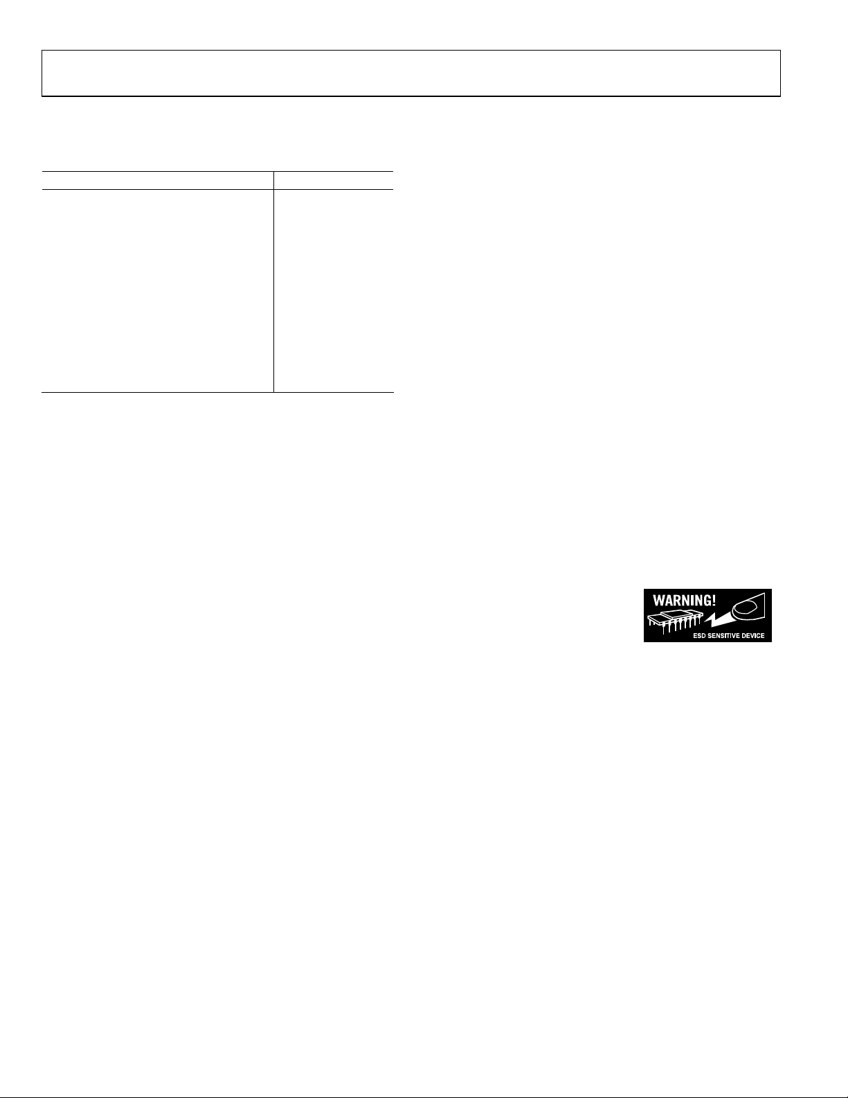
Table 2.
Parameter Rating
Maximum Junction Temperature 150°C
V
S
Digital Inputs −0.7 V to +V
Digital Output Current 5 mA
Storage Temperature −65°C to +150°C
Operating Temperature −40°C to +85°C
Lead Temperature (Soldering, 10 s) 300°C
Maximum Clock Frequency (ASQ) 300 MHz
Maximum Clock Frequency (AST) 200 MHz
θJA (ASQ) 16°C/W
θJA (AST) 38°C/W
θJC (ASQ) 2°C/W
4 V
S
Stresses above those listed under Absolute Maximum Ratings
may cause permanent damage to the device. This is a stress
rating only; functional operation of the device at these or any
other conditions above those indicated in the operational
section of this specification is not implied. Exposure to absolute
maximum rating conditions for extended periods may affect
device reliability.
EXPLANATION OF TEST LEVELS
1. 100% production tested.
3. Sample tested only.
4. Parameter is guaranteed by design and characterization
testing.
5. Parameter is a typical value only.
6. Devices are 100% production tested at 25°C and
guaranteed by design and characterization testing for
industrial operating temperature range.
ESD CAUTION
ESD (electrostatic discharge) sensitive device. Electrostatic charges as high as 4000 V readily accumulate on
the human body and test equipment and can discharge without detection. Although this product features
proprietary ESD protection circuitry, permanent damage may occur on devices subjected to high energy
electrostatic discharges. Therefore, proper ESD precautions are recommended to avoid performance
degradation or loss of functionality.
Rev. C | Page 8 of 52
AD9854
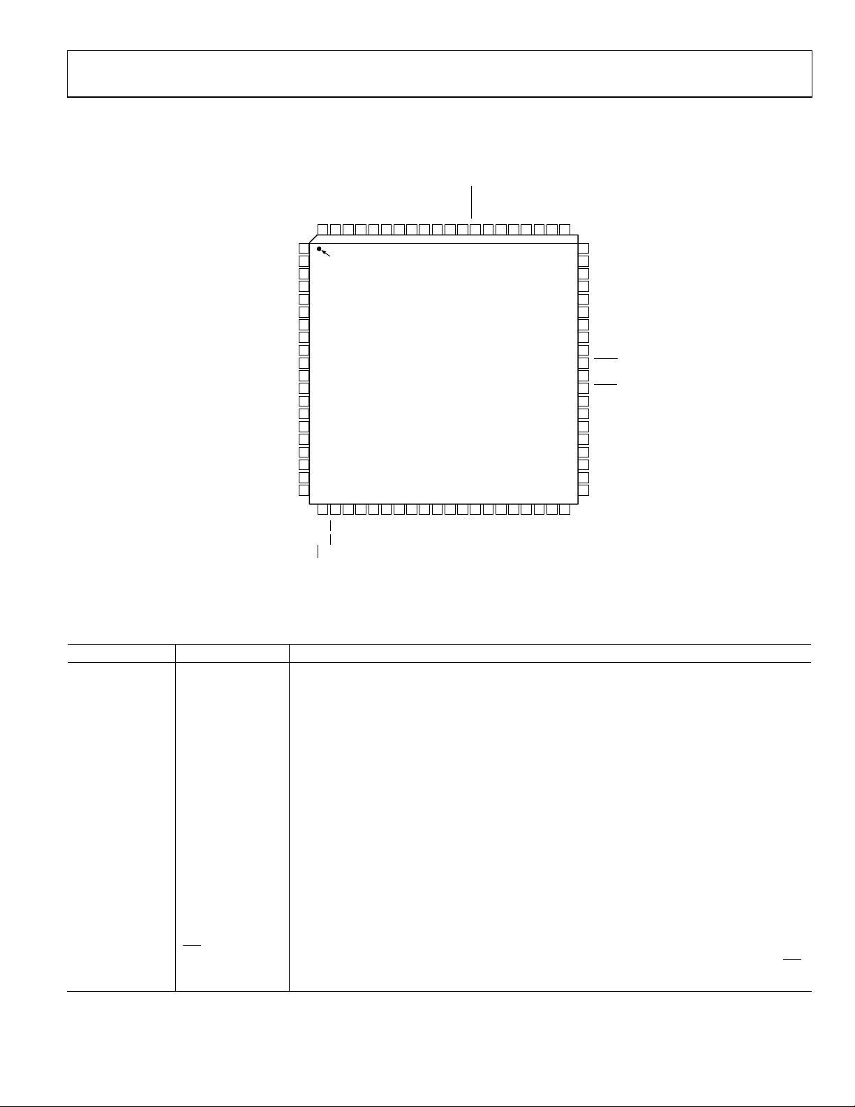
PIN CONFIGURATION AND FUNCTION DESCRIPTIONS
DVDD
DVDD
DGND
DGND
DGND
DGND
DVDD
DVDD
DGND
MASTER RESET
S/P SELECT
REFCLK
REFCLK
AGND
AGND
AVDD
DIFF CLK ENABLENCAGND
AVDD
AVDD
PLL FILTER
AGND
AGND
60
59
58
57
56
55
54
53
52
51
50
49
48
47
46
45
44
43
42
41
AVDD
AGND
NC
NC
DAC R
DACBP
AVDD
AGND
IOUT2
IOUT2
AVDD
IOUT1
IOUT1
AGND
AGND
AGND
AVDD
VINN
VINP
AGND
SET
D7
D6
D5
D4
D3
D2
D1
D0
DVDD
DVDD
DGND
DGND
NC
A5
A4
A3
A2/IO RESET
A1/SDO
A0/SDIO
I/O UD CLK
80 79 78 77 76 71 70 69 6875 74 73 72
1
PIN 1
2
INDICATOR
3
4
5
6
7
8
9
10
11
12
13
14
15
16
17
18
19
20
21 22 23 24 25 26 27 28 29 30 31 32 33
DVDD
DVDD
DVDD
RD/CS
WR/SCLK
DGND
DGND
AD9854
TOP VIEW
(Not to Scale)
DGND
34 35 36 37 38 39 40
AVDD
AVDD
AGND
AGND
NC
64 63 62 6167 66 65
VOUT
NC = NO CONNECT
SHAPED KEYING
00634-B-002
FSK/BPSK/HOLD
Figure 2. Pin Configuration
Table 3. Pin Function Descriptions
Pin No. Mnemonic Description
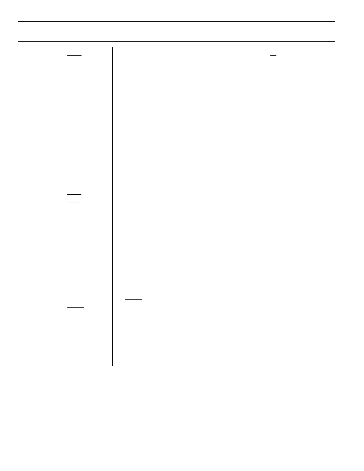
1 to 8 D7 to D0 8-Bit Bidirectional Parallel Programming Data Inputs. Used only in parallel programming mode.
9, 10, 23, 24, 25,
73, 74, 79, 80
11, 12, 26, 27, 28,
DVDD
Connections for the Digital Circuitry Supply Voltage. Nominally 3.3 V more positive than AGND
and DGND.
DGND Connections for Digital Circuitry Ground Return. Same potential as AGND.
72, 75, 76, 77, 78
13, 35, 57, 58, 63 NC No Internal Connection.
14 to 19 A5 toA0
Six-Bit Parallel Address Inputs for Program Registers. Used only in parallel programming mode.
Pin 17 (A2), Pin 18 (A1), and Pin 19 (A0) have a second function when the serial programming
mode is selected, as described next.
(17) A2/IO RESET
Allows an IO RESET of the serial communications bus that is unresponsive due to improper
programming protocol. Resetting the serial bus in this manner does not affect previous
programming nor does it invoke the default programming values listed in Table 7. Active high.
(18) A1/SDO Unidirectional Serial Data Output. Used in 3-wire serial communication mode.
(19) A0/SDIO Bidirectional Serial Data Input/Output. Used in 2-wire serial communication mode.
20 I/O UD CLK
Bidirectional I/O Update CLK. Direction is selected in control register. If selected as an input, a
rising edge transfers the contents of the I/O port buffers to the programming registers. If I/O UD
CLK is selected as an output (default), an output pulse (low to high) of an eight-system-clock-
cycle duration indicates that an internal frequency update has occurred.
21
WR/SCLK Write Parallel Data to I/O Port Buffers. Shared function with SCLK. Serial clock signal associated
with the serial programming bus. Data is registered on the rising edge. This pin is shared with
when the parallel mode is selected. Mode dependent on Pin 70 (S/P select).
WR
Rev. C | Page 9 of 52
AD9854
Pin No. Mnemonic Description
22
29 FSK/BPSK/HOLD
30 SHAPED KEYING
31, 32, 37, 38, 44,
50, 54, 60, 65
33, 34, 39, 40, 41,
45, 46, 47, 53, 59,
62, 66, 67
36 VOUT
42 VINP Voltage Input Positive. The internal high speed comparator’s noninverting input.
43 VINN Voltage Input Negative. The internal high speed comparator’s inverting input.
48 IOUT1 Unipolar Current Output of the I or Cosine DAC. (Refer to Figure 3.)
49
51
52 IOUT2
55 DACBP
56 DAC R
61 PLL FILTER
64 DIFF CLK ENABLE
68
69 REFCLK
70 S/P SELECT Selects Serial Programming Mode (Logic low) or Parallel Programming Mode (Logic High).
71 MASTER RESET
RD/CS Read Parallel Data from Programming Registers. Shared function with CS. Chip-select signal
associated with the serial programming bus. Active Low. This pin is shared with
RD when parallel
mode is selected.
Multifunction pin according to the mode of operation selected in the programming control
register. In FSK mode, logic low selects F1, logic high selects F2. In BPSK mode, logic low selects
Phase 1, logic high selects Phase 2. In chirp mode, logic high engages the hold function, causing
the frequency accumulator to halt at its current location. To resume or commence chirp mode,
logic low is asserted.
Must first be selected in the programming control register to function. A logic high causes the I
and Q DAC outputs to ramp up from zero-scale to full-scale amplitude at a preprogrammed rate.
Logic low causes the full-scale output to ramp down to zero scale at the preprogrammed rate.
AVDD
Connections for the Analog Circuitry Supply Voltage. Nominally 3.3 V more positive than AGND
and DGND.
AGND Connections for Analog Circuitry Ground Return. Same potential as DGND.
Internal High Speed Comparator’s Noninverted Output Pin. Designed to drive 10 dBm to 50 Ω
load as well as standard CMOS logic levels.
IOUT1
IOUT2
Complementary Unipolar Current Output of the I or Cosine DAC.
Complementary Unipolar Current Output of the Q or Sine DAC.
Unipolar Current Output of the Q or Sine DAC. This DAC can be programmed to accept external
12-bit data in lieu of internal sine data, allowing the AD9854 to emulate the AD9852 control DAC
function.
Common Bypass Capacitor Connection for both I and Q DACs. A 0.01 µF chip capacitor from this
pin to AVDD improves harmonic distortion and SFDR slightly. No connect is permissible (slight
SFDR degradation).
SET
Common Connection for both I and Q DACs to set the full-scale output current. R
Normal R
range is from 8 kΩ (5 mA) to 2 kΩ (20 mA).
SET
= 39.9/I
SET
Provides the connection for the external zero compensation network of the REFCLK multiplier’s
PLL loop filter. The zero compensation network consists of a 1.3 kΩ resistor in series with a 0.01 µF
capacitor. The other side of the network should be connected to AVDD as close as possible to
Pin 60. For optimum phase noise performance, the REFCLK multiplier can be bypassed by setting
the Bypass PLL bit in Control Register 1E.
Differential REFCLK Enable. A high level of this pin enables the differential clock inputs, REFCLK
REFCLK (Pins 69 and 68, respectively).
and
REFCLK The Complementary Differential Clock Signal (180 Degrees Out of Phase). User should tie this pin
high or low when single-ended clock mode is selected. Same signal levels as REFCLK.
Single-Ended Reference Clock Input (CMOS Logic Levels Required) or One of Two Differential
Clock Signals. In differential ref clock mode, both inputs can be CMOS logic levels or have greater
than 400 mV p-p square or sine waves centered about 1.6 V dc.
Initializes the serial/parallel programming bus to prepare for user programming; sets
programming registers to a do-nothing state defined by the default values listed in Table 7.
Active on logic high. Asserting master reset is essential for proper operation on power-up.
OUT
.
Rev. C | Page 10 of 52
AD9854
AVDD
I
OUTIOUTB
MUST TERMINATE OUTPUTS
FOR CURRENT FLOW. DO
NOT EXCEED THE OUTPUT
VOLTAGE COMPLIANCE RATING.
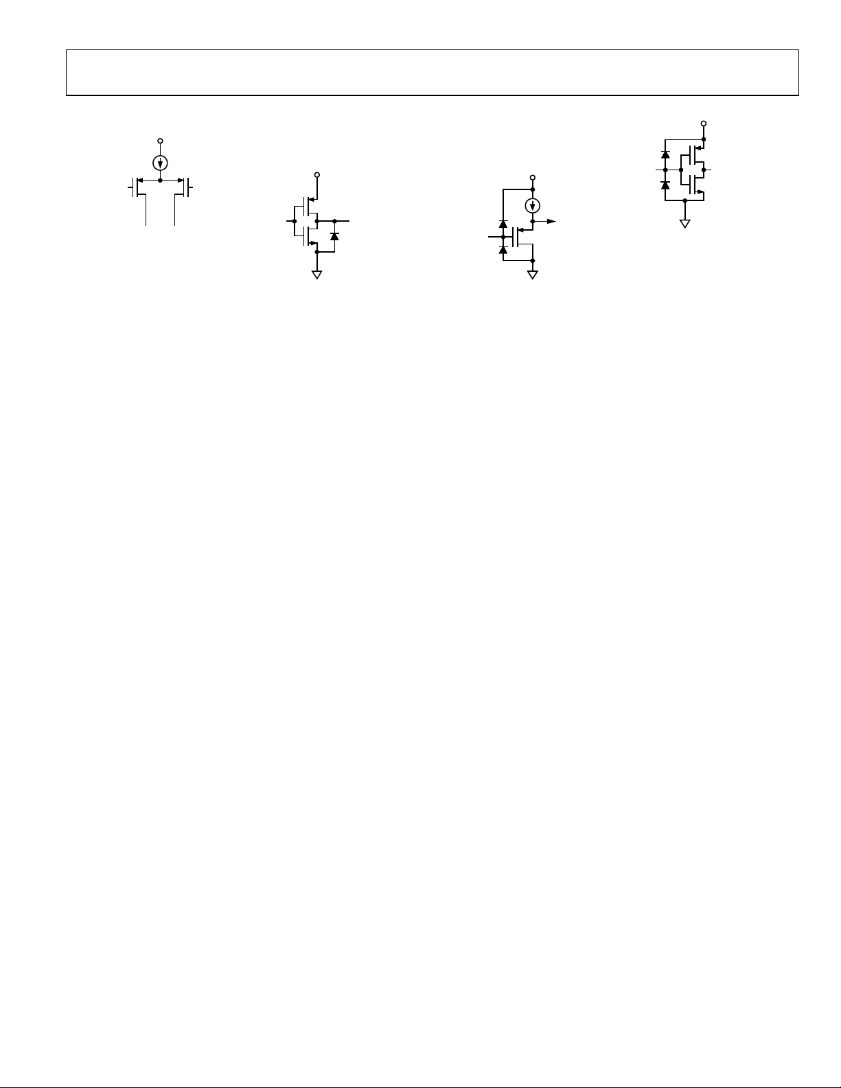
A. DAC OUTPUTS B. COMPARATOR OUTPUT C. COMPARATOR INPUT D. DIGITAL INPUTS
AVDD
VINP/
COMPARATOR
OUT
VINN
Figure 3. Equivalent Input and Output Circuits
AVDD
DVDD
DIGITAL
IN
AVOID OVERDRIVING
DIGITAL INPUTS. FORWARD
BIASING ESD DIODES MAY
COUPLE DIGITAL NOISE
ONTO POWER PINS.
00636-B-003
Rev. C | Page 11 of 52
AD9854
TYPICAL PERFORMANCE CHARACTERISTICS
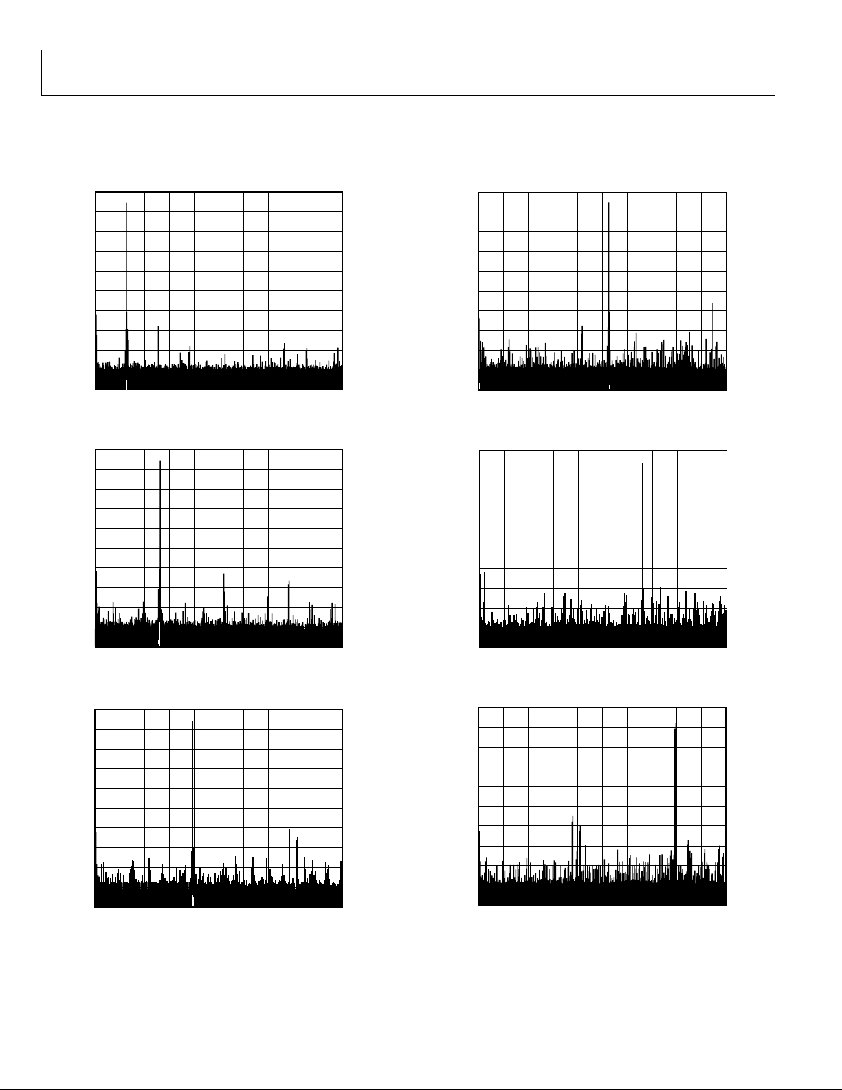
Figure 4 to Figure 9 indicate the wideband harmonic distortion performance of the AD9854 from 19.1 MHz to 119.1 MHz fundamental
output, reference clock = 30 MHz, REFCLK multiplier = 10. Each graph plotted from 0 MHz to 150 MHz (Nyquist).
0
–10
–20
–30
–40
–50
–60
–70
–80
–90
–100
0
–10
–20
–30
–40
–50
–60
–70
–80
–90
–100
0
–10
–20
–30
–40
–50
–60
–70
–80
–90
–100
START 0Hz
START 0Hz
START 0Hz
15MHz/ STOP 150MHz
Figure 4. Wideband SFDR, 19.1 MHz
15MHz/ STOP 150MHz
Figure 5. Wideband SFDR, 39.1 MHz
15MHz/ STOP 150MHz
Figure 6. Wideband SFDR, 59.1 MHz
00636-0-004
00636-0-005
00636-0-006
–10
–20
–30
–40
–50
–60
–70
–80
–90
–100
–10
–20
–30
–40
–50
–60
–70
–80
–90
–100
–10
–20
–30
–40
–50
–60
–70
–80
–90
–100
0
START 0Hz
0
START 0Hz
0
START 0Hz
15MHz/ STOP 150MHz
Figure 7. Wideband SFDR, 79.1 MHz
15MHz/ STOP 150MHz
Figure 8. Wideband SFDR, 99.1 MHz
15MHz/ STOP 150MHz
Figure 9. Wideband SFDR, 119.1 MHz
00636-0-007
00636-B-008
00636-B-009
Rev. C | Page 12 of 52
AD9854
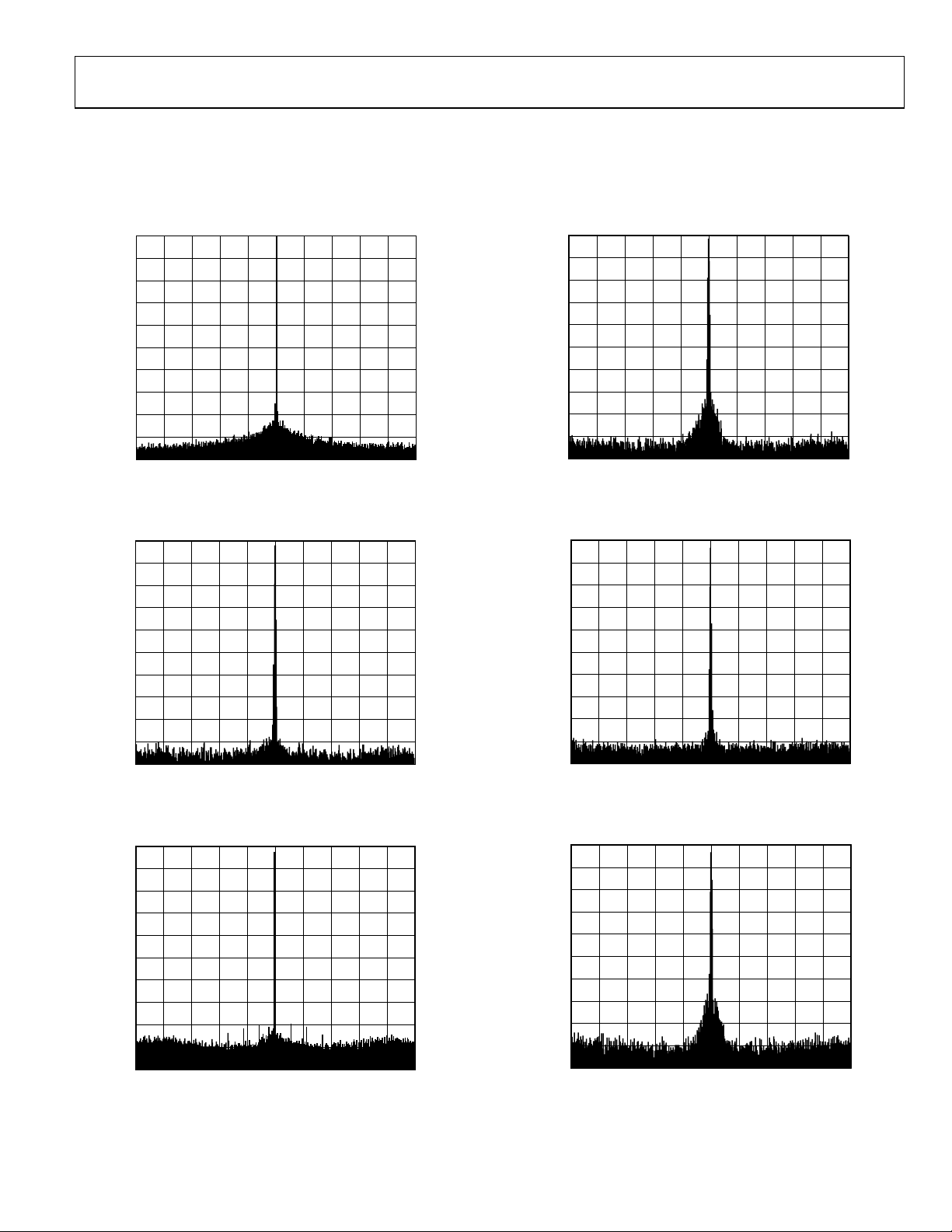
Figure 10 to Figure 13 show the trade-off in elevated noise floor, increased phase noise, and discrete spurious energy when the internal
REFCLK multiplier circuit is engaged. Plots with wide (1 MHz) and narrow (50 kHz) spans are shown. Compare the noise floor of
Figure 11 and Figure 13 to Figure 14 and Figure 15. The improvement seen in Figure 11 and Figure 13 is a direct result of sampling the
fundamental at a higher rate. Sampling at a higher rate spreads the quantization noise of the DAC over a wider bandwidth, which
effectively lowers the noise floor.
0
–10
–20
–30
–40
–50
–60
–70
–80
–90
–100
CENTER 39.1MHz
100kHz/ SPAN 1MHz
Figure 10. Narrow-Band SFDR, 39.1 MHz, 1 MHz BW,
300 MHz REFCLK with REFCLK Multiply Bypassed
0
–10
–20
–30
–40
–50
–60
–70
–80
–90
–100
CENTER 39.1MHz
5kHz/ SPAN 50kHz
Figure 11. Narrow-Band SFDR, 39.1 MHz, 50 kHz BW,
300 MHz REFCLK with REFCLK Multiply Bypassed
0
–10
–20
–30
–40
–50
–60
–70
–80
–90
–100
CENTER 39.1MHz
100kHz/ SPAN 1MHz
Figure 12. Narrow-Band SFDR, 39.1 MHz, 1 MHz BW,
30 MHz REFCLK with REFCLK Multiply = 10x
0
–10
–20
–30
–40
–50
–60
–70
–80
–90
–100
00636-B-010
CENTER 39.1MHz
5kHz/ SPAN 50kHz
00636-B-013
Figure 13. Narrow-Band SFDR, 39.1 MHz, 50 kHz BW,
30 MHz REFCLK with REFCLK Multiply = 10x
0
–10
–20
–30
–40
–50
–60
–70
–80
–90
–100
00636-B-011
CENTER 39.1MHz
5kHz/ SPAN 50kHz
00636-B-014
Figure 14. Narrow-Band SFDR, 39.1 MHz, 50 kHz BW,
100 MHz REFCLK with REFCLK Multiply Bypassed
0
–10
–20
–30
–40
–50
–60
–70
–80
–90
–100
00636-B-012
CENTER 39.1MHz
5kHz/ SPAN 50kHz
00636-B-015
Figure 15. Narrow-Band SFDR, 39.1 MHz, 50 kHz BW,
10 MHz REFCLK with REFCLK Multiply = 10x
Rev. C | Page 13 of 52
AD9854
–
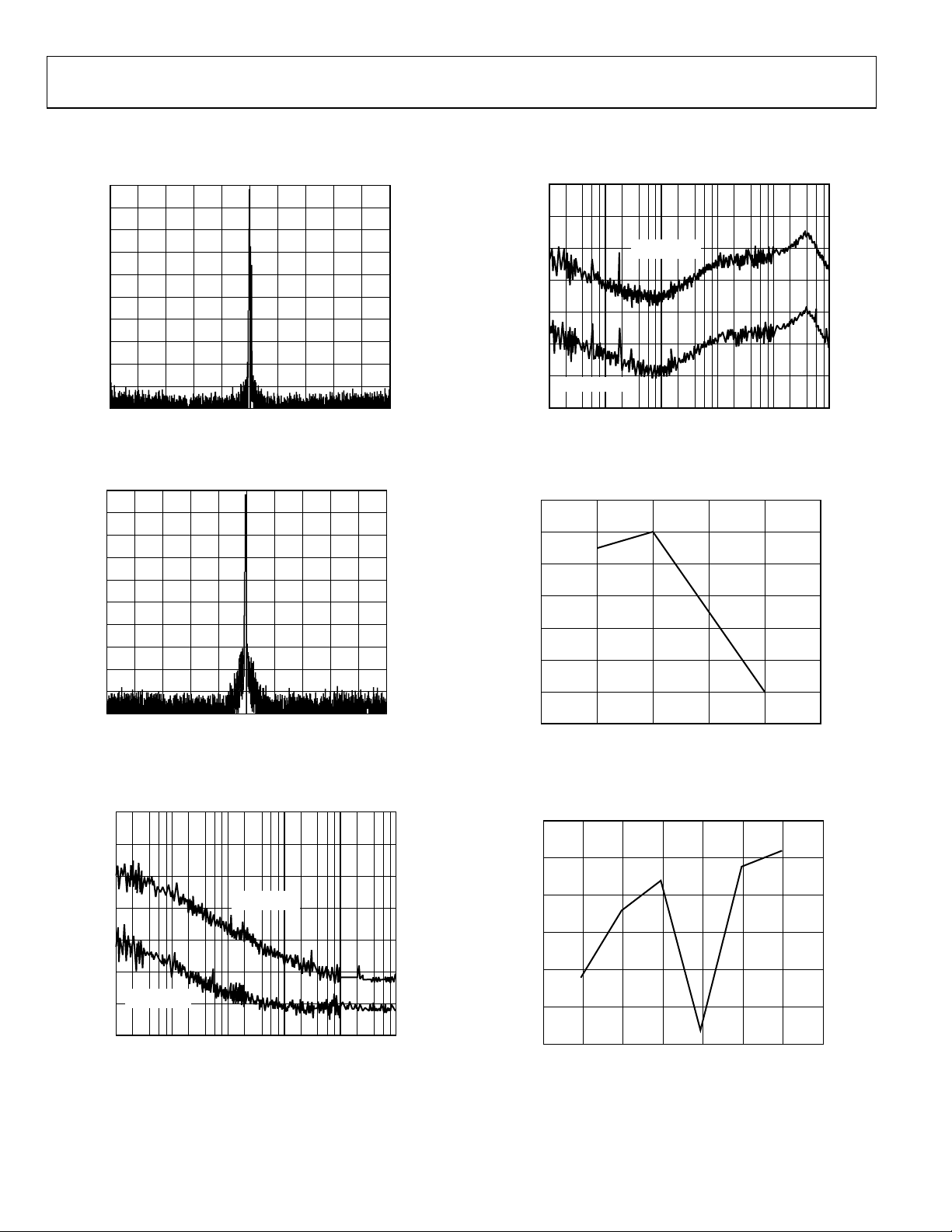
Figure 16 and Figure 17 show the narrow-band performance of the AD9854 when operating with a 20 MHz reference clock and the
REFCLK multiplier enabled at 10× vs. a 200 MHz reference clock with REFCLK multiplier bypassed.
0
–10
–20
–30
–40
–50
–60
–70
–80
–90
–100
CENTER 39.1MHz
5kHz/ SPAN 50kHz
Figure 16. Narrow-Band SFDR, 39.1 MHz, 50 kHz BW,
200 MHz REFCLK with REFCLK Multiply Bypassed
0
–10
–20
–30
–40
–50
–60
–70
–80
–90
100
CENTER 39.1MHz
5kHz/ SPAN 50kHz
Figure 17. Narrow-Band SFDR, 39.1 MHz, 50 kHz BW,
20 MHz REFCLK with REFCLK Multiply = 10x
–100
–110
–120
A
= 80MHz
–130
–140
OUT
–90
–100
A
–110
–120
–130
–140
PHASE NOISE (dBc/Hz)
–150
A
= 5MHz
OUT
00636-B-016
–160
10 1M100 100k10k1k
= 80MHz
OUT
FREQUENCY (Hz)
00636-B-019
Figure 19. Residual Phase Noise, 30 MHz REFCLK with
REFCLK Multiplier = 10x
55
54
53
52
51
SFDR (dBc)
50
49
00636-B-017
48
0
510152025
DAC CURRENT (mA)
Figure 20. SFDR vs. DAC Current, 59.1 A
, 300 MHz
OUT
00636-B-020
REFCLK with REFCLK Multiplier Bypassed
620
615
610
605
–150
PHASE NOISE (dBc/Hz)
A
= 5MHz
–160
–170
OUT
10 1M100 100k10k1k
FREQUENCY (Hz)
00636-B-018
600
SUPPLY CURRENT (mA)
595
590
0
20 40 60 80 100 120 140
FREQUENCY (MHz)
00636-B-021
Figure 18. Residual Phase Noise, 300 MHz REFCLK with
REFCLK Multiplier Bypassed
Figure 21. Supply Current vs. Output Frequency; Variation
Is Minimal as a Percentage and Heavily Dependent on Tuning Word
Rev. C | Page 14 of 52
AD9854
1200
MINIMUM COMPARATOR
INPUT DRIVE
= 0.5V
V
CM
1000
RISE TIME
1.04ns
[10.6ps RMS]
–33ps 0ps +33ps
Ω
500ps/DIV 232mV/DIV 50
INPUT
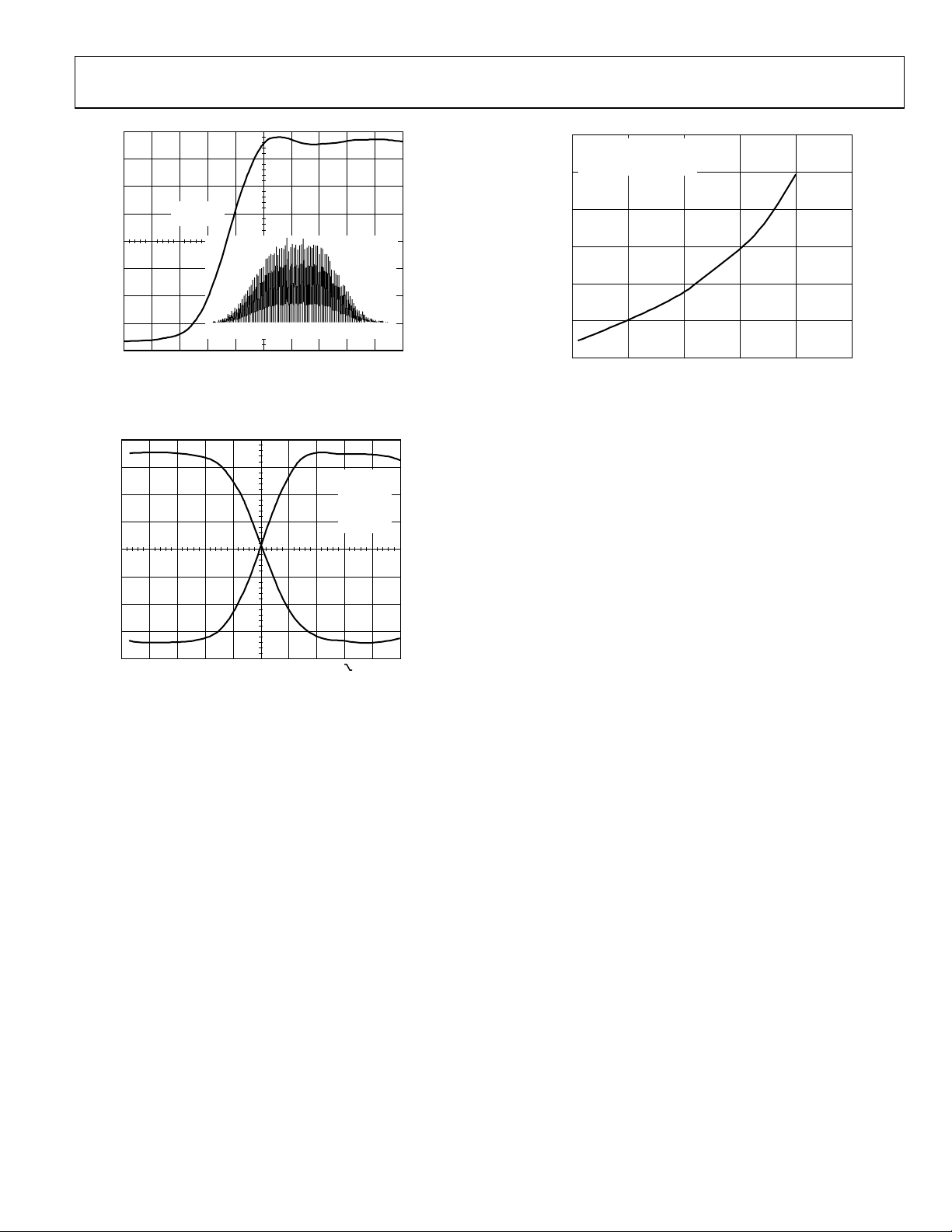
Figure 22. Typical Comparator Output Jitter, 40 MHz A
with REFCLK Multiplier Bypassed
REF1 RISE
1.174ns
C1 FALL
1.286ns
JITTER
, 300 MHz RFCLK
OUT
800
600
400
AMPLITUDE (mV p-p)
200
00636-B-022
0
0
100 200 300 400 500
FREQUENCY (MHz)
00636-B-024
Figure 24. Comparator Toggle Voltage Requirement
CH1 500mV
Ω
M 500ps CH1 980mV
Figure 23. Comparator Rise/Fall Times
00636-B-023
Rev. C | Page 15 of 52
AD9854
TYPICAL APPLICATIONS
RF IN
RF/IF
INPUT
REFCLK
AD9854
LPF
LPF
COS
SIN
LPF
CHANNEL
SELECT
FILTERS
LPF
I BASEBAND
Q BASEBAND
00636-B-025
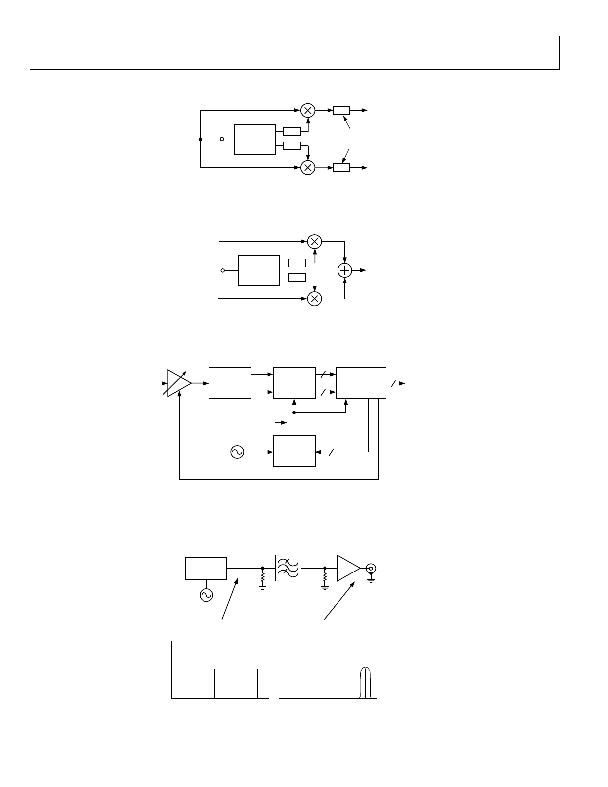
Figure 25. Quadrature Downconversion
I BASEBAND
COS
Q BASEBAND
REFCLK
AD9854
LPF
LPF
SIN
RF OUTPUT
00636-B-026
Figure 26. Direct Conversion Quadrature Upconver ter
Rx
VCA
I/Q MIXER
AND
LOW-PASS
FILTER
ADC CLOCK FREQUENCY
LOCKED TO Tx CHIP/
SYMBOL/PN RATE
I
DUAL
8-/10-BIT
Q
ADC
AD9854
CLOCK
REFERENCE
CLOCK
GENERATOR
8
8
ADC ENCODE
48
CHIP/SYMBOL/PN
RATE DATA
DIGITAL
DEMODULATOR
AGC
Rx BASEBAND
DIGITAL DATA
OUT
00636-B-027
Figure 27. Chip Rate Generator in Spread Spectrum Application
AD9854
I
OUT
50
Ω
BAND-PASS
FILTER
50
AMPLIFIER
Ω
AD9854
SPECTRUM
FUNDAMENTAL
F
C
IMAGE
– F
+ F
F
O
C
O
IMAGE
F
CLK
FINAL OUTPUT
SPECTRUM
Figure 28. Using an Aliased Image to Generate a High Frequency
Rev. C | Page 16 of 52
FC + F
IMAGE
O
BAND-PASS
FILTER
00636-B-028
 Loading...