REV. C
Information furnished by Analog Devices is believed to be accurate and
reliable. However, no responsibility is assumed by Analog Devices for its
use, nor for any infringements of patents or other rights of third parties
which may result from its use. No license is granted by implication or
otherwise under any patent or patent rights of Analog Devices.
a
AD9853
One Technology Way, P.O. Box 9106, Norwood, MA 02062-9106, U.S.A.
Tel: 781/329-4700 World Wide Web Site: http://www.analog.com
Fax: 781/326-8703 © Analog Devices, Inc., 1999
Programmable Digital
QPSK/16-QAM Modulator
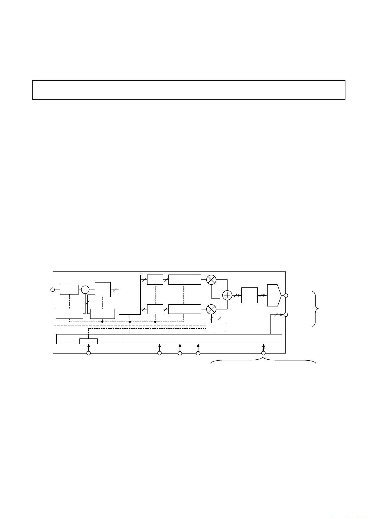
FUNCTIONAL BLOCK DIAGRAM
10-BIT
DAC
SINE COSINE
INTERPOLATION
FILTER
INV
SYNC
FILTER
DDS
PREAMBLE
INSERTION
RANDOMIZER
CLOCK
CONTROL FUNCTIONS
63
FIR
FILTER
FIR
FILTER
INTERPOLATION
FILTER
ENCODER:
FSK
QPSK
DQPSK
16-QAM
D16-QAM
DATA
DELAY
& MUX
XOR
R-S
FEC
AD9853
10 10
A
OUT
GAIN
CONTROL TO
DRIVER AMP
RESET
T
X
ENABLE
FEC
ENABLE/
DISABLE
REF CLOCK IN
SERIAL
DATA IN
SERIAL CONTROL BUS:
32-BIT OUTPUT FREQUENCY TUNING WORD
INPUT DATA RATE/MODULATION FORMAT
FEC/RANDOMIZER/PREAMBLE ENABLE/CONFIGURATION
FIR FILTER COEFFICIENTS
REF CLOCK MULTIPLIER ENABLE
I/Q PHASE INVERT
SLEEP MODE
TO LP FILTER
AND AD8320
CABLE DRIVER
AMPLIFER
FEATURES
Universal Low Cost Solution for HFC Network
Return-Channel TX Function: 5 MHz–42 MHz/
5 MHz–65 MHz
165 MHz Internal Reference Clock Capability
Includes Programmable Pulse-Shaping FIR Filters and
Programmable Interpolating Filters
FSK/QPSK/DQPSK/16-QAM/D16-QAM Modulation
Formats
6ⴛ Internal Reference Clock Multiplier
Integrated Reed-Solomon FEC Function
Programmable Randomizer/Preamble Function
Supports Interoperable Cable Modem Standards
Internal SINx/x Compensation
>50 dB SFDR @ 42 MHz Output Frequency (Single Tone)
Controlled Burst Mode Operation
+3.3 V to +5 V Single Supply Operation
Low Power: 750 mW @ Full Clock Speed (3.3 V Supply)
Space Saving Surface Mount Packaging
APPLICATIONS
HFC Data, Telephony and Video Modems
Wireless LAN
GENERAL DESCRIPTION
The AD9853 integrates a high speed direct-digital synthesizer
(DDS), a high performance, high speed digital-to-analog converter (DAC), digital filters and other DSP functions onto a
single chip, to form a complete and flexible digital modulator
device. The AD9853 is intended to function as a modulator in
network applications such as interactive HFC, WLAN and
MMDS, where cost, size, power dissipation, functional integration and dynamic performance are critical attributes.
The AD9853 is fabricated on an advanced CMOS process and
it sets a new standard for CMOS digital modulator performance.
The device is loaded with programmable functionality and
provides a direct interface port to the AD8320, digitallyprogrammable cable driver amplifier. The AD9853/AD8320
chipset forms a highly integrated, low power, small footprint
and cost-effective solution for the HFC return-path requirement
and other more general purpose modulator applications.
The AD9853 is available in a space saving surface mount package and is specified to operate over the extended industrial
temperature range of –40°C to +85°C.

–2–
REV. C
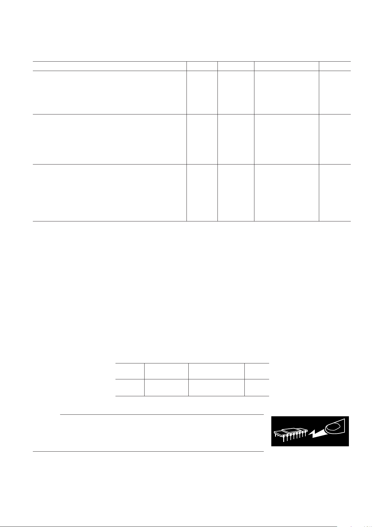
AD9853–SPECIFICATIONS
Parameter Temp Test Level Min Typ Max Units
REF CLOCK INPUT CHARACTERISTICS
Frequency Range
6× REFCLK Disabled (+3.3 V Supply) Full IV 42 126 MHz
6× REFCLK Enabled (+3.3 V Supply) Full IV 7 21 MHz
6× REFCLK Disabled (+5 V Supply) Full IV 108 168 MHz
6× REFCLK Enabled (+5 V Supply) Full IV 18 28 MHz
Duty Cycle +25°CIV 40 60 %
Input Capacitance +25°CV 3 pF
Input Impedance +25°C V 100 MΩ
DAC OUTPUT CHARACTERISTICS
Resolution 10 Bits
Full-Scale Output Current +25°C IV 5 10 20 mA
Gain Error +25°C I –10 +10 % FS
Output Offset +25°CI 10 µA
Output Offset Temperature Coefficient Full V 50 nA/°C
Differential Nonlinearity +25°C I 0.5 0.75 LSB
Integral Nonlinearity +25°C I 0.5 1.5 LSB
Output Capacitance +25°CV 5 pF
Phase Noise @ 1 kHz Offset, 40 MHz A
OUT
6× REFCLK Enabled +25°C V –100 dBc
6× REFCLK Disabled +25°C V –110 dBc
Voltage Compliance Range +25°C I –0.5 +1.5 V
Wideband SFDR (Single Tone):
1 MHz A
OUT
+25°C IV 62 68 dBc
20 MHz A
OUT
+25°C IV 52 54 dBc
42 MHz A
OUT
+25°C IV 48 50 dBc
65 MHz A
OUT
1
+25°C IV 42 44 dBc
MODULATOR CHARACTERISTICS
I/Q Offset +25°CIV 48 dB
Adjacent Channel Power +25°C IV 44 dBm
Error Vector Magnitude +25°CIV 1 2 %
In-Band Spurious Emission
5 MHz–42 MHz A
OUT
+25°C IV 42 dBc
5 MHz–65 MHz A
OUT
1
+25°C IV 40 dBc
Passband Amplitude Ripple +25°CV ±0.3 dB
TIMING CHARACTERISTICS
Serial Control Bus
Maximum Frequency Full IV 25 MHz
Minimum Clock Pulsewidth Low (t
PWL
) Full IV 10 ns
Minimum Clock Pulsewidth High (t
PWH
) Full IV 10 ns
Maximum Clock Rise/Fall Time Full IV 100 ns
Minimum Data Setup Time (t
DS
) Full IV 10 ns
Minimum Data Hold Time (t
DH
) Full IV 10 ns
Minimum Clock Setup—Stop Condition (t
CS
) Full IV 10 ns
Minimum Clock Hold—Start Condition (t
CH
) Full IV 10 ns
RESET
Minimum T
X
ENABLE Low to RESET Low (tTR) Full IV 10 ns
Minimum RESET High to Start Condition (t
RH
) Full IV 10 ns
FEC ENABLE
Minimum FEC ENABLE/DISABLE to T
X
ENABLE High (tFH) Full IV 0 ns
Minimum FEC ENABLE/DISABLE to TXENABLE Low (tFL) Full IV 0 ns
(VS = +3.3 V ⴞ 5%, R
SET
= 3.9 k⍀, Reference Clock Frequency = 20.48 MHz with
6ⴛ REFCLK Enabled, Symbol Rate = 2.56 MS/s, ␣ = 0.25, unless otherwise noted)
–3–REV. C
AD9853
CAUTION
ESD (electrostatic discharge) sensitive device. Electrostatic charges as high as 4000 V readily
accumulate on the human body and test equipment and can discharge without detection.
Although the AD9853 features proprietary ESD protection circuitry, permanent damage may
occur on devices subjected to high energy electrostatic discharges. Therefore, proper ESD
precautions are recommended to avoid performance degradation or loss of functionality.
Parameter Temp Test Level Min Typ Max Units
TIMING CHARACTERISTICS (Continued)
Wake-Up Time–PLL Power-Down +25°CIV 1 ms
Wake-Up Time–DAC Power-Down +25°C IV 200 µs
Wake-Up Time–Digital Power-Down +25°CIV 5 µs
Data Latency (t
DL
) +25°C IV 6 Symbols
Minimum RESET Pulsewidth Low (t
RL
) +25°CIV 10 ns
CMOS LOGIC INPUTS
Logic “1” Voltage, +5 V Supply +25°C I +3.5 V
Logic “1” Voltage, +3.3 V Supply +25°C I +3.0 V
Logic “0” Voltage +25°C I +0.4 V
Logic “1” Current +25°CI 12 µA
Logic “0” Current +25°CI 12 µA
Input Capacitance +25°CV 3 pF
POWER SUPPLY
2
+VS Current (+3.3 V + 5%)
Full Operating Conditions +25°C I 184 230 mA
With PLL Power-Down Enabled +25°C I 178 224 mA
With DAC Power-Down Enabled +25°C I 170 216 mA
With Digital Power-Down Enabled +25°C I 36 54 mA
With All Power-Down Enabled +25°C I 16 20 mA
+V
S
Current (+5 V + 5%) +25°C I 400 595 mA
NOTES
1
Reference clock = 28 MHz with clock multiplier enabled; supply voltage = +5 V.
2
Maximum values are obtained under worst case operating modes. Typical values are valid for most applications.
Specifications subject to change without notice.
EXPLANATION OF TEST LEVELS
Test Level
I – 100% Production Tested.
III – Sample Tested Only.
IV – Parameter is guaranteed by design and characterization
testing.
V – Parameter is a typical value only.
VI – Devices are 100% production tested at +25°C and
guaranteed by design and characterization testing for
industrial operating temperature range.
ABSOLUTE MAXIMUM RATINGS*
Maximum Junction Temperature . . . . . . . . . . . . . . . +150°C
V
S
. . . . . . . . . . . . . . . . . . . . . . . . . . . . . . . . . . . . . . . . . +6 V
Digital Inputs . . . . . . . . . . . . . . . . . . . . . . . . . –0.7 V to +V
S
Digital Output Current . . . . . . . . . . . . . . . . . . . . . . . . . 5 mA
Storage Temperature . . . . . . . . . . . . . . . . . . –65°C to +150°C
Operating Temperature . . . . . . . . . . . . . . . . . –40°C to +85°C
Lead Temperature (10 sec Soldering) . . . . . . . . . . . . +300°C
MQFP θ
JA
Thermal Impedance . . . . . . . . . . . . . . . . . 36°C/W
*Absolute maximum ratings are limiting values, to be applied individually, and
beyond which the serviceability of the circuit may be impaired. Functional
operability under any of these conditions is not necessarily implied. Exposure of
absolute maximum rating conditions for extended periods of time may affect device
reliability.
WARNING!
ESD SENSITIVE DEVICE
ORDERING GUIDE
Temperature Package Package
Model Range Description Option
AD9853AS –40°C to +85°C Metric Quad Flatpack S-44A
(MQFP)

AD9853
–4–
REV. C
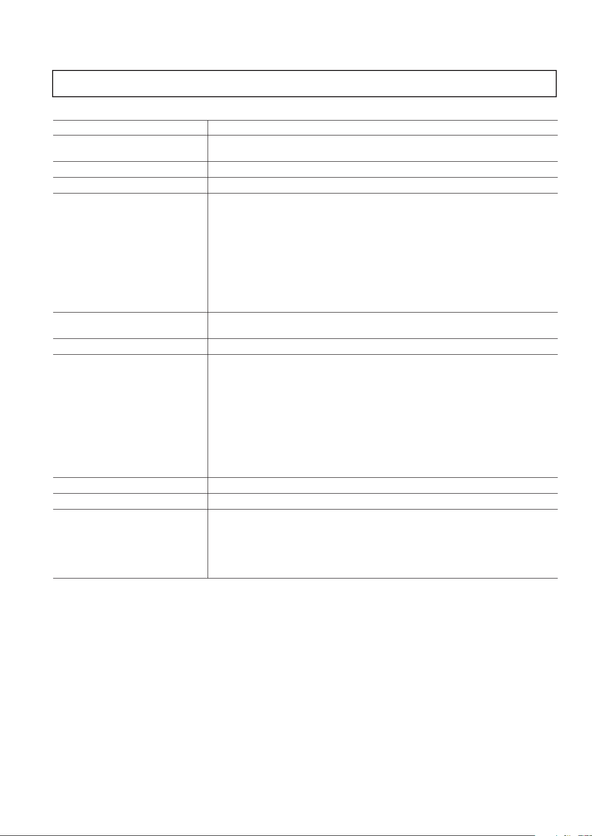
PIN FUNCTION DESCRIPTIONS
Pin # Pin Name Pin Function
1, 7, 9, 10,
36, 39, 44 DGND Digital Ground
2, 8, 37,
40, 43 DVDD Digital Supply Voltage
3 Control Bus Clock Bit Clock for Control Bus
Data
4 Control Bus Data In Control Bus Data In
5 FEC Enable Enables/Disables FEC
6 Address Bit Address Bit for Control Bus
11, 26, 31 Test Data Out Factory Use—Serial Test Data
Out
12, 13 PLL GND PLL Ground
14 PLL VCC Supply Voltage for PLL
15 PLL Filter PLL Loop Filter Connection
16, 19, 23 AGND Analog Ground
17 NC No Connect
18 DAC Rset Rset Resistor Connection
20, 22 AVDD Analog Supply Voltage
21 DAC Baseline DAC Baseline Voltage
24 IOUT Analog Current Output of the
DAC
25 IOUTB Complementary Analog Cur-
rent Output of the DAC
27 Test CLK Factory Use—Scan Clock
28 Test Latch Factory Use—Scan Latch
29 Test Data In Factory Use—Serial Test Data
In
30 Test Data Enable Factory Use—Serial Test Data
Enable, Grounded for Normal
Operation
32 RESET Master Device Reset Function
33 CA Enable Cable Amplifier Enable
34 CA Clock Cable Amplifier Serial Control
Clock
35 CA Data Cable Amplifier Serial Control
Data
38 REF CLK IN Reference Clock Input
41 Data In Input Serial Data Stream
42 T
X
ENABLE Pulse that Frames the Valid
Input Data Stream
PIN CONFIGURATION
44-Lead Metric Quad Flatpack
(S-44A)
3
4
5
6
7
1
2
10
11
8
9
40 39 3841424344 36 35 3437
29
30
31
32
33
27
28
25
26
23
24
PIN 1
IDENTIFIER
TOP VIEW
(Not to Scale)
12 13 14 15 16 171819 20 21 22
AVDD
DAC BASELINE
AVDD
NC
PLL GND
PLL GND
AGND
CA ENABLE
PLL VCC
RESET
TEST DATA OUT
PLL FILTER
TEST DATA
ENABLE
DAC RSET
DVDD
TEST DATA IN
AGND
TEST LATCH
DGND
TEST CLK
IOUTB
AD9853
IOUT
DVDD
AGND
DGND
DGND
DGND
DVDD
CONTROL
BUS CLOCK
DVDD
CONTROL
BUS DATA IN
FEC ENABLE
ADDRESS BIT
DGND
NC = NO CONNECT
DVDD
DGND
DGND
TEST DATA
OUT
TEST DATA OUT
T
X
ENABLE
DATA IN
REF CLK IN
CA CLOCK
CA DATA
ADDRESS BIT
AD9853
–5–REV. C
Table I. Modulator Function Description
Modulation Encoding Format FSK*, QPSK, DQPSK, 16-QAM, D16-QAM, Selectable via Control Bus
Output Carrier Frequency Range DC – 63 MHz with +3.3 V Supply Voltage
DC – 84 MHz with +5 V Supply Voltage
Serial Input Data Rate Evenly Divisible Fraction of Reference Clock
Pulse-Shaping FIR Filter 41 Tap, Linear Phase, 10-Bit Coefficients Fully Programmable via Control Bus
Interpolation Range Interpolation Rate = (4/M) × (ICIC1) × (ICIC2) where: M = 2 for QPSK, M = 4 for 16-QAM
Minimum and Maximum Rates
Minimum Interpolation Rate—QPSK = 2 × 3 × 2 = 12
16-QAM = 1 × 4 × 3 = 12
Maximum Interpolation Rate—QPSK = 2 × 31 × 63 = 3906
16-QAM = 1 × 31 × 63 = 1953
These are the minimum and maximum interpolation ratios from the input data rate to the
system clock. The interpolation range is a function of the fixed interpolation factor of four
in the FIR filters, the programmed CIC filter interpolation rates (ICIC1, ICIC2), as well
as system timing constraints.
Maximum Reference Clock Frequency +3.3 V Supply: 21 MHz with 6× REFCLK enabled, 126 MHz with 6× REFCLK disabled
+5 V Supply: 28 MHz with 6× REFCLK enabled, 168 MHz with 6× REFCLK disabled
6× REFCLK Fixed 6× reference clock multiplier, enable/disable control via control bus
R-S FEC Enable/disable via control bus and dedicated control pin. Control pin enable/disable function:
Logic “1” = Enable
Logic “0” = Disable
Primitive Polynomial: p(x) = x
8
+ x4 + x3 + x2 + 1
Code Generator Polynomial: g(x) = (x + α
0
)(x + α1)(x + α2) . . . (x + α
2t –1
)
Selectable via Control Bus
t = 0–10 (Programmable)
Codeword Length (N) = 255 max (Programmable)
N = K + 2 t (K Range = 16 ≤ K ≤ 255 – 2 t)
FEC/Randomizer can be transposed in signal chain via control bus.
I/Q Channel Spectrum I × COS + Q × SIN (default) or I × COS – Q × SIN, selectable via control bus.
Preamble Insertion 0–96 Bits, Programmable Length and Content
Randomizer Enable/Disable Control via Control Bus
Generating Polynomial:
x
6
+ x5 + 1, Programmable Seed (Davic/DVB-Compliant)
or
x
15
+ x14 + 1, Programmable Seed (DOCSIS-Compliant)
Randomizer and FEC blocks can be transposed in signal chain, via control bus.
*In FSK mode, F0:F1 are direct DDS Cosine output. The two interpolator stages of the AD9853 are not used in the FSK mode and should be programmed for
maximum interpolation rates to reduce unnecessary current consumption. This means that Interpolator #1 should be set to a decimal value of 31, and Interpolator
#2 should be set to decimal value of 63. This is easily accomplished by programming Registers 12 and 13 (hex) with the values of FF (hex).
AD9853
–6–
REV. C
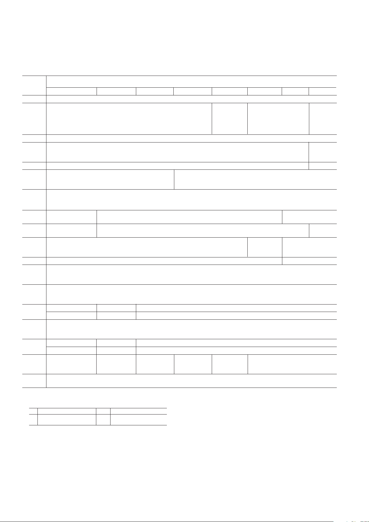
Table II. Control Register Functional Assignment
Register
Address
DATA
(Note 1) D7 D6 D5 D4 D3 D2 D1 D0
00h MSB Value of K (Message Length in Bytes) for Reed-Solomon Encoder, where 16
10
≤ K ≤ 255
10
(Note 2) LSB
01h MSB The Number of Correctable Byte LSB Randomizer Randomizer Length (Note 3)
Errors (t) for the Reed-Solomon Insertion 002 = 6 Bit
Encoder, where 0 ≤ t ≤ 10
10
.01
2
= 15 Bit
For t = 0, the RS encoder is 0 = After RS 102 = Randomizer OFF
effectively disabled. 1 = Before RS 112 = Randomizer OFF
02h MSB Lower Eight Bits of Seed Value for 15-Bit Randomizer (Not Used for 6-Bit Randomizer) LSB
03h MSB Upper Seven Bits of Seed Value for 15-Bit Randomizer LSB
– OR –
Seed Value for 6-Bit Randomizer (D1 not used in this case).
04h MSB Preamble Length (L) where 0 ≤ L ≤ 96 Bits (Note 4) LSB
05h Modulation Mode
0002 = QPSK , 0012 = DQPSK, 0102 = 16-QAM
0112 = D16-QAM , 1002 = FSK
06h The MSB of the preamble always resides in D7 of Address 11h and is the first preamble bit to be clocked out of the device during transmission of
: a packet. Up to 96 bits of preamble are available as specified in Register 04h. Unused bits are don’t care for L < 96.
11h MSB Preamble Data. (Note 5)
12h MSB Interpolator #1: RATE LSB
Rate Change Factor (R) where 3
10
≤ R ≤ 31
10
13h MSB Interpolator #2: RATE LSB
Rate Change Factor (R) where 2
10
≤ R ≤ 63
10
14h MSB Interpolator #1: SCALE LSB 2× Multiplier
0 = OFF
1 = ON
15h
6
MSB Interpolator #2: SCALE LSB
16h Frequency Tuning Word #1 LSB
: FSK Mode: Specifies the “space” frequency (F0).
19h MSB All Other Modes: Specifies the carrier frequency.
1Ah Frequency Tuning Word #2 LSB
: FSK Mode: Specifies the “mark” frequency (F1).
1Dh MSB (Addresses 1Ah–1Dh are only valid for FSK mode.)
1Eh
5
MSB-2 MSB-3 10-Bit FIR End Tap Coefficient, a
0
LSB
0
1Fh MSB
0
MSB-1 <
— —␣ —␣ —␣ —␣ —␣ —␣ —␣ —␣ —␣ —␣ —␣ —␣ —
␣ Unused Bits
—␣ —␣ —␣ —␣ —␣ —␣ —␣ —␣ —␣ —␣ —␣ —␣ —␣ —
>
:
: FIR Intermediate Tap Coefficients, a1 – a
19
:
46h MSB-2 MSB-3 10-Bit FIR Center Tap Coefficient, a
20
LSB
20
47h MSB
20
MSB-1 <
— —␣ —␣ —␣ —␣ —␣ —␣ —␣ —␣ —␣ —␣ —␣ —␣ —
␣ Unused Bits
—␣ —␣ —␣ —␣ —␣ —␣ —␣ —␣ —␣ —␣ —␣ —␣ —␣ —
>
Spectrum Digital Power 6× RefClk PLL Mode DAC Mode
48h 0 = I × Cos + Q × Sin 0 = Normal 0 = Off 0 = Awake 0 = Awake
(Note 7) 1 = I × Cos – Q × Sin 1 = Shutdown 1 = On 1 = Sleep 1 = Sleep
49h AD8320 Cable Driver Gain Control Byte (GCB)
(Note 8) MSB The absolute gain, AV, of the AD8320 is given by: A
V
= 0.316 + 0.077 × GCB (where 0 ≤ GCB ≤ 255
10
) LSB
NOTES
1
The 8-bit Register Address is preceded by an 8-bit Device Address, which is given by
000001XY, where the value of Bits X and Y are determined as follows:
X Voltage Applied to Pin 6 Y Desired Register Function
0 GND 0 WRITE
1+V
S
1 READ
2
This register must be loaded with a nonzero value even if the RS encoder has been
disabled by setting T = 0 in register 01h.
3
Unused regions are don’t care bit locations.
4
If a preamble is not used this register must be initialized to a value of 0 by the user.
5
Addresses 06h–011h and 1Eh–47h are write only.
6
Readback of register 15h results in a value that is 2× the actual programmed value.
This is a design error in the readback function.
7
Assertion of RESET (Pin 32) sets the contents of this register to 0.
8
Registers 0h–48h may be written to using a single register address followed by a
contiguous data sequence (see Figure 27). Register 49h, however, must be written to
individually; i.e., a separately addressed 8-bit data sequence.
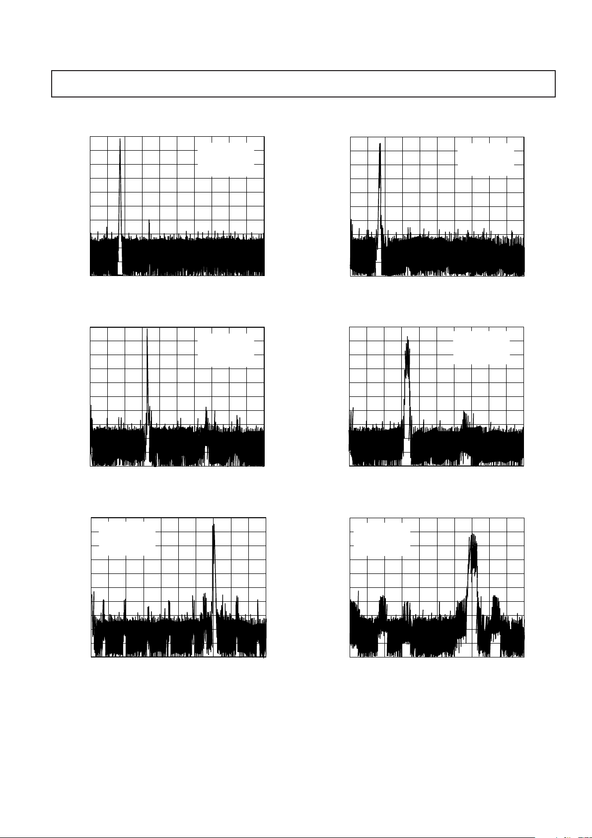
Modulated Output Spectrum with 3.3 V Supply, α = 0.25, 20.48 MHz REFCLK
Typical Performance Characteristics–AD9853
–7–
REV. C
0
–10
–100
START 0Hz
STOP 60MHz
6MHz/
–40
–70
–80
–90
–20
–30
–60
–50
RBW = 3kHz
VBW = 3kHz
SWT = 17s
RF ATT = 10dB
REF LVL = –20dBm
Figure 1. QPSK, 320 kb/s, A
OUT
= 10 MHz
0
–10
–100
START 0Hz
STOP 60MHz
6MHz/
–40
–70
–80
–90
–20
–30
–60
–50
RBW = 3kHz
VBW = 3kHz
SWT = 17s
RF ATT = 10dB
REF LVL = –20dBm
Figure 2. QPSK, 640 kb/s, A
OUT
= 20 MHz
0
–10
–100
START 0Hz
STOP60 MHz
6MHz/
–40
–70
–80
–90
–20
–30
–60
–50
RBW = 3kHz
VBW = 3kHz
SWT = 17s
RF ATT = 10dB
REF LVL = –20dBm
Figure 3. QPSK, 1.28 Mb/s, A
OUT
= 42 MHz
0
–10
–100
START 0Hz
STOP 60MHz
6MHz/
–40
–70
–80
–90
–20
–30
–60
–50
RBW = 3kHz
VBW = 3kHz
SWT = 17s
RF ATT = 10dB
REF LVL = –20dBm
Figure 4. QPSK, 1.28 Mb/s, A
OUT
= 10 MHz
0
–10
–100
START 0Hz
STOP 60MHz
6MHz/
–40
–70
–80
–90
–20
–30
–60
–50
RBW = 3kHz
VBW = 3kHz
SWT = 17s
RF ATT = 10dB
REF LVL = –20dBm
Figure 5. QPSK, 2.56 Mb/s, A
OUT
= 20 MHz
0
–10
–100
START 0Hz
STOP60 MHz
6MHz/
–40
–70
–80
–90
–20
–30
–60
–50
RBW = 3kHz
VBW = 3kHz
SWT = 17s
RF ATT = 10dB
REF LVL = –20dBm
Figure 6. QPSK, 5.12 Mb/s, A
OUT
= 42 MHz
AD9853
–8–
REV. C
0
0
0
0
0
0
0
0
0
0
0
–10
–100
START 0Hz
STOP 60MHz
6MHz/
–40
–70
–80
–90
–20
–30
–60
–50
RBW = 3kHz
VBW = 3kHz
SWT = 17s
RF ATT = 30dB
REF LVL = 0dBm
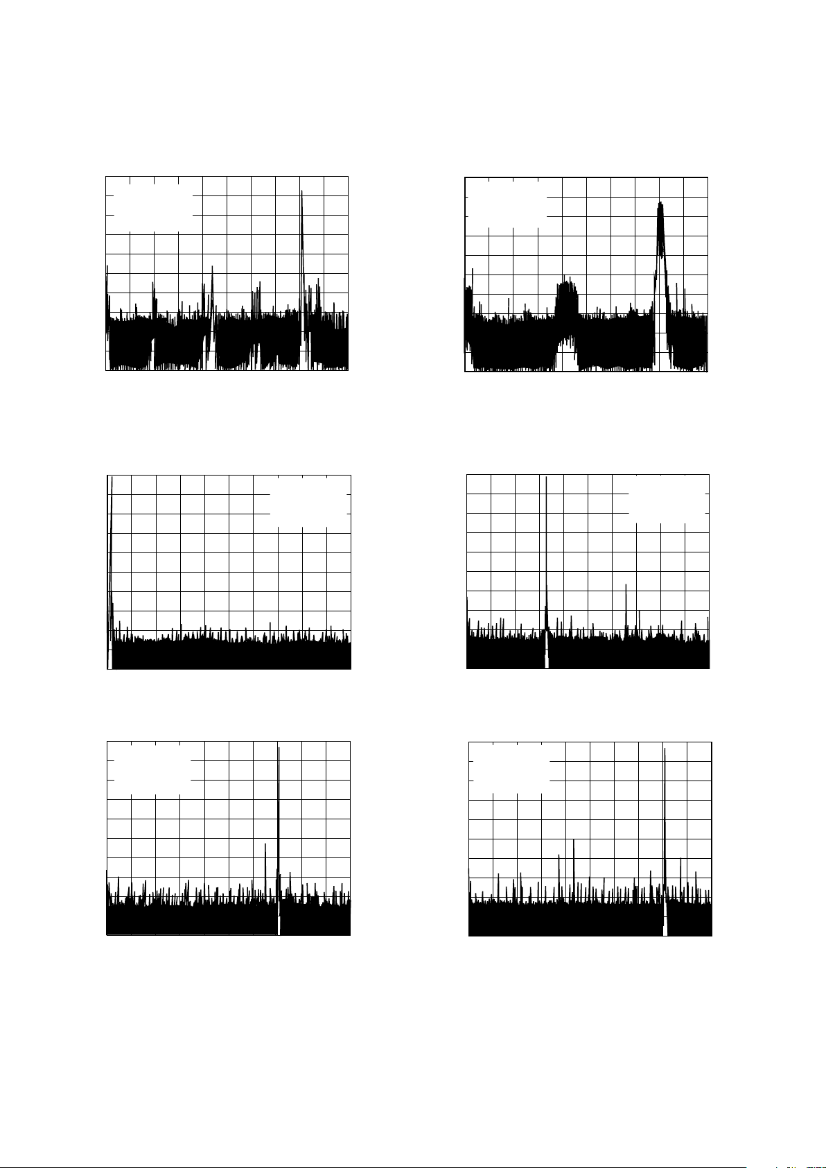
Figure 8. A
OUT
= 1 MHz
0
0
0
0
0
0
0
0
0
0
0
–10
–100
START 0Hz
STOP 60MHz
6MHz/
–40
–70
–80
–90
–20
–30
–60
–50
RBW = 3kHz
VBW = 3kHz
SWT = 17s
RF ATT = 30dB
REF LVL = 0dBm
Figure 9. A
OUT
= 42 MHz
Modulated Output Spectrum with 5 V Supply, ␣ = 0.25, 27.5 MHz REFCLK
0
–10
–10
0
START 0Hz
STOP 80MHz
8MHz/
–40
–70
–80
–90
–20
–30
–60
–50
RBW = 3kHz
VBW = 3kHz
SWT = 22.5s
RF ATT = 10dB
REF LVL = –20dBm
Figure 7. QPSK, 1.375 Mb/s, A
OUT
= 65 MHz
Single Tone Output Spectrum with +3.3 V Supply, 20.48 MHz REFCLK
0
0
0
0
0
0
0
0
0
0
0
–10
–100
START 0Hz
STOP 60MHz
6MHz/
–40
–70
–80
–90
–20
–30
–60
–50
RBW = 3kHz
VBW = 3kHz
SWT = 17s
RF ATT = 30dB
REF LVL = 0dBm
Figure 11. A
OUT
= 20 MHz
0
0
0
0
0
0
0
0
0
0
0
–10
–100
CENTER 40Hz
SPAN 80MHz
8MHz/
–40
–70
–80
–90
–20
–30
–60
–50
RBW = 5kHz
VBW = 5kHz
SWT = 8s
RF ATT = 30dB
REF LVL = 0dBm
Figure 12. A
OUT
= 65 MHz
(+5 V Supply, 27.5 MHz REFCLK)
0
–10
–100
START 0 Hz
STOP 80 MHz
8 MHz/
–40
–70
–80
–90
–20
–30
–60
–50
RBW = 3kHz
VBW = 3kHz
SWT = 22.5s
RF ATT = 10dB
REF LVL = –20dBm
Figure 10. QPSK, 5.5 Mb/s, A
OUT
= 65 MHz
AD9853
–9–REV. C
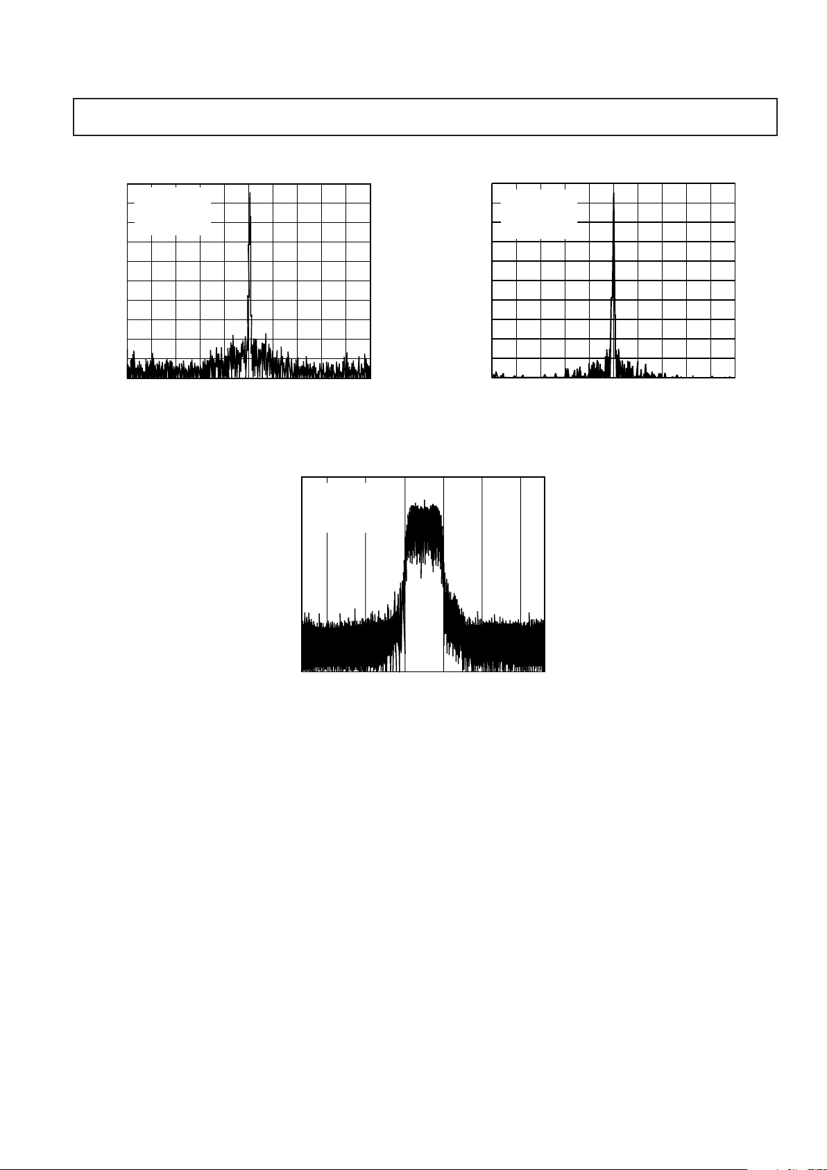
Output Phase Noise Plots, A
OUT
= 40 MHz
0
–10
–100
CENTER 40Hz
SPAN 10MHz
1kHz/
–40
–70
–80
–90
–20
–30
–60
–50
RBW = 30Hz
VBW = 30Hz
SWT = 56s
RF ATT = 20dB
REF LVL = –1dBm
Figure 13. 6ⴛ REFCLK Enabled
CH PWR = –6.98dBm
ACP UP = –44.95dBm
ACP LOW = –44.66dBm
ALT1 UP = –65.96dBm
ALT1 LOW = –65.99dBm
Figure 15. Adjacent Channel Power, A
OUT
= 30 MHz,
2.56 MS/s, Channel BW = 3.2 MHz (
α
= 0.25)
0
–10
–100
CENTER 40Hz
SPAN 10kHz
1kHz/
–40
–70
–80
–90
–20
–30
–60
–50
RBW = 30Hz
VBW = 30Hz
SWT = 56s
RF ATT = 20dB
REF LVL = –1dBm
Figure 14. 6ⴛ REFCLK Disabled
AD9853
–10–
REV. C
SYMBOLS
1.2
–1.2
0
T1
3
REF LVL
–8dBm
CF 42MHz MEAS SIGNAL
SR 1.28MHz EYE [1]
DEMOD 16QAM
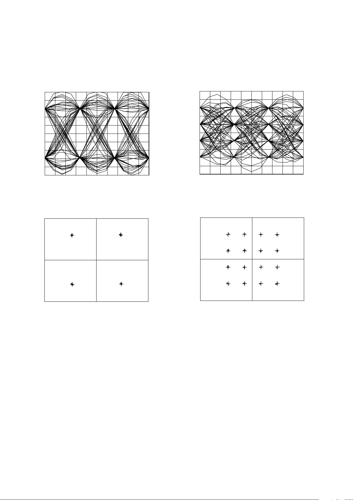
Figure 18. 16-QAM Modulation
1.2
–1.2
–1.5
1.5
REAL
T1
REF LVL
–8dBm
CF 42MHz MEAS SIGNAL
SR 1.28MHz CONSTELLATION
DEMOD 16QAM
Figure 19. 16-QAM Modulation
SYMBOLS
1.2
–1.2
0
T1
3
REF LVL
–7dBm
CF 42MHz MEAS SIGNAL
SR 1.28MHz EYE [1]
DEMOD QPSK
Figure 16. QPSK Modulation
1.2
–1.2
–1.5
1.5
REAL
T1
REF LVL
–7dBm
CF 42MHz MEAS SIGNAL
SR 1.28MHz CONSTELLATION
DEMOD QPSK
Figure 17. QPSK Modulation
Typical Plots of Eye Diagrams and Constellations
 Loading...