

现货库存、技术资料、百科信息、热点资讯,精彩尽在鼎好!
Programmable Digital
a
FEATURES
Universal Low Cost Solution for HFC Network
Return-Channel TX Function: 5 MHz–42 MHz/
5 MHz–65 MHz
165 MHz Internal Reference Clock Capability
Includes Programmable Pulse-Shaping FIR Filters and
Programmable Interpolating Filters
FSK/QPSK/DQPSK/16-QAM/D16-QAM Modulation
Formats
6ⴛ Internal Reference Clock Multiplier
Integrated Reed-Solomon FEC Function
Programmable Randomizer/Preamble Function
Supports Interoperable Cable Modem Standards
Internal SINx/x Compensation
>50 dB SFDR @ 42 MHz Output Frequency (Single Tone)
Controlled Burst Mode Operation
+3.3 V to +5 V Single Supply Operation
Low Power: 750 mW @ Full Clock Speed (3.3 V Supply)
Space Saving Surface Mount Packaging
APPLICATIONS
HFC Data, Telephony and Video Modems
Wireless LAN
QPSK/16-QAM Modulator
AD9853
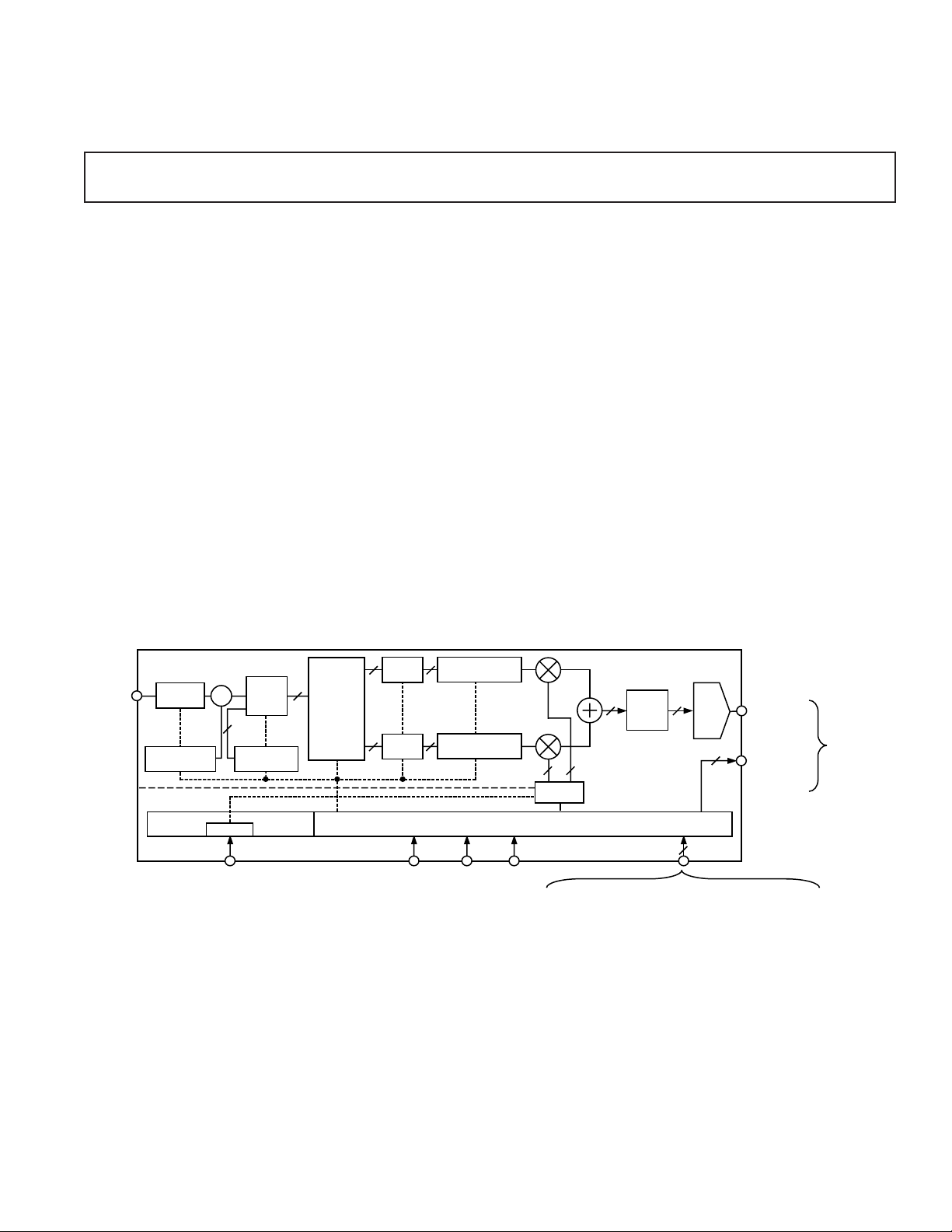
GENERAL DESCRIPTION
The AD9853 integrates a high speed direct-digital synthesizer
(DDS), a high performance, high speed digital-to-analog converter (DAC), digital filters and other DSP functions onto a
single chip, to form a complete and flexible digital modulator
device. The AD9853 is intended to function as a modulator in
network applications such as interactive HFC, WLAN and
MMDS, where cost, size, power dissipation, functional integration and dynamic performance are critical attributes.
The AD9853 is fabricated on an advanced CMOS process and
it sets a new standard for CMOS digital modulator performance.
The device is loaded with programmable functionality and
provides a direct interface port to the AD8320, digitallyprogrammable cable driver amplifier. The AD9853/AD8320
chipset forms a highly integrated, low power, small footprint
and cost-effective solution for the HFC return-path requirement
and other more general purpose modulator applications.
The AD9853 is available in a space saving surface mount package and is specified to operate over the extended industrial
temperature range of –40°C to +85°C.
SERIAL
DATA IN
R-S
FEC
RANDOMIZER
CLOCK
REF CLOCK IN
XOR
63
DATA
DELAY
& MUX
PREAMBLE
INSERTION
ENCODER:
FSK
QPSK
DQPSK
16-QAM
D16-QAM
FUNCTIONAL BLOCK DIAGRAM
INTERPOLATION
FIR
FILTER
FIR
FILTER
FEC
ENABLE/
DISABLE
FILTER
INTERPOLATION
FILTER
CONTROL FUNCTIONS
RESET
ENABLE
T
X
SINE COSINE
DDS
SERIAL CONTROL BUS:
32-BIT OUTPUT FREQUENCY TUNING WORD
INPUT DATA RATE/MODULATION FORMAT
FEC/RANDOMIZER/PREAMBLE ENABLE/CONFIGURATION
FIR FILTER COEFFICIENTS
REF CLOCK MULTIPLIER ENABLE
I/Q PHASE INVERT
SLEEP MODE
AD9853
INV
SYNC
FILTER
10 10
10-BIT
DAC
A
OUT
GAIN
CONTROL TO
DRIVER AMP
TO LP FILTER
AND AD8320
CABLE DRIVER
AMPLIFER
REV. C
Information furnished by Analog Devices is believed to be accurate and
reliable. However, no responsibility is assumed by Analog Devices for its
use, nor for any infringements of patents or other rights of third parties
which may result from its use. No license is granted by implication or
otherwise under any patent or patent rights of Analog Devices.
One Technology Way, P.O. Box 9106, Norwood, MA 02062-9106, U.S.A.
Tel: 781/329-4700 World Wide Web Site: http://www.analog.com
Fax: 781/326-8703 © Analog Devices, Inc., 1999

AD9853–SPECIFICATIONS
(VS = +3.3 V ⴞ 5%, R
6ⴛ REFCLK Enabled, Symbol Rate = 2.56 MS/s, ␣ = 0.25, unless otherwise noted)
= 3.9 k⍀, Reference Clock Frequency = 20.48 MHz with
SET
Parameter Temp Test Level Min Typ Max Units
REF CLOCK INPUT CHARACTERISTICS
Frequency Range
6× REFCLK Disabled (+3.3 V Supply) Full IV 42 126 MHz
6× REFCLK Enabled (+3.3 V Supply) Full IV 7 21 MHz
6× REFCLK Disabled (+5 V Supply) Full IV 108 168 MHz
6× REFCLK Enabled (+5 V Supply) Full IV 18 28 MHz
Duty Cycle +25°CIV 40 60 %
Input Capacitance +25°CV 3 pF
Input Impedance +25°C V 100 MΩ
DAC OUTPUT CHARACTERISTICS
Resolution 10 Bits
Full-Scale Output Current +25°C IV 5 10 20 mA
Gain Error +25°C I –10 +10 % FS
Output Offset +25°CI 10 µA
Output Offset Temperature Coefficient Full V 50 nA/°C
Differential Nonlinearity +25°C I 0.5 0.75 LSB
Integral Nonlinearity +25°C I 0.5 1.5 LSB
Output Capacitance +25°CV 5 pF
Phase Noise @ 1 kHz Offset, 40 MHz A
OUT
6× REFCLK Enabled +25°C V –100 dBc
6× REFCLK Disabled +25°C V –110 dBc
Voltage Compliance Range +25°C I –0.5 +1.5 V
Wideband SFDR (Single Tone):
1 MHz A
OUT
20 MHz A
42 MHz A
65 MHz A
OUT
OUT
OUT
1
+25°C IV 62 68 dBc
+25°C IV 52 54 dBc
+25°C IV 48 50 dBc
+25°C IV 42 44 dBc
MODULATOR CHARACTERISTICS
I/Q Offset +25°CIV 48 dB
Adjacent Channel Power +25°C IV 44 dBm
Error Vector Magnitude +25°CIV 1 2 %
In-Band Spurious Emission
5 MHz–42 MHz A
5 MHz–65 MHz A
OUT
OUT
1
+25°C IV 42 dBc
+25°C IV 40 dBc
Passband Amplitude Ripple +25°CV ±0.3 dB
TIMING CHARACTERISTICS
Serial Control Bus
Maximum Frequency Full IV 25 MHz
Minimum Clock Pulsewidth Low (t
Minimum Clock Pulsewidth High (t
) Full IV 10 ns
PWL
) Full IV 10 ns
PWH
Maximum Clock Rise/Fall Time Full IV 100 ns
Minimum Data Setup Time (t
Minimum Data Hold Time (t
Minimum Clock Setup—Stop Condition (t
Minimum Clock Hold—Start Condition (t
) Full IV 10 ns
DS
) Full IV 10 ns
DH
) Full IV 10 ns
CS
) Full IV 10 ns
CH
RESET
Minimum T
Minimum RESET High to Start Condition (t
ENABLE Low to RESET Low (tTR) Full IV 10 ns
X
) Full IV 10 ns
RH
FEC ENABLE
Minimum FEC ENABLE/DISABLE to T
ENABLE High (tFH) Full IV 0 ns
X
Minimum FEC ENABLE/DISABLE to TXENABLE Low (tFL) Full IV 0 ns
–2–
REV. C
AD9853
WARNING!
ESD SENSITIVE DEVICE
Parameter Temp Test Level Min Typ Max Units
TIMING CHARACTERISTICS (Continued)
Wake-Up Time–PLL Power-Down +25°CIV 1 ms
Wake-Up Time–DAC Power-Down +25°C IV 200 µs
Wake-Up Time–Digital Power-Down +25°CIV 5 µs
Data Latency (t
Minimum RESET Pulsewidth Low (t
CMOS LOGIC INPUTS
Logic “1” Voltage, +5 V Supply +25°C I +3.5 V
Logic “1” Voltage, +3.3 V Supply +25°C I +3.0 V
Logic “0” Voltage +25°C I +0.4 V
Logic “1” Current +25°CI 12 µA
Logic “0” Current +25°CI 12 µA
Input Capacitance +25°CV 3 pF
POWER SUPPLY
+VS Current (+3.3 V + 5%)
Full Operating Conditions +25°C I 184 230 mA
With PLL Power-Down Enabled +25°C I 178 224 mA
With DAC Power-Down Enabled +25°C I 170 216 mA
With Digital Power-Down Enabled +25°C I 36 54 mA
With All Power-Down Enabled +25°C I 16 20 mA
+V
Current (+5 V + 5%) +25°C I 400 595 mA
S
NOTES
1
Reference clock = 28 MHz with clock multiplier enabled; supply voltage = +5 V.
2
Maximum values are obtained under worst case operating modes. Typical values are valid for most applications.
Specifications subject to change without notice.
) +25°C IV 6 Symbols
DL
2
) +25°CIV 10 ns
RL
EXPLANATION OF TEST LEVELS
Test Level
I – 100% Production Tested.
III – Sample Tested Only.
IV – Parameter is guaranteed by design and characterization
testing.
V – Parameter is a typical value only.
VI – Devices are 100% production tested at +25°C and
guaranteed by design and characterization testing for
industrial operating temperature range.
ABSOLUTE MAXIMUM RATINGS*
Maximum Junction Temperature . . . . . . . . . . . . . . . +150°C
V
. . . . . . . . . . . . . . . . . . . . . . . . . . . . . . . . . . . . . . . . . +6 V
S
Digital Inputs . . . . . . . . . . . . . . . . . . . . . . . . . –0.7 V to +V
Digital Output Current . . . . . . . . . . . . . . . . . . . . . . . . . 5 mA
Storage Temperature . . . . . . . . . . . . . . . . . . –65°C to +150°C
Operating Temperature . . . . . . . . . . . . . . . . . –40°C to +85°C
Lead Temperature (10 sec Soldering) . . . . . . . . . . . . +300°C
MQFP θ
*Absolute maximum ratings are limiting values, to be applied individually, and
beyond which the serviceability of the circuit may be impaired. Functional
operability under any of these conditions is not necessarily implied. Exposure of
absolute maximum rating conditions for extended periods of time may affect device
reliability.
Thermal Impedance . . . . . . . . . . . . . . . . . 36°C/W
JA
ORDERING GUIDE
Temperature Package Package
Model Range Description Option
AD9853AS –40°C to +85°C Metric Quad Flatpack S-44A
(MQFP)
CAUTION
ESD (electrostatic discharge) sensitive device. Electrostatic charges as high as 4000 V readily
accumulate on the human body and test equipment and can discharge without detection.
Although the AD9853 features proprietary ESD protection circuitry, permanent damage may
occur on devices subjected to high energy electrostatic discharges. Therefore, proper ESD
precautions are recommended to avoid performance degradation or loss of functionality.
S
–3–REV. C
AD9853
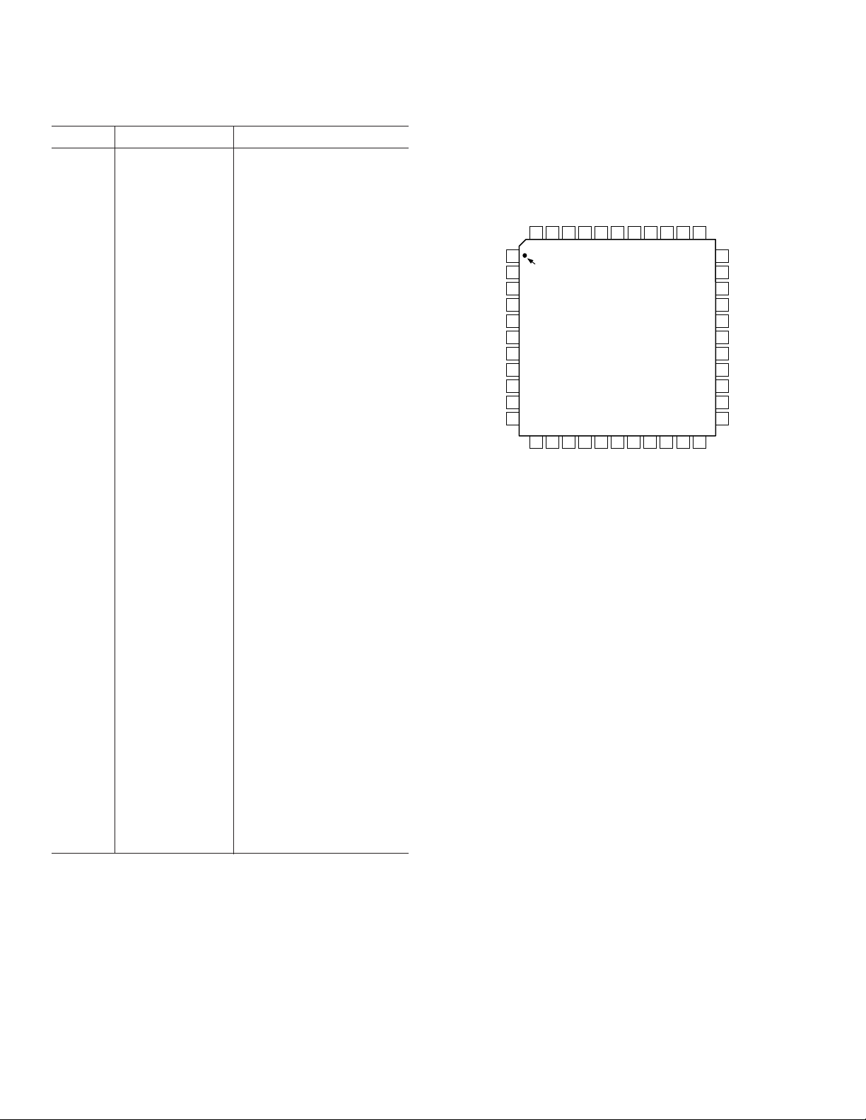
PIN FUNCTION DESCRIPTIONS
Pin # Pin Name Pin Function
1, 7, 9, 10,
36, 39, 44 DGND Digital Ground
2, 8, 37,
40, 43 DVDD Digital Supply Voltage
3 Control Bus Clock Bit Clock for Control Bus
Data
4 Control Bus Data In Control Bus Data In
5 FEC Enable Enables/Disables FEC
6 Address Bit Address Bit for Control Bus
11, 26, 31 Test Data Out Factory Use—Serial Test Data
Out
12, 13 PLL GND PLL Ground
14 PLL VCC Supply Voltage for PLL
15 PLL Filter PLL Loop Filter Connection
16, 19, 23 AGND Analog Ground
17 NC No Connect
18 DAC Rset Rset Resistor Connection
20, 22 AVDD Analog Supply Voltage
21 DAC Baseline DAC Baseline Voltage
24 IOUT Analog Current Output of the
DAC
25 IOUTB Complementary Analog Cur-
rent Output of the DAC
27 Test CLK Factory Use—Scan Clock
28 Test Latch Factory Use—Scan Latch
29 Test Data In Factory Use—Serial Test Data
In
30 Test Data Enable Factory Use—Serial Test Data
Enable, Grounded for Normal
Operation
32 RESET Master Device Reset Function
33 CA Enable Cable Amplifier Enable
34 CA Clock Cable Amplifier Serial Control
Clock
35 CA Data Cable Amplifier Serial Control
Data
38 REF CLK IN Reference Clock Input
41 Data In Input Serial Data Stream
42 T
ENABLE Pulse that Frames the Valid
X
Input Data Stream
DGND
DVDD
CONTROL
BUS CLOCK
CONTROL
BUS DATA IN
FEC ENABLE
ADDRESS BIT
ADDRESS BIT
DGND
DVDD
DGND
DGND
TEST DATA
OUT
NC = NO CONNECT
PIN CONFIGURATION
44-Lead Metric Quad Flatpack
(S-44A)
ENABLE
X
T
DGND
DVDD
1
PIN 1
IDENTIFIER
2
3
4
5
6
7
8
9
10
11
12 13 14 15 16 171819 20 21 22
PLL GND
PLL GND
DVDD
REF CLK IN
DGND
DATA IN
40 39 3841424344 36 35 3437
AD9853
TOP VIEW
(Not to Scale)
NC
AGND
PLL VCC
PLL FILTER
DAC RSET
DGND
DVDD
AVDD
AGND
CA DATA
CA CLOCK
CA ENABLE
33
32
RESET
TEST DATA OUT
31
TEST DATA
30
ENABLE
TEST DATA IN
29
TEST LATCH
28
TEST CLK
27
TEST DATA OUT
26
IOUTB
25
IOUT
24
AGND
23
AVDD
DAC BASELINE
–4–
REV. C

AD9853
Table I. Modulator Function Description
Modulation Encoding Format FSK*, QPSK, DQPSK, 16-QAM, D16-QAM, Selectable via Control Bus
Output Carrier Frequency Range DC – 63 MHz with +3.3 V Supply Voltage
DC – 84 MHz with +5 V Supply Voltage
Serial Input Data Rate Evenly Divisible Fraction of Reference Clock
Pulse-Shaping FIR Filter 41 Tap, Linear Phase, 10-Bit Coefficients Fully Programmable via Control Bus
Interpolation Range Interpolation Rate = (4/M) × (ICIC1) × (ICIC2) where: M = 2 for QPSK, M = 4 for 16-QAM
Minimum and Maximum Rates
Minimum Interpolation Rate—QPSK = 2 × 3 × 2 = 12
16-QAM = 1 × 4 × 3 = 12
Maximum Interpolation Rate—QPSK = 2 × 31 × 63 = 3906
16-QAM = 1 × 31 × 63 = 1953
These are the minimum and maximum interpolation ratios from the input data rate to the
system clock. The interpolation range is a function of the fixed interpolation factor of four
in the FIR filters, the programmed CIC filter interpolation rates (ICIC1, ICIC2), as well
as system timing constraints.
Maximum Reference Clock Frequency +3.3 V Supply: 21 MHz with 6× REFCLK enabled, 126 MHz with 6× REFCLK disabled
+5 V Supply: 28 MHz with 6× REFCLK enabled, 168 MHz with 6× REFCLK disabled
6× REFCLK Fixed 6× reference clock multiplier, enable/disable control via control bus
R-S FEC Enable/disable via control bus and dedicated control pin. Control pin enable/disable function:
Logic “1” = Enable
Logic “0” = Disable
Primitive Polynomial: p(x) = x
Code Generator Polynomial: g(x) = (x + α
Selectable via Control Bus
t = 0–10 (Programmable)
Codeword Length (N) = 255 max (Programmable)
N = K + 2 t (K Range = 16 ≤ K ≤ 255 – 2 t)
FEC/Randomizer can be transposed in signal chain via control bus.
I/Q Channel Spectrum I × COS + Q × SIN (default) or I × COS – Q × SIN, selectable via control bus.
Preamble Insertion 0–96 Bits, Programmable Length and Content
Randomizer Enable/Disable Control via Control Bus
Generating Polynomial:
6
+ x5 + 1, Programmable Seed (Davic/DVB-Compliant)
x
or
15
+ x14 + 1, Programmable Seed (DOCSIS-Compliant)
x
Randomizer and FEC blocks can be transposed in signal chain, via control bus.
*In FSK mode, F0:F1 are direct DDS Cosine output. The two interpolator stages of the AD9853 are not used in the FSK mode and should be programmed for
maximum interpolation rates to reduce unnecessary current consumption. This means that Interpolator #1 should be set to a decimal value of 31, and Interpolator
#2 should be set to decimal value of 63. This is easily accomplished by programming Registers 12 and 13 (hex) with the values of FF (hex).
8
+ x4 + x3 + x2 + 1
0
)(x + α1)(x + α2) . . . (x + α
2t –1
)
–5–REV. C

AD9853
Table II. Control Register Functional Assignment
Register
Address
DATA
(Note 1) D7 D6 D5 D4 D3 D2 D1 D0
00h MSB Value of K (Message Length in Bytes) for Reed-Solomon Encoder, where 16
≤ K ≤ 255
10
(Note 2) LSB
10
01h MSB The Number of Correctable Byte LSB Randomizer Randomizer Length (Note 3)
Errors (t) for the Reed-Solomon Insertion 002 = 6 Bit
Encoder, where 0 ≤ t ≤ 10
.01
10
= 15 Bit
2
For t = 0, the RS encoder is 0 = After RS 102 = Randomizer OFF
effectively disabled. 1 = Before RS 112 = Randomizer OFF
02h MSB Lower Eight Bits of Seed Value for 15-Bit Randomizer (Not Used for 6-Bit Randomizer) LSB
03h MSB Upper Seven Bits of Seed Value for 15-Bit Randomizer LSB
– OR –
Seed Value for 6-Bit Randomizer (D1 not used in this case).
04h MSB Preamble Length (L) where 0 ≤ L ≤ 96 Bits (Note 4) LSB
05h Modulation Mode
0002 = QPSK , 0012 = DQPSK, 0102 = 16-QAM
0112 = D16-QAM , 1002 = FSK
06h The MSB of the preamble always resides in D7 of Address 11h and is the first preamble bit to be clocked out of the device during transmission of
: a packet. Up to 96 bits of preamble are available as specified in Register 04h. Unused bits are don’t care for L < 96.
11h MSB Preamble Data. (Note 5)
12h MSB Interpolator #1: RATE LSB
Rate Change Factor (R) where 3
≤ R ≤ 31
10
10
13h MSB Interpolator #2: RATE LSB
Rate Change Factor (R) where 2
≤ R ≤ 63
10
10
14h MSB Interpolator #1: SCALE LSB 2× Multiplier
0 = OFF
1 = ON
6
15h
MSB Interpolator #2: SCALE LSB
16h Frequency Tuning Word #1 LSB
: FSK Mode: Specifies the “space” frequency (F0).
19h MSB All Other Modes: Specifies the carrier frequency.
1Ah Frequency Tuning Word #2 LSB
: FSK Mode: Specifies the “mark” frequency (F1).
1Dh MSB (Addresses 1Ah–1Dh are only valid for FSK mode.)
5
1Eh
1Fh MSB
MSB-2 MSB-3 10-Bit FIR End Tap Coefficient, a
0
MSB-1 <
— —␣ —␣ —␣ —␣ —␣ —␣ —␣ —␣ —␣ —␣ —␣ —␣ —
0
␣ Unused Bits
LSB
—␣ —␣ —␣ —␣ —␣ —␣ —␣ —␣ —␣ —␣ —␣ —␣ —␣ —
0
>
:
: FIR Intermediate Tap Coefficients, a1 – a
19
:
46h MSB-2 MSB-3 10-Bit FIR Center Tap Coefficient, a
47h MSB
20
MSB-1 <
— —␣ —␣ —␣ —␣ —␣ —␣ —␣ —␣ —␣ —␣ —␣ —␣ —
20
␣ Unused Bits
—␣ —␣ —␣ —␣ —␣ —␣ —␣ —␣ —␣ —␣ —␣ —␣ —␣ —
LSB
20
>
Spectrum Digital Power 6× RefClk PLL Mode DAC Mode
48h 0 = I × Cos + Q × Sin 0 = Normal 0 = Off 0 = Awake 0 = Awake
(Note 7) 1 = I × Cos – Q × Sin 1 = Shutdown 1 = On 1 = Sleep 1 = Sleep
49h AD8320 Cable Driver Gain Control Byte (GCB)
(Note 8) MSB The absolute gain, AV, of the AD8320 is given by: A
NOTES
1
The 8-bit Register Address is preceded by an 8-bit Device Address, which is given by
000001XY, where the value of Bits X and Y are determined as follows:
X Voltage Applied to Pin 6 Y Desired Register Function
0 GND 0 WRITE
1+V
2
This register must be loaded with a nonzero value even if the RS encoder has been
disabled by setting T = 0 in register 01h.
3
Unused regions are don’t care bit locations.
4
If a preamble is not used this register must be initialized to a value of 0 by the user.
5
Addresses 06h–011h and 1Eh–47h are write only.
S
1 READ
6
Readback of register 15h results in a value that is 2× the actual programmed value.
This is a design error in the readback function.
7
Assertion of RESET (Pin 32) sets the contents of this register to 0.
8
Registers 0h–48h may be written to using a single register address followed by a
contiguous data sequence (see Figure 27). Register 49h, however, must be written to
individually; i.e., a separately addressed 8-bit data sequence.
= 0.316 + 0.077 × GCB (where 0 ≤ GCB ≤ 255
V
) LSB
10
–6–
REV. C
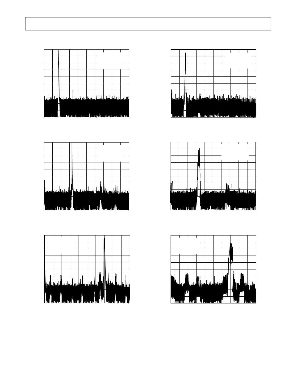
Typical Performance Characteristics–AD9853
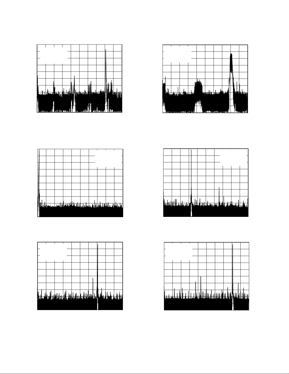
Modulated Output Spectrum with 3.3 V Supply, α = 0.25, 20.48 MHz REFCLK
0
–10
–20
–30
–40
–50
–60
–70
–80
–90
–100
START 0Hz
6MHz/
Figure 1. QPSK, 320 kb/s, A
0
–10
–20
–30
–40
–50
–60
–70
–80
–90
–100
START 0Hz
6MHz/
Figure 2. QPSK, 640 kb/s, A
RBW = 3kHz
VBW = 3kHz
SWT = 17s
RF ATT = 10dB
REF LVL = –20dBm
STOP 60MHz
= 10 MHz
OUT
RBW = 3kHz
VBW = 3kHz
SWT = 17s
RF ATT = 10dB
REF LVL = –20dBm
STOP 60MHz
= 20 MHz
OUT
0
–10
–20
–30
–40
–50
–60
–70
–80
–90
–100
START 0Hz
6MHz/
Figure 4. QPSK, 1.28 Mb/s, A
0
–10
–20
–30
–40
–50
–60
–70
–80
–90
–100
START 0Hz
6MHz/
Figure 5. QPSK, 2.56 Mb/s, A
RBW = 3kHz
VBW = 3kHz
SWT = 17s
RF ATT = 10dB
REF LVL = –20dBm
STOP 60MHz
= 10 MHz
OUT
RBW = 3kHz
VBW = 3kHz
SWT = 17s
RF ATT = 10dB
REF LVL = –20dBm
STOP 60MHz
= 20 MHz
OUT
REV. C
0
RBW = 3kHz
–10
VBW = 3kHz
SWT = 17s
RF ATT = 10dB
–20
REF LVL = –20dBm
–30
–40
–50
–60
–70
–80
–90
–100
START 0Hz
6MHz/
Figure 3. QPSK, 1.28 Mb/s, A
= 42 MHz
OUT
STOP60 MHz
–7–
0
RBW = 3kHz
–10
VBW = 3kHz
SWT = 17s
RF ATT = 10dB
–20
REF LVL = –20dBm
–30
–40
–50
–60
–70
–80
–90
–100
START 0Hz
6MHz/
Figure 6. QPSK, 5.12 Mb/s, A
= 42 MHz
OUT
STOP60 MHz
AD9853
Modulated Output Spectrum with 5 V Supply, ␣ = 0.25, 27.5 MHz REFCLK
0
RBW = 3kHz
–10
VBW = 3kHz
SWT = 22.5s
–20
RF ATT = 10dB
REF LVL = –20dBm
–30
–40
–50
–60
–70
–80
–90
–10
START 0Hz
0
8MHz/
Figure 7. QPSK, 1.375 Mb/s, A
STOP 80MHz
= 65 MHz
OUT
Single Tone Output Spectrum with +3.3 V Supply, 20.48 MHz REFCLK
0
–10
–20
–30
–40
–50
–60
–70
–80
–90
–100
0
0
0
0
0
0
0
0
0
0
START 0Hz
Figure 8. A
6MHz/
OUT
RBW = 3kHz
VBW = 3kHz
SWT = 17s
RF ATT = 30dB
REF LVL = 0dBm
= 1 MHz
STOP 60MHz
0
RBW = 3kHz
VBW = 3kHz
–10
SWT = 22.5s
RF ATT = 10dB
–20
REF LVL = –20dBm
–30
–40
–50
–60
–70
–80
–90
–100
START 0 Hz
Figure 10. QPSK, 5.5 Mb/s, A
0
0
0
–10
0
–20
0
–30
0
–40
0
–50
0
–60
–70
0
0
–80
0
–90
–100
START 0Hz
Figure 11. A
8 MHz/
6MHz/
= 20 MHz
OUT
STOP 80 MHz
= 65 MHz
OUT
RBW = 3kHz
VBW = 3kHz
SWT = 17s
RF ATT = 30dB
REF LVL = 0dBm
STOP 60MHz
–10
–20
–30
–40
–50
–60
–70
–80
–90
–100
0
0
0
0
0
0
0
0
0
0
0
RBW = 3kHz
VBW = 3kHz
SWT = 17s
RF ATT = 30dB
REF LVL = 0dBm
START 0Hz
Figure 9. A
6MHz/
= 42 MHz
OUT
STOP 60MHz
–8–
–10
–20
–30
–40
–50
–60
–70
–80
–90
–100
0
0
0
0
0
0
0
0
0
0
0
CENTER 40Hz
RBW = 5kHz
VBW = 5kHz
SWT = 8s
RF ATT = 30dB
REF LVL = 0dBm
8MHz/
Figure 12. A
= 65 MHz
OUT
(+5 V Supply, 27.5 MHz REFCLK)
SPAN 80MHz
REV. C
AD9853
Output Phase Noise Plots, A
0
RBW = 30Hz
–10
VBW = 30Hz
SWT = 56s
RF ATT = 20dB
–20
REF LVL = –1dBm
–30
–40
–50
–60
–70
–80
–90
–100
CENTER 40Hz
Figure 13. 6ⴛ REFCLK Enabled
1kHz/
= 40 MHz
OUT
SPAN 10MHz
CH PWR = –6.98dBm
ACP UP = –44.95dBm
ACP LOW = –44.66dBm
ALT1 UP = –65.96dBm
ALT1 LOW = –65.99dBm
0
–10
–20
–30
–40
–50
–60
–70
–80
–90
–100
CENTER 40Hz
RBW = 30Hz
VBW = 30Hz
SWT = 56s
RF ATT = 20dB
REF LVL = –1dBm
1kHz/
Figure 14. 6ⴛ REFCLK Disabled
SPAN 10kHz
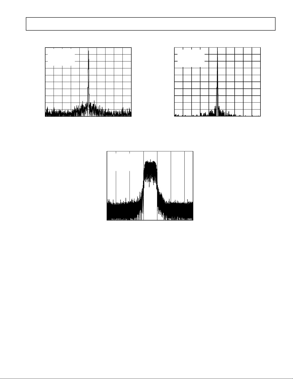
Figure 15. Adjacent Channel Power, A
α
2.56 MS/s, Channel BW = 3.2 MHz (
= 0.25)
= 30 MHz,
OUT
–9–REV. C
AD9853
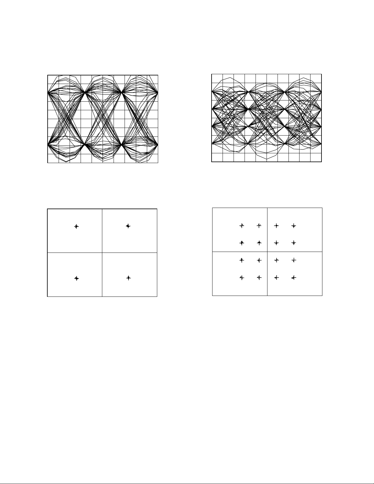
Typical Plots of Eye Diagrams and Constellations
T1
–1.2
1.2
1.2
REF LVL
–7dBm
0
SYMBOLS
Figure 16. QPSK Modulation
REF LVL
–7dBm
SR 1.28MHz CONSTELLATION
CF 42MHz MEAS SIGNAL
SR 1.28MHz EYE [1]
DEMOD QPSK
CF 42MHz MEAS SIGNAL
DEMOD QPSK
REF LVL
–8dBm
1.2
T1
–1.2
3
0
SYMBOLS
CF 42MHz MEAS SIGNAL
SR 1.28MHz EYE [1]
DEMOD 16QAM
3
Figure 18. 16-QAM Modulation
CF 42MHz MEAS SIGNAL
SR 1.28MHz CONSTELLATION
DEMOD 16QAM
1.2
REF LVL
–8dBm
–1.2
T1
–1.5
REAL
Figure 17. QPSK Modulation
1.5
–1.2
T1
–1.5
REAL
Figure 19. 16-QAM Modulation
1.5
–10–
REV. C

AD9853
95
135
140
BIT RATE >2Mb/s
VCC = +5V
CONTINUOUS MODE
145
150
155
160 165
170120
85
75
65
AMBIENT TEMP – 8C
55
45
110
115
130
125
MAX CLOCK RATE – MHz
Figure 20. Max CLK Rate vs. Ambient Temperature
(To Ensure Max Junction Temp is Not Exceeded)
2.6
2.4
2.2
2.0
1.8
POWER – Watts
1.6
VCC = +5.0V
CLK = 165MHz
CONTINUOUS MODE
0.80
CLK = 122.88 MHz
VCC = +3.3V
0.75
CONTINUOUS MODE
0.70
0.65
POWER – Watts
0.60
0.55
01 62345
BIT RATE – Mb/s
Figure 23. PWR Consumption vs. Bit Rate
2.5
CLK = 165MHz
VCC = +5.0V
2.4
BIT RATE = 3.4Mb/s
2.3
2.2
POWER – Watts
2.1
1.4
1.2
0 0.5 3.51.0 1.5 2.0 2.5 3.0
VCC = +4.0V
BIT RATE – Mb/s
Figure 21. Power Consumption vs. Bit Rate
–40
A
= 42MHz
OUT
A
= 32MHz
–45
–50
–55
SPURIOUS IN-BAND EMISSION – dBc
CLK = 122.88 MHz
VCC = +3.3V
–60
5.12 2.56 0.641.28
A
OUT
= 12MHz
BIT RATE – Mb/s
OUT
A
OUT
= 22MHz
Figure 22. Spurious Emission vs. Bit Rate vs. A
OUT
2.0
1.9
0 20 10040 60 80
BURST MODE DUTY CYCLE – %
Figure 24. Power Consumption vs. Burst Duty Cycle
–40
A
= 65MHz
A
OUT
OUT
= 40MHz
OUT
–42
–44
–46
–48
A
= 20MHz
–50
SPURIOUS IN-BAND EMISSION – dBc
CLK = 165MHz
VCC = +4.0V TO +5.0V
–52
3.5 1.75 0.440.88
OUT
BIT RATE – Mb/s
Figure 25. Spurious Emission vs. Bit Rate vs. A
–11–REV. C

AD9853
T
ENABLE
X
DATA IN
INTERNAL CODE-
WORD STRUCTURE
AT R-S OUTPUT
T
ENABLE TO
X
LATENCY
A
OUT
TXENABLE
DATA IN
T
ENABLE
X
FRAME STRUCTURE: MIN TXENABLE LOW TIME = PREAMBLE + 8 SYMBOLS. (EQUATES TO 8 SYMBOLS
NOTE: DATA RATE MUST BE PRECISELY
SYNCHRONIZED WITH RISING EDGE
OF T
D1 D2 D3 D4 D5 D6 D7 DN DON'T CARE D1 D2 D3 D4 D5 D6 D7 DN DON'T CARE
DATA PACKET = K BYTES
FRAME STRUCTURE FOR MULTIPLE CODE WORDS OR CONTINOUS TRANSMISSION:
D1 D2 D3 D4 D5 D6 D7 DN DON'T CARE D1 D2 D3 D4 D5 D6 D7 DN DON'T CARE
DATA PACKET = K BYTES
INPUT DATA PROCESSING:
MINIMUM SPACING BETWEEN BURSTS WITH NO CHANGE IN PROFILE)
ENABLE
X
FEC PARITY
(2T BYTES)
FEC PARITY
(2T BYTES)
DATA PACKET = K BYTES
DATA PACKET = K BYTES
FEC PARITY
(2T BYTES)
ONE CODEWORDONE CODEWORD
FEC PARITY
(2T BYTES)
INTERNAL
BIT CLOCK
DATA IN
ENCODER
INPUT
NOTES ON BURST TRANSMISSION OPERATION:
1. PACKET LENGTH = NUMBER OF INFORMATION BYTES, K
2. IN FEC MODE T
3. IF NECESSARY, ZERO FILL THE LAST CODEWORD TO REACH ASSIGNED K DATA BYTES PER CODEWORD
4. THE INPUT DATA IS SAMPLED AT THE BIT RATE FREQUENCY (f
RISING EDGE OF T
5. PREAMBLE DELAY =
6. DATA RATE MUST BE EXACT SUB-MULTIPLE OF REFERENCE CLOCK.
D1 D59 DND60 D61 D62 D63 D64 D65
D2 D3 D4 D5
PREAMBLE INSERTION
PREAMBLE LENGTH = 96 BITS MAXIMUM
DURING THIS INTERVAL THE DATA IS R-S ENCODED, RANDOMIZED, AND
DELAYED TO SYNCHRONIZE WITH THE END OF THE PREAMBLE DATA.
COMPLETE FRAME AS PRESENTED TO MODULATOR ENCODER:
CODEWORD(S)PREAMBLE
ENABLE MUST BE KEPT HIGH FOR N 3 (K+2T) BYTES WHERE N IS THE NUMBER OF CODEWORDS
X
) WITH THE FIRST SAMPLE TAKEN AT SECONDS AFTER THE
ENABLE
X
(# OF PREAMBLE BITS)
(BIT RATE FREQUENCY)
B
2 3 (f
Figure 26. Data Framing and Processing
D1 D2
DATA
PACKET
AND
FEC PARITY
1
)
B
–12–
REV. C

AD9853
WRITE
S
READ
S
FEC DISABLE/
ENABLE CONTROL
DEVICE ADDRESS A(S)
LSB = 0
DEVICE ADDRESS A(S) REGISTER ADDRESS A(S)
S = START CONDITION
P = STOP CONDITION
REGISTER ADDRESS
A(S) = ACKNOWLEDGE BY SLAVE
A(M) = ACKNOWLEDGE BY MASTER
A(S) DATA A(S)
Figure 27. Serial Control Bus—Read and Write Sequences
MSB
A100000
Figure 28. Serial Control Bus—8-Bit Device Address Detail
LSB = 1
LSB
R/W
0 = WRITE / 1 = READ
ADDRESS CONTROL
(SET VIA DEVICE PIN 6)
DATA A(S) P
DATA
A(M) = NO ACKNOWLEDGE BY MASTER
A(M)
PDEVICE ADDRESS A(S) DATASA(M)
T
ENABLE
X
t
= FEC TO TXENABLE SETUP TIME = 0ns
FH
t
= FEC TO TXENABLE HOLD TIME = 0ns
FL
TXENABLE
RESET
CONTROL CLOCK
CONTROL DATA
t
FH
Figure 29. FEC Enable/Disable Timing Diagram
t
TR
t
RL
t
MP
t
PWH
t
PWL
t
RH
t
t
t
CH
DS
t
= MINIMUM TXENABLE LOW TO RESET LOW = 10ns
TR
t
= MINIMUM RESET PULSEWIDTH = 10ns
RL
t
= MINIMUM RESET TO START CONDITION = 10ns
RH
t
= MINIMUM CLOCK HOLD TIME START CONDITION = 10ns
CH
t
= MINIMUM CLOCK SETUP TIME STOP CONDITION = 10ns
CS
t
= MINIMUM DATA SETUP TIME = 10ns
DS
t
= MINIMUM DATA HOLD TIME = 10ns
DH
t
=
t
t
PWH
MP
= MINIMUM CLOCK PULSEWIDTH HIGH/LOW = 10ns
PWL
= MINIMUM CLOCK PERIOD = 40ns = 25MHz
DH
Figure 30. Serial Control Interface Timing Diagram
t
FL
t
CS
–13–REV. C

AD9853
RESET
t
RL
CONTROL BUS
T
ENABLE
X
DAC OUT
t
: MINIMUM RESET LOW TIME = 10ns
RL
t
: DATA LATENCY = 6 SYMBOLS
DL
NOTE 1. DURING THIS INTERVAL ALL CONTROL BUS REGISTERS MUST BE PROGRAMMED.
NOTE 2. DURING THIS INTERVAL THE CONTROL REGISTER (48h) MAY NEED TO BE REPROGRAMMED DUE TO BEING CLEARED
BY THE PRECEDING RESET PULSE.
NOTE 3. THREE RESETS ARE REQUIRED TO ENSURE THAT THE DATA PATH IS ZERO'D.
NOTE 1
NOTE
2
NOTE
2
Figure 31. Recommended Start-Up Sequence
NOTES ON THE RESET FUNCTION:
1. RESET IS ACTIVE LOW
2. RESET ZEROS THE CONTROL REGISTER AT ADDRESS 48 HEX WHICH CAUSES THE FOLLOWING DEFAULT
CONDITION TO EXIST:
A. 63 REFCLK IS DISABLED
B. OUTPUT SPECTRUM IS SET TO I3COS+Q3SIN
C. DIGITAL PLL POWER-DOWN IS DISABLED
D. PLL POWER-DOWN IS DISABLED
E. DAC PLL POWER-DOWN IS DISABLED
3. SERIAL CONTROL BUS IS RESET AND INITIALIZED.
4. OUTPUTS OF MODULATION ENCODERS ARE SET TO ZERO. THIS ALLOWS THE FIR FILTERS AND
SUBSEQUENT INTERPOLATION FILTERS TO BE FLUSHED WITH ZEROS AS LONG AS T
5. THE PREAMBLE IS CLEARED UPON EXECUTION OF THE RESET FUNCTION.
t
DL
ENABLE IS HELD LOW.
X
START UP
SEQUENCE
DATA IN
REF
CLOCK IN
DIRECT
CONTROL
AD9853
DIGITAL
QPSK/16–QAM
MODULATOR
LINES
CONTROL
CONTROL
CONTROL PROCESSOR
PROCESSOR
SERIAL
BUS
GAIN CONTROL BUS
COUPLING
CIRCUIT AND
LP FILTER
POWER
DOWN
AD8320
PROGRAMMABLE
CABLE DRIVER
AMPLIFIER
TO
DIPLEXER
Figure 32. Basic Implementation of AD9853 Digital Modulator and AD8320 Programmable Cable Driver Amplifier in
Return-Path Application
–14–
REV. C

AD9853
THEORY OF OPERATION
The AD9853 is a highly integrated modulator function that has
been specifically designed to meet the requirements of the HFC
upstream function for both interoperable and proprietary system
implementations. The AD8320 is a companion cable driver
amplifier with a digitally-programmable gain function, that
interfaces to the AD9853 modulator and directly drives the
cable plant with the modulated carrier. Together, the AD9853
and AD8320 provide an easily implementable transmitter solution for the HFC return-path requirement.
CONTROL AND DATA INTERFACE
As shown in the device’s block diagram on the front page, the
various transmit parameters, which include the input data rate,
modulation format, FEC and randomizer configurations, as well
as all the other modulator functions, are programmed into the
AD9853 via a serial control bus. The AD8320 cable driver amp
gain can be programmed directly from the AD9853 via a 3-wire
bus by writing to the appropriate AD9853 register. The AD9853
also contains dedicated pins for FEC enable/disable and a RESET
function.
Note: T
ENABLE pin must be held low for the duration of all
X
serial control bus operations.
The AD9853’s serial control bus consists of a bidirectional data
line and a clock line. Communication is initiated upon a start
condition, which is defined as a high-to-low transition of the
data line while the clock is held high. Communication terminates
upon a stop condition, which is defined as a low-to-high transition in the data line while the clock is held high. Ordinarily, the
data line transitions only while the clock line is low to avoid a
start or stop condition. Data is always written or read back in
8-bit bytes followed by a single acknowledge bit. The microcontroller or ASIC (i.e., the bus master) transfers eight data bits
and the AD9853 (i.e., the slave) issues the acknowledge bit. The
acknowledge bit is active low and is clocked out on every ninth
clock pulse. The bus master must three-state the data line during the ninth clock pulse and allow the AD9853 to pull it low.
A valid write sequence consists of a minimum of three bytes.
This means 27 clock pulses (three bytes with nine clock pulses
each) must be provided by the bus master. The first byte is a
chip address byte that is predefined except for Bit Positions 1
and 0. Bit Positions 7, 6, 5, 4 and 3 must be zero. Bit Position 2
must be a one. Bit 1 is set according to the external address pin
on the AD9853 (1 if the pin is connected to +V
; 0 if the pin
S
is grounded). Bit 0 is set to 1 if a read operation is desired, 0 if a
write operation is desired. The second byte is a register address
with valid addresses between 00h and 49h. An address which is
outside of this range will not be acknowledged. The third byte is
data for the address register. Multiple data bytes are allowed
and loaded sequentially. That is, the first data byte is written to
the addressed register and any subsequent data bytes are written
to subsequent register addresses. It is permissible to write all
registers by issuing a valid chip address byte, then an address
byte of 00h and then 72 (48h) data bytes. Address 49h must be
written independently, that is, not in conjunction with any other
address.
A valid read sequence consists of a minimum of four bytes (refer
to Figure 27). This means the bus master must provide 36 clock
pulses (four bytes with nine clock pulses each). Like the write
sequence, the first two bytes are the Chip Address Byte, with the
read/write bit set to 0, and the readback register address. After
the slave provides an acknowledge at the end of the register
address, the master must present a START condition on the
bus, followed by the Chip Address Byte with the read/write bit
set to a 1. The slave proceeds to provide an acknowledge. During the next eight clocks the slave will write to the bus from the
register address. The master must provide an acknowledge on
the ninth clock of this byte. Any subsequent clocks from the
master will force the slave to read back from subsequent registers. At the end of the read-back cycle, the MASTER must force
a “no-acknowledge” and then a STOP condition. This will take
the SLAVE out of read-back mode. Not all of the serial control
bus registers can be read back. Registers (06h–11h) and (1Eh–
47h) are write only. Also, like the writing procedure, register
49h must be read from independently.
INPUT DATA SYNCHRONIZATION
The serial input data interface consists of two pins, the serial
data input pin and a T
the bit rate and is framed by the T
ENABLE pin. The input data arrives at
X
ENABLE signal as shown in
X
Figure 26. A high frequency sampling clock continuously
samples the T
the rising edge of T
ENABLE signal to detect the rising edge. Once
X
ENABLE is detected, an internal sampler
X
strobes the serial data at the correct point in time relative to the
positive T
ENABLE transition and then continues to sample at
X
the correct interval based on the programmed Input Data rate.
For proper synchronization of the AD9853, 1) the input burst
data must be accurately framed by T
ENABLE and 2) the
X
input data rate must be an exact even submultiple of the system
clock. Typically this will require that the input data rate clock be
synchronized with reference clock.
REED-SOLOMON ENCODER
The AD9853 contains a programmable Reed-Solomon (R-S)
encoder capable of generating an (N, K) code where N is the
code word length and K is the message length.
Error correction becomes vital to reliable communications when
the transmission channel conditions are less than ideal. The
original message can be precisely reconstructed from a corrupted transmission as long as the number of message errors is
within the encoder’s limits. When forward error correction
(FEC) is engaged, either through the serial control interface
bus or hardware (logic high at Pin 5), it is implemented using
the following MCNS-compatible field generator and primitive
polynomials:
Primitive Polynomial: p(x) = x
Code Generator Polynomial: g(x) = (x + a
. . . (x + a
8
+ x4 + x3 + x2 + 1
0
)(x + a1)(x + a2)
2t – 1
)
The code-word structure is defined as follows:
N = K + 2t (bytes)
where:
N = code-word length
K = message length (in bytes), programmable from 16–255
t = number of byte errors that can be corrected programmable
from 0–10.
A Code Word is the sum of the Message Length (in bytes) and
number of Check Bytes required to correct byte errors at the
–15–REV. C

AD9853
receive end. The values actually programmed on the serial control bus are “K” and “t,” which will define N as shown in the
above code-word structure equation. As can be seen from the
code-word structure equation, two check bytes are required to
correct each byte error. Setting t = 0 and K > 0 will bypass the
Reed-Solomon encoding process.
Since Reed-Solomon works on bytes of information and not
bits, a single byte error can be as small as one inverted bit out of
a byte, or as large as eight inverted bits of one byte; in either
instance the result is one byte error. For example, if the value
“t” is specified as 5, the R-S FEC could be correcting as many
as 40, or as few as 05, erroneous bits, but those errors must be
contained in 5 message bytes. If the errors are spread among
more than five bytes, the message will not be fully error corrected.
When using the R-S encoder, the message data needs to be
partitioned or “gapped” with “don’t care” data for the time
duration of the check bytes as shown in the timing diagram of
Figure 26. During the intervals between message data, the device ignores data at the input.
The position of the R-S encoder in the coding data path can be
switched with the randomizer by exercising Register 1, Bit D3,
via the serial control bus.
RANDOMIZER FUNCTION
The next stage in the modulation chain is the randomizing or
“scrambling” stage. Randomizing is necessary due to the fact
that impairments in digital transmission can be a function of the
statistics of the digital source. Receiver symbol synchronization
is more easily maintained if the input sequence appears random
or equiprobable. Long strings of 0s or 1s can cause a bit or
symbol synchronizer to lose synchronization. If there are repetitive patterns in the data, discrete spurs can be produced, causing interchannel interference. In modulation schemes relying on
suppressed carrier transmission, nonrandom data can increase
the carrier feedthrough. Using a randomizer effectively “whitens”
the data.
The technique used in the AD9853 to randomize the data is to
perform a modulo 2 logic addition of the data with a pseudorandom sequence. The pseudorandom sequence is generated by
a shift register of length m with an exclusive OR combination of
the nth bit and the last (mth) bit of the shift register that is fed
back to the shift register input. By choosing the appropriate
feedback point, a maximal length sequence is generated. The
maximal length sequence will repeat after every 2
but appears effectively “random” at the output. The criterion
for maximal length is that the polynomial 1 + x
m
clock cycles,
n
+ xm be irreducible and prime over the Galois field. The AD9853 contains
the following two polynomial configurations in hardware:
15
x
+ x14 +1 :MCNS (DOCSIS) compatible.
6
x
+ x5 +1 :DAVIC/DVB compatible.
The seed value is fully programmable for both configurations.
The seed value is reset prior to each burst and is used to calculate the randomizer bit, which is combined in an exclusive XOR
with the first bit of data from each burst. The first bit of data in
a burst is the MSB of the first symbol following the last symbol
of the internally generated preamble.
PREAMBLE INSERTION BLOCK
As shown in the block diagram of the AD9853, the circuit includes a programmable preamble insertion register. This register
is 96 bits long and is transmitted upon receiving the T
ENABLE
X
signal. It is transmitted without being Reed-Solomon encoded
or scrambled. Ramp-up data, to allow for receiver synchronization, is included as the first bits in the preamble, followed by
user burst profile or channel equalization information. The first
bit of R-S encoded and scrambled information data is timed to
immediately follow the last bit of preamble data.
For most modulation modes, a minimum preamble is required.
This minimum is one symbol, two bits for DQPSK or four bits
for either 16-QAM or D16-QAM. No preamble is required for
either FSK or QPSK.
In conformance with DAVIC/DVB standards, the preamble is
not differentially coded in DQPSK mode. However the preamble data can be differentially precoded when loaded into the
preamble register. The last symbol of the preamble is used as
the reference point for the first internal differentially coded
symbol so the preamble and data will effectively be coded differentially. In the D16-QAM mode, the preamble is always differentially coded internally.
MODULATION ENCODER
The preamble, followed by the encoded and scrambled data is
then modulation encoded according to the selected modulation
format. The available modulation formats are FSK, QPSK,
DQPSK, 16-QAM and D16-QAM. The corresponding symbol
constellations support the interactive HFC cable specifications
called out by MCNS (DOCSIS), 802.14 and DAVIC/DVB.
The data arrives at the modulation encoder at the input bit rate
and is demultiplexed as modulation encoded symbols into separate I and Q paths. For QPSK and DQPSK, the symbol rate is
one-half of the bit rate and each symbol is comprised of two
bits. For 16-QAM and D16-QAM, the symbol rate is onefourth the bit rate and each symbol is comprised of four bits. In
the FSK mode, although the 1 and 0 data is entered into the
serial data input, it effectively bypasses the encoding, scrambling
and modulation paths. The FSK data is directly routed to the
direct digital synthesizer (DDS) where it is used to switch the
DDS between two stored tuning words (F0:F1) to achieve FSK
modulation in a phase-continuous manner. By holding the input
at either 1 or 0, a single frequency continuous wave can be
output for system test or CW transmission purposes.
Differential encoding of data is frequently used to overcome
phase ambiguity error or a “false lock” condition that can be
introduced in carrier-recovery circuits used to demodulate the
signal. In straight QPSK and 16-QAM, the phase of the received signal is compared to that of a “recovered carrier” of
known phase to demodulate the signal in a coherent manner. If
the phase of the recovered carrier is in error, then demodulation
will be in error. Differential encoding of data at the transmit end
eliminates the need for absolute phase coherency of the recovered carrier at the receive end. If a coherent reference generated
by a phase lock loop experiences a phase inversion while demodulating in a differentially coded format, the errors would be
limited to the symbol during which the inversion occurred and
the following symbol. Differential coding uses the phase of the
“previously transmitted symbol” as a reference point to compare
to the current symbol. The change in phase from one symbol to
–16–
REV. C

AD9853
the next contains the message information and is used to demodulate the signal instead of the absolute phase of the signal.
The transmitter and receiver must use the same symbol derivation scheme.
Differential encoding in the AD9853 occurs while data still
exists as a serial data stream. When in straight QPSK or 16-QAM,
the serial data stream passes to the symbol mapper/format encoder stage without modification. When differential encoding is
engaged, the serial data stream is modified prior to the symbol
mapper/format stage according to Table VI. Only I1 and Q1 are
modified, even in the D16-QAM mode whose symbols are composed of Q1, I1, Q0, I0. In D16-QAM, only the two MSBs of
the 4-bit symbol are modified; furthermore, the “previously
transmitted symbol” referred to in Table VI are the two MSBs
of the previous 4-bit symbol.
Symbol mapping for QPSK and DQPSK are identical. Symbol
mapping for 16-QAM and D16-QAM are slightly different (see
Figure 37) in accordance with MCNS (DOCSIS) specifications.
Special Note: For most modulation modes, a minimum preamble is required. For DQPSK the minimum preamble is one
symbol (2 bits) and for either 16-QAM or D16-QAM the minimum preamble is one symbol (4 bits). For FSK or QPSK, no
preamble is required.
User should be additionally aware that in the DQPSK mode,
the preamble is not differentially encoded in accordance with
MCNS (DOCSIS) specifications. If the preamble must be differentially encoded, it can “pre-encoded” using the derivation in
Table VI. In D16-QAM, the preamble is always differentially
encoded as is the “payload” data.
When initiating a new differentially encoded transmission, the
“previously transmitted symbol” is always the last symbol of the
preamble.
PROGRAMMABLE PULSE-SHAPING FIR FILTERS
The I and Q data paths of the modulator each contain a pulse
shaping filter. Each is a 41-tap, linear phase FIR. They are used
to provide bandwidth containment and pulse shaping of the data
in order to minimize intersymbol interference. The filter coefficients are programmable, so any realizable linear phase response
characteristic may be implemented. The linear phase restriction
is due to the fact that the user may only define the center coefficient and the lower 20 coefficients. The hardware fills in the
upper 20 coefficients as a mirror image of the lower 20. This
forces a linear phase response. It should also be noted that the
pulse shaping filter upsamples the symbol rate by a factor of
four.
Normally, a square-root raised cosine (SRRC) response is desired.
In fact, the AD9853 Evaluation Board software driver implements
an SRRC response. When using the SRRC response, an excess
bandwidth factor (α) is defined that affects the low pass roll-off
characteristic of the filter (where 0 ≤ α ≤ 1). When α = 0, the
SRRC is an ideal low-pass filter with a “brick wall” at one-half
of the symbol rate (the Nyquist bandwidth of the data). Although
this provides maximum bandwidth containment, it has the adverse affect of causing the tails of the time domain response to
be large, which increases intersymbol interference (ISI). On the
other hand, when α = 1, the SRRC yields a smooth roll-off
characteristic that significantly reduces the time domain tails,
which improves ISI. Unfortunately, the cost of this benefit is a
doubling of the bandwidth of the data signal. Values of α between
0 and 1 yield a tradeoff between excess bandwidth in the frequency domain and tail suppression in the time domain.
The FIR filter coefficients for the SRRC response may be calculated using a variety of methods. One such method uses the
Inverse Fourier Transform Integral to calculate the impulse response (time domain) from the SRRC frequency response (frequency domain). An example of this method is shown in Figure
33. Of course, this method requires that the SRRC frequency
response be known beforehand.
The FIR filters in the AD9853 are implemented in hardware
using a fixed point architecture of 10-bit, twos complement
integers. Thus, each of the filter coefficients, a
, is an integer
i
such that:
–512 ≤ a
PROGRAMMABLE INTERPOLATION FILTERS
≤ 511 [i = 0, 1, … , 40]
i
The AD9853 employs two stages of interpolation filters in each
of the I and Q channels of the modulator. These filters are
implemented as Cascaded Integrator-Comb (CIC) filters. CIC
filters are unique in that they not only provide a low-pass frequency response characteristic, but also provide the ability to
have one sampling rate at the input and another sampling rate at
the output. In general, a CIC filter may either be used as an
interpolator (low-to-high sample rate conversion) or as a
decimator (high-to-low sample rate conversion). In the case of
the AD9853, the CIC filters are configured as interpolators,
only. Furthermore, the interpolation is done in two separate
stages with each stage designed so that the rate change is programmable. The first interpolator stage offers rate change ratios
of 3 to 31, while the second stage offers rate change ratios of 2
to 63.
As stated in the previous section, the data coming out of the
FIR filters is oversampled by four. Spectral images appear at
their output (a direct result of the sampling process). These
images are replicas of the baseband spectrum which are repeated at intervals of four times the symbol rate (the rate at
which the FIR filters sample the data). The images are an unwanted byproduct of the sampling process and effectively represent a source of noise.
Normally, the output of the FIR filters would be fed directly to
the input of the I and Q modulator. This means that the spectral
images produced by the FIRs would become part of the modulated signal—definitely not a desirable consequence. This is
where the CIC filters play their role. Since they have a low-pass
characteristic, they can be used to eliminate the spectral images
produced by the FIRs.
Frequency Response of the CIC Filters
The frequency response of a CIC filter is predictable. It can be
shown that the system function of a CIC filter is:
Hz z
()=
∑
k
k
−
0
=
N
1
RM
−
Where N is the number of cascaded integrator (or comb) sections, R is the rate change ratio, and M is the number of unit
delays in each integrator/comb stage. For the AD9853, two of
these variables are fixed as a result of the hardware implementation; specifically, N = 4 and M = 1. As mentioned earlier, R (the
rate change ratio) is programmable.
–17–REV. C

AD9853
SQUARE-ROOT RAISED COSINE (SRRC) FIR FILTER
COMPUTE AND PLOT SRRC FILTER COEFFICIENTS:
tap := 0..TAPS – 1 t
tap
:=
FreqScale
1
TAPS – 1
.
tap –
2
...MAP THE FILTER TAP INDEX TO TIME DOMAIN (CENTERED AT T=0)
h(t) :=
h
tap
:= h(t
0
BW
tap
)
500
tap
h
....
SRRC(f) cos(2 p f t)df
.
h SCALEPROC GAIN
h := INT
0
0 152025303540
hT =
max(h)
5
0 1 2 3 4 5 6 7 8 9 1011121314151617 18 19 20
0 0 3 2 –2 –5 –2 5 7 1 –7 –7 7 19 7 –34 –71 –48 71 260 438 511
10
COMPUTE AND PLOT SRRC FREQUENCY RESPONSE:
freq_pts := 250
n := 0..freq_pts – 1
K := (| gain(h,0) |)
Df :=
–1
0.5
freq_pts – 1
.
fn := Df n
.
Hn := K | gain (h,fn) |
...DEFINE NUMBER OF FREQUENCY POINTS AND FREQUENCY STEP SIZE (FOR PLOTTING PURPOSES)
...CREATE VECTOR OF UNIFORMLY SPACED FREQUENCY POINTS {f
...NORMALIZED FREQUENCY RESPONSE
...INVERSE FOURIER INTEGRAL COMPUTE SRRC IMPULSE RESPONSE (TIME DOMAIN) FROM
THE SRRC FREQUENCY RESPONSE (FREQUENCY DOMAIN). THE COS() FUNCTION REPLACES
THE NORMAL COMPLEX EXPONENTIAL BECAUSE WE ARE RESTRICTED TO REAL
FILTER COEFFICIENTS.
...SRRC FILTER COEFFICIENTS INTEGERIZED AND SCALED
SRRC IMPULSE RESPONSE
TAP
...FIR FILTER
COEFFICIENTS
= 0.5; A REQUIREMENT OF THE GAIN() FUNCTION},
max
SRRC NORMALIZED FREQUENCY RESPONSE
0
–20
– dB
n
H
–40
–60
0
0.2 0.4 0.6 0.8 1.0 1.2 1.4 1.6 1.8 2.0
GLOBAL DECLARATIONS
CONSTANTS:
a 0.5
.
BW 0.5 (1 + a)
PROC_GAIN
SCALE
TAPS
FreqScale
FUNCTIONS:
InRange (x,a,b)
INT(x) floor (x + 0.5)
dB(x) if (| x | = 0, 200, 20 log (| x |))
SRRC(f) passband 0.5 (1 – a)
1
511
41
4
(x a).(x b)
.
.
stopband 0.5 (1 + a)
if InRange (f, 0, stopband)
1 if InRange (f, 0, passband)
p
4 a
.
.
(2 f + a – 1)
cos
0 otherwise
.
FREQUENCY SCALED TO SYMBOL RATE
FREQUENCY SCALE – f
...EXCESS BANDWIDTH FACTOR FOR SRRC FREQUENCY RESPONSE
...BANDWIDTH OF SRRC FILTER (RELATIVE TO SYMBOL RATE)
...PROCESSING GAIN OF CIC FILTERS (USED TO CORRELATE RESULTS WITH AD9853 EVAL. BD.)
...SETS MAX VALUE OF SRRC FILTER BASED ON FINITE WORD SIZE
...NUMBER OF FIR PULSE SHAPING FILTER TAPS
...UPSAMPLING RATIO OF FIR PULSE SHAPING FILTER (RELATIVE TO THE SYMBOL RATE)
...RETURNS 1 IF a <= x <= b, 0 OTHERWISE
...RETURNS NEAREST INTEGER TO x
...RATIO TO DECIBEL CONVERSION FUNCTION
...SRRC FREQUENCY RESPONSE FUNCTION
(f IS RELATIVE TO THE SYMBOL RATE)
if InRange (f, passband, stopband)
n
Figure 33. Mathcad Simulation of a 41-Tap SRRC Filter
–18–
REV. C

AD9853
H
H
f
FreqScale
COMP
=
1
The frequency response, H(f), of a CIC filter is found by evaluating H(z) at z = e
j(2πf/R)
:
RM
−
()
=
∑
k
0
=
Hf e
1
jfRk
−
()
N
/
2
π
where f is relative to the input sample rate of the CIC filter.
With this formula, we can accurately predict the frequency
response of the CIC filters.
Compensating for CIC Roll-Off
As discussed previously, the CIC filters offer a low-pass characteristic that can be used to eliminate the spectral images produced by the FIR filters. Unfortunately, the CIC response is not
flat over the frequency range of the baseband signal. Thus, the
inherent attenuation (or roll-off) of the CIC filters distorts the
baseband data signal. So even though the CIC filters help to
eliminate the images described earlier, they introduce another
form of error to the baseband signal—frequency-dependent
amplitude distortion. This ultimately manifests itself as a higher
level of Error Vector Magnitude (EVM) at the output of the
I and Q modulator. Also, the larger the bandwidth of the
baseband signal, the more pronounced the CIC roll-off, the
greater the amplitude distortion and the worse the EVM perfor-
mance. This is a serious problem because if a value of α =1 is
used for the SRRC response of the FIR filters, a doubling of the
bandwidth of the baseband signal results and hence, a degradation in EVM performance.
Fortunately, there is a way to compensate for the effects of CIC
roll-off. Since the frequency response of the CIC filters is predictable, it is possible to compensate for the CIC roll-off characteristic by adjusting the response of the FIR filters accordingly.
The adjustment is accomplished by modifying the FIR filter
response with a response that is the inverse of that of the CIC
filters. This is done by precompensating the FIR filters.
To perform CIC compensation, we simply define a function
(H
) that has a response which is the inverse of the CIC
COMP
response. Specifically,
Hf
()
COMP
=
1
Hf
()
By multiplying the original FIR filter frequency response by
, we obtain the necessary compensation.
H
COMP
Unfortunately, it’s not quite this simple. Recall that the coefficients of the baseband filter were computed using an inverse
Fourier transform integral which included the SRRC function.
In order to compensate for the CIC filter response, the SRRC
function must be multiplied by the H
function. But the
COMP
frequency scale of the SRRC response is computed based on
frequencies relative to the symbol rate, while the H
COMP
function is computed relative to the input sampling rate of the CIC
filter. The input CIC sampling rate happens to be the same as
the sample rate of the FIR filter (see Figure 36), or four times
the symbol rate. Thus, we have a frequency scaling problem.
This problem is easily corrected by introducing a frequency
scaling factor (FreqScale = 4) into the H
function so that
COMP
the frequency scales of the two functions match. Thus, the
actual H
function required is given by:
COMP
It should be noted that in compensating for the CIC roll-off,
only the first stage CIC filter need be considered. This is due to
the fact that at the output of the first stage CIC filter the
bandwidth of the signal is reduced to the point that the roll-off
introduced by the second stage is negligible in the region of the
baseband signal.
The CIC compensation method is demonstrated by example
(using MathCad) in Figures 34 and 35. An interpolation rate
(R) of 6 is used in the example. The improvement obtained by
compensating for the CIC response is graphically demonstrated
in Figure 35 which shows:
• the SRRC filter response (which is the desired overall response)
• the composite response of the SRRC in series with the CIC
filter (distorted response)
• the composite response of the compensated SRRC in series
with the CIC (corrected response)
Note that the ideal SRRC response and the compensated composite response are virtually identical in the region of the passband. Thus, the goal of correcting for the CIC filter response
has been accomplished.
There is one subtlety to be noted in the example. The CIC
compensation is only applied to the first 90% of the bandwidth
of the baseband signal (note the variable  inside the integral).
It was found that compensation over the full 100% of the bandwidth produced a reduction in the suppression of signals in the
stopband region of the SRRC. This resulted in creating more
distortion than by not correcting for the CIC roll-off in the first
place. However, by slightly reducing the bandwidth over which
correction is applied, the stopband suppression is once again
restored and a significant improvement in EVM performance is
obtained.
Determining the Necessary Interpolator Rate Change Ratio
The AD9853 contains three stages of digital interpolation:
1) Fixed 4× Pulse Shaping FIR Filter.
2) Programmable 3 to 31 First Interpolation Filter.
3) Programmable 2 to 63 Second Interpolation Filter.
After the serial input data stream has been encoded into QPSK
or 16-QAM symbols, the symbol interpolation rate of the AD9853
is determined by the product of the three interpolating stages
listed above. In QPSK mode, the minimum symbol interpolation
rate that will work is 4 × 3 × 2 = 24; for 16-QAM the minimum
is 4 × 4 × 3 = 48. The maximum symbol interpolation rate is
4 × 31 × 63 = 7812. The symbol rate at the encoder output for
QPSK is equal to 1/2 the bit rate of the data and for 16-QAM it
is 1/4 the bit rate. Figure 36 is a partial block diagram of the
AD9853 and follows the path of the data stream from the input
of the I and Q encoder block to the output of the DAC.
–19–REV. C

AD9853
MODIFICATION OF SQUARE-ROOT RAISED COSINE (SRRC) FIR FILTER RESPONSE
TO COMPENSATE FOR CASCADED INTEGRATOR-COMB (CIC) FILTER RESPONSE
COMPUTE SRRC FILTER COEFFICIENTS:
1
tap := 0..TAPS – 1 t
BW
h(t) :=
0
h
:= h(t
tap
tap
COMPUTE SRRC FILTER COEFFICIENTS MODIFIED
FOR CORRECTION OF CIC RESPONSE:
R := 6
h1(t) :=
h1
tap
:=
tap
FreqScale
....
SRRC(f) cos(2 p f t)df
.
)
...CIC INTERPOLATION RATIO (USER PROGRAMMABLE)
BW
0
:= h1(t
h PROC_GAINSCALE
h := INT
SRRC (f) if
)
h1 := INT
tap
.
f b BW,
TAPS – 1
.
tap –
2
max(h)
.
H
FreqScale
max(h1)
H(0,R)
.
h1 PROC_GAINSCALE
...MAP THE FILTER TAP INDEX TO TIME DOMAIN (CENTERED AT t = 0)
...INVERSE FOURIER INTEGRAL COMPUTES SRRC IMPULSE RESPONSE
(TIME DOMAIN) FROM THE SRRC FREQUENCY RESPONSE (FREQUENCY DOMAIN).
THE COS() FUNCTION REPLACES THE NORMAL COMPLEX EXPONENTIAL
BECAUSE WE ARE RESTICTED TO REAL FILTER COEFFICIENTS.
...SRRC FILTER COEFFICIENTS INTEGERIZED AND SCALED
f
,1
,R
...MODIFIED SRRC FILTER COEFFICIENTS INTEGERIZED AND SCALED TO 10-BIT RANGE
....
cos(2 p f t)df
...INVERSE FOURIER INTERGRAL MODIFIES THE SRRC RESPONSE
BY THE RECIPROCAL OF THE NORMALIZED CIC FREQUENCY
RESPONSE. THE MODIFICATION IS ONLY PERFORMED OVER THE
FRACTION OF THE SRRC BANDWIDTH AS SPECIFIED BY b.
500
h
tap
h1
tap
0
50
1 2 3 4 5 6 7 8 9 10 11 12 13 14 15
0
hT =
0 0 3 2 –2 –5 –2 5 7 1 –7 –7 7 19 7 –34 –71 –48 71 260 438 511
0
1 2 3 4 5 6 7 8 9 10 11 12 13 14 15
h1T =
0
142–3 –6 –1 7 9
DISPLAY FREQUENCY RESPONSE PLOTS:
f:= 0,0.001.. 0.5
SCALEsrrc := (| gain(h,0) |)
SCALEsrrc := 5.559 10
FIR(f) := dB(SCALEsrrc | gain(h,f) |)
CIC(f) := dB(SCALEcic | H(f,R) |)
COMP(f) := dB(SCALEcompsrrc | gain(h1,f) |)
SYSuncomp(f) := FIR(f) + CIC(f)
SYScomp(f) := COMP(f) + CIC(f)
.
...NORMALIZED FREQUENCY RANGE [A REQUIREMENT OF MATHCAD'S GAIN() FUNCTION]
–1
–4
.
.
SCALEcompsrrc := (| gain(h1,0) |)
SCALEcompsrrc := 5.79 10
.
SRRC AND MODIFIED SRRC IMPULSE RESPONSE
10
...FUNCTION TO COMPUTE NORMALIZED, UNCOMPENSATED FIR RESPONSE (SRRC) IN dB
...FUNCTION TO COMPUTE NORMALIZED CIC RESPONSE IN dB
...FUNCTION TO COMPUTE NORMALIZED, COMPENSATED FIR RESPONSE (SRRC + CIC
...FUNCTION TO COMPUTE OVERALL SYSTEM RESPONSE OF SRRC AND CIC TOGETHER IN dB
...FUNCTION TO COMPUTE OVERALL SYSTEM RESPONSE OF COMPENSATED SRRC AND CIC TOGETHER
15 20 25 30 35 40
1
–10 –9 8 24 12
–1
–4
.
TAP
–34
–78 –61 56 251 435
SCALEcic := (| H(0,R) |)
SCALEcic := 7.716 10
.
17 18 19 20
16
17 18 19 20
16
–1
...SCALE FACTORS TO ADJUST SRRC,
COMPENSATED SRRC, AND CIC
–4
FREQUENCY RESPONSES TO UNITY AT f = 0
...FIR FILTER COEFFICIENTS
FOR SRRC RESPONSE
...FIR FILTER COEFFICIENTS
FOR SRRC RESPONSE
WITH CIC COMPENSATION
511
–1
) IN dB
SRRC, CIC, AND CORRECTED SRRC RESPONSE
FIR(f)
CIC(f)
COMP(f)
–20
–40
–60
0
0
0.2 0.4 0.6 0.8 1.0 1.2 1.4 1.6 1.8 2.0
FREQUENCY SCALE – f
n
Figure 34. Mathcad Simulation of 41-Tap SRRC Filter with CIC Compensation
–20–
REV. C

FIR(f)
SYSuncomp(f)
SYScomp(f)
–20
–40
–60
AD9853
RESPONSE OF NORMAL SRRC, NORMAL SRRC + CIC, AND COMPENSATED SRRC + CIC
0
0
0.2 0.4 0.6 0.8 1.0 1.2 1.4 1.6 1.8 2.0
FREQUENCY SCALE – f
FREQUENCY SCALED TO SYMBOL RATE
FIR(f)
SYSuncomp(f)
SYScomp(f)
2
–10
–22
–34
0
0.1 0.2 0.3 0.4 0.5 0.6 0.7
GLOBAL DECLARATIONS
CONSTANTS:
a
0.5
b
0.9
.
BW
0.5 (1+ a)
41
TAPS
SCALE
FreqScale
PROC_GAIN
511
4
N
M
1
FUNCTIONS:
InRange (x,a,b)
INT(x) floor(x + 0.5)
dB(x) if (| x | = 0, –200, 20 log (| x |))
2j p f..
e
z(f)
SRRC(f) passband 0.5 (1 – a)
H(f,R)
stopband 0.5 (1 + a)
1 if InRange (f, 0, stopband)
0 otherwise
.
R M – 1
k = 0
...EXCESS BANDWIDTH FACTOR FOR SRRC FREQUENCY RESPONSE
...PORTION OF SRRC BANDWIDTH OVER WHICH APPLY CIC CORRECTION (0<b <= 1)
...BANDWIDTH OF SRRC FILTER (RELATIVE TO SYMBOLRATE)
...NUMBER OF FIR PULSE SHAPING FILTER TAPS
...SETS MAX VALUE OF FIR PULSE SHAPING FILTER BASED ON FINITE WORD SIZE
...UPSAMPLING RATIO OF FIR PULSE SHAPING FILTER (RELATIVE TO THE SYMBOL RATE)
4
...PROCESSING GAIN OF CIC FILTERS (USED TO CORRELATE RESULTS WITH AD9853 EVAL. BD.)
1
...NUMBER OF COMB/INTEGRATOR STAGES IN CIC FILTER
...UNIT DELAYS PER STAGE OF CIC FILTER
(x a).(x b)
.
if InRange (f, 0, passband)
p
cos
S
.
.
4 a
N
–k
f
z
R
.
.
.
(2 f + a – 1)
PASSBAND DETAIL
FREQUENCY SCALE – f
FREQUENCY SCALED TO SYMBOL RATE
...RETURNS 1 IF a<= x <= b, 0 OTHERWISE
...RETURNS NEAREST INTEGER TO x
...RATIO TO DECIBEL CONVERSION FUNCTION
...Z TRANSFORM
...SRRC FREQUENCY RESPONSE FUNCTION
(f IS RELATIVE TO THE SYMBOL RATE)
if InRange (f, passband, stopband)
...CIC FILTER TIME INDEX FREQUENCY RESPONSE FUNCTION
Figure 35. MathCad Simulation (Continued)
–21–REV. C

AD9853
1
I & Q
ENCODER
3
SYMBOL
CLOCK
3
41 - TAP
FIR
41 - TAP
FIR
I
Q
44
12
MUX
23
4M 4N
23
MUX
12
13
M = 3...31
13
INTER-
POLATOR
#1
INTER-
POLATOR
#1
28
N = 2...63
28 13
SCALER
SCALER
Figure 36. Block Diagram of AD9853 Data Path and Clock Stages
The goal of interpolation is to up-sample the baseband information to the system clock rate and to suppress aliases in the passband. The system clock rate is the sample rate of the sine and
cosine signal carriers generated by the DDS in the quadrature
modulator stage. Alias suppression is accomplished by the CIC
filters as described previously. For timing synchronization, the
overall interpolation rate must be set such that the bit rate of the
baseband signal be an even integer factor of the system clock
rate. The importance of the relationship between the data and
system clock rates can not be overstressed. It is restated here for
clarity:
The SYSTEM CLOCK RATE must be an EVEN INTEGER
MULTIPLE of the DATA BIT RATE.
Following is a design example that demonstrates the principles
outlined above.
System Requirements:
• Baseband Bit Rate 1.024 Mb/s
• Carrier Frequency 49 MHz
• Modulation Scheme 16-QAM
• System Power 3.3 V
It should be noted that with a 3.3 V power supply, the maximum system clock rate of the AD9853 is 126 MHz. This sets an
upper bound on the system clock.
The first consideration is to make sure that the required carrier
frequency is within the AD9853’s output frequency range. The
carrier frequency should be ≤ 40% of the system clock rate. The
given carrier frequency requirement of 49 MHz means that a
minimum system clock rate of 122.5 MHz is required; a value
within the range of the AD9853’s 126 MHz capability.
We must next ensure that the system clock rate is an even integer multiple of the input bit rate. Dividing the system clock rate
(122.5 MHz) by the data rate (1.024 Mbps) yields 119.63.
Obviously this is not an integer, so we must select the nearest
even integer value (in this case, 120) as the data rate multiplier.
Thus, a system clock rate of 122.88 MHz is required (120 ×
1.024 Mbps). With 6× REFCLK engaged, the reference clock
input will be 1/6th of the system clock rate, or 20.48 MHz.
Finally, the two interpolator rates must be determined. Since
the FIR filter and interpolator stages will be operating on 16-QAM
symbols, the data rate must be converted from bits/second to
–22–
13
INTER-
POLATOR
#2
SYSTEM
CLOCK
INTER-
POLATOR
#2
25
25
SCALER
SCALER
10
COS(v
SIN(vC)
10
C
DDS
10
)
20
10
INVERSE
SINC
FILTER
20
10
DAC
symbols/second (baud). Each 16-QAM symbol is composed
of four serial data bits. Therefore, the baud rate at the input to
the FIR filter is 1.024 Mbps/4 = 256k baud. The FIR pulse
shaping filters up-sample by a factor of 4. This fixes the FIR
sample clock at 256k baud × 4, or 1.024 MSPS. With the FIR
sampling at a 1.024 MSPS rate, and a previously determined
system clock rate of 122.88 MHz, the interpolators must upsample by a factor of 120 (122.88/1.024 = 120).
Rule of Thumb: divide the interpolating burden as equally as
possible among the two interpolators.
Since the required rate change ratio is 120, select a value of 10
for interpolator #1 and 12 for interpolator #2 (10 × 12 = 120).
This satisfies the requirements for the two programmable interpolator stages.
Thus far we have established the rate change ratios for the interpolators. However, there is an additional consideration. By
default, the interpolators have an intrinsic gain (or loss) that is
dependent on the selected interpolation rate. Since there is the
potential to have overall CIC gains of greater than unity, care
must be taken to avoid the occurrence of overflow in the
interpolators.
Interpolator Scaling
Proper signal processing in the AD9853 depends on data propagating through the pulse-shaping filter and interpolator stages
with as flat a baseband response as possible. In addition to the
frequency response issue, it is also necessary to ensure that the
numerical data propagating through the interpolators does not
result in an overflow condition.
As mentioned earlier, the interpolators are implemented using a
CIC filter. In the AD9853, the CIC filter is designed using
fixed-point processing and two cascaded CIC filter sections
(Interpolator #1 and Interpolator #2). It is important to understand that in a CIC filter, the integration portion of the circuit
will require the accumulation of values based on the rate change
factor, R. This means that the size of the data word grows in a
manner dependent on the choice of R. In the case of Interpolator #1, the circuit is designed around a maximum R of 32 and
this results in an output register width of 28 bits. The design of
Interpolator #2 requires an output register width of 25 bits.
REV. C

AD9853
These register widths have been chosen to accommodate the
highest values of R for each interpolator. When values of R are
chosen that are less than the maximum value, then data will
accumulate only in the lesser significant bits of the output register. This is an important point to consider since only 13 bits of
28 are passed on from Interpolator #1 to Interpolator #2, and
only 10 bits of 25 are passed on from Interpolator #2 to the
I and Q modulator (see Figure 36). If only the most significant
bits were to be passed on, then low R values would result in
most (possibly all) of the bits being 0s because data would have
accumulated only in the less significant bits of the output register. Obviously, it is necessary to have a mechanism that allows
one to select which group of bits to pass on to the next stage in
order to prevent the loss of data by truncation.
In the AD9853 this mechanism is handled by means of the
Interpolator #1 and #2 Scaling Registers (control bus addresses
14h and 15h). The scaling word written into each register selects
a group of bits at the output of the appropriate interpolator. In
the case of Interpolator #1 this is a 13-bit group, while in the
case of Interpolator #2 it is a 10-bit group. Inspection of the
scaling registers indicates that Interpolator #1 uses a 5-bit scaling
word while Interpolator #2 uses a 6-bit scaling word.
At first inspection it would seem as though there are 32 and 64
scaling steps for Interpolator #1 and #2, respectively. This is
not the case, however. The scaling word is actually decoded in a
nonlinear manner and there is considerable overlap; i.e., several
different register values may actually select the same group of
bits at the interpolator output. Table III lists the relationship
between the scaling word value and the highest bit of the interpolator output register which becomes the most significant bit
(MSB) of the group selected.
Table III. Interpolator Scale Bit Selection
Interpolator #1 Interpolator #2
Highest Bit Highest Bit
Scaling Selected Scaling Selected
Register from Register from
Value Output Value Output
(Decimal) Register (Decimal) Register
012 012
115 114
216 215
3–4 18 3–4 16
5 19 5–6 17
6 20 7–10 18
7–9 21 11–14 19
10–11 22 15–21 20
12–14 23 22–30 21
15–19 24 31–44 22
20–24 25 45–62 23
25–30 26 63 24
31 27
Scaling Rule: For a particular interpolator, choose a nominal
Scaling Register value that is ONE LESS than the interpolation
rate (R) for the same interpolator.
For example, if Interpolator #1 is set for an interpolation rate of
6, then choose a Scaling Register value of 5 for Interpolator #1.
It has already been mentioned that the required number of bits
at the output of the CIC filter is a function of R. It turns out
that for values of R that are a power of 2, the number of bits
required to handle the growth of the output register is an integer. This results in a processing gain of unity for the CIC filter.
For values of R that are not a power of 2, the required number
of output bits is not an integer. This results in a processing gain
that is not unity. Tables IV and V detail the relationship between the Scaling Register values and the processing gain for
Interpolator #1 and Interpolator #2. Note that certain Scale
Register values for a particular R yield a processing gain greater
than unity. Thus, it is possible that the nominal Scaling Register
values will result in a total CIC processing gain of > 1.
WARNING: It is of utmost importance the user make certain
that the total processing gain of the data path be ≤ 1.
That is, the product of the FIR gain, Interpolator #1 gain, and
Interpolator #2 gain must be ≤ 1. This is because total process-
ing gains of > 1 may result in an overflow condition within the
CIC filters, which puts the hardware in a nonrecoverable state
(short of resetting the device). The contents of Tables IV and V
offer the user some flexibility in the choice of processing gains
for a particular interpolation rate. For example, let us assume
that an overall interpolation rate of 25 is required. A value of
R = 5 for both interpolators satisfies this requirement, which
leads to a Scale Register value of 4 for each interpolator. Note,
however, that under these conditions the processing gain for the
CIC filters alone is 3.053 (1.953 × 1.563).
There are two ways in which we can handle this situation. The
first is to scale the coefficients of the FIR filter by 0.3275 (1/3.053),
which reduces the total processing gain to 1. The disadvantage
here is that the FIR coefficients are 10-bit signed integers and
scaling by 0.3275 may result in an unacceptable level of truncation caused by the finite resolution. The second method makes
use of Tables IV and V. We can choose the Alternate Scale
Value of 5 (instead of 4) for Interpolator #2. This results in a
processing gain of 1.525 (1.953 × 0.781). We can now scale the
FIR coefficients by a more modest value of 0.6557 (1/1.525)
and net an overall gain of unity through the three stages. Of
course, we could just as easily have chosen the Alternate Scale
Value for Interpolator #1 and modified the FIR coefficients
accordingly. Typically, the choice of interpolator scale values
that results in an overall gain closest to (but not less than) one is
selected. Then the FIR coefficients are scaled downward to
yield unity gain.
Selection of the proper scaling value is dependent on the selection of R for the interpolator. It is desirable to choose a scale
value that ensures that the MSB of the selected group of bits
coincides with the highest useful bit in the output register. To
accomplish this condition, use the following rule:
–23–REV. C

AD9853
Table IV. Interpolator #1
Rate Nominal
Change Scale Alternate
Factor Value Nominal Scale Resulting
(R) (R-1) Gain Value Gain
03 02 1.688 03 0.844
04 03 1.000 05 0.500
05 04 1.953 05 0.977
06 05 1.688 06 0.844
07 06 1.340 07 0.670
08 07 1.000 10 0.500
09 08 1.424 10 0.712
10 09 1.953 10 0.977
11 10 1.300 12 0.650
12 11 1.688 12 0.844
13 12 1.073 15 0.536
14 13 1.340 15 0.670
15 14 1.648 15 0.824
16 15 1.000 20 0.500
17 16 1.199 20 0.600
18 17 1.424 20 0.712
19 18 1.675 20 0.837
20 19 1.953 20 0.977
21 20 1.130 25 0.565
22 21 1.300 25 0.650
23 22 1.485 25 0.743
24 23 1.688 25 0.844
25 24 1.907 25 0.954
26 25 1.073 31 0.536
27 26 1.201 31 0.601
28 27 1.340 31 0.670
29 28 1.489 31 0.744
30 29 1.648 31 0.824
31 30 1.818 31 0.909
Table V. Interpolator #2
Rate Nominal
Change Scale Alternate
Factor Value Nominal Scale Resulting
(R) (R-1) Gain Value Gain
02 01 1.000 02 0.500
03 02 1.125 03 0.563
04 03 1.000 05 0.500
05 04 1.563 05 0.781
06 05 1.125 07 0.563
07 06 1.531 07 0.766
08 07 1.000 11 0.500
09 08 1.266 11 0.633
10 09 1.563 11 0.781
11 10 1.891 11 0.945
12 11 1.125 15 0.563
13 12 1.320 15 0.660
14 13 1.531 15 0.766
15 14 1.758 15 0.879
16 15 1.000 22 0.500
17 16 1.129 22 0.564
18 17 1.266 22 0.633
19 18 1.410 22 0.705
20 19 1.563 22 0.781
21 20 1.723 22 0.861
22 21 1.891 22 0.945
23 22 1.033 31 0.517
24 23 1.125 31 0.563
25 24 1.221 31 0.610
26 25 1.320 31 0.660
27 26 1.424 31 0.712
28 27 1.531 31 0.766
29 28 1.643 31 0.821
30 29 1.758 31 0.879
31 30 1.877 31 0.938
32 31 1.000 45 0.500
33 32 1.063 45 0.532
34 33 1.129 45 0.564
35 34 1.196 45 0.598
36 35 1.266 45 0.633
37 36 1.337 45 0.668
38 37 1.410 45 0.705
39 38 1.485 45 0.743
40 39 1.563 45 0.781
41 40 1.642 45 0.821
42 41 1.723 45 0.861
43 42 1.806 45 0.903
44 43 1.891 45 0.945
45 44 1.978 45 0.989
46 45 1.033 63 0.517
47 46 1.079 63 0.539
48 47 1.125 63 0.563
49 48 1.172 63 0.586
50 49 1.221 63 0.610
51 50 1.270 63 0.635
52 51 1.320 63 0.660
53 52 1.372 63 0.686
54 53 1.424 63 0.712
55 54 1.477 63 0.739
56 55 1.531 63 0.766
57 56 1.586 63 0.793
58 57 1.643 63 0.821
59 58 1.700 63 0.850
60 59 1.758 63 0.879
61 60 1.817 63 0.908
62 61 1.877 63 0.938
63 62 1.938 63 0.969
–24–
REV. C

AD9853
1011
(0111)
1001
(0110)
1000
(0100)
1010
(0101)
Q
I
0001
(0010)
0011
(0011)
0010
(0001)
0000
(0000)
0100
(1000)
0110
(1001)
0111
(1011)
0101
(1010)
1110
(1101)
1100
(1100)
1101
(1110)
1111
(1111)
Q
10
(01)
00
(00)
a. QPSK Symbol Mapping
Q
1011
(0111)
1010
(0101)
0001
(0010)
0011
(0011)
1001
(0110)
1000
(0100)
0000
(0000)
0010
(0001)
1110
(1101)
1100
(1100)
0100
(1000)
0101
(1010)
b. D16-QAM Symbol Mapping
11
(11)
01
(10)
1111
(1111)
1101
(1110)
0110
(1001)
0111
(1011)
I
c. 16-QAM Gray-Coded Symbol Mapping
Figure 37. Symbol Mapping for QPSK, 16-QAM, and DQAM,
Spectrum = I
COS + Q × SIN (Spectrum = I × COS – Q
×
×
SIN)
MIXERS, ADDER, INVERSE SINC FUNCTIONS
At the output of the Interpolation filters, the pulse-shaped, upsampled I and Q baseband data is multiplied with digitized
quadrature versions of the carrier, cos(ω
t) and sin(ω
C
t) respec-
C
tively, which are provided by a direct digital synthesizer (DDS)
block. The DDS block has a 32-bit tuning word that results in
an extremely fine frequency tuning resolution of f
I
well as extremely fast output frequency switching. The multiplier
outputs are then summed to form the QPSK/QAM-modulated
CLOCK
/2n, as
signal. This signal is then filtered by an inverse sinc filter to
compensate for the SINx/x roll-off function inherent in the
digital-to-analog conversion process. The inverse sinc filter
flattens the gain response across the Nyquist bandwidth. This is
most critical for higher data rate signals that are placed on carriers at the high end of the spectrum where the uncompensated
SINx/x roll-off would be getting progressively steeper. Gain
attenuation across a channel will result in modulation quality
impairments, such as degraded error vector magnitude (EVM).
The spectral inversion bit, when enabled, inverts the Q data at the
input to the adder circuit in the quadrature amplitude modulator
section. This has the effect of reversing the direction of the phase
rotation around the constellation map. Positive phase rotation
on the I/Q constellation plane corresponds to counterclockwise
movement. For example, the symbols in parentheses on the
QPSK constellation in Figure 37 corresponds to a spectral
mapping of I × COS – Q × SIN. The phase rotation from symbol
value 11 to 01 is a positive 90 degree rotation. Traversing
around the constellation in a positive direction, there are also
positive 90 degree rotations from 01 to 00, 00 to 10, and 10
back to 11. If the spectral invert bit is disabled, providing the
spectral map I × COS + Q × SIN as shown in Figure 37, a phase
rotation from symbol value 11 to 01 now corresponds to a negative 90 degrees of phase rotation. Similarly, there are now negative 90 degree phase rotations from 01 to 00, 00 to 10 and 10
back to 11. In other words, the direction of phase rotation
–25–REV. C

AD9853
around the constellation has simply been reversed. This effect
also holds true for the 16-QAM and D16-QAM constellations
shown in the respective I × COS – Q × SIN and I × COS + Q ×
SIN mappings shown in Figure 37.
DIRECT DIGITAL SYNTHESIZER FUNCTION
The direct digital synthesizer (DDS) block delivers the sine/cosine
carriers that are digitally modulated by the I/Q data paths. The
DDS function is frequency tuned via the control bus with a
32-bit tuning word. This allows the AD9853’s output carrier
frequency to be very precisely tuned while still providing output
frequency agility.
The equation relating output frequency of the AD9853 digital
modulator to the frequency tuning word (FTWORD) and the
reference clock (REFCLK) is given as:
f
= (FTWORD × REFCLK)/2
OUT
where: f
is a decimal number from 0 to (2
and REFCLK frequencies are in Hz and FTWORD
OUT
32
Example: Find the FTWORD for f
)/2
= 41 MHz and REFCLK
OUT
32
= 122.88 MHz
If f
= 41 MHz and REFCLK = 122.88 MHz, then:
OUT
FTWORD = 556AAAAA hex
Loading 556AAAAAh into control bus registers 16h–19h programs
the AD9853 for f
= 41 MHz, given a REFCLK frequency of
OUT
122.88 MHz.
D/A CONVERTER
Up to this point all the processing has been in the digital domain.
In order to pass the modulated signal onto the cable driver for
amplification to the levels required to drive the 75 ohm cable, a
digital-to-analog converter (DAC) is implemented. The DAC
needs to have good enough transient characteristics so as not to
add significant spurious in the spectrum. Typically the worst
spurs from the DAC are due to harmonics of the fundamental
signal and their aliases (please see the AD9850 complete-DDS
data sheet for a detailed explanation of aliased images). These
harmonics are worst case for the higher carrier frequencies. The
AD9853 contains a wideband 10-bit DAC which maintains
spurious-free dynamic range (SFDR) performance of –50 dBc
up to 42 MHz A
and –44 dBc up to 65 MHz A
OUT
OUT
.
The conversion process will produce aliased components at the
DAC output at n × f
CLOCK
± f
(n = 1, 2, 3, ...). These
CARRIER
are typically filtered with an external RLC filter between the
DAC and the line driver amplifier. Again, it is important for this
analog filter to have a sufficiently flat gain and linear phase
response across the bandwidth of interest so as to avoid the
aforementioned modulation impairments. A relatively inexpensive seventh order elliptical low-pass filter is sufficient to suppress the aliased components for HFC network applications.
The AD9853 provides true and complement outputs, Pins 24
and 25, which are current outputs. The full-scale output current
is set by the R
particular I
resistor at Pin 18. The value of R
SET
is determined using the following equation:
OUT
R
= 32 (1.248 V/I
SET
OUT
SET
)
for a
For example, if a full-scale output current of 20 mA is desired,
then R
doubling of the R
= 32(1.248/0.02), or approximately 2 kΩ. Every
SET
value will halve the output current. Maxi-
SET
mum output current is specified as 20 mA.
The full-scale output current range of the AD9853 is 5 mA–20 mA,
with 10 mA being the optimal value for best spurious-free
dynamic range (SFDR). Full-scale output currents outside of
this range will degrade SFDR performance. SFDR is also slightly
affected by output matching, that is, for best SFDR, the two
outputs should be equally terminated.
The output load should be located as close as possible to the
AD9853 package to minimize stray capacitance and inductance.
The load may be a simple resistor to ground, an op amp current-to-voltage converter, or a transformer-coupled circuit. It is
best not to attempt to directly drive highly reactive loads (such
as an LC filter). Driving an LC filter without a transformer
requires that the filter be doubly terminated for best performance,
that is, the filter input and output should both be resistively
terminated with the appropriate values. The parallel combination of the two terminations will determine the load that the
AD9853 will see for signals within the filter passband. For ex-
ample, a 50 Ω terminated input/output low-pass filter will look
like a 25 Ω load to the AD9853. The resistor at the filter input
will mask the reactive components of the LC filter and provide a
termination for signals outside the filter pass band.
The output compliance voltage of the AD9853 is –0.5 V to
+1.5 V. Any signal developed at the DAC output should not
exceed +1.5 V, otherwise, signal distortion will result. Furthermore, the signal may extend below ground as much as 0.5 V
without damage or signal distortion. The use of a transformer
with a grounded center-tap for common-mode rejection results
in signals at the AD9853 DAC output pins that are symmetrical
about ground.
As previously mentioned, by differentially combining the two
signals the user can provide some degree of common-mode
signal rejection. The amount of rejection is dependent upon
how closely the common-mode signals of each output are
matched in amplitude and phase. If the signals are exactly alike,
then ideally, there would be 100 percent rejection in a perfect
differential amplifier or combiner. A differential combiner might
consist of a transformer or an op amp. The object is to combine
or amplify only the difference between two signals and to reject
any common, usually undesirable, characteristic, such as 60 Hz
hum or “clock feed through” that is present on both input signals. The AD9853 true and complement outputs can be differentially combined and, in fact, are configured as such on the
AD9853-XXPCB evaluation board. This evaluation board
utilizes a broadband 1:1 transformer with a grounded, centertapped primary to perform differential combining of the two
DAC outputs.
–26–
REV. C

AD9853
V
DD
I
OUT
I
OUTB
DIGITAL
OUT
V
DD
(b)
V
DD
DIGITAL
IN
(a) (c)
REFERENCE CLOCK MULTIPLIER
Due to the fact that the AD9853 is a DDS-based modulator, a
relatively high frequency system clock is required. For DDS
applications the carrier is typically limited to about 40% of
. For a 65 MHz carrier, the system clock required is
f
CLOCK
above 150 MHz. To avoid the cost associated with these high
frequency references, and the aggravating noise coupling issues
associated with operating a high frequency clock on a PC board,
the AD9853 provides an on-chip 6× clock multiplier. With the
6× on-chip multiplier, the input reference clock required for the
AD9853 can be kept in the 20 MHz to 30 MHz range, which
results in cost and system implementation savings. The 6×
REFCLK multiplier maintains clock integrity as evidenced by
the AD9853’s system phase noise characteristics of –100 dBc/Hz
and virtually no clock related spurious in the output spectrum.
External loop filter components consisting of a series resistor
(1.3 kΩ) and capacitor (0.01 µF) provide the compensation
zero for the 6× REFCLK PLL loop. The overall loop perfor-
mance has been optimized for these component values.
worst case conditions. It is important to understand that a significant portion of the heat generated by the device is transferred to the environment via the package leads. The specified
θ
value assumes that the device is soldered to a multilayer
JA
printed circuit board (PCB) with the device power and ground
pins connected directly to power and ground planes of the PCB.
The amount of power internally generated by the device is primarily dependent on four factors:
• Power Supply Voltage
• System Clock Rate
• Input Data Rate
•T
ENABLE Duty Cycle (assuming the device is operated in
X
the burst data mode)
The power generated by the device increases with an increase in
any one of the four factors. It turns out that the contribution of
generated power due to the system clock rate, input data rate
and T
ENABLE duty cycle may be ignored at power supply
X
voltages of less than 4 V (as the total power generated by the
Table VI. Derivation of Currently Transmitted Symbol
Quadrant
device will not exceed 1.8 W). However, for supply voltages
greater than 4 V, operation at +85°C ambient temperature will
require a tradeoff among the other three factors; i.e., a reduced
Current MSBs of MSBs for
Input Quadrant Previously Currently
Bits Phase Transmitted Transmitted
I Q Change Symbol Symbol
00 0° 11 11
00 0° 01 01
system clock rate, a reduced data rate, a reduced T
duty cycle, or some combination of the three. It should be mentioned, that operation at a power supply voltage of 4 V yields the
same level of performance as specified at 5 V operation. For
example, the user may still take advantage of the 165 MHz
maximum system clock rate specified for 5 V operation.
ENABLE
X
00 0° 00 00
00 0° 10 10
01 90° 11 01
01 90° 01 00
01 90° 00 10
01 90° 10 11
11 180° 11 00
11 180° 01 10
11 180° 00 11
11 180° 10 01
10 270° 11 10
Figure 38. Equivalent I/O Circuits
10 270° 01 11
10 270° 00 01
10 270° 10 00
AD9853-xxPCB EVALUATION BOARD
Two versions of evaluation boards are available for the AD9853
digital QPSK/16-QAM modulator: the AD9853-45PCB and
Note: This table applies to both DQPSK and D16-QAM formats.
In DQPSK a symbol is comprised of two bits that are denoted
as “ I(1) Q(1).” In this case, I(1) and Q(1) are the MSBs and
the table can be interpreted directly. In D16-QAM a symbol is
defined as comprised of four bits denoted as “I(1) Q(1) I(0) Q(0).”
I(1), Q(1) are the MSBs and I(0), Q(0) are the LSBs. As indicated in the table, only the MSBs I(1) and Q(1) are altered as a
function of the differential coding; I(0) and Q(0) are not altered.
DEVICE THERMAL CONSIDERATIONS
The AD9853 is specified to operate at an ambient temperature
of up to +85°C. The maximum junction temperature (T
specified at +150°C, which provides a worst case junction-to-air
differential of +65°C. Thus, with the specified θ
JA
) is
J
of +36°C/W,
a maximum device dissipation of 1.8 W is achievable under the
Windows is a registered trademark of Microsoft, Corporation.
the AD9853-65PCB. The –45 contains a 45 MHz low-pass
filter to support a 5 MHz–42 MHz output bandwidth and the
–65 has a 65 MHz low-pass filter to support a 5 MHz–65 MHz
output bandwidth.
Both versions of the evaluation board contain the AD9853
device, a REFCLOCK oscillator, a seventh order elliptic lowpass filter of the designated frequency, an AD8320 programmable cable driver amplifier, operating software for Windows
®
3.1 or Windows 95, and a booklet of complete operating instructions and performance graphs. The evaluation board provides an optimal environment for menu-driven programming of
the devices and analysis of output spectral performance.
Part Number On-Board Low-Pass Filter
AD9853-45PCB 45 MHz
AD9853-65PCB 65 MHz
–27–REV. C

AD9853
"CENTRONICS"
PRINT PORT
CONN.
C36CRPX
J1
1
LATCH
2
BUSCLK
3
BUSDAT
4
RESET
5
FEC
6
TXEN
7
8
9
10
11
12
13
14
15
16
17
18
19
20
21
22
23
24
25
26
27
28
29
30
31
TSTATE
32
RBAK
33
34
35
36
CRYSTAL OSC.
IF CLOCK
REMOVE SOURCE IS
Y1 J2 (EXTERNAL)
R1 Y1 (XTAL)
H3M
SW1
1
GND
2
PDN
3
PODN
AD8320 POWER-DOWN
SW1 FUNCTIONS
JUMPER FUNCTION
1-2 HARD POWER-DOWN
2-3 HARD POWER-DOWN
OR EXTERNAL CONTROL
VIA J3
NO
POWERED UP
JUMPER
+5V
C18
10mF
DUT+V
C19
10mF
+10V
C20
10mF
TB1
DUT+V
1
GND
2
+5V
3
GND
4
+10V
5
POWER INPUT
CONNECTOR
LATCH
+5V
R8
74ACT573
3.9kV
TXEN
TSTATE
RESET
BUSDAT
C34
9
8D 8Q
8
7D 7Q
7
6D 6Q
6
5D 5Q
5
4D 4Q
4
3D 3Q
3
2D 2Q
2
1D 1Q
EN OE
11
FEC
BUSCLK
0.001mF
LATCH
SMB
DAC OUT/
FILTER IN
J6
E10
E9
SIG
TXENABLE
JUMPER CONFIGURATION
JUMPER FUNCTION
E5-E6 HEADER CONNECTOR
E7-E8 SOFTWARE CONTROL
OPEN HARD ENABLE OR
FROM DG2020,
DATA GENERATOR
ENABLE
OF T
X
EXT. CONTROL VIA J4
C17
0.1mF
+5V
Y1
14
VCC
8
OUT
GND
7
AD8320
POWERDOWN
SOURCE
SWITCH
SW41
R1
50V
PODN
3.9kV
75V
C14
0.1mF
SMB
J8
+10V
C2
0.1mF
75
0.1mF
C12
C13
10mF
CAD
CAC
CAE
GND
PDN
+10V
+10V
+10V
1
2
3
4
5
6
7
8
9
10
+10V
OUTPUT
Figure 39. Electrical Schematic of AD9853-xxPCB Evaluation Board
U3
12
FECC
13
14
15
TXEE
16
TSAT
17
REST
18
DAT
19
BCLK
+5V
R3
50V
C21
0.1mF
1
C6
68pF
(33pF)
1
E1
E2
SIG
TXENABLE
TXEE GND
TXE
CLK
SMB
J2
EXTERNAL
CLK
C26
0.1mF
DUT+V
C27
0.1mF
DUT+V
C28
0.1mF
DUT+V
SMB
J3
AD8320
EXTERNAL
R10
SDATA
CLK
DATEN
GND
VOCM
PD
VCC
VCC
VCC
VOUT
PROGRAMMABLE
POWERDOWN
VCCL
VREF
AD8320
U2
GAIN AMPLIFIER
C3
7pF
(6.8pF)
L1
120NH
(180NH)
E7
E8 E6
R11
3.9kV
VIN
VCC
GND
GND
BYP
GND
GND
GND
E5
+5V
+10V
THREE-STATE BUFFER
U4
2
SMB
J4
GND
GND
GND
BDAT
DAT
C4
33pF
(33pF)
L2
100NH
(100NH)
2 12
1
C7
100pF
(82pF)
HI 4DM
2
4
6
8
10
12
14
34
CAC
35
CAD
36
37
DUT+V
38
CLK
39
40
DUT+V
41
SDI
42
TXE
43
DUT+V
44
74AC244
17
2A4 2Y4
15
2A3 2Y3
13
2A2 2Y3
11
2A1 2Y2
8
1A4 1Y4
6
1A3 1Y3
4
1A2 1Y2
2
1A1 1Y1
1G 2G
3
5
7
9
RBAK
12
BDAT
14
16
18
+5V
C22
191
0.1mF
TSTAT
C5
22pF
(27pF)
100NH
(150NH)
C8
82pF
(82pF)
L3
7TH ORDER ELIPTIC 50V LOW PASS FILTER
VALUES IN PARENTHESES – 45 MHz FILTER
VALUES NOT IN PARENTHESES – 65 MHz FILTER
E3E4E11
C9
56pF
(39pF)
J9
1
3
5
7
9
11
13
TST1
REST
CAE
332332 31 30 29 28 27 26 25 24
CA EN
RESET
CA CLK
CA DATA
DGND
TSTDATA IN
TSTDATA EN
TSTDATA OUT
DVDD
REF CLK IN
DGND
DVDD
AD9853
DATA IN
TX ENABLE
DVDD
DGND
SMB
J7
SIG
GND
TEST CLK
TEST OUT2
TEST LATCH
U1
E12
AMP
FILTER OUT/
AMP IN
E13
R6
25V
GND
IOUT
AGND
IOUTB
AVDD
DAC BL
AVDD
AGND
DAC RSET
AGND
PLL FILTER
PLL VCC
PLL GND
LATCH
BUSCLK
BUSDAT
RESET
TXEN
BDAT
TSTATE
2.2k PULL-UP
T1A
T1 – 1T
3
4
2
6
1
1 : 1
DIGITAL
MODULATOR
NOTE:
C31 NORMALLY
NOT POPULATED
22
21
20
19
18
17
NC
16
15
14
13
12
GND
8PPT+5V
RZ1
2
3
4
5
6
7
8
NETWORK
TO +5V
WHEN USING
TRANSFORMER T1A,
REMOVE R3 AND R6
WHEN NOT USING T1A,
CONNECT E13 TO E14
AND LEAVE R3 AND
R6 IN PLACE
E14
C31
0.1mF
DUT+V
DUT+V
R4
GND
3.9kV
R5
GND
1300V
C10
0.01mF
DUT+V
DUT+V
DUT+V
DUT+V
C25
0.1mF
C24
0.1mF
C23
0.1mF
DUT+V
BUS CLK
DVDD
DGND
BUSDAT IN
BCLK
DUT+V
FEC EN
BDAT
1112345678910
C29
0.1mF
DUT+V
+10V
C11
0.1mF
C1
0.1mF
+10V
C15
0.1mF
C16
0.1mF
R2
62V
AMP
SDI
FECC
SERIAL DATA IN
SDI
R12
3.9kV
C33
10mF
20
+10V
19
18
17
+10V
16
15
14
13
C32
0.1mF
12
11
DGND
ADDRESS BIT
DGND
DVDD
DUT+V
DUT+V
+5V
R7
3.9kV
1 2 3
SW2
H3M
SMB
J5
DGND
TESTOUT1
TST1
C30
0.1mF
SMB
J10
EXTERNAL
FEC ENABLE
FEC (SW2) FUNCTIONS
JUMPER FUNCTION
1-2 SOFT FEC
ENABLE/DISABLE
2-3 HARD FEC DISABLE
OPEN HARD FEC ENABLE
OR EXTERNAL FEC
CONTROL VIA J11
+5V
–28–
REV. C

AD9853
a. Layer 1 (Top) – Signal Routing and Ground Plane
b. Layer 2 – Ground Plane
Figure 40. PCB Layout Patterns for the Four-Layer AD9853-xxPCB Evaluation Board
c. Layer 3 – DUT +V, +5 V, and +12 V Power Plane
d. Layer 4 (Bottom) – Signal Routing
–29–REV. C

AD9853
Plots of typical output spectrum from the AD9853-45PCB
evaluation board (conditions: DUT supply voltage = +3.3 V,
QPSK modulation, 2.048 Mb/s, 20.48 MHz ext. REFCLK,
6× REFCLK enabled, SRRC filter function, A
= 40 MHz,
OUT
α = 0.25, 50 MHz low-pass filter).
ATTEN 30dB 50V
–25
–35
–45
–55
–65
–75
–85
–95
–105
REF 50.0MHz
INC 10MHz
TG off
10.0MHz/div
500ms/div
RES bw 60MHz
VID bw 5.4kHz
Figure 41. Direct DAC Output
ATTEN 30dB 50V
–25
–35
–45
TG off
Plots of typical output spectrum from the AD9853-65PCB
evaluation board (conditions: DUT supply voltage = +4.0 V,
QPSK modulation, 2.7792 Mb/s, 27.792 MHz ext. REFCLK,
6× REFCLK enabled, SRRC filter function, A
= 60 MHz,
OUT
α = 0.25, 70 MHz low-pass filter).
ATTEN 10dB 50V
–25
–35
–45
–55
–65
–75
–85
–95
–105
REF 100.0MHz
INC 20MHz
TG off
20.0MHz/div
1s/div
RES bw 10MHz
VID bw 5.4kHz
Figure 43. Direct DAC Output
ATTEN 30dB 50V
–2.0
12.0
22.0
TG off
–55
–65
–75
–85
–95
–105
REF 50.0MHz
INC 10MHz
10.0MHz/div
500ms/div
2ND HARMONIC
RES bw 10MHz
VID bw 5.4kHz
Figure 42. Output of AD8320 Programmable Line Driver
Amplifier Driven by AD9853 Modulator
32.0
42.0
52.0
62.0
72.0
82.0
REF 100.0MHz
INC 20MHz
2ND
HARMONIC
20.0MHz/div
1s/div
3RD
HARMONIC
RES bw 10MHz
VID bw 5.4kHz
Figure 44. Output of AD8320 Programmable Line Driver
Amplifier Driven by AD9853 Modulator
–30–
REV. C

OUTLINE DIMENSIONS
Dimensions shown in inches and (mm).
44-Lead Metric Quad Flatpack (MQFP)
(S-44A)
AD9853
0.041 (1.03)
0.029 (0.73)
SEATING
PLANE
0.010 (0.25)
MAX
0.009 (0.23)
0.005 (0.13)
0.096 (2.45)
MAX
0.083 (2.10)
0.077 (1.95)
1
11
12
0.031 (0.80)
0.530 (13.45)
0.510 (12.95)
0.398 (10.10)
0.390 (9.90)
TOP VIEW
(PINS DOWN)
BSC
SQ
SQ
0.018 (0.45)
0.012 (0.30)
3444
33
C3361c–0–2/99
0.315 (8.00)
REF
23
22
PRINTED IN U.S.A.
–31–REV. C
 Loading...