

CMOS 300 MSPS
L
FEATURES
300 MHz internal clock rate
FSK, BPSK, PSK, CHIRP, AM operation
Dual integrated 12-bit D/A converters
Ultrahigh speed comparator, 3 ps rms jitter
Excellent dynamic performance:
80 dB SFDR @ 100 MHz (±1 MHz) A
4× to 20× programmable reference clock multiplier
Dual 48-bit programmable frequency registers
Dual 14-bit programmable phase offset registers
12-bit programmable amplitude modulation and shaped
on/off keying function
Single pin FSK and BPSK data interface
PSK capability via I/O interface
Linear or nonlinear FM chirp functions with single pin
frequency hold function
Frequency-ramped FSK
REFERENCE
CLOCK IN
DIFF/SINGLE
SELECT
FSK/BPSK/HOLD
DATA IN
BIDIRECTIONAL
INTERNAL/EXTERNA
I/O UPDATE CLOCK
REF
CLK
BUFFER
SYSTEM
CLOCK
DEMUX
2
MODE SELECT
SYSTEM
CLOCK
3
FREQUENCY
48 48 48 14
DELTA
FREQUENCY
WORD
CK
D
INT
EXT
4× – 20×
REF CLK
MULTIPLIER
MUX
DELTA
RATE TIMER
SYSTEM
CLOCK
Q
OUT
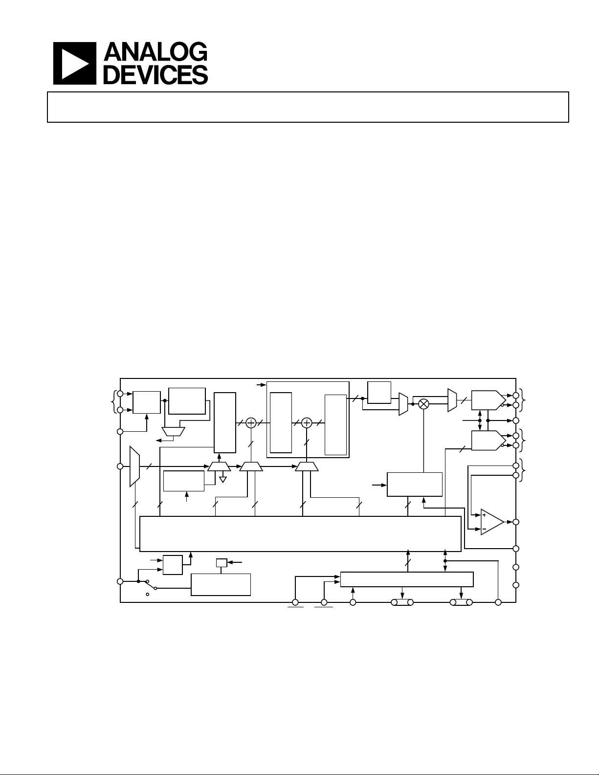
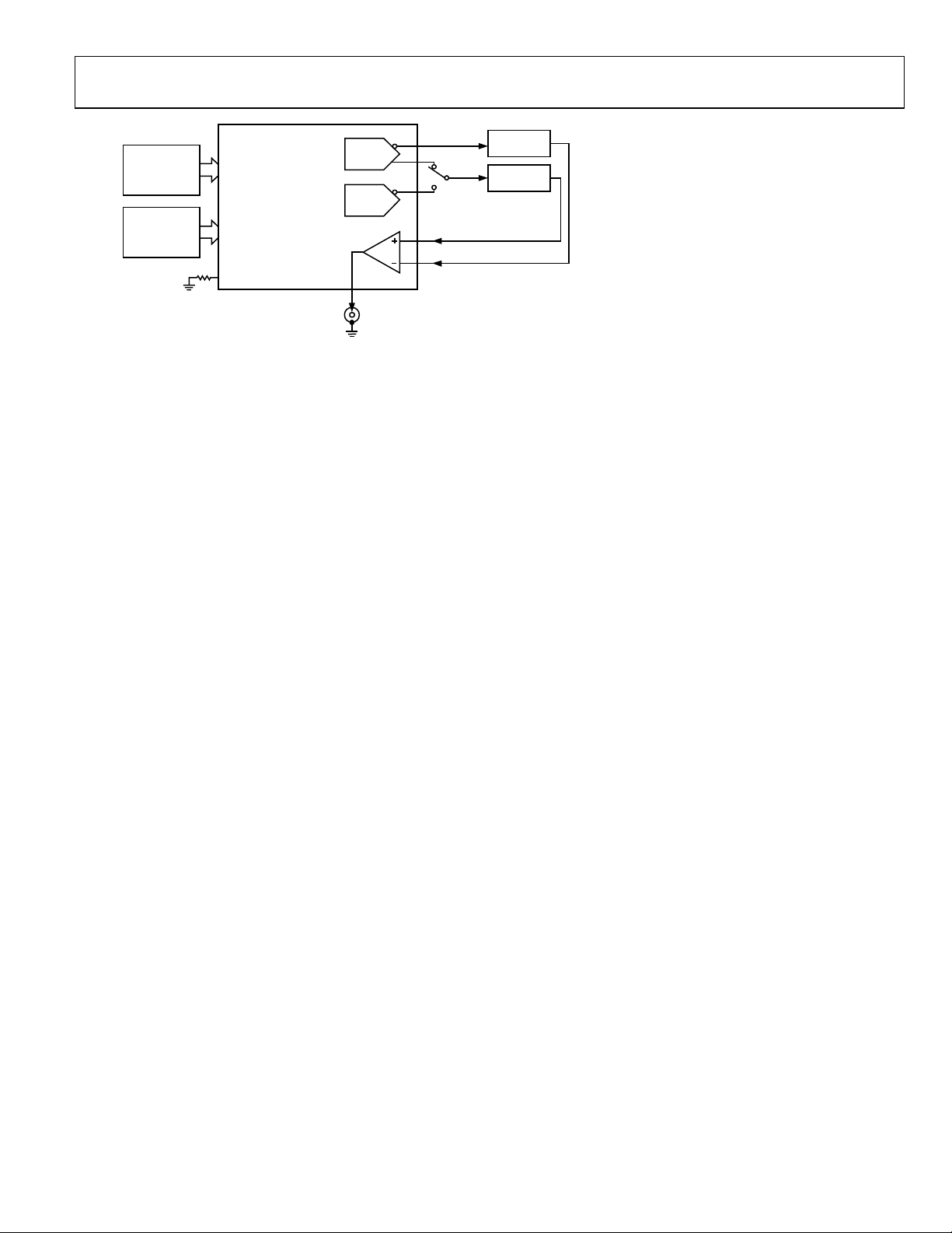
FUNCTIONAL BLOCK DIAGRAM
SYSTEM CLOCK
ACC 1
FREQUENCY
ACCUMULATOR
MUX
FREQUENCY
TUNING
WORD 1
INTERNAL
PROGRAMMABLE
UPDATE CLOCK
FREQUENCY
÷2
4848
48
MUX MUX
TUNING
WORD 2
PROGRAMMING REGISTERS
SYSTEM
CLOCK
<25 ps rms total jitter in clock generator mode
Automatic bidirectional frequency sweeping
SIN(x)/x correction
Simplified control interface
3.3 V single supply
Multiple power-down functions
Single-ended or differential input reference clock
Small 80-lead LQFP packaging
APPLICATIONS
Agile LO frequency synthesis
Programmable clock generator
FM chirp source for radar and scanning systems
Test and measurement equipment
Commercial and amateur RF exciter
DDS CORE
17
17
ACC 2
PHASE
ACCUMULATOR
FIRST 14-BIT
PHASE/OFFSET
WORD
READ WRITE SERIAL/
Figure 1.
14
AD9852
PHASE-TO-
Complete DDS
AD9852
10 MHz serial, 2-wire or 3-wire SPI® compatible, or
100 MHz parallel 8-bit programming
DIGITAL MULTIPLIERS
INV.
12
SINC
I
FILTER
AMPLITUDE
CONVERTER
Q
SYSTEM
CLOCK
14
SECOND 14-BIT
PHASE/OFFSET
WORD
PARALLEL
SELECT
MUX
PROGRAMMABLE
AMPLITUDE AND
RATE CONTROL
12
AM
MODULATION
BUS
I/O PORT BUFFERS
6-BIT ADDRESS
OR SERIAL
PROGRAMMING
LINES
MUX
SYSTEM
CLOCK
12-BIT DC
CONTROL
PARALLEL
12
12
8-BIT
LOAD
12-BIT
COSINE
DAC
12-BIT
CONTROL
DAC
COMPARATOR
MASTER
RESET
DAC R
CLOCK
OUT
OSK
GND
+V
ANALOG
OUT
SET
ANALOG
OUT
ANALOG
IN
S
00634-C-001
Rev. C
Information furnished by Analog Devices is believed to be accurate and reliable.
However, no responsibility is assumed by Analog Devices for its use, nor for any
infringements of patents or other rights of third parties that may result from its use.
Specifications subject to change without notice. No license is granted by implication
or otherwise under any patent or patent rights of Analog Devices. Trademarks and
registered trademarks are the property of their respective owners.
One Technology Way, P.O. Box 9106, Norwood, MA 02062-9106, U.S.A.
Tel: 781.329.4700
Fax: 781.326.8703 © 2004 Analog Devices, Inc. All rights reserved.
www.analog.com

AD9852
TABLE OF CONTENTS
General Description......................................................................... 3
Parallel I/O Operation ............................................................... 27
Overview........................................................................................ 3
Specifications..................................................................................... 4
Absolute Maximum Ratings............................................................ 7
Explanation of Test Levels........................................................... 7
Pin Configuration and Function Descriptions............................. 8
Typical Performance Characteristics ........................................... 10
Typical Applications ....................................................................... 14
Modes of Operation ....................................................................... 16
Using the AD9852........................................................................... 24
Internal and External Update Clock ........................................ 24
Output Shaped On/Off Keying (OSK) .................................... 24
Cosine DAC................................................................................. 25
Control DAC............................................................................... 25
Inverse SINC Function .............................................................. 26
REFCLK Multiplier.................................................................... 26
Serial Port I/O Operation.......................................................... 27
General Operation of the Serial Interface................................... 30
Instruction Byte .......................................................................... 30
Serial Interface Port Pin Descriptions..................................... 31
MSB/LSB Transfers .................................................................... 31
Control Register Descriptions.................................................. 32
Power Dissipation and Thermal Considerations....................... 34
Thermal Impedance................................................................... 34
Junction Temperature Considerations .................................... 34
Evaluation of Operating Conditions............................................ 36
Thermally Enhanced Package Mounting Guidelines............ 36
Evaluation Board ............................................................................ 38
Evaluation Board Instructions.................................................. 38
General Operating Instructions ............................................... 38
Using the Provided Software .................................................... 41
Programming the AD9852 ............................................................ 27
Master RESET ............................................................................. 27
REVISION HISTORY
4/04—Data Sheet Changed from Rev. B to Rev. C
Updated Format........................................................... Universal
Changes to Figure 1....................................................................1
Changes to General Description ..............................................3
Changes to Table 1......................................................................4
Changes to Footnote 2 ...............................................................6
Changes to Figure 2....................................................................8
Changes to Table 5....................................................................17
Changes to Equation in Ramped FSK (Mode 010)..............19
Changes to Evaluation Board Instructions ...........................39
Changes to General Operating Instructions Section...........39
Changes to Using the Provided Software Section ................42
Changes to Figure 65................................................................43
Changes to Figure 66................................................................44
Changes to Figure 72 and Figure 73.......................................48
Changes to Ordering Guide....................................................48
Outline Dimensions....................................................................... 48
Ordering Guide .......................................................................... 48
3/02—Changed from Rev. A to Rev. B:
Changes to General Description ..............................................1
Changes to Functional Block Diagram....................................1
Changes to Specifications.......................................................... 3
Changes to Absolute Maximum Ratings.................................5
Changes to Pin Function Descriptions....................................6
Changes to Figure 3....................................................................8
Deleted Two TPCs....................................................................11
Changes to Figure 18 and Figure 19.......................................11
Changes to BPDK Mode Section............................................21
Changes to Differential Refclk Enable Section..................... 24
Changes to Master Reset Section ...........................................24
Changes to Parallel I/O Operation Section...........................24
Changes to General Operation of the Serial
Interface Section .......................................................................27
Changes to Figure 50................................................................27
Changes to Figure 65................................................................36
Rev. C | Page 2 of 48

AD9852
GENERAL DESCRIPTION
The AD9852 digital synthesizer is a highly integrated device
that uses advanced DDS technology, coupled with an internal
high speed, high performance D/A converter to form a digitally
programmable agile synthesizer function. When referenced to
an accurate clock source, the AD9852 generates a highly stable,
frequency-phase-amplitude-programmable cosine output that
can be used as an agile LO in communications, radar, and many
other applications. The AD9852’s innovative high speed DDS
core provides 48-bit frequency resolution (1 MHz tuning
resolution with 300 MHz SYSCLK). Maintaining 17 bits assures
excellent SFDR.
The AD9852’s circuit architecture allows the generation of
output signals at frequencies up to 150 MHz, which can be
digitally tuned at a rate of up to 100 million new frequencies per
second. The (externally filtered) cosine wave output can be
converted to a square wave by the internal comparator for agile
clock generator applications. The device provides two 14-bit
phase registers and a single pin for BPSK operation. For high
order PSK operation, the I/O interface may be used for phase
changes. The 12-bit cosine DAC, coupled with the innovative
DDS architecture, provides excellent wideband and narrowband output SFDR. When configured with the comparator, the
12-bit control DAC facilitates static duty cycle control in the
high speed clock generator applications. The 12-bit digital
multiplier permits programmable amplitude modulation,
shaped on/off keying, and precise amplitude control of the
cosine DAC output. Chirp functionality is also included for
wide bandwidth frequency sweeping applications. The
AD9852’s programmable 4 × to 20 × REFCLK multiplier circuit
generates the 300 MHz system clock internally from a lower
frequency external reference clock. This saves the user the
expense and difficulty of implementing a 300 MHz system
clock source. Direct 300 MHz clocking is also accommodated
with either single-ended or differential inputs. Single pin
conventional FSK and the enhanced spectral qualities of
“ramped” FSK are supported. The AD9852 uses advanced
0.35 micron CMOS technology to provide this high level of
functionality on a single 3.3 V supply.
The AD9852 is available in a space-saving 80-lead LQFP
surface-mount package and a thermally enhanced 80-lead
LQFP package. The AD9852 is pin-for-pin compatible with the
AD9854 single-tone synthesizer. It is specified to operate over
the extended industrial temperature range of –40°C to +85°C.
OVERVIEW
The AD9852 digital synthesizer is a highly flexible device that
addresses a wide range of applications. The device consists of
an NCO with 48-bit phase accumulator, a programmable
reference clock multiplier, an inverse sinc filter, a digital
multiplier, two 12-bit/300 MHz DACs, a high speed analog
comparator, and interface logic. This highly integrated device
can be configured to serve as a synthesized LO agile clock
generator and FSK/BPSK modulator. The theory of operation of
the functional blocks of the device, and a technical description
of the signal flow through a DDS device is provided by Analog
Devices in “A Technical Tutorial on Digital Signal Synthesis.”
This tutorial is available in the DDS Technical Library of the
Analog Devices website at www.analog.com/dds. The tutorial
also provides basic applications information for a variety of
digital synthesis implementations.
Rev. C | Page 3 of 48

AD9852
SPECIFICATIONS
VS = 3.3 V ± 5%, R
external reference clock frequency = 20 MHz with REFCLK multiplier enabled at 10× for AD9852AST, unless otherwise noted.
Table 1.
Parameter
REF CLOCK INPUT CHARACTERISTICS1
Internal System Clock Frequency Range
REFCLK Multiplier Enabled Full VI 20 300 20 200 MHz
REFCLK Multiplier Disabled Full VI DC 300 DC 200 MHz
External REF Clock Frequency Range
REFCLK Multiplier Enabled Full VI 5 75 5 50 MHz
REFCLK Multiplier Disabled Full VI DC 300 DC 200 MHz
Duty Cycle 25°C IV 45 50 55 45 50 55 %
Input Capacitance 25°C IV 3 3 pF
Input Impedance 25°C IV 100 100 kΩ
Differential-Mode Common-Mode Voltage Range
Minimum Signal Amplitude2 25°C IV 400 400 mV p-p
Common-Mode Range 25°C IV 1.6 1.75 1.9 1.6 1.75 1.9 V
VIH (Single-Ended Mode) 25°C IV 2.3 2.3 V
VIL (Single-Ended Mode) 25°C IV 1 1 V
DAC STATIC OUTPUT CHARACTERISTICS
Output Update Speed Full I 300 200 MSPS
Resolution 25°C IV 12 12 Bits
Cosine and Control DAC Full-Scale Output Current 25°C IV 5 10 20 5 10 20 mA
Gain Error 25°C I
Output Offset 25°C I 2 2 µA
Differential Nonlinearity 25°C I 0.3 1.25 0.3 1.25 LSB
Integral Nonlinearity 25°C I 0.6 1.66 0.6 1.66 LSB
Output Impedance 25°C IV 100 100 kΩ
Voltage Compliance Range 25°C I
DAC DYNAMIC OUTPUT CHARACTERISTICS
DAC Wideband SFDR
1 MHz to 20 MHz A
20 MHz to 40 MHz A
40 MHz to 60 MHz A
60 MHz to 80 MHz A
80 MHz to 100 MHz A
100 MHz to 120 MHz A
DAC Narrow-Band SFDR
10 MHz A
10 MHz A
10 MHz A
41 MHz A
41 MHz A
41 MHz A
119 MHz A
119 MHz A
119 MHz A
OUT
OUT
OUT
OUT
OUT
OUT
OUT
OUT
OUT
= 3.9 kΩ; external reference clock frequency = 30 MHz with REFCLK multiplier enabled at 10× for AD9852ASQ;
SET
Temp
25°C V 58 58 dBc
OUT
25°C V 56 56 dBc
OUT
25°C V 52 52 dBc
OUT
25°C V 48 48 dBc
OUT
OUT
25°C V 48 dBc
OUT
25°C V 48 48 dBc
Test
Level
AD9852ASQ
Min Typ Max
+2.25
−6
+1.0
−0.5
AD9852AST
Min Typ Max Unit
+2.25 % FS
−6
+1.0 V
−0.5
(± 1 MHz) 25°C V 83 83 dBc
(± 250 kHz) 25°C V 83 83 dBc
(± 50 kHz) 25°C V 91 91 dBc
(± 1 MHz) 25°C V 82 82 dBc
(± 250 kHz) 25°C V 84 84 dBc
(± 50 kHz) 25°C V 89 89 dBc
(± 1 MHz) 25°C V 71 dBc
(± 250 kHz) 25°C V 77 dBc
(± 50 kHz) 25°C V 83 dBc
Rev. C | Page 4 of 48

AD9852
Parameter
Residual Phase Noise
(A
= 5 MHz, Ext. CLK = 30 MHz, REFCLK
OUT
Multiplier Engaged at 10×)
1 kHz Offset 25°C V 140 140 dBc/Hz
10 kHz Offset 25°C V 138 138 dBc/Hz
100 kHz Offset 25°C V 142 142 dBc/Hz
(A
= 5 MHz, Ext. CLK = 300 MHz, REFCLK
OUT
Multiplier Bypassed)
1 kHz Offset 25°C V 142 142 dBc/Hz
0 kHz Offset 25°C V 148 148 dBc/Hz
100 kHz Offset 25°C V 152 152 dBc/Hz
PIPELINE DELAYS3, 4, 5
DDS Core (Phase Accumulator and Phase-toAmp Converter)
Frequency Accumulator 25°C IV 26 26
Inverse Sinc Filter 25°C IV 16 16
Digital Multiplier 25°C IV 9 9
DAC 25°C IV 1 1
I/O Update Clock (INT Mode) 25°C IV 2 2
I/O Update Clock (EXT Mode) 25°C IV 3 3
MASTER RESET DURATION 25°C IV 10 10
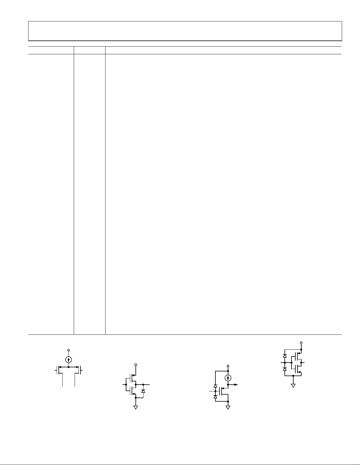
COMPARATOR INPUT CHARACTERISTICS
Input Capacitance 25°C V 3 3 pF
Input Resistance 25°C IV 500 500 kΩ
Input Current 25°C I ± 1 ± 5 ± 1 ± 5 µA
Hysteresis 25°C IV 10 20 10 20 mV p-p
COMPARATOR OUTPUT CHARACTERISTICS
Logic 1 Voltage, High Z Load Full VI 3.1 3.1 V
Logic 0 Voltage, High Z Load Full VI 0.16 0.16 V
Output Power, 50 Ω Load, 120 MHz Toggle Rate 25°C I 9 11 9 11 dBm
Propagation Delay 25°C IV 3 3 ns
Output Duty Cycle Error6 25°C I
Rise/Fall Time, 5 pF Load 25°C V 2 2 ns
Toggle Rate, High Z Load 25°C IV 300 350 300 350 MHz
Toggle Rate, 50 Ω Load 25°C IV 375 400 375 400 MHz
Output Cycle-to-Cycle Jitter7 25°C IV 4.0 4.0 ps rms
COMPARATOR NARROWBAND SFDR
8
10 MHz (± 1 MHz) 25°C V 84 84 dBc
10 MHz (± 250 MHz) 25°C V 84 84 dBc
10 MHz (± 50 kHz) 25°C V 92 92 dBc
41 MHz (± 1 MHz) 25°C V 76 76 dBc
41 MHz (± 250 kHz) 25°C V 82 82 dBc
41 MHz (± 50 kHz) 25°C V 89 89 dBc
119 MHz (± 1 MHz) 25°C V 73 dBc
119 MHz (± 250 kHz) 25°C V 73 dBc
119 MHz (± 50 kHz) 25°C V 83 dBc
Temp
Test
Level
AD9852ASQ
Min Typ Max
AD9852AST
Min Typ Max Unit
25°C IV 33 33
SysClk
cycles
SysClk
cycles
SysClk
cycles
SysClk
cycles
SysClk
cycles
SysClk
cycles
SysClk
cycles
SysClk
cycles
−10
± 1 +10
± 1 +10 %
−10
Rev. C | Page 5 of 48

AD9852
Parameter
Temp
Test
Level
AD9852ASQ
Min Typ Max
AD9852AST
Min Typ Max
CLOCK GENERATOR OUTPUT JITTER8
5 MHz A
40 MHz A
100 MHz A
25°C V 23 23 ps rms
OUT
25°C V 12 12 ps rms
OUT
25°C V 7 7 ps rms
OUT
PARALLEL I/O TIMING CHARACTERISTICS
T
(Address Setup Time to WR Signal Active)
ASU
T
(Address Hold Time to WR Signal Inactive)
ADHW
T
(Data Setup Time to WR Signal Inactive)
DSU
T
(Data Hold Time to WR Signal Inactive)
DHD
T
(WR Signal Minimum Low Time)
WRLOW
T
(WR Signal Minimum High Time)
WRHIGH
Full IV 8.0 7.5 8.0 7.5 ns
Full IV 0 0 ns
Full IV 3.0 1.6 3.0 1.6 ns
Full IV 0 0 ns
Full IV 2.5 1.8 2.5 1.8 ns
Full IV 7 7 ns
TWR (Minimum WRITE Time) Full IV 10.5 10.5 ns
T
(Address to Data Valid Time) Full V 15 15 15 15 ns
ADV
T
(Address Hold Time to RD Signal Inactive)
ADHR
T
(RD Low-to-Output Valid)
RDLOV
T
(RD High-to-Data Three-State)
RDHOZ
Full IV 5 5 ns
Full IV 15 15 ns
Full IV 10 10 ns
SERIAL I/O TIMING CHARACTERISTICS
T
(CS Setup Time)
PRE
T
(Period of Serial Data Clock) Full IV 100 100 ns
SCLK
T
(Serial Data Setup Time) Full IV 30 30 ns
DSU
T
(Serial Data Clock Pulse Width High) Full IV 40 40 Ns
SCLKPWH
T
(Serial Data Clock Pulse Width Low) Full IV 40 40 Ns
SCLKPWL
T
(Serial Data Hold Time) Full IV 0 0 Ns
DHLD
Full IV 30 30 ns
TDV (Data Valid Time) Full V 30 30 ns
CMOS LOGIC INPUTS 9
Logic 1 Voltage 25°C I 2.2 2.2 V
Logic 0 Voltage 25°C I 0.8 0.8 V
Logic ” Current 25°C IV ± 5 ± 12 µA
Logic 0 Current 25°C IV ± 5 ± 12 µA
Input Capacitance 25°C V 3 3 pF
POWER SUPPLY
10
+VS Current11 25°C I 815 922 585 660 mA
+VS Current12 25°C I 640 725 465 520 mA
+VS Current13 25°C I 585 660 425 475 mA
P
11 25°C I 2.70 3.20 1.93 2.39 W
DISS
P
12 25°C I 2.12 2.52 1.53 1.81 W
DISS
P
13 25°C I 1.93 2.29 1.40 1.65 W
DISS
P
Power-Down Mode 25°C I 1 50 1 50 mW
DISS
1
The reference clock inputs are configured to accept a 1 V p-p (typical) dc offset square or sine waves centered at one-half the applied VDD or a 3 V TTL-level pulse input.
2
An internal 400 mV p-p differential voltage swing equates to 200 mV p-p applied to both REFCLK input pins.
3
Pipeline delays of each individual block are fixed; however, if the eight top MSBs of a tuning word are all zeros, the delay appears appear longer. This is due to
insufficient phase accumulation per a system clock period to produce enough LSB amplitude to the D/A converter.
4
If a feature such as inverse sinc, which has 16 pipeline delays, can be bypassed, the total delay is reduced by that amount.
5
The I/O Update CLK transfers data from the I/O port buffers to the programming registers. This transfer takes system clocks to perform.
6
Change in duty cycle from 1 MHz to 100 MHz with 1 V p-p sine wave input and 0.5 V threshold.
7
Represents comparator’s inherent cycle-to-cycle jitter contribution. Input signal is a 1 V, 40 MHz square wave. Measurement device Wavecrest DTS – 2075.
8
Comparator input originates from analog output section via external 7-pole elliptic LPF. Single-ended input, 0.5 V p-p. Comparator output terminated in 50 Ω.
9
Avoid overdriving digital inputs. (Refer to equivalent circuits in .) Figure 3
10
Simultaneous operation at the maximum ambient temperature of 85°C and the maximum internal clock frequency of 200 MHz for the 80-lead LQFP, or 300 MHz for
the thermally enhanced 80-lead LQFP may cause the maximum die junction temperature of 150°C to be exceeded. Refer to the Power Dissipation and Thermal
Considerations section for derating and thermal management information.
11
All functions engaged.
12
All functions except inverse sinc engaged.
13
All functions except inverse sinc and digital multipliers engaged.
Unit
Rev. C | Page 6 of 48

AD9852
ABSOLUTE MAXIMUM RATINGS
Table 2.
Parameter Rating
Maximum Junction Temperature 150°C
V
S
Digital Inputs
Digital Output Current 5 mA
Storage Temperature
Operating Temperature
Lead Temperature (Soldering, 10 s) 300°C
Maximum Clock Frequency (ASQ) 300 MHz
Maximum Clock Frequency (AST) 200 MHz
θJA (ASQ) 16°C/W
θJC (ASQ) 2°C/W
θJA (AST) 38°C/W
4 V
−0.7 V to +V
−65°C to +150°C
−40°C to +85°C
S
Stresses above those listed under Absolute Maximum Ratings
may cause permanent damage to the device. This is a stress
rating only and functional operation of the device at these or
any other condition s above those indicated in the operational
section of this specification is not implied. Exposure to absolute
maximum rating conditions for extended periods may affect
device reliability.
EXPLANATION OF TEST LEVELS
Tes t Le v el
1. 100% production tested.
2. Sample tested only.
3. Parameter is guaranteed by design and characterization
testing.
4. Parameter is a typical value only.
5. Devices are 100% production tested at 25°C and
guaranteed by design and characterization testing for
industrial operating temperature range.
ESD CAUTION
ESD (electrostatic discharge) sensitive device. Electrostatic charges as high as 4000 V readily accumulate on
the human body and test equipment and can discharge without detection. Although this product features
proprietary ESD protection circuitry, permanent damage may occur on devices subjected to high energy
electrostatic discharges. Therefore, proper ESD precautions are recommended to avoid performance
degradation or loss of functionality.
Rev. C | Page 7 of 48
AD9852
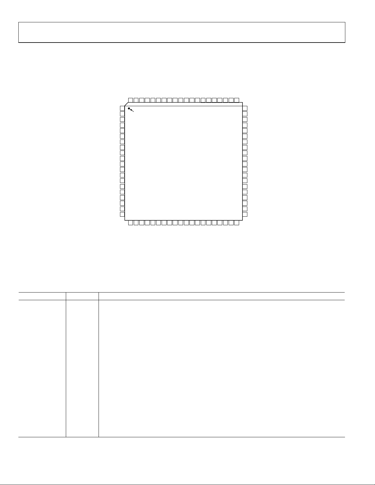
PIN CONFIGURATION AND FUNCTION DESCRIPTIONS
AGND
S/P SELECT
REFCLK
REFCLKB
34 35 36 37 38 39 40
AVDD
AVDD
AGND
AGND
DVDD
DVDD
DGND
DGND
NC
A2/IO RESET
A1/SDO
A0/SDIO
I/O UD CLK
DVDD
DVDD
DGND
DGND
DGND
DVDD
DVDD
DVDD
DGND
DGND
80 79 78 77 76 71 70 69 6875 74 73 72
1
D7
D6
D5
D4
D3
D2
D1
D0
A5
A4
A3
PIN 1
2
INDICATOR
3
4
5
6
7
8
9
10
11
12
13
14
15
16
17
18
19
20
21 22 23 24 25 26 27 28 29 30 31 32 33
RDB/CSB
WRB/SCLK
DVDD
DVDD
DGND
AD9852
TOP VIEW
(Not to Scale)
DGND
DGND
MASTER RESET
OSK
AGND
AVDD
NC
VOUT
DIFF CLK ENABLENCAGND
64 63 62 6167 66 65
AVDD
AVDD
PLL FILTER
AGND
AGND
60
59
58
57
56
55
54
53
52
51
50
49
48
47
46
45
44
43
42
41
AVDD
AGND
NC
NC
DAC R
DACBP
AVDD
AGND
IOUT2
IOUT2B
AVDD
IOUT1B
IOUT1
AGND
AGND
AGND
AVDD
VINN
VINP
AGND
SET
NC = NO CONNECT
RGK/BPSK/HOLD
00634-C-002
Figure 2. Pin Configuration
Table 3.
Pin Number Mnemonic Function
1–8 D7–D0 8-bit bidirectional parallel programming data Inputs. Used only in parallel programming mode.
9, 10, 23, 24, 25,
73, 74, 79, 80
11, 12, 26, 27, 28,
DVDD
Connections for the digital circuitry supply voltage. Nominally 3.3 V more positive than AGND and
DGND.
DGND Connections for digital circuitry ground return. Same potential as AGND.
72, 75, 76, 77, 78
13, 35, 57, 58, 63 NC No internal connection
14–19 A5–A0
6-bit parallel address inputs for program registers. Used only in parallel programming mode. A0, A1, and
A2 have a second function when the serial programming mode is selected. See following descriptions.
17
A2/IO
RESET
Allows an IO RESET of the serial communications bus that is unresponsive due to improper
programming protocol. Resetting the serial bus in this manner does not affect previous programming,
nor does it invoke the “default” programming values seen in Table 7. Active HIGH.
18 A1/SDO Unidirectional serial data output for use in 3-wire serial communication mode.
19 A0/SDIO Bidirectional serial data input/output for use in 2-wire serial communication mode.
20 I/O UD CLK
Bidirectional I/O update CLK. Direction is selected in control register. If selected as an input, a rising edge
transfers the contents of the I/O port buffers to the programming registers. If I/O UD is selected as an
output (default), an output pulse (low to high) of eight system clock cycle duration indicates that an
internal frequency update has occurred.
21 WRB/SCLK
Write parallel data to I/O port buffers. Shared function with SCLK. Serial clock signal associated with the
serial programming bus. Data is registered on the rising edge. This pin is shared with WRB when the
parallel mode is selected. Mode dependent on Pin 70 (S/P Select).
Rev. C | Page 8 of 48
AD9852
Pin Number Mnemonic Function
22 RDB/CSB
29
FSK/BPSK/
HOLD
30
OUTPUT
SHAPED
KEYING
31, 32, 37, 38, 44,
AVDD
50, 54, 60, 65
33, 34, 39, 40, 41,
AGND Connections for analog circuitry ground return. Same potential as DGND.
45, 46, 47, 53, 59,
62, 66, 67
36 VOUT
42 VINP Voltage input positive. The internal high speed comparator’s noninverting input.
43 VINN Voltage input negative. The internal high speed comparator’s inverting input.
48 IOUT1 Unipolar current output of the cosine DAC. (Refer to Figure 3.)
49 IOUT1B Complementary unipolar current output of the cosine DAC.
51 IOUT2B Complementary unipolar current output of the control DAC.
52 IOUT2 Unipolar current output of the control DAC.
55 DACBP
56 DAC R
61 PLL FILTER
64
DIFF CLK
ENABLE
68 REFCLKB
69 REFCLK
70 S/P SELECT Selects between serial programming mode (logic low) and parallel programming mode (logic high).
71
MASTER
RESET
AVDD
Read parallel data from programming registers. Shared function with CSB. Chip select signal associated
with the serial programming bus. Active low. This pin is shared with RDB when the parallel mode is
selected.
Multifunction pin according to the mode of operation selected in the programming control register. If in
the FSK mode, logic low selects F1, logic high selects F2. If in the BPSK mode, logic low selects Phase 1,
logic high selects Phase 2. In chirp mode, logic high engages the HOLD function causing the frequency
accumulator to halt at its current location. To resume or commence chirp, logic low is asserted.
Must first be selected in the programming control register to function. A logic high causes the cosine
DAC outputs to ramp up from zero-scale to full-scale amplitude at a preprogrammed rate. Logic low
causes the full-scale output to ramp down to zero scale at the preprogrammed rate.
Connections for the analog circuitry supply voltage. Nominally 3.3 V more positive than AGND and
DGND.
Internal high speed comparator’s noninverted output pin. Designed to drive 10 dBm to 50 Ω loads as
well as standard CMOS logic levels.
Common bypass capacitor connection for both DACs. A 0.01 µF chip cap from this pin to AVDD improves
harmonic distortion and SFDR slightly. No connect is permissible (slight SFDR degradation).
Common connection for both DACs to set the full-scale output current. R
SET
= 39.9/ I
SET
. Normal R
OUT
range is from 8 kΩ (5 mA) to 2 kΩ (20 mA).
This pin provides the connection for the external zero compensation network of the REFCLK multiplier’s
PLL loop filter. The zero compensation network consists of a 1.3 kΩ resistor in series with a 0.01 µF
capacitor. The other side of the network should be connected to AVDD as close as possible to Pin 60. For
optimum phase noise performance, the REFCLK multiplier can be bypassed by setting the “Bypass PLL”
bit in control register 1E.
Differential REFCLK ENABLE. A high level of this pin enables the differential clock inputs, REFCLK and
REFCLKB (Pins 69 and 68, respectively).
The COMPLEMENTARY (180 Degrees Out-of-Phase) differential clock signal. User should tie this pin high
or low when single-ended clock mode is selected. Same signal levels as REF CLK.
Single-ended (CMOS logic levels required) reference clock input or one of two differential clock signals.
In differential reference clock mode, both inputs can be CMOS logic levels or have greater than
400 mV p-p square or sine waves centered about 1.6 V dc.
Initializes the serial/parallel programming bus to prepare for user programming; sets programming
registers to a “do-nothing” state defined by the default values seen in Table 7. Active on logic high.
Asserting MASTER RESET is essential for proper operation upon power-up.
DVDD
SET
AVDD
I
OUTIOUTB
MUST TERMINATE OUTPUTS
FOR CURRENT FLOW. DO
NOT EXCEED THE OUTPUT
VOLTAGE COMPLIANCE RATING.
A. DAC Outputs B. Comparator Output C. Comparator Input D. Digital Inputs
COMPARATOR
OUT
Figure 3. Equivalent Input and Output Circuits
Rev. C | Page 9 of 48
VINP/
VINN
AVDD
DIGITAL
IN
AVOID OVERDRIVING
DIGITAL INPUTS. FORWARD
BIASING ESD DIODES MAY
COUPLE DIGITAL NOISE
ONTO POWER PINS.
00634-C-003
AD9852
–
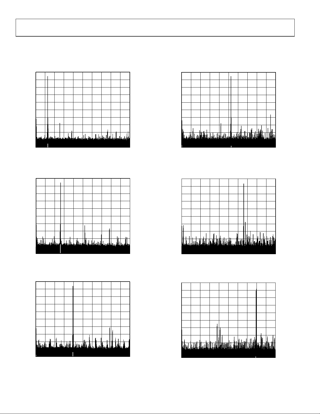
TYPICAL PERFORMANCE CHARACTERISTICS
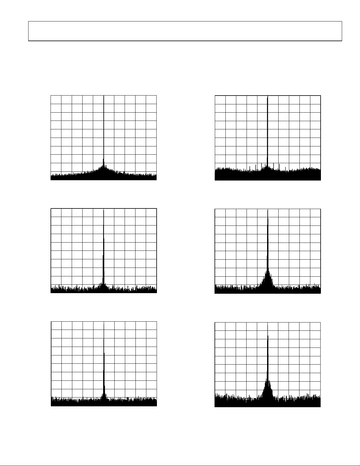
Figure 4 to Figure 9 indicate the wideband harmonic distortion performance of the AD9852 from 19.1 MHz to 119.1 MHz fundamental
output, reference clock = 30 MHz, REFCLK multiplier = 10. Each graph plotted from 0 MHz to 150 MHz (Nyquist).
–10
–20
–30
–40
–50
–60
–70
–80
–90
–100
0
START 0Hz
15MHz/ STOP 150MHz
00634-C-004
–10
–20
–30
–40
–50
–60
–70
–80
–90
–100
0
START 0Hz
15MHz/ STOP 150MHz
00634-C-007
–10
–20
–30
–40
–50
–60
–70
–80
–90
–100
–10
–20
–30
–40
–50
–60
–70
–80
–90
–100
0
START 0Hz
0
START 0Hz
Figure 4. Wideband SFDR, 19.1 MHz
15MHz/ STOP 150MHz
Figure 5. Wideband SFDR, 39.1 MHz
15MHz/ STOP 150MHz
Figure 6. Wideband SFDR, 59.1 MHz
00634-C-005
00634-C-006
–10
–20
–30
–40
–50
–60
–70
–80
–90
100
–10
–20
–30
–40
–50
–60
–70
–80
–90
–100
0
START 0Hz
0
START 0Hz
Figure 7. Wideband SFDR, 79.1 MHz
15MHz/ STOP 150MHz
Figure 8. Wideband SFDR, 99.1 MHz
15MHz/ STOP 150MHz
Figure 9. Wideband SFDR, 119.1 MHz
00634-C-008
00634-C-009
Rev. C | Page 10 of 48
AD9852
–
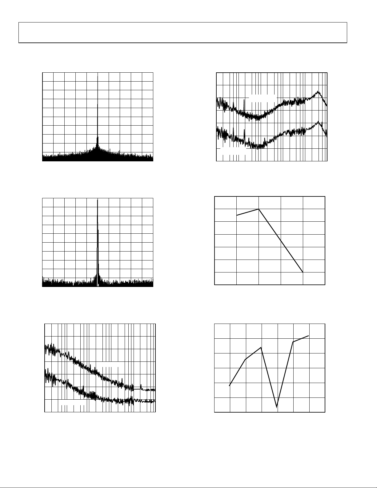
Figure 10 to Figure 13 show the trade-off in elevated noise floor, increased phase noise, and discrete spurious energy when the internal
REFCLK multiplier circuit is engaged. Plots with wide (1 MHz) and narrow (50 kHz) spans are shown.
Compare the noise floor of Figure 11 and Figure 13 to Figure 14 and Figure 15. The improvement seen in Figure 11 and Figure 13 is a
direct result of sampling the fundamental at a higher rate. Sampling at a higher rate spreads the quantization noise of the DAC over a
wider bandwidth, which effectively lowers the noise floor.
0
–10
–20
–30
–40
–50
–60
–70
–80
–90
–100
CENTER 39.1MHz
100kHz/ SPAN 1MHz
00634-C-010
Figure 10. Narrow-band SFDR, 39.1 MHz, 1 MHz BW, 300 MHz REFCLK with
REFCLK Multiply Bypassed
0
–10
–20
–30
–40
–50
–60
–70
–80
–90
100
CENTER 39.1MHz
5kHz/ SPAN 50kHz
00634-C-011
Figure 11. Narrow-band SFDR, 39.1 MHz, 50 kHz BW, 300 MHz REFCLK with
REFCLK Multiplier Bypassed
0
–10
–20
–30
–40
–50
–60
–70
–80
–90
–100
CENTER 39.1MHz
5kHz/ SPAN 50kHz
00634-C-012
Figure 12. Narrow-band SFDR, 39.1 MHz, 50 kHz BW, 100 MHz, REFCLK with
REFCLK Multiplier Bypassed
0
–10
–20
–30
–40
–50
–60
–70
–80
–90
–100
CENTER 39.1MHz
100kHz/ SPAN 1MHz
00634-C-013
Figure 13. Narrow-band SFDR, 39.1 MHz, 1 MHz BW, 30 MHz REFCLK with
REFCLK Multiply =10x
0
–10
–20
–30
–40
–50
–60
–70
–80
–90
–100
CENTER 39.1MHz
5kHz/ SPAN 50kHz
00634-C-014
Figure 14. Narrow-band SFDR, 39.1 MHz, 50 kHz BW, 30 MHz REFCLK with
REFCLK Multiplier = 10x
0
–10
–20
–30
–40
–50
–60
–70
–80
–90
–100
CENTER 39.1MHz
5kHz/ SPAN 50kHz
00634-C-015
Figure 15. Narrow-band SFDR, 39.1 MHz, 50 kHz BW, 10 MHz REFCLK with
REFCLK Multiplier = 10x
Rev. C | Page 11 of 48
AD9852
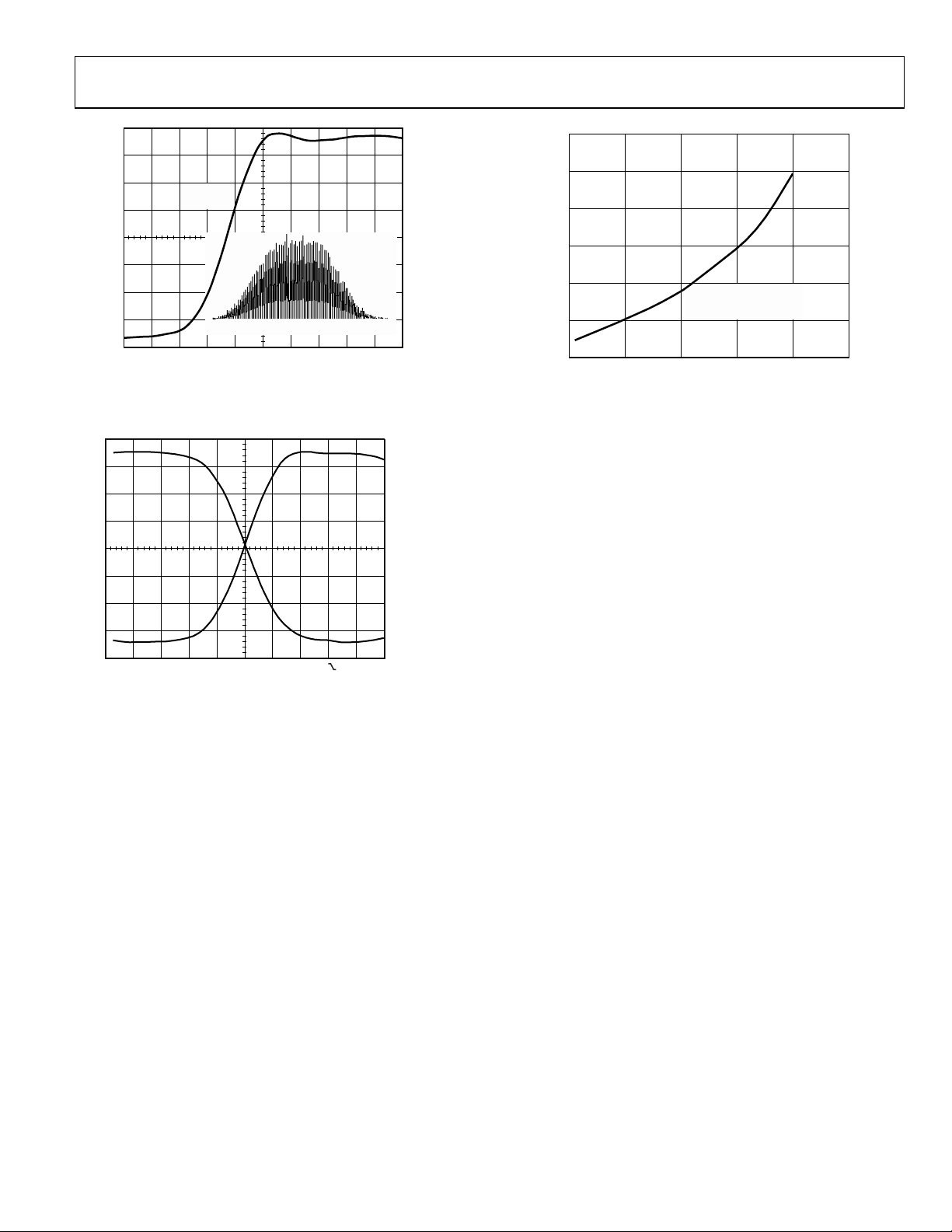
Figure 17 shows the narrow-band performance of the AD9852 when operating with a 20 MHz reference clock and the REFCLK multiplier
enabled at 10×vs. a 200 MHz reference clock with REFCLK multiplier bypassed.
0
–10
–20
–30
–40
–50
–60
–70
–80
–90
–100
CENTER 112.469MHz
50kHz/ SPAN 500kHz
00634-C-016
–90
–100
–110
–120
–130
–140
PHASE NOISE (dBc/Hz)
–150
A
= 5MHz
OUT
–160
10 1M100 100k10k1k
A
= 80MHz
OUT
FREQUENCY (Hz)
00634-C-019
Figure 16. A Slight Change in Tuning Word Yields Dramatically Better Results.
112.469 MHz with All Spurs Shifted Out-of-Band. RECLK is 300 MHz.
0
–10
–20
–30
–40
–50
–60
–70
–80
–90
–100
CENTER 39.1MHz
5kHz/ SPAN 50kHz
00634-C-017
Figure 17. Narrow-band SFDR, 39.1 MHz, 50 kHz BW, 200 MHz REFCLK with
REFCLK Multiplier Bypassed
–100
–110
–120
–130
–140
–150
PHASE NOISE (dBc/Hz)
–160
–170
10 1M100 100k10k1k
A
OUT
= 5MHz
A
= 80MHz
OUT
FREQUENCY (Hz)
00634-C-018
Figure 19. Residual Phase Noise, 30 MHz REFCLK with
REFCLK Multiplier = 10x
55
54
53
52
51
SFDR (dBc)
50
49
48
0
5 10152025
DAC CURRENT (mA)
Figure 20. SFDR vs. DAC Current, 59.1 A
Multiplier Bypassed
620
615
610
605
600
SUPPLY CURRENT (mA)
595
590
0
20 40 60 80 100 120 140
FREQUENCY (MHz)
, 300 MHz REFCLK with REFCLK
OUT
00634-C-020
00634-C-021
Figure 18. Residual Phase Noise, 300 MHz REFCLK with REFCLK Multiplier
Bypassed
Rev. C | Page 12 of 48
Figure 21. Supply Current vs. Output Frequency; Variation Is Minimal as a
Percentage and Heavily Dependent on Tuning Word
AD9852
1200
1000
RISE TIME
1.04ns
800
[10.6ps RMS]
–33ps 0ps +33ps
500ps/DIV 232mV/DIV 50Ω INPUT
Figure 22. Typical Comparator Output Jitter, 40 MHz A
with REFCLK Multiplier Bypassed
CH1 500mVΩ M 500ps CH1
Figure 23. Comparator Rise/Fall Times
JITTER
, 300 MHz REFCLK
OUT
REF1 RISE
1.174ns
C1 FALL
1.286ns
980mV
00634-C-022
00634-C-023
600
400
AMPLITUDE (mV p-p)
200
0
0
100 200 300 400 500
MINIMUM COMPARATOR
INPUT DRIVE
V
= 0.5V
CM
FREQUENCY (MHz)
00634-C-024
Figure 24. Comparator Toggle Voltage Requirement
Rev. C | Page 13 of 48
AD9852
TYPICAL APPLICATIONS
RF/IF
INPUT
BASEBAND
REFCLK
Rx
RF IN
VCA
ADC CLOCK FREQUENCY
Figure 26. Chip Rate Generator in Spread Spectrum Application
BAND-PASS
FC + F
IMAGE
FILTER
O
AD9852
AD9852
SPECTRUM
FUNDAMENTAL
FC– F
IMAGE
I
OUT
50Ω
O
F
CLK
Figure 27. Using an Aliased Image to Generate a High Frequency
AMPLIFIER
50Ω
FINAL OUTPUT
SPECTRUM
FC + F
AD9852
LOW-PASS
FILTER
COS
Figure 25. Synthesized LO Application for the AD9852
I/Q MIXER
AND
LOW-PASS
FILTER
LOCKED TO Tx CHIP/
SYMBOL/PN RATE
REFERENCE
CLOCK
O
IMAGE
BAND-PASS
FILTER
I
Q
DUAL
8-/10-BIT
ADC
AD9852
CLOCK
GENERATOR
00634-C-027
8
8
ADC ENCODE
48
CHIP/SYMBOL/PN
RATE DATA
REFERENCE
CLOCK
DIGITAL
DEMODULATOR
AD9852
DDS
TUNING
WORD
Figure 29. Agile High Frequency Synt hesizer
00634-C-025
AGC
FILTER
Rx BASEBAND
DIGITAL
DATA OUT
PHASE
COMPARATOR
DIVIDE-BY-N
00634-C-026
LOOP
FILTER
RF FREQUENCY
OUT
VCO
00634-C-029
REFERENCE
CLOCK
LOOP
FILTER
REF CLK IN
“DIVIDE-BY-N” FUNCTION
(WHERE N = 2
VCO
PROGRAMMABLE
48
/TUNING WORD)
FILTER
DAC OUT
PHASE
COMPARATOR
AD9852
DDS
TUNING
WORD
Figure 28. Programmable Fractional Divide-by-N Synthesizer
RF FREQUENCY
OUT
REFERENCE
00634-C-028
Rev. C | Page 14 of 48
DIFFERENTIAL
TRANSFORMER-COUPLED
OUTPUT
I
CLOCK
AD9852
DDS
OUT
I
OUT
50Ω
1:1 TRANSFORMER
I.E., MINI-CIRCUITS T1-1T
Figure 30. Differential Output Connection for Reduction
of Common-Mode Signals
FILTER
50Ω
00634-C-030
AD9852
µPROCESSOR/
CONTROLLER
FPGA, ETC.
REFERENCE
CLOCK
AD9852
8-BIT PARALLEL OR
SERIAL PROGRAMMING
DATA AND CONTROL
SIGNALS
300MHz MAX DIRECT
MODE OR 15 TO 75MHZ
MAX IN THE 4× – 20× CLOCK
MULTIPLIER MODE
2kΩ
R
SET
COSINE
DAC
CONTROL
DAC
1
2
LOW-PASS
FILTER
LOW-PASS
FILTER
NOTES
= APPROX 20mA MAX WHEN R
I
OUT
SWITCH POSTION 1 PROVIDES COMPLEMENTARY
SINUSOIDAL SIGNALS TO THE COMPARATOR TO
PRODUCE A FIXED 50% DUTY CYCLE FROM THE
COMPARATOR.
SWITCH POSTION 2 PROVIDES A USER-PROGRAMMABLE
DC THRESHOLD VOLTAGE TO ALLOW SETTING OF THE
COMPARATOR DUTY CYCLE.
SET
= 2kΩ
CMOS LOGIC “CLOCK” OUT
00634-C-031
Figure 31. Frequency Agile Clock Generator Applications for the AD9852
Rev. C | Page 15 of 48

AD9852
K
MODES OF OPERATION
There are five programmable modes of operation of the
AD9852. Selecting a mode requires that three bits in the
Control Register (parallel address 1F hex) be programmed
as follows in Table 4.
Table 4. Mode Selection Table
Mode 2 Mode 1 Mode 0 Result
0 0 0 SINGLE-TONE
0 0 1 FSK
0 1 0 RAMPED FSK
0 1 1 CHIRP
1 0 0 BPSK
In each mode, engaging certain functions may not be
permitted.
Figure 32 graphically shows the transition from the default
condition (0 Hz) to a user-defined output frequency (F1).
As with all Analog Devices DDSs, the value of the frequency
tuning word is determined using the following equation:
FTW = (Desired Output Frequency × 2N)/SYSCLK
where N is the phase accumulator resolution (48 bits in this
instance), frequency is expressed in Hertz, and the FTW,
Frequency Tuning Word, is a decimal number.
Once a decimal number has been calculated, it must be rounded
to an integer and then converted to binary format—a series of
48 binary weighted 1s or 0s. The fundamental sine wave DAC
output frequency range is from dc to 1/2 SYSCLK.
Table 5 shows a listing of some important functions and their
availability for each mode.
Single-Tone (Mode 000)
This is the default mode when master reset is asserted. It may
also be accessed by being user-programmed into the control
register. The Phase Accumulator, responsible for generating an
output frequency, is presented with a 48-bit value from
Frequency Tuning Word 1 registers whose default values are
zero. Default values from the remaining applicable registers
further define the single-tone output signal qualities.
The default values after a master reset configure the device with
an output signal of 0 Hz, 0 phase. Upon power-up and reset,
the output from both DACs is a dc value equal to the midscale
output current. This is the default mode amplitude setting of
zero. Refer to the digital multiplier section for further explanation of the output amplitude control. It is necessary to program
all or some of the 28 program registers to realize a user-defined
output signal.
FREQUENCY
F1
0
MODE
000 (DEFAULT)
Changes in frequency are phase-continuous, thus the first
sampled phase value of the new frequency is referenced in time
from the last sampled phase value of the previous frequency.
The 14-bit phase register adjusts the cosine DAC’s output phase.
The single-tone mode allows the user to control the following
signal qualities:
• Output frequency to 48-bit accuracy
• Output amplitude to 12-bit accuracy
– Fixed, user-defined, amplitude control
– Variable, programmable amplitude control
– Automatic, programmable, single pin controlled,
shaped on/off keying
• Output phase to 14-bit accuracy
Furthermore, all of these qualities can be changed or modulated
via the 8-bit parallel programming port at a 100 MHz parallelbyte rate, or at a 10 MHz serial rate. Incorporating this attribute
permits FM, AM, PM, FSK, PSK, and ASK operation i n the
single-tone mode.
000 (SINGLE TONE)
0
MASTER RESET
I/O UPDATE CL
Figure 32. Default State to User-Defined Output Transition
F1TW1
00634-C-032
Rev. C | Page 16 of 48

AD9852
Table 5. Function Availability vs. Mode of Operation
Function Single-Tone Mode FSK Mode Ramped FSK Mode CHIRP Mode BPSK Mode
Phase Adjust 1
Phase Adjust 2
Single Pin FSK/BPSK or HOLD
Single Pin Shaped Keying
Phase Offset or Modulation
Amplitude Control or Modulation
Inverse SINC Filter
Frequency Tuning Word 1
Frequency Tuning Word 2
Automatic Frequency Sweep
Unramped FSK (Mode 001)
When selected, the output frequency of the DDS is a function
of the values loaded into Frequency Tuning Word Registers 1
and 2 and the logic level of Pin 29 (FSK/BPSK/HOLD). A logic
low on Pin 29 chooses F1 (frequency tuning word 1, parallel
address 4–9 hex) and a logic high chooses F2 (frequency tuning
word 2, parallel register address A–F hex). Changes in frequency
are phase-continuous and are internally coincident with the
FSK data pin (29); however, there is deterministic pipeline delay
between the FSK data signal and the DAC output (see Table 1).
The unramped FSK mode, Figure 33, is representative of
traditional FSK, Radio Teletype (RTTY) or Teletype (TTY)
transmission of digital data. FSK is a very reliable means of
digital communication; however, it makes inefficient use of the
bandwidth in the RF spectrum. Ramped FSK in Figure 34 is a
method of conserving the bandwidth.
√ √ √ √ √
√ √ √ √
√ √ √ √ √
√ √ √ √
√ √ √ √ √
√ √ √ √ √
√ √ √ √ √
√ √
√ √
Ramped FSK (Mode 010)
In this method of FSK, changes from F1 to F2 are not instantaneous but are accomplished in a frequency sweep or “ramped”
fashion. The ramped notation implies that the sweep is linear.
While linear sweeping or frequency ramping is easily and
automatically accomplished, it is only one of many possibilities.
Other frequency transition schemes may be implemented by
changing the ramp rate and ramp step size on-the-fly, in
piecewise fashion.
Frequency ramping, whether linear or nonlinear, necessitates
that many intermediate frequencies between F1 and F2 are
output in addition to the primary F1 and F2 frequencies.
Figure 34 and Figure 35 graphically depict the frequency
versus time characteristics of a linear ramped FSK signal.
NOTE: In ramped FSK mode, the delta frequency (DFW) is
required to be programmed as a positive twos complement
value. Another requirement is that the lowest frequency (F1)
be programmed in the Frequency Tuning Word 1 register.
√
F2
FREQUENCY
F1
0
MODE
TW1
TW2
I/O UPDATE CLK
FSK DATA (PIN 29)
000 (DEFAULT)
0
0
Figure 33. Traditional FSK Mode
001 (FSK NO RAMP)
F1
F2
00634-C-033
Rev. C | Page 17 of 48

AD9852
FREQUENCY
MODE
F2
F1
0
000 (DEFAULT)
010 (RAMPED FSK)
TW1
TW2
DFW
I/O UPDATE CLK
FSK DATA (PIN 29)
FREQUENCY
MODE
TW1
TW2
I/O UPDATE
CLOCK
FSK DATA
0
0
F2
F1
0
000 (DEFAULT)
0
0
F1
F2
REQUIRES A POSITIVE TWOS COMPLEMENT VALUE
RAMP RATE
Figure 34. Ramped FSK Mode
010 (RAMPED FSK)
F1
F2
Figure 35. Ramped FSK Mode
00634-C-034
00634-C-035
The purpose of ramped FSK is to provide better bandwidth
containment than traditional FSK by replacing the instantaneous frequency changes with more gradual, user-defined
frequency changes. The dwell time at F1 and F2 can be equal
to or much greater than the time spent at each intermediate
frequency. The user controls the dwell time at F1 and F2, the
number of intermediate frequencies and time spent at each
frequency. Unlike unramped FSK, ramped FSK requires the
lowest frequency to be loaded into F1 registers and the highest
frequency into F2 registers.
Rev. C | Page 18 of 48
Several registers must be programmed to instruct the DDS
regarding the resolution of intermediate frequency steps
(48 bits) and the time spent at each step (20 bits). Furthermore,
the CLR ACC1 bit in the control register should be toggled
(low-high-low) prior to operation to assure that the frequency
accumulator is starting from an “all zeros” output condition. For
piecewise, nonlinear frequency transitions, it is necessary to
reprogram the registers while the frequency transition is in
progress to affect the desired response.

AD9852
T
T
Parallel register addresses 1A–1C hex comprise the 20-bit ramp
rate clock registers. This is a countdown counter that outputs a
single pulse whenever the count reaches zero. The counter is
activated any time a logic level change occurs on FSK input
Pin 29. This counter is run at the system clock rate, 300 MHz
maximum. The time period between each output pulse is
(N+1)(System Clock Period × 2)
where N is the 20-bit ramp rate clock value programmed by the
user. The allowable range of N is from 1 to (2
20
– 1). The output
of this counter clocks the 48-bit frequency accumulator shown
in Figure 35. The Ramp Rate Clock determines the amount of
time spent at each intermediate frequency between F1 and F2.
The counter stops automatically when the destination
frequency is achieved. The dwell time spent at F1 and F2 is
determined by the duration that the FSK input, Pin 29, is held
high or low after the destination frequency has been reached.
Parallel register addresses 10–15 hex comprise the 48-bit, twos
complement, delta frequency word registers. This 48-bit word is
accumulated (added to the accumulator’s output) every time it
receives a clock pulse from the ramp rate counter. The output of
this accumulator is then added to or subtracted from the F1 or
F2 frequency word, which is then fed to the input of the 48-bit
phase accumulator that forms the numerical phase steps for the
sine and cosine wave outputs. In this fashion, the output
frequency is ramped up and down in frequency, according to
the logic state of Pin 29. The rate at which this happens is a
function of the 20-bit ramp rate clock. Once the destination
frequency is achieved, the ramp rate clock is stopped, which
halts the frequency accumulation process.
Generally speaking, the delta frequency word is a much smaller
value compared to that of the F1 or F2 tuning word. For
example, if F1 and F2 are 1 kHz apart at 13 MHz, the delta
frequency word might be only 25 Hz.
Figure 40 shows that premature toggling causes the ramp to
immediately reverse itself and proceed at the same rate and
resolution back to originating frequency.
The control register contains a triangle bit at parallel register
address 1F hex. Setting this bit high in Mode 010 causes an
automatic ramp-up and ramp-down between F1 and F2 to
occur without having to toggle Pin 29 as shown in Figure 37. In
fact, the logic state of Pin 29 has no effect once the triangle bit is
set high. This function uses the ramp-rate clock time period
and the delta-frequency-word step size to form a continuously
sweeping linear ramp from F1 to F2 and back to F1 with equal
dwell times at every frequency. Use this function to automatically sweep between any two frequencies from dc to Nyquist.
In the ramped FSK mode, with the triangle bit set high, an
automatic frequency sweep begins at either F1 or F2, according
to the logic level on Pin 29 (FSK input pin) when the triangle
bit’s rising edge occurs as shown in Figure 38. If the FSK data bit
had been high instead of low, F2 rather than F1 would have
been chosen as the start frequency.
PHASE
ACCUMULATOR
TUNING
WORD 1
ADDER
FSK (PIN 29)
FREQUENCY
TUNING
WORD 2
010 (RAMPED FSK)
F1
F2
010 (RAMPED FSK)
SYSTEM
CLOCK
F1
F2
INSTANTANEOUS
PHASE OUT
FREQUENCY
ACCUMULATOR
48-BIT DELTA
FREQUENCY
WORD (TWOS
COMPLEMENT)
FREQUENCY
20-BIT
RAMP RATE
CLOCK
Figure 36. Block Diagram of Ramped FSK Function
F2
FREQUENCY
F1
0
MODE
TW1
TW2
FSK DATA
TRIANGLE
BIT
I/O UPDATE
CLOCK
Figure 37. Effect of Triangle Bit in Ramped FSK Mode
F2
FREQUENCY
F1
0
MODE
000 (DEFAULT)
TW1
TW2
FSK DATA
RIANGLE BI
0
0
Figure 38. Automatic Linear Ramping Using the Triangle Bit
00634-C-036
00634-C-037
00634-C-038
Rev. C | Page 19 of 48

AD9852
E
E
Additional flexibility in the ramped FSK mode is provided in
the ability to respond to changes in the 48-bit delta frequency
word and/or the 20-bit ramp-rate counter on-the-fly during the
ramping from F1 to F2 or vice versa. To create these nonlinear
frequency changes, it is necessary to combine several linear
ramps, in a piecewise fashion, with differing slopes. This is done
by programming and executing a linear ramp at some rate or
“slope” and then altering the slope (by changing the ramp rate
clock or delta frequency word or both). Changes in slope are
made as often as needed to form the desired nonlinear
frequency sweep response before the destination frequency has
been reached. These piecewise changes can be precisely timed
using the 32-bit internal update clock (see the Internal and
External Update Clock section).
Nonlinear ramped FSK has the appearance of a chirp function
that is graphically illustrated in Figure 41. The major difference
between a ramped FSK function and a chirp function is that
FSK is limited to operation between F1 and F2. Chirp operation
has no F2 limit frequency.
The AD9852 permits precise, internally generated linear
or externally programmed nonlinear, pulsed or continuous
FM over the complete frequency range, duration, frequency
resolution, and sweep direction(s). All of these are userprogrammable. A block diagram of the FM chirp components
is shown in Figure 39.
F2
FREQUENCY
F1
0
MODE
I/O UPDAT
CLOCK
FSK DATA
TW1
TW2
000 (DEFAULT)
0
0
Figure 39. FM Chirp Components
010 (RAMPED FSK)
F1
F2
00634-C-039
Two additional control bits are available in the ramped FSK
mode that allow even more options. CLR ACC1, register address
1F hex, if set high, clears the 48-bit frequency accumulator
(ACC1) output with a retriggerable one-shot pulse of one
system clock duration. If the CLR ACC1 bit is left high, a oneshot pulse is delivered on the rising edge of every Update Clock.
The effect is to interrupt the current ramp, reset the frequency
back to the start point, F1 or F2, and then continue to ramp up
(or down) at the previous rate. This occurs even when a static
F1 or F2 destination frequency has been achieved.
Next, CLR ACC2 control bit (register address 1F hex) is
available to clear both the frequency accumulator (ACC1) and
the phase accumulator (ACC2). When this bit is set high, the
output of the phase accumulator results in 0 Hz output from the
DDS. As long as this bit is set high, the frequency and phase
accumulators are cleared, resulting in 0 Hz output. To return to
previous DDS operation, CLR ACC2 must be set to logic low.
Chirp (Mode 011)
This mode is also known as pulsed FM. Most chirp systems use
a linear FM sweep pattern, but the AD9852 supports nonlinear
patterns as well. In radar applications, use of chirp or pulsed FM
allows operators to significantly reduce the output power
needed to achieve the same result as a single frequency radar
system would produce. Figure 41 represents a very low
resolution nonlinear chirp meant to demonstrate the different
slopes that are created by varying the time steps (ramp rate) and
frequency steps (delta frequency word).
MODE
DFW
RAMP RAT
I/O UPDATE
CLOCK
FREQUENCY
TW1
ACCUMULATOR
FREQUENCY
ACCUMULATOR
48-BIT DELTA
FREQUENCY
WORD (TWOS
COMPLEMENT)
HOLD
20-BIT
RAMP RATE
CLOCK
CLR ACC1
ADDER
FREQUENCY
TUNING
WORD 1
Figure 40. Effect of Premature Ramped FSK Data
F1
0
000 (DEFAULT)
0
010 (RAMPED FSK)
Figure 41. Example of a Nonlinear Chirp
PHASE
SYSTEM
CLOCK
F1
OUT
CLR ACC2
00634-C-040
00634-C-041
Rev. C | Page 20 of 48

AD9852
Basic FM Chirp Programming Steps
1. Program a start frequency into Frequency Tuning Word 1
(parallel register addresses 4–9 hex) hereafter called FTW1.
2. Program the frequency step resolution into the 48-bit, twos
complement, delta frequency word (parallel register
addresses 10–15 hex).
3. Program the rate of change (time at each frequency) into
the 20-bit ramp rate clock (parallel register addresses
1A–1C hex).
When programming is complete, an I/O update pulse at Pin 20
engages the program commands.
The necessity for a twos complement delta frequency word is to
define the direction in which the FM chirp moves. If the 48-bit
delta frequency word is negative (MSB is high), then the
incremental frequency changes are in a negative direction from
FTW1. If the 48-bit word is positive (MSB is low), then the
incremental frequency changes are in a positive direction.
It is important to note that FTW1 is only a starting point for
FM chirp. There is no built-in restraint requiring a return to
FTW1. Once the FM chirp has begun, it is free to move (under
program control) within the Nyquist bandwidth (dc to 1/2
system clock). Instant return to FTW1 is easily achieved,
though, as described next.
Two control bits are available in the FM Chirp mode that allow
the return to the beginning frequency, FTW1, or to 0 Hz. First,
when the CLR ACC1 bit (register address 1F hex) is set high,
the 48-bit frequency accumulator (ACC1) output is cleared with
a retriggerable one-shot pulse of one system clock duration.
The 48-bit Delta Frequency Word input to the accumulator is
unaffected by CLR ACC1 bit. If the CLR ACC1bit is held high,
a one-shot pulse is delivered to the frequency accumulator
(ACC1) on every rising edge of the I/O Update clock. The effect
is to interrupt the current chirp, reset the frequency back to
FTW1, and continue the chirp at the previously programmed
rate and direction. Figure 42 illustrates clearing the frequency
accumulator output in chirp mode
Shown in the diagram is the I/O update clock, which is either
user-supplied or internally generated. A discussion of I/O
update is presented elsewhere in this data sheet.
Next, CLR ACC2 control bit (register address 1F hex) is
available to clear both the frequency accumulator (ACC1) and
the phase accumulator (ACC2). When this bit is set high, the
output of the phase accumulator results in 0 Hz output from the
DDS. As long as this bit is set high, the frequency and phase
accumulators are cleared, resulting in 0 Hz output. To return to
previous DDS operation, CLR ACC2 must be set to logic low.
This bit is useful in generating pulsed FM.
FREQUENCY
F1
0
000 (DEFAULT)
MODE
FTW1
DFW
RAMP
RATE
I/O UPDATE
CLOCK
CLR ACC1
0
Figure 42. Effect of CLR ACC1 in FM Chirp Mode
011 (CHIRP)
F1
DELTA FREQUENCY WORD
RAMP RATE
00634-C-042
Rev. C | Page 21 of 48

AD9852
Figure 43 graphically illustrates the effect of CLR ACC2 bit
upon the DDS output frequency. Note that reprogramming the
registers while the CLR ACC2 bit is high allows a new FTW1
frequency and slope to be loaded.
Another function available only in the chirp mode is the
HOLD pin, Pin 29. This function stops the clock signal to the
ramp rate counter, thereby halting any further clocking pulses
to the frequency accumulator, ACC1. The effect is to halt the
FREQUENCY
F1
0
chirp at the frequency existing just before HOLD was pulled
high. When the HOLD pin is returned low, the clocks are
resumed and chirp continues. During a hold condition, the user
may change the programming registers; however, the ramp rate
counter must resume operation at its previous rate until a count
of zero is obtained before a new ramp rate count can be loaded.
Figure 44 illustrates the effect of the hold function on the DDS
output frequency.
MODE
TW1
DPW
RAMP RATE
CLR ACC2
I/O UPDATE
CLOCK
000 (DEFAULT)
0
011 (CHIRP)
00634-C-043
Figure 43. Effect of CLR ACC2 in FM Chirp Mode
FREQUENCY
F1
0
MODE
TW1
000 (DEFAULT)
0
011 (CHIRP)
F1
DFW
RAMP RATE
HOLD
I/O UPDATE
CLOCK
DELTA FREQUENCY WORD
RAMP RATE
Figure 44. Illustration of HOLD Function
Rev. C | Page 22 of 48
00634-C-044

AD9852
The 32-bit automatic I/O update counter may be used to
construct complex chirp or ramped FSK sequences. Because
this internal counter is synchronized with the AD9852 system
clock, it allows precisely timed program changes to be invoked.
This way the user is only required to reprogram the desired
registers before the automatic I/O update clock is generated.
In chirp mode, the destination frequency is not directly specified. If the user fails to control the chirp, the DDS naturally
confines itself to the frequency range between dc and Nyquist.
Unless terminated by the user, the chirp continues until power
is removed.
When the chirp destination frequency is reached there are
several possible outcomes:
1. Stop at the destination frequency using the HOLD pin, or
by loading all zeros into the delta frequency word registers
of the frequency accumulator (ACC1).
2. Use the HOLD pin function to stop the chirp, then ramp-
down the output amplitude using the digital multiplier
stages and the shaped-keying pin, Pin 30, or via program
register control (addresses 21–24 hex).
3. Abruptly terminate the transmission with bit CLR ACC2.
4. Continue chirp by reversing direction and returning to the
previous, or another, destination frequency in a linear or
user-directed manner. If this involves going down in
frequency, a negative 48-bit delta frequency word (the MSB
is set to 1) must be loaded into registers 10–15 hex. Any
decreasing frequency step of the delta frequency word
requires the MSB to be set to logic high.
5. Continue chirp by immediately returning to the beginning
frequency (F1) in a saw tooth fashion and repeat the
previous chirp process. This is where CLR ACC1 control
bit is used. An automatic, repeating chirp can be set up
using the 32-bit update clock to issue CLR ACC1
command at precise time intervals. Adjusting the timing
intervals or changing the delta frequency word changes the
chirp range. It is incumbent upon the user to balance the
chirp duration and frequency resolution to achieve the
proper frequency range.
BPSK (Mode 100)
Binary, biphase or bipolar phase shift keying is a means to
rapidly select between two preprogrammed 14-bit output phase
offsets. The logic state of Pin 29, the BPSK pin, controls the
selection of Phase Adjust Register 1 or 2. When low, Pin 29
selects Phase Adjust Register 1; when high, Phase Adjust
Register 2 is selected. Figure 45 illustrates phase changes made
to four cycles of an output carrier.
Basic BPSK Programming Steps
1. Program a carrier frequency into frequency tuning word 1.
2. Program appropriate 14-bit phase words in Phase Adjust
Registers 1 and 2.
3. Attach the BPSK data source to Pin 29.
4. Activate the I/O update clock when ready.
Note: If higher order PSK modulation is desired, the user can
select single-tone mode and program phase adjust Register 1
using the serial or high speed parallel programming bus.
MODE
FTW1
PHASE ADJUST 1
PHASE ADJUST 2
BPSK DATA
I/O UPDATE
CLOCK
360
PHASE
0
000 (DEFAULT)
0
Figure 45. BPSK Mode
Rev. C | Page 23 of 48
100 (BPSK)
F1
270 DEGREES
90 DEGREES
00634-C-045

AD9852
USING THE AD9852
INTERNAL AND EXTERNAL UPDATE CLOCK
The update clock function is comprised of a bidirectional I/O
pin, Pin 20, and a programmable 32-bit down-counter. In order
for programming changes to be transferred from the I/O buffer
registers to the active core of the DDS, a clock signal (low to
high edge) must be externally supplied to Pin 20 or internally
generated by the 32-bit update clock.
When the user provides an external update clock, it is internally
synchronized with the system clock to prevent partial transfer
of program register information due to violation of data setup
or hold times. This mode gives the user complete control of
when updated program information becomes effective. The
default mode for update clock is internal (Int Update Clk
control register bit is logic high). To switch to external update
clock mode, the Int Update Clk register bit must be set to logic
low. The internal update mode generates automatic, periodic
update pulses with the time period set by the user.
Otherwise, if the OSK EN bit is set low, the digital multiplier
responsible for amplitude control is bypassed and the cosine
DAC output is set to full-scale amplitude. In addition to setting
the OSK EN bit, a second control bit, OSK INT (also at address
20 hex), must be set to logic high. Logic high selects the linear
internal control of the output ramp-up or ramp-down function.
A logic low in the OSK INT bit switches control of the digital
multiplier to user programmable 12-bit register allowing users
to dynamically shape the amplitude transition in practically any
fashion. The 12-bit register, labeled Output Shape Key, is located
at addresses 21–22 hex in Table 7. The maximum output
amplitude is a function of the R
resistor and is not
SET
programmable when OSK INT is enabled.
ABRUPT ON/OFF KEYING
ZERO
SCALE
FULL
SCALE
An internally generated update clock can be established by
programming the 32-bit update clock registers (address
16–19 hex) and setting the Int Update Clk (address 1F hex)
control register bit to logic high. The update clock downcounter function operates at 1/2 the rate of the system clock
(150 MHz maximum) and counts down from a 32-bit binary
value (programmed by the user). When the count reaches 0, an
automatic I/O update of the DDS output or functions is
generated. The update clock is internally and externally routed
on Pin 20 to allow users to synchronize programming of update
information with the update clock rate. The time period
between update pulses is given as
(N + 1) × System Clock Period
where N is the 32-bit value programmed by the user. Allowable
32
range of N is from 1 to (2
− 1). The internally generated
update pulse output on Pin 20 has a fixed high time of eight
system clock cycles.
Programming the update clock register for values less than
five causes the I/O UD pin to remain high. The update clock
functionality still works; however, the user cannot use the signal
as an indication that data is transferring. This is an effect of the
minimum high pulse time when I/O UD is an output.
OUTPUT SHAPED ON/OFF KEYING (OSK)
This feature allows the user to control the amplitude vs. time
slope of the cosine DAC output signal. This function is used in
burst transmissions of digital data to reduce the adverse spectral
impact of short, abrupt bursts of data. Users must first enable
the digital multiplier by setting the OSK EN bit (control register
address 20 hex) to logic high in the control register.
ZERO
SCALE
SHAPED ON/OFF KEYING
Figure 46. Shaped On/Off Keying
FULL
SCALE
The transition time from zero scale to full scale must also be
programmed. The transition time is a function of two fixed
elements and one variable. The variable element is the
programmable 8-bit ramp rate counter. This is a down-counter
that is clocked at the system clock rate (300 MHz max) and
generates one pulse whenever the counter reaches zero. This
pulse is routed to a 12-bit counter that increments with each
pulse received. The outputs of the 12-bit counter are connected
to the 12-bit digital multiplier. When the digital multiplier has a
value of all zeros at its inputs, the input signal is multiplied by
zero, producing zero scale. When the multiplier has a value of
all ones, the input signal is multiplied by a value of 4095/4096,
producing nearly full scale. There are 4094 remaining fractional
multiplier values that produce output amplitudes scaled
according to their binary values.
The two fixed elements of the transition time are the period of
the system clock (which drives the ramp rate counter) and the
number of amplitude steps (4096). To give an example, assume
that the system clock of the AD9852 is 100 MHz (10 ns period).
If the ramp rate counter is programmed for a minimum count
of three, it takes two system clock periods (one rising edge loads
the count-down value, the next edge decrements the counter
from three to two). If the count-down value is less than three,
the ramp rate counter stalls and, therefore, produces a constant
scaling value to the digital multiplier. This stall condition may
have application to the user.
00634-C-046
Rev. C | Page 24 of 48

AD9852
(BYPASS MULTIPLIER)
12-BIT DIGITAL
MULTIPLIER
OSK EN = 0
OSK EN = 1
COSINE
DAC
DDS DIGITAL
OUTPUT
DIGITAL
SIGNAL IN
OSK EN = 0
12 12
OSK EN = 1
USER-PROGRAMMABLE
12-BIT MULTIPLIER
“OUTPUT SHAPE
KEY MULT” REGISTER
12
Figure 47. Block Diagram of the Digital Multiplier Section Responsible for Shaped Keying Function
The relationship of the 8-bit count-down value to the time
period between output pulses is given as
(N + 1) × System Clock Period
where N is the 8-bit count-down value. It takes 4096 of these
pulses to advance the 12-bit up-counter from zero scale to full
scale. Therefore, the minimum shaped keying ramp time for a
100 MHz system clock is 4096 × 4 × 10 ns = approximately
164 µs. The maximum ramp time is
4096 × 256 × 10 ns = approximately 10.5 ms
Finally, by changing the logic state of Pin 30, shaped keying
automatically performs the programmed output envelope
functions when OSK INT is high. A logic high on Pin 30 causes
the outputs to linearly ramp up to full-scale amplitude and hold
until the logic level is changed to low, causing the outputs to
ramp down to zero scale.
COSINE DAC
The cosine output of the DDS drives the cosine DAC
(300 MSPS maximum). Its maximum output amplitude is set
by the DAC R
with a full-scale maximum output of 20 mA; however, a
nominal 10 mA output current provides best spurious-free
dynamic range (SFDR) performance. The value of R
39.93/I
OUT
specification limits the maximum voltage developed at the
outputs to –0.5 V to +1 V. Voltages developed beyond this
limitation cause excessive DAC distortion and possibly
permanent damage. The user must choose a proper load
impedance to limit the output voltage swing to the compliance
limits. Both DAC outputs should be terminated equally for best
SFDR, especially at higher output frequencies where harmonic
distortion errors are more prominent.
The cosine DAC is preceded by an inverse SIN(x)/x filter (also
called an inverse sinc filter) that precompensates for DAC
output amplitude variations over frequency to achieve flat
amplitude response from dc to Nyquist. This DAC can be
resistor at Pin 56. This is a current-out DAC
SET
, where I
is in amps. DAC output compliance
OUT
SET
=
12
OSK INT = 0
OSK INT = 1
12
12-BIT
UP/DOWN
COUNTER
8-BIT RAMP
1
RATE
COUNTER
SHAPED ON/OFF
KEYING PIN
SYSTEM
CLOCK
00634-C-047
powered down by setting the DAC PD bit high (address 1D of
control register) when not needed. Cosine DAC outputs are
designated as IOUT1 and IOUT1B, Pins 48 and 49, respectively.
Control DAC outputs are designated as IOUT2 and IOUT2B,
Pins 52 and 51, respectively.
CONTROL DAC
The control DAC output can provide dc control levels to
external circuitry, generate ac signals, or enable duty cycle
control of the on-board comparator. The input to the control
DAC is configured to accept twos complement data, supplied by
the user. Data is channeled through the serial or parallel interface to the 12-bit control DAC register (address 26 and 27 hex)
at a maximum 100 MHz data rate. This DAC is clocked at the
system clock, 300 MSPS (maximum), and has the same
maximum output current capability as that of the cosine DAC.
The single R
current for both DACs. The control DAC can be separately
powered down for power conservation when not needed by
setting the control DAC power-down bit high (address 1D hex).
Control DAC outputs are designated as IOUT2 and IOUT2B
(Pins 52 and 51, respectively).
4.0
3.5
3.0
2.5
2.0
1.5
1.0
0.5
dB
–0.5
–1.0
–1.5
–2.0
–2.5
–3.0
–3.5
–4.0
resistor on the AD9852 sets the full-scale output
SET
ISF
0
0 0.1
FREQUENCY NORMALIZED TO SAMPLE RATE
0.2 0.3 0.4 0.5
SYSTEM
SINC
Figure 48. Inverse SINC Filter Response
00634-C-048
Rev. C | Page 25 of 48

AD9852
INVERSE SINC FUNCTION
This filter precompensates input data to the cosine DAC for
the SIN(x)/x roll-off characteristic inherent in the DAC’s
output spectrum. This allows wide bandwidth signals (such
as QPSK) to be output from the DAC without appreciable
amplitude variations as a function of frequency. The inverse
SINC function may be bypassed to significantly reduce power
consumption, especially at higher clock speeds.
Inverse SINC is engaged by default and is bypassed by bringing
the Bypass Inv SINC bit high in control register 20 (hex), as
shown in Table 7.
REFCLK MULTIPLIER
This is a programmable PLL-based reference clock multiplier
that allows the user to select an integer clock multiplying value
over the range of 4× to 20×. Use of this function allows users
to input as little as 15 MHz at the REFCLK input to produce
a 300 MHz internal system clock. Five bits in control register
1E hex set the multiplier value, as described in Table 6.
Differential REFCLK Enable
A high level on this pin enables the differential clock inputs,
REFCLK and REFCLKB (Pins 69 and 68, respectively). The
minimum differential signal amplitude required is 400 mV p-p
at the REFCLK input pins. The center point or common-mode
range of the differential signal can range from 1.6 V to 1.9 V.
When Pin 64 (DIFF CLK ENABLE) is tied low, REFCLK
(Pin 69) is the only active clock input. This is referred to as
single-ended mode. In this mode, Pin 68 (REFCLKB) should
be tied low or high.
High Speed Comparator
The comparator is optimized for high speed, has a >300 MHz
toggle rate, low jitter, sensitive input, built-in hysteresis. It also
has an output level of 1 V p-p minimum into 50 Ω or CMOS
logic levels into high impedance loads. The comparator can be
separately powered down to conserve power. This comparator
is used in clock generator applications to square up the filtered
sine wave generated by the DDS.
The REFCLK multiplier function can be bypassed to allow
direct clocking of the AD9852 from an external clock source.
The system clock for the AD9852 is either the output of the
REFCLK multiplier (if it is engaged) or the REFCLK inputs.
REFCLK may be either a single-ended or differential input by
setting Pin 64, DIFF CLK ENABLE, low or high, respectively.
PLL Range Bit
The PLL range bit selects the frequency range of the REFCLK
multiplier PLL. For operation from 200 MHz to 300 MHz,
(internal system clock rate) the PLL range bit should be set to
Logic 1. For operation below 200 MHz, set the PLL range bit to
Logic 0. The PLL range bit adjusts the PLL loop parameters for
optimized phase noise performance within each range.
Pin 61, PLL Filter
This pin provides the connection for the external zero compensation network of the PLL loop filter. The zero compensation
network consists of a 1.3 kΩ resistor in series with a 0.01 µF
capacitor. The other side of the network should be connected
as close as possible to Pin 60, AVDD. For optimum phase noise
performance, the clock multiplier can be bypassed by setting
the Bypass PLL bit in control register address 1E.
Power-Down
Several individual stages may be powered down to reduce
power consumption via the programming registers while still
maintaining functionality of desired stages. These stages are
identified in the Register Layout table, address 1D hex. Powerdown is achieved by setting the specified bits to logic high. A
logic low indicates that the stages are powered up.
Furthermore, and perhaps most significantly, the Inverse Sinc
filters and the digital multiplier stages, can be bypassed to
achieve significant power reduction through programming of
the control registers in address 20 hex. Again, logic high causes
the stage to be bypassed. Of particular importance is the inverse
sinc filter as this stage consumes a significant amount of power.
A full power-down occurs when all four PD bits in control
register 1D hex are set to logic high. This reduces power
consumption to approximately 10 mW (3 mA).
Rev. C | Page 26 of 48

AD9852
PROGRAMMING THE AD9852
The AD9852 Register Layout, shown in Table 7, contains the
information that programs a chip for the desired functionality.
While many applications require very little programming to
configure the AD9852, some make use of all 12 accessible
register banks. The AD9852 supports an 8-bit parallel I/O
operation or an SPI compatible serial I/O operation. All
accessible registers can be written and read back in either I/O
operating mode.
S/P SELECT, Pin 70, is used to configure the I/O mode. Systems
that use the parallel I/O mode must connect the S/P SELECT
pin to V
the S/P SELECT pin to GND.
Regardless of mode, the I/O port data is written to a buffer
memory that does not affect operation of the part until the
contents of the buffer memory are transferred to the register
banks. This transfer of information occurs synchronously to
the system clock and occurs in one of two ways:
1. The transfer is internally controlled at a rate programmable
2. The transfer is externally controlled by the user. I/O
. Systems that operate in the serial I/O mode must tie
DD
by the user.
operations can occur in the absence of REFCLK but the
data cannot be moved from the buffer memory to the
register bank without REFCLK. (See the Internal and
External Update Clock section for details.)
MASTER RESET
Logic high active must be held high for a minimum of 10
system clock cycles. This causes the communications bus to be
initialized and loads default values listed in Table 7.
PARALLEL I/O OPERATION
With the S/P SELECT pin tied high, the parallel I/O mode is
active. The I/O port is compatible with industry-standard DSPs
and microcontrollers. Six address bits, eight bidirectional data
bits, and separate write/read control inputs make up the I/O
port pins.
Parallel I/O operation allows write access to each byte of any
register in a single I/O operation up to 1/10.5 ns. Read back
capability for each register is included to ease designing with
the AD9852.
Reads are not guaranteed at 100 MHz as they are intended for
software debugging only.
Parallel I/O operation timing diagrams are shown in Figure 49
and Figure 50.
Table 6. REFCLK Multiplier Control Register Values
Ref Mult
Multiplier
Value
4 0 0 1 0 0
5 0 0 1 0 1
6 0 0 1 1 0
7 0 0 1 1 1
8 0 1 0 0 0
9 0 1 0 0 1
10 0 1 0 1 0
11 0 1 0 1 1
12 0 1 1 0 0
13 0 1 1 0 1
14 0 1 1 1 0
15 0 1 1 1 1
16 1 0 0 0 0
17 1 0 0 0 1
18 1 0 0 1 0
19 1 0 0 1 1
20 1 0 1 0 0
Bit 4 Bit 3 Bit 2 Bit 1 Bit 0
SERIAL PORT I/O OPERATION
With the S/P SELECT pin tied low, the serial I/O mode is active.
The AD9852 serial port is a flexible, synchronous, serial
communications port allowing easy interface to many industrystandard microcontrollers and microprocessors. The serial I/O
is compatible with most synchronous transfer formats,
including both the Motorola 6905/11 SPI and Intel® 8051 SSR
protocols. The interface allows read/write access to all 12
registers that configure the AD9852 and can be configured as a
single pin I/O (SDIO) or two unidirectional pins for in/out
(SDIO/SDO). Data transfers are supported in most significant
bit (MSB) first format or least significant bit (LSB) first format
at up to 10 MHz.
When configured for serial I/O operation, most pins from the
AD9852 parallel port are inactive; some are used for the serial
I/O. Table 8 describes pin requirements for serial I/O.
Note: When operating in the serial I/O mode, it is best to use
the external I/O update CLK mode to avoid an I/O update CLK
during a serial communication cycle. Such an occurrence could
cause incorrect programming due to partial data transfer. Thus,
the user would want to write between I/O update CLKs. To
exit the default internal update mode, program the device for
external update operation at power-up, before starting the
REFCLK signal, but after a master reset. Starting the REFCLK
causes this information to transfer to the register bank, putting
the device in external update mode.
Rev. C | Page 27 of 48

AD9852
Table 7. Register Layout
Shaded sections comprise the control register.
Parallel
Address
Hex
00
01
02
03
04
05
06
07
08
09
0A
0B
0C
0D
0E
0F
10
11
12
13
14
15
16
17
18
19
1A
1B
1C
1D 7 Don’t care CR [31]
1E Don’t care
1F CLR ACC 1
20 Don’t care
21
22
23
24
25 A Output shape key ramp rate <7:0> 80h
26
27
Serial
Address
Hex
0 Phase Adjust Register #1<13:8> (Bits 15, 14, don’t care)
1 Phase Adjust Register #2<13:8> (Bits 15, 14, don’t care)
2 Frequency tuning word 1 <47:40>
3 Frequency tuning word 2 <47:40>
4 Delta frequency word <47:40>
5 Update clock <31:24>
6 Ramp rate clock <19:16> (Bits 23, 22, 21, 20, don’t care)
8 Output Shape Key Mult <11:8> (Bits 15,14,13,12 don’t care)
9 Don’t care
B
Bit 7
Phase Adjust Register #1<7:0>
Phase Adjust Register #2<7:0>
Frequency tuning word 1 <39:32>
Frequency tuning word 1 <31:24>
Frequency tuning word 1 <23:16>
Frequency tuning word 1 <15:8>
Frequency tuning word 1 <7:0>
Frequency tuning word 2 <39:32>
Frequency tuning word 2 <31:24>
Frequency tuning word 2 <23:16>
Frequency tuning word 2 <15:8>
Frequency tuning word 2 <7:0>
Delta frequency word <39:32>
Delta frequency word <31:24>
Delta frequency word <23:16>
Delta frequency word <15:8>
Delta frequency word <7:0>
Update clock <23:16>
Update clock <15:8>
Update clock <7:0>
Ramp rate clock <15:8>
Ramp rate clock <7:0>
Output Shape Key Mult <7:0>
Don’t care
Control DAC <11:8> (Bits 15, 14, 13, 12 don’t care)
Control DAC <7:0> (Data is required to be in twos complement format)
Bit 6 Bit 5
Don’t
care
PLL
range
CLR
ACC 2
Bypass
inv
sinc
AD9852 Register Layout
Don’t
care
Bypass
PLL
Triangle
OSK EN
Bit 4 Bit 3 Bit 2
Comp
PD
Ref
mult
4
Don’t
care
OSK
INT
Reserved,
always
low
Ref mult
3
Mode 2 Mode 1
Don’t
care
Bit 1 Bit 0
Phase 1 00h
Phase 2 00h
Frequency 1 00h
Frequency 2 00h
Control
DAC PD
Ref mult 2
Don’t care
DAC
PD
Ref
mult 1
Mode 0 INT/EXT
LSB
first
DIG PD 10h
Ref mult
0
Update
Clk
SDO
active
CR [0]
Default
Value
00h
00h
00h
00h
00h
00h
00h
00h
00h
00h
00h
00h
00h
00h
00h
00h
00h
00h
00h
00h
00h
40h
00h
00h
00h
64h
01h
20h
00h
00h
00h
00h
00h
00h
Rev. C | Page 28 of 48

AD9852
A
A<5:0>
D<7:0>
RD
A1
D1
T
RDHOZ
T
AHD
SPECIFICATION
T
ADV
T
AHD
T
RDLOV
T
RDHOZ
T
RDLOV
T
ADV
VALUE
15ns
5ns
15ns
10ns
A2
D2
DESCRIPTION
ADDRESS TO DATA VALID TIME (MAXIMUM)
ADDRESS HOLD TIME TO RD SIGNAL INACTIVE (MINIMUM)
RD LOW TO OUTPUT VALID (MAXIMUM)
RD HIGH TO DATA THREE-STATE (MAXIMUM)
A3
D3
00634-C-049
Figure 49. Parallel Port Read Timing Diagram
T
WR
<5:0> A1 A2 A3
D<7:0> D1 D2 D3
WR
T
ASU
T
WRHIGH
SPECIFICATION
T
ASU
T
DSU
T
ADH
T
DHD
T
WRLOW
T
WRHIGH
T
WR
T
DSU
T
WRLOW
DESCRIPTION
VALUE
ADDRESS SETUP TIME TO WR SIGNAL ACTIVE
8.0ns
DATA SETUP TIME TO WR SIGNAL ACTIVE
3.0ns
ADDRESS HOLD TIME TO WR SIGNAL INACTIVE
0ns
DATA HOLD TIME TO WR SIGNAL INACTIVE
0ns
WR SIGNAL MINIMUM LOW TIME
2.5ns
WR SIGNAL MINIMUM HIGH TIME
7ns
MINIMUM WRITE TIME
10.5ns
T
AHD
T
DHD
Figure 50. Parallel Port Write Timing Diagram
Table 8. Serial I/O Pin Requirements
Pin Number Mnemonic Serial I/O Description
1, 2, 3, 4, 5, 6, 7, 8 D[7:0] The parallel data pins are not active, tie to VDD or GND.
14, 15, 16 A[5:3] The parallel address Pins A5, A4, A3 are not active; tie to VDD or GND.
17 A2 I/O RESET
18 A1 SDO
19 A0 SDIO
20 I/O UD CLOCK Update Clock. Same functionality for serial mode as parallel mode.
21 WRB SCLK
22 RDB CSB—Chip Select
00634-C-050
Rev. C | Page 29 of 48

AD9852
S
GENERAL OPERATION OF THE SERIAL INTERFACE
There are two phases to a serial communication cycle with the
AD9852. Phase 1 is the instruction cycle, which is the writing of
an instruction byte into the AD9852, coincident with the first
eight SCLK rising edges. The instruction byte provides the
AD9852 serial port controller with information regarding the
data transfer cycle, which is Phase 2 of the communication
cycle. The Phase 1 instruction byte defines whether the
upcoming data transfer is read or write, and the register address
to be acted upon.
The first eight SCLK rising edges of each communication cycle
are used to write the instruction byte into the AD9852. The
remaining SCLK edges are for Phase 2 of the communication
cycle. Phase 2 is the actual data transfer between the AD9852
and the system controller. The number of data bytes transferred
in Phase 2 of the communication cycle is a function of the
register address. The AD9852 internal serial I/O controller
expects every byte of the register being accessed to be
transferred. Table 9 describes how many bytes must be
transferred.
Table 9. Register Address vs. Data Bytes Transferred
Serial
Register
Address Register Name
0 Phase Offset Tuning Word Register #1 2
1 Phase Offset Tuning Word Register #2 2
2 Frequency Tuning Word #1 6
3 Frequency Tuning Word #2 6
4 Delta Frequency Register 6
5 Update Clock Rate Register 4
6 Ramp Rate Clock Register 3
7 Control Register 4
8 Digital Multiplier Register 2
A
Shaped On/Off Keying Ramp Rate
Register
B Control DAC Register 2
At the completion of any communication cycle, the AD9852
serial port controller expects the next eight rising SCLK edges
to be the instruction byte of the next communication cycle.
In addition, an active high input on the I/O RESET pin immediately terminates the current communication cycle. After I/O
RESET returns low, the AD9852 serial port controller requires
the next eight rising SCLK edges to be the instruction byte of
the next communication cycle.
Number of
Bytes
Transferred
1
All data input to the AD9852 is registered on the rising edge of
SCLK. All data is driven out of the AD9852 on the falling edge
of SCLK.
Figure 51 and Figure 52 are useful in understanding the general
operation of the AD9852 Serial Port.
CS
DIO
CS
SDIO
SDO
INSTRUCTION
BYTE
INSTRUCTION
CYCLE
INSTRUCTION
BYTE
INSTRUCTION
CYCLE
Figure 52. Using SDIO as an Input, SDO as an Output
DATA BYTE 1 DATA BYTE 2 DATA BYTE 3
DATA TRANSFER
Figure 51. Using SDIO as a Read/Write Transfer
DATA TRANSFER
DATA BYTE 1 DATA BYTE 2 DATA BYTE 3
DATA TRANSFER
INSTRUCTION BYTE
The instruction byte contains the following information.
Table 10. Instruction Byte Information
MSB D6 D5 D4 D3 D2 D1 LSB
R/W
R/W
Bit 7 of the instruction byte determines whether a read or write
data transfer occurs following the instruction byte. Logic high
indicates read operation. Logic 0 indicates a write operation.
Note that Bits 6, 5, and 4 of the instruction byte are dummy bits
(don’t care).
A3, A2, A1, A0
Bits 3, 2, 1, 0 of the instruction byte determine which register is
accessed during the data transfer portion of the communications cycle. See Table 9 for register address details.
X X X A3 A2 A1 A0
00634-C-051
00634-C-052
Rev. C | Page 30 of 48

AD9852
SERIAL INTERFACE PORT PIN DESCRIPTIONS
Table 11.
Pin Description
SCLK
CS Chip Select (Pin 22). Active low input that allows more than one device on the same serial communications lines. The SDO and
SDIO
SDO
I/O
RESET
Serial Clock (Pin 21). The serial clock pin is used to synchronize data to and from the AD9852 and to run the internal state
machines. SCLK maximum frequency is 10 MHz.
SDIO pins go to a high impedance state when this input is high. If driven high during any communications cycle, that cycle is
suspended until CS is reactivated low. Chip select can be tied low in systems that maintain control of SCLK.
Serial Data I/O (Pin 19). Data is always written into the AD9852 on this pin. However, this pin can be used as a bidirectional data
line. The configuration of this pin is controlled by Bit 0 of register address 20h. The default is logic zero, which configures the
SDIO pin as bidirectional.
Serial Data Out (Pin 18). Data is read from this pin for protocols that use separate lines for transmitting and receiving data. In
the case where the AD9852 operates in a single bidirectional I/O mode, this pin does not output data and is set to a high
impedance state.
Synchronize I/O Port (Pin 17). Synchronizes the I/O port state machines without affecting the contents of the addressable
registers. An active high input on I/O RESET pin causes the current communication cycle to terminate. After I/O RESET returns
low (Logic 0) another communication cycle may begin, starting with the instruction byte.
Notes on Serial Port Operation
The AD9852 serial port configuration bits reside in Bit 1 and
Bit 0 of register address 20h. It is important to note that the
configuration changes immediately upon a valid I/O update.
For multibyte transfers, writing this register may occur during
the middle of a communication cycle. Care must be taken to
compensate for this new configuration for the remainder of
the current communication cycle.
The system must maintain synchronization with the AD9852
or the internal control logic is not able to recognize further
instructions. For example, if the system sends the instruction
to write a 2-byte register, then pulses the SCLK pin for a
3-byte register (24 additional SCLK rising edges), communication synchronization is lost. In this case, the first 16 SCLK rising
edges after the instruction cycle properly write the first two data
bytes into the AD9852, but the next eight rising SCLK edges are
interpreted as the next instruction byte, not the final byte of the
previous communication cycle.
In cases where synchronization is lost between the system and
the AD9852, the I/O RESET pin provides a means to reestablish
synchronization without reinitializing the entire chip. Asserting
the I/O RESET pin (active high) resets the AD9852 serial port
state machine, terminating the current I/O operation and
putting the device into a state in which the next eight SCLK
rising edges are understood to be an instruction byte. The I/O
RESET pin must be deasserted (low) before the next instruction
byte write can begin. Any information that had been written to
the AD9852 registers during a valid communication cycle prior
to loss of synchronization remains intact.
MSB/LSB TRANSFERS
The AD9852 serial port can support both most significant bit
(MSB) first or least significant bit (LSB) first data formats. This
functionality is controlled by Bit 1 of serial register bank 20h.
When this bit is set active high, the AD9852 serial port is in LSB
first format. This bit defaults low, to the MSB first format. The
instruction byte must be written in the format indicated by Bit 1
of serial register bank 20h. That is, if the AD9852 is in LSB first
mode, the instruction byte must be written from least
significant bit to most significant bit.
T
CS
SCLK
SDIO
SCLK
SDIO
SDO
PRE
T
DSU
SYMBOL
T
PRE
T
SCLK
T
DSU
T
SCLKPWH
T
SCLKPWL
T
DHLD
Figure 53. Timing Diagram for Data Write to AD9852
CS
Figure 54. Timing Diagram for Read from AD9852
T
SCLK
T
T
SCLKPWH
MIN
30ns
100ns
30ns
40ns
40ns
0ns
SCLKPWL
T
DHLD
SECOND BITFIRST BIT
DEFINITION
CS SETUP TIME
PERIOD OF SERIAL DATA CLOCK
SERIAL DATA SETUP TIME
SERIAL DATA CLOCK PULSE WIDTH HIGH
SERIAL DATA CLOCK PULSE WIDTH LOW
SERIAL DATA HOLD TIME
FIRST BIT SECOND BIT
T
DV
SYMBOL
T
MAX
DEFINITION
30ns
DV
DATA VALID TIME
00634-C-053
00634-C-054
Rev. C | Page 31 of 48

AD9852
CONTROL REGISTER DESCRIPTIONS
The Control Register is located at address 1D through 20 hex,
shown in the shaded portion of Table 7. It is composed of
32 bits. Bit 31 is located at the top left position and Bit 0 is
Table 12.
Bit Description
CR[31:29] Open.
CR[28]
CR[27]
CR[26] The control DAC power-down bit. When set (Logic 1), it indicates to the control DAC that power-down mode is active.
CR[25]
CR[24]
CR[23] Reserved. Write to zero.
CR[22]
CR[21]
CR[20:16]
CR[15]
CR[14]
CR[13]
CR[12] Don’t care.
CR[11:9]
CR[8]
CR[7] Reserved. Write to zero.
CR[6]
CR[5]
CR[4]
CR[3:2] Reserved. Write to zero.
CR[1] The serial port MSB/LSB first bit. Defaults low, MSB first.
CR[0] The serial port SDO active bit. Defaults low, inactive.
The comparator power-down bit. When set (Logic 1), this signal indicates to the comparator that a power-down mode is
active. This bit is an output of the digital section and is an input to the analog section.
Must always be written to logic zero. Writing this bit to Logic 1 causes the AD9852 to stop working until a master reset is
applied.
The full DAC power-down bit. When set (Logic 1), this signal indicates to both the cosine and control DACs as well as the
reference that a power-down mode is active.
The digital power-down bit. When set (Logic 1), this signal indicates to the digital section that a power-down mode is
active. Within the digital section, the clocks are forced to dc, effectively powering down the digital section. The PLL still
accepts the REFCLK signal and continue to output the higher frequency.
The PLL range bit. The PLL range bit controls the VCO gain. The power-up state of the PLL range bit is Logic 1, higher gain
for frequencies above 200 MHz.
The bypass PLL bit, active high. When active, the PLL is powered down and the REFCLK input is used to drive the system
clock signal. The power-up state of the bypass PLL bit is Logic 1, PLL bypassed.
The PLL multiplier factor. These bits are the REFCLK multiplication factor unless the bypass PLL bit is set.The PLL multiplier
valid range is from 4 to 20, inclusive.
The clear accumulator 1 bit. This bit has a one-shot-type function. When written active, Logic 1, a clear accumulator 1
signal is sent to the DDS logic, resetting the accumulator value to zero. The bit is then automatically reset, but the buffer
memory is not reset. This bit allows the user to easily create a saw tooth frequency sweep pattern with minimal user
intervention. This bit is intended for chirp mode only, but its function is still retained in other modes.
The clear accumulator bit. This bit, active high, holds both the accumulator 1 and accumulator 2 values at zero for as long
as the bit is active. This allows the DDS phase to be initialized via the I/O port.
The triangle bit. When this bit is set, the AD9852 automatically performs a continuous frequency sweep from F1 to F2
frequencies and back. The effect is a triangular frequency sweep. When this bit is set, the operating mode must be set to
ramped FSK.
The three bits that describe the five operating modes of the AD9852:
0h = Single-Tone mode
1h = FSK mode
2h = Ramped FSK mode
3h = Chirp mode
4h = BPSK mode
The internal update active bit. When this bit is set to Logic 1, the I/O UD pin is an output and the AD9852 generates the I/O
UD signal. When Logic 0, external I/O UD functionality is performed, the I/O UD pin is configured as an input.
is the inverse sinc filter BYPASS bit. When set, the data from the DDS block goes directly to the output shaped-keying logic
and the clock to the inverse sinc filter is stopped. Default is clear, filter enabled.
The shaped-keying enable bit. When set, the output ramping function is enabled and is performed in accordance with the
CR[4] bit requirements.
The internal/external output shaped-keying control bit. When set to Logic 1, the shaped-keying factor is internally
generated and applied to the cosine DAC path. When cleared (default), the output shaped-keying function is externally
controlled by the user and the shaped-keying factor is the shaped keying factor register’s value. The two registers that are
the shaped-keying factors also default low such that the output is off at power-up and until the device is programmed by
the user.
located in the lower right position of the shaded table portion.
The register has been subdivided below to make it easier to
locate the text associated with specific control categories.
Rev. C | Page 32 of 48

AD9852
S
K
CS
SCLK
SDIO
I
7
INSTRUCTION CYCLE DATA TRANSFER CYCLE
I6I
5I4I3
I2I
I
0
1
D6D5D4D3D2D1D
D
7
0
00634-C-055
Figure 55. Serial Port Write Timing-Clock Stall Low
CS
CLK
SDIO
SDO
INSTRUCTION CYCLE
I
I6I
7
5I4I3
I2I
I
0
1
D
O7DO6DO5DO4DO3DO2DO1
Figure 56. Three-Wire Serial Port Read Timing-Clock Stall Low
DATA TRANSFER CYCLE
DON’T CARE
D
O0
00634-C-056
CS
INSTRUCTION CYCLE DATA TRANSFER CYCLE
SCL
SDIO
I
7I6I5I4I3
I
2I1
I
D
0
D
D
7
6
D4D3D
5
D
2
D
1
0
00634-C-057
Figure 57. Serial Port Write Timing-Clock Stall High
CS
SCLK
SDIO
I7I6I5I4I
INSTRUCTION CYCLE DATA TRANSFER CYCLE
I2I
3
I
0
1
DO7DO6DO5DO4DO3DO2DO1D
Figure 58. Two-Wire Serial Port Read Timing-Clock Stall High
O0
00634-C-058
Rev. C | Page 33 of 48

AD9852
POWER DISSIPATION AND THERMAL CONSIDERATIONS
The AD9852 is a multifunctional, very high speed device that
targets a wide variety of synthesizer and agile clock applications.
The set of numerous innovative features contained in the device
each consume incremental power. If enabled in combination,
the safe thermal operating conditions of the device may be
exceeded. Careful analysis and consideration of power
dissipation and thermal management is a critical element in the
successful application of the AD9852 device.
The AD9852 device is specified to operate within the industrial
temperature range of –40°C to +85°C. This specification is
conditional, however, such that the absolute maximum junction
temperature of 150°C is not exceeded. At high operating
temperatures, extreme care must be taken in the operation of
the device to avoid exceeding the junction temperature which
results in a potentially damaging thermal condition.
Many variables contribute to the operating junction
temperature within the device, including
1. Package style.
2. Selected mode of operation.
3. Internal system clock speed.
4. Supply voltage.
5. Ambient temperature.
The combination of these variables determines the junction
temperature within the AD9852 device for a given set of
operating conditions.
The AD9852 device is available in two package styles: a
thermally enhanced, surface-mount package with an exposed
heat sink, and a nonthermally enhanced surface-mount
package. The thermal impedance of these packages is 16°C/W
and 38°C/W, respectively, measured under still-air conditions.
THERMAL IMPEDANCE
The thermal impedance of a package can be thought of as a
thermal resistor that exists between the semiconductor surface
and the ambient air. The thermal impedance of a package is
determined by package material and its physical dimensions.
The dissipation of the heat from the package is directly dependent upon the ambient air conditions and the physical connection made between the IC package and the PCB. Adequate
dissipation of power from the AD9852 relies upon all power
and ground pins of the device being soldered directly to a
copper plane on a PCB. In addition, the thermally enhanced
package of the AD9852ASQ contains a heat sink on the bottom
that must be soldered to a ground pad on the PCB surface. This
pad must be connected to a large copper plane which, for
convenience, may be the ground plane. Sockets for either
package style of the AD9852 device are not recommended.
JUNCTION TEMPERATURE CONSIDERATIONS
The power dissipation (P
application is determined by many operating conditions. Some
of the conditions have a direct relationship with P
supply voltage and clock speed, but others are less deterministic.
The total power dissipation within the device, and its effect on
the junction temperature, must be considered when using the
device. The junction temperature of the device is given by
Junction Temperature = (Thermal Impedance ×
Power Consumption) + Ambient Temperature
Given that the junction temperature should never exceed 150°C
for the AD9852, and that the ambient temperature can be 85°C,
the maximum power consumption for the AD9852AST is 1.7 W
and the AD9852ASQ (thermally enhanced package) is 4.1 W.
Factors affecting the power dissipation are described next.
Supply Voltage
Supply voltage obviously affects power dissipation and junction
temperature since P
3.3 V nominal; however, the device is guaranteed to meet
specifications over the full temperature range and over the
supply voltage range of 3.135 V to 3.465 V.
DISS
Clock Speed
Clock speed directly and linearly influences the total power
dissipation of the device, and, therefore, junction temperature.
As a rule, the user should always select the lowest internal clock
speed possible to support a given application, to minimize
power dissipation. Typically the usable frequency output
bandwidth from a DDS is limited to 40% of the clock rate to
keep reasonable requirements on the output low-pass filter. For
the typical DDS application, the system clock frequency should
be 2.5 times the highest desired output frequency.
) of the AD9852 device in a given
DISS
, such as
DISS
equals V × I. Users should design for
Rev. C | Page 34 of 48

AD9852
Mode of Operation
The selected mode of operation for the AD9852 has a great
influence on total power consumption. The AD9852 offers
many features and modes, each of which imposes an additional
power requirement. The collection of features contained in the
AD9852 targets a wide variety of applications and the device
was designed under the assumption that only a few features
would be enabled for any given application. In fact, the user
must understand that enabling multiple features at higher clock
speeds may cause the maximum junction temperature of the die
to be exceeded. This can severely limit the long-term reliability
of the device. Figure 59 and Figure 60 provide a summary of the
power requirements associated with the individual features of
the AD9852. These charts should be used as a guide in
determining the optimum application of the AD9852 for
reliable operation.
As can be seen in Figure 60, the inverse sinc filter function
requires a significant amount of power. As an alternate
approach to maintaining flatness across the output bandwidth,
the digital multiplier function may be used to adjust the output
signal level, at a dramatic savings in power consumption.
Careful planning and management in the use of the feature set
minimizes power dissipation and avoid exceeding junction
temperature requirements within the IC.
Figure 59 shows the supply current consumed by the AD9852
over a range of frequencies for two possible configurations: all
circuits enabled means the output scaling multiplier, the inverse
sinc filter, both DACs, and the on-board comparator are all
enabled. Basic configuration means the output scaling
multipliers, the inverse sinc filter, the control DAC, and the onboard comparator are all disabled.
Figure 60 shows the approximate current consumed by each of
four functions.
1400
1200
1000
800
600
400
SUPPLY CURRENT (mA)
200
0
ALL CIRCUITS ENABLED
BASIC CONFIGURATION
60 100 140 180 220 260 300
20
FREQUENCY (MHz)
Figure 59. Current Consumption vs. Clock Frequency
500
450
400
350
300
250
200
150
SUPPLY CURRENT (mA)
100
50
0
20 60 100 140 180 220 260 300
CONTROL DAC
INVERSE SINC FILTER
FREQUENCY (MHz)
OUTPUT SCALING
MULTIPLIERS
COMPARATOR
Figure 60. Current Consumption by Function vs. Clock Frequency
00634-C-059
00634-C-060
Rev. C | Page 35 of 48

AD9852
EVALUATION OF OPERATING CONDITIONS
The first step in applying the AD9852 is to select the internal
clock frequency. Clock frequency selections above 200 MHz
require the thermally enhanced package (AD9852ASQ); clock
frequency selections of 200 MHz and below may allow the use
of the standard plastic surface-mount package, but more
information is needed to make that determination.
The second step is to determine the maximum required operating temperature for the AD9852 in the given application.
Subtract this value from 150°C, which is the maximum junction
temperature allowed for the AD9852. For the extended industrial temperature range, the maximum operating temperature is
85°C, which results in a difference of 65°C. This is the maximum temperature gradient that the device may experience due
to power dissipation.
The third step is to divide this maximum temperature gradient
by the thermal impedance, to arrive at the maximum power
dissipation allowed for the application. For the example so far,
65°C divided by both versions of the AD9852 package’s thermal
impedances of 38°C/W and 16°C/W, yields a total power
dissipation limit of 1.7 W and 4.1 W (respectively). This
means that for a 3.3 V nominal power supply voltage, the
current consumed by the device under full operating conditions
must not exceed 515 mA in the standard plastic package and
1242 mA in the thermally enhanced package. The total set of
enabled functions and operating conditions of the AD9852
application must support these current consumption limits.
Figure 59 and Figure 60 may be used to determine the
suitability of a given AD9852 application vs. power dissipation
requirements. These graphs assume that the AD9852 device is
soldered to a multilayer PCB according to the recommended
best manufacturing practices and procedures for the given
package type. This ensures that the specified thermal
impedance specifications is achieved.
10mm
N
T
U
R
O
Y
C
Figure 61. Bottom View of Exposed Heat Sink
14mm
Figure 62 depicts a general PCB land pattern for such an
exposed heat sink device. Note that this pattern is for a 64-lead
device, not an 80-lead, but the relative shapes and dimensions
still apply. In this land pattern, a solid copper plane exists inside
of the individual lands for device leads. Note also that the solder
mask opening is conservatively dimensioned to avoid any
assembly problems.
SOLDER MASK
OPENING
THERMAL LAND
00634-C-061
THERMALLY ENHANCED PACKAGE MOUNTING GUIDELINES
This section gives general recommendations for mounting the
thermally enhanced exposed heat sink package (AD9852ASQ)
to printed circuit boards. The exceptional thermal characteristics of this package depend entirely upon proper mechanical
attachment.
Figure 61 depicts the package from the bottom and the
dimensions of the exposed heat sink. A solid conduit of
solder must be established between this pad and the surface
of the PCB.
Rev. C | Page 36 of 48
00634-C-062
Figure 62. General PCB Land Patter

AD9852
The thermal land itself must be able to distribute heat to an
even larger copper plane such as an internal ground plane. Vias
must be uniformly provided over the entire thermal pad to
connect to this internal plane. A proposed via pattern is shown
in Figure 63. Via holes should be small (12 mil, 0.3 mm) such
that they can be plated and plugged. These provide the
mechanical conduit for heat transfer.
Finally, a proposed stencil design is shown in Figure 64 for
screen solder placement. Note that if vias are not plugged,
wicking occurs, which displace solders away from the exposed
heat sink, and the necessary mechanical bond is not established.
00634-C-064
00634-C-063
Figure 63. Proposed Via Pattern
Figure 64. Proposed Solder Placement
Rev. C | Page 37 of 48

AD9852
EVALUATION BOARD
An evaluation board is available that supports the AD9852 DDS
devices. This evaluation board consists of a PCB, software, and
documentation to facilitate bench analysis of the performance
of the AD9852 device. It is recommended that users of the
AD9852 familiarize themselves with the operation and
performance capabilities of the device with the evaluation
board. The evaluation board should also be used as a PCB
reference design to ensure optimum dynamic performance
from the device.
EVALUATION BOARD INSTRUCTIONS
The AD9852/AD9854 Rev E evaluation board includes either an
AD9852ASQ or AD9854ASQ IC.
The ASQ package permits 300 MHz operation by virtue of its
thermally enhanced design. This package has a bottom-side
heat “slug” that must be soldered to the ground plane of the
PCB directly beneath the IC. In this manner, the evaluation
board PCB ground plane layer extracts heat from the AD9852/
AD9854 IC package. If device operation is limited to 200 MHz
and below, the AST package without a heat slug may be used in
customer installations over the full temperature range. The AST
package is less expensive than the ASQ package and those costs
are reflected in the price of the IC.
Evaluation boards for both the AD9852 and AD9854 are
identical except for the installed IC.
To assist in proper placement of the pin-header shorting
jumpers, the instructions refer to direction (left, right, top,
bottom) as well as header pins to be shorted. Pin 1 for each
three-pin header has been marked on the PCB corresponding
with the schematic diagram. When following these instructions,
position the PCB so that the PCB text can be read from left to
right. The board is shipped with the pin-headers configuring
the board as follows:
1. REFCLK for the AD9852/AD9854 is configured as
differential. The differential clock signals are provided by
the MC100LVEL16D differential receiver.
2. Input clock for the MC100LVEL16D is single ended via
J25. This signal may be 3.3 V CMOS or a 2 V p-p sine wave
capable of driving 50 Ω (R13).
3. Both DAC outputs from the AD9852/AD9854 are routed
through the two 120 MHz elliptical LP filters and their
outputs connected to J7 (Q or Control DAC) and J6 (I or
Cosine DAC).
4. The board is set up for software control via the printer port
connector.
5. The DAC’s output currents are configured for 10 mA.
GENERAL OPERATING INSTRUCTIONS
Load the CD software onto the PC’s hard disk. Connect a
printer cable from the PC to the AD9852 Evaluation Board
printer port connector labeled J11. The current software
(version 1.72) supports Windows® 9x, Windows NT®,
Windows® 2000, and Windows® XP operating systems.
Hardware Preparation
Using the schematic in conjunction with these instructions
helps acquaint the user with the electrical functioning of the
evaluation board.
Attach power wires to connector labeled TB1 using the screwdown terminals. This is a plastic connector that press-fits over a
4-pin header soldered to the board. Table 13 shows connections
to each pin. DUT = device under test.
Table 13. Power Requirements for DUT Pins
AVDD 3.3 V DVDD 3.3 V VCC 3.3 V Ground
All DUT All DUT All other All
Analog pins Digital pins Devices Devices
Attach REFCLK to clock input, J25.
Clock Input, J25
This is actually a single-ended input that is routed to the
MC100LVEL16D for conversion to differential PECL output.
This is accomplished by attaching a 2 V p-p clock or sine wave
source to J25. Note that this is a 50 Ω impedance point set by
R13. The input signal is ac-coupled and then biased to the
center-switching threshold of the MC100LVEL16D. To engage
the differential-clocking mode of the AD9852, W3 Pins 2 and 3
(bottom two pins) must be connected with a shorting jumper.
The signal arriving at the AD9852 is called the Reference Clock.
If the user chooses to engage the on-chip PLL clock multiplier,
this signal is the reference clock for the PLL and the multiplied
PLL output becomes the SYSTEM CLOCK. If the user chooses
to bypass the PLL clock multiplier, the reference clock that has
been supplied is directly operating the AD9852 and is, therefore,
the system clock.
Rev. C | Page 38 of 48

AD9852
Three-State Control
Three control or switch headers W9, W11, W12, W13, W14, and
W15 must be shorted to allow the provided software to control
the evaluation board via the printer port connector J11.
Programming
If programming of the AD9852 is not to be provided by the
user’s PC and ADI software, Headers W9, W11, W12, W13,
W14, and W15 should be opened (shorting jumpers removed).
This effectively detaches the PC interface and allows the 40-pin
header, J10 and J1, to assume cont rol wit hout bus contention.
Input signals on J10 and J1 going to the AD9852 should be
3.3 V CMOS logic levels.
Low-Pass Filter Testing
The purpose of 2-pin headers W7 and W10 (associated with J4
and J5) is to allow the two 50 Ω, 120 MHz filters to be tested
during PCB assembly without interference from other circuitry
attached to the filter inputs. Normally, a shorting jumper is
attached to each header to allow the DAC signals to be routed to
the filters. If the user wishes to test the filters, the shorting
jumpers at W7 and W10 should be removed and 50 Ω test
signals applied at J4 and J5 inputs to the 50 Ω elliptic filters.
User should refer to the provided schematic and the following
sections to properly position the remaining shorting jumpers.
Observing the Unfiltered IOUT1 and the Unfiltered
IOUT2 DAC Signals
The unfiltered DAC outputs may be observed at J5 (the “I”
or cosine signal) and J4 (the “Q” or Control DAC signal).
The procedure below simply routes the two 50 Ω terminated
analog DAC outputs to the SMB connectors and disconnects
any other circuitry. The “raw” DAC outputs may appear as a
series of quantized (stepped) output levels that may not
resemble a sine wave until they have been filtered. The default
10 mA output current develops a 0.5 V p-p signal across the
on-board 50 Ω termination. If your “observation” equipment
offers 50 Ω inputs, the DAC develops only 0.25 V p-p due to
the double termination.
1. Install shorting jumpers at W7 and W10.
2. Remove shorting jumper at W16.
3. Remove shorting jumper from 3-pin header W1.
4. Install shorting jumper on Pins 1 and 2 (bottom two pins)
of 3-pin header W4.
If using the AD9852 evaluation board, IOUT2, the Control
DAC output is under user control through the serial or parallel
ports. The 12-bit, twos-complement value(s) is/are written to
the Control DAC register that sets the IOUT2 output to a static
dc level. Allowable hexadecimal values are 7FF (maximum) to
800 (minimum) with all zeros being midscale. Rapidly changing
the contents of the Control DAC register (up to 100 MSPS)
allows IOUT2 to assume any waveform that can be
programmed.
Observing the Filtered IOUT1 and the Filtered IOUT2
The filtered “I” and “Q” (or Control) DAC outputs may be
observed at J6 (the “I” signal) and J7 (the “Q” or Control signal).
This places the 50 Ω (input and output Z) low-pass filters in
the “I” and “Q” (or Control) DAC pathways to remove images
and aliased harmonics and other spurious signals above
approximately 120 MHz. For “I” and “Q” signals, these signals
appear as nearly pure sine waves and 90 degrees out of phase
with each other. These filters are designed with the assumption
that the system clock speed is at or near maximum (300 MHz).
If the system clock speed is much less than 300 MHz, for
example 200 MHz, it is possible or inevitable that unwanted
DAC products other than the fundamental signal are passed by
the low-pass filters.
If an AD9852 evaluation board is being used, any reference to
the “Q” signal should be interpreted to mean “Control DAC.”
1. Install shorting jumpers at W7 and W10.
2. Install shorting jumper at W16.
3. Install shorting jumper on Pins 1 and 2 (bottom two pins)
of 3-pin header W1.
4. Install shorting jumper on Pins 1 and 2 (bottom two pins)
of 3-pin header W4.
5. Install shorting jumper on Pins 2 and 3 (bottom two pins)
of 3-pin header W2 and W8.
Observing the Filtered IOUT1 and the Filtered IOUT1B
The filtered “I” DAC outputs can be observed at J6 (the “true”
signal) and J7 (the “complementary” signal). This places the
120 MHz low-pass filters in the true and complementary
outputs paths of the “I” DAC to remove images and aliased
harmonics and other spurious signals above approximately
120 MHz. These signals appear as nearly pure sine waves and
180 degrees out of phase with each other. If the system clock
speed is much less than 300 MHz, for example 200 MHz, it is
possible or inevitable that unwanted DAC products other than
the fundamental signal are passed by the low-pass filters.
1. Install shorting jumpers at W7 and W10.
2. Install shorting jumper at W16.
3. Install shorting jumper on Pins 2 and 3 (top two pins) of
3-pin header W1.
4. Install shorting jumper on Pins 2 and 3 (top two pins) of
3-pin header W4.
5. Install shorting jumpers on Pins 2 and 3 (bottom two pins)
of 3-pin header W2 and W8.
Rev. C | Page 39 of 48

AD9852
Connecting the High Speed Comparator
To connect the high speed comparator to the DAC output
signals, either the quadrature filtered output configuration
(AD9854 only) or the complementary filtered output
configuration outlined above (both AD9854 and AD9852) can
be chosen. Follow Steps 1 through 4 for either filtered
configuration in the previous section. Then install shorting
jumper on Pins 1 and 2 (top two pins) of 3-pin header W2 and
W8. This additional step reroutes the filtered signals away from
their output connectors (J6 and J7) and to the 100 Ω configured
comparator inputs. This sets up the comparator for differential
input without control of the comparator output duty cycle. The
comparator output duty cycle should be close to 50% in this
configuration.
The user may elect to change the R
to 1.95 kΩ to receive a more robust signal at the comparator
inputs. This decreases jitter and extend comparator-operating
range. This can be accomplish by installing a shorting jumper
at W6, which provides a second 3.9 kΩ chip resistor (R20) in
parallel with the provided R2. This boosts the DAC output
current from 10 mA to 20 mA and doubles the p-p output
voltage developed across the loads.
resistor, R2 from 3.9 kΩ
SET
Single-Ended Configuration
To connect the high speed comparator in a single-ended
configuration that allows duty cycle or pulse width control
requires that a dc threshold voltage be present at one of the
comparator inputs. This voltage can be supplied using the
control DAC. A 12-bit, twos complement value is written to
the Control DAC register that sets the IOUT2 output to a static
dc level. Allowable hexadecimal values are 7FF (maximum) to
800 (minimum) with all zeros being midscale. The IOUT1
channel continues to output a filtered sine wave programmed
by user. These two signals are routed to the comparator using
W2 and W8 3-pin header switches. Users must be in the
configuration described in the section “Observing the Filtered
IOUT1 and the Filtered IOUT2.” Follow Steps 1 through 4 in
that section and then install the shorting jumper on Pins 1 and
2 (top two pins) of the 3-pin header W2 and W8.
The user may elect to change the R
resistor, R2 from 3.9 kΩ
SET
to 1.95 kΩ to receive a more robust signal at the comparator
inputs. This decreases jitter and extend comparator-operating
range. The user can accomplish this by installing a shorting
jumper at W6, which provides a second 3.9 kΩ chip resistor
(R20) in parallel with the provided R2.
Rev. C | Page 40 of 48

AD9852
USING THE PROVIDED SOFTWARE
The software is provided on a CD. This brief set of instructions
should be used in conjunction with the AD9852/AD9854 data
sheet and the AD9852/AD9854 evaluation board schematic.
The CD-ROM contains the following:
• The AD9852/AD9854 evaluation software
• AD9852 data sheet
• AD9852 evaluation board schematics
• AD9852 PCB layout
Several numerical entries, such as frequency and phase
information, require that the Enter key be pressed to register
that information. So, for example, if a new frequency is input,
and nothing happens when the Load button is pressed, it is
probably because the user neglected to press the Enter key after
typing the new frequency information.
1. Typical operation of the AD9852/AD9854 evaluation
board begins with a master reset. Many of the default
register values after reset are depicted in the software
control panel. The reset command sets the DDS output
amplitude to minimum and 0 Hz, 0 phase-offset, as well as
other states that are listed in the AD9852/AD9854 Register
Layout table in the data sheet.
2. The next programming block should be the “Reference
Clock and Multiplier” since this information is used to
determine the proper 48-bit frequency tuning words that
are entered and calculated later.
3. The output amplitude defaults to the 12-bit, straight binary
multiplier values of the “I or Cosine” multiplier register of
000hex and no output (dc) should be seen from the DAC.
Set the multiplier amplitude in the Output Amplitude
window to a substantial value, such as FFFhex. The digital
multiplier may be bypassed by selecting the box “Output
Amplitude is always Full-Scale,” but experience has shown
that doing so does not result in best spurious-free dynamic
range (SFDR). Best SFDR, as much as 11 dB better, is
obtained by routing the signal through the digital
multiplier and “backing off” on the multiplier amplitude.
For instance, FC0 hex produces less spurious signal
amplitude than FFFhex. It is an exploitable and repeatable
phenomenon that should be investigated in your
application if SFDR must be maximized. This phenomenon
is more readily observed at higher output frequencies
where good SFDR becomes more difficult to achieve.
4. Refer to this data sheet and evaluation board schematic to
understand all the functions of the AD9852 available to the
user and to gain an understanding of how the software
responds to programming commands.
Applications assistance is available for the AD9852, the
AD9852/PCB evaluation board, and all other products of
Analog Devices, Inc. Please call 1-800-ANALOGD or visit
www.analog.com/dds.
Rev. C | Page 41 of 48

AD9852
D
GND
J15
DVDD
GND
J8
J16
W3
AVDD
CLK8
CLK
PMODE
RESET
DVDD
DVDD
GND
J6
J17
GND
1
GND
GND
J11
J18
AVDD
J12
J19
C1
R4
GND
0.01µF
1.3kΩ
61
80 79 78 77 76 75 74 73 72 71 70 69 68 67 66 65 64 63 62
J13
J20
GN
J6
W2
C31
22pF
1
L2
C34
C33
120MHz LOW-PASS FILTER
C32
J21
J23
J14
J22
J24
R20
AVDD
60595857565554535251504948474645444342
PLLFLT
PLLVDD
PLLGND
GND3
NC5
DIFFCLKEN
CLKVDD
CLKGND
GND4
REFCLKB
REFCLK
SPSELECT
MRESET
OPTGND
DVDD6
DVDD7
DGND6
DGND7
DGND8
DGND9
DVDD8
DVDD9
D7D6D5D4D3D2D1D0DVDD1
123456789
D7D6D5D4D3D2D1
3.9kΩ
GND
NC4
8.2pF
12pF
2.2pF
R1
R2
NC3
W6
50Ω
3.9kΩ
L5
L4
GND
RSET
68nH
68nH
82nH
J4
GND
AVDD
DACBYPASS
C45
C30
C5
C4
AVDD
AVDD2
39pF
47pF
27pF
GND
W7
0.1µF
AGND2
U1
D0
1
J6
W8
C43
8.2pF
C42
12pF
C41
120MHz LOW-PASS FILTER
2.2pF
GND GND GND GND
W4
GND
R3
25Ω
AVDD
AVDD
IOUT1B
DGND1
DGND2NCADDR5
GND
1
J5
IOUT1
GND
R6
R7
W1
GND
IOUT2
IOUT2B
TOP VIEW
AD9852
(Not to Scale)
DVDD2
1011121314151617181920
DVDD
DVDD
Figure 65. Evaluation Board Schematic
GND
1
L1
L3
L6
50Ω
25Ω
GND
GND
AGND
ADDR5
C40
68nH
C39
68nH
C38
82nH
C37
GND
GND
W10 W16
GND
GND2
COMPGND
ADDR4
ADDR3
ADDR4
ADDR3
22pF
39pF
47pF
27pF
AVDD
GND
COMPVDD
ADDR2
ADDR2
R5
VINB
ADDR1
ADDR1
GNDGNDGNDGND
50Ω
GND
41
VIN
GND
ADDR0
UPDCLK
ADDR0
UDCLK
Y2
R9
GND
J3
CLKB
GND
78
1
NC3.3V
U3
OUT GND
14
DVDD
1
W17
J25
GND
GND
100Ω
R10
100Ω
NC = NO CONNECT
COUTGND2
40
COUTGND
COUTVDD2
COUTVDD
VOUT
NC2
DACDGND2
DACDGND
DACDVDD2
DACDVDD
OSK
FSK/BPSK/HOLD
DGND5
DGND4
DGND3
DVDD5
DVDD4
DVDD3
RD
WR
RD
21 22 23 24 25 26 27 28 29 30 31 32 33 34 35 36 37 38 39
7
2
OSK
WR
Q
D
GND
GND
GND
AVDD
AVDD
GND
GND
AVDD
AVDD
GND
GND
GND
DVDD
DVDD
DVDD
GND
0Ω
R19
6
Q
D
3
R8
2kΩ
C2
0.01µF
R13
50Ω
GND
J26
J1
J2
0Ω
R14
VCC
VBB
VEE
MC100LVEL16
DVDD
GND
GND
FDATA
GND
CLK
R12
R11
8
DVDD
54
GND
C44
0.1µF
C8
0.1µF
C27
0.1µF
C22
0.1µF
C23
0.1µF
C24
0.1µF
C25
10µF
W5
W18
W19
RESET
OSK
PMODE
RD
WR
UDCLK
ADR0
ADR1
ADR2
ADR3
ADR4
ADR5
D0
D1
D2
D3
D4
D5
D6
D7
50Ω
50Ω
GND
W20
VCC
C28
C26
C14
C16
C17
C18
C19
C20
C21
TB1
21
22
23
24
25
26
27
28
29
30
31
32
33
34
35
36
37
38
39
40
J10
GND
GND
0.1µF
0.1µF
0.1µF
0.1µF
0.1µF
0.1µF
0.1µF
0.1µF
10µF
AVDD
123
1
2
3
4
5
6
7
8
9
10
11
12
13
14
15
16
17
18
19
20
DVDD
AVDD
C13
VCC
GND
GND
0.1µF
C12
0.1µF
C11
0.1µF
C10
0.1µF
C9
0.1µF
C29
0.1µF
C7
0.1µF
C6
10µF
GND
4
00634-C-065
Rev. C | Page 42 of 48

AD9852
UDCLK
PMODE
ORAMP
FDATA
W12
W13
W9
GND
WRRDRESET
GND: 10
VCC: 20
12131415161718
19
W15
ADDR3
ADDR4
U10
1
ADDR2
74HC574
C1
8D
EN
9876543
11
19
1D
2
VCC
R18
10kΩ
ADDR5
GND: 10
VCC: 20
12131415161718
U9
74HC574
C1
EN
8D
9876543
1
11
1D
2
VCC
VCC
14
VCC
U2
1G1A1Y2G2A
1234567
246810
1Y2Y3Y4Y5Y
U4
1A
2A3A4A5A6A
1
5
3
131211109
4Y
4A
4G
W11
ADDR1
12
6Y
74HC14
9
11
13
3G
8
3A
2Y
W14
ADDR0
7
GNDVCC
14
VCC
3Y
GND
74HC125
GND
VCC GND
D0D1D2D3D4D5D6
GND: 10
VCC: 20
12131415161718
D7
19
U8
74HC574
C1
EN
8D
1
9876543
11
246810
1Y2Y3Y4Y5Y
U5
1A2A3A4A5A
135
9
11
RP1
10kΩ
9
810
7
5
46
3
2
1
4
3
271
6
5
A0C0A1A2A3A4A5
VCC
1D
2
VCC
246810
1Y2Y3Y4Y5Y
U7
1A2A3A4A5A
135
R16
10kΩ
VCC
246810
1Y2Y3Y4Y5Y
12
6Y
7
GNDVCC
14
74HC14
6A
13
8
9
A6
A7
U6
1A2A3A4A5A
1
3
VCC GND
111310
B6B7B5
J11
36-PIN
GND:[19:30]
CONNECTOR
12
6Y
7
GNDVCC
14
74HC14
6A
9
5
11
13
VCC GND
VCC
R15
10kΩ
12
B4
14
C1
12
6Y
7
GNDVCC
14
74HC14
6A
9
11
13
VCC
VCC
VCC GND
R17
10kΩ
VCC
31
32
C2
B3
36
C3
00634-C-066
Figure 66. Evaluation Board Schematic
Rev. C | Page 43 of 48

AD9852
Table 14. AD9852/54 Customer Evaluation Board (AD9852 PCB > U1 = AD9852ASQ, AD9852 PCB > U1 = AD9852ASQ)
Number Quantity REFDES Device Package Value Mfg. Part No.
1 3 C1, C2, C45 CAP 0805 0.01 µF
2 21
3 2 C4, C37 CAP 1206 27 pF
4 2 C5, C38 CAP 1206 47 pF
5 3 C6, C21, C25 BCAPT TAJD 10 µF
6 2 C30, C39 CAP 1206 39 pF
7 2 C31, C40 CAP 1206 22 pF
8 2 C32, C41 CAP 1206 2.2 pF
9 2 C33, C42 CAP 1206 12 pF
10 2 C34, C43 CAP 1206 8.2 pF
12
13 1 J10 Dual-row header 40 pins SAMTEC
TSW-120-23-L-D
14 4 L1, L2, L3, L5 IND-COIL 1008CS 68 nH COILCRAFT 1008CS-680XGBB
15 2 L4, L6 IND-COIL 1008CS 82 nH COILCRAFT 1008CS-820XGBB
16 2 R2, R20 RES 1206 3900 Ω
17 2 R3, R7 RES 1206 25 Ω (24.9 Ω, 1%)
18 1 R4 RES 1206 1300 Ω
19 4 R1, R5, R6, R11, R12, R13 RES 1206 50 Ω (49.9 Ω, 1%)
20 1 R8 RES 1206 2000 Ω
21 2 R9, R10 RES 1206 100 Ω
22 4 R15, R16, R17, R18 RES 1206 10 kΩ
23 1 RP1 RES Network SIP-10P 10 kΩ Bourns 4610X-101-103
24 1 TB1 Terminal 4-position WIELAND
Block & Pins 25.602.2453.0 Block
Z5.530.3425.0 Pins
25 1 U1 AD9852 or AD9852 80 LQFP AD9852ASQ or AD9852ASQ
26 1 U2 74HC125 14 SO1C SN74HC125D
27 1 U3 MC100LVEL16D 8 SO1C MC100LVEL16D
28 4 U4, U5, U6, U7 74HC14 14 SO1C SN74HC14D
29 3 U8, U9, U10 74HC574 20 SO1C SN74HC574DW
30 1 J11 36-pin connector AMP 552742-1
31 6 W1, W2, W3, W4, W8, W17 3-pin jumper SAMTEC
32 10 W6, W7, W9, W10, W11, 2-pin jumper SAMTEC
W12, W13, W14, W15, W16
33 2 Self-tapping screw
34 4 Rubber Square 3M
Bumper Black SJ-5018SPBL
35 1 AD9852/54 PCB GSO2669 Rev. E
36 2 R14, R19 0 Ω jumper 1206 0 Ω
37 4 Pin Socket AMP 5-330808-6
38 1 Y1 (not supplied) XTAL COSC (not supplied)
16
C7, C8, C9, C10, C11, C12,
C13, C14, C16, C17, C18, C19,
C20, C22, C23, C24, C26, C27,
C28, C29, C44
J25, J26 B51-351-000220
J8, J9, J11, J12, J13, J14, J15,
J16, J17, J18, J19, J20, 21, J22,
J23, J24
CAP 0603 0.1 µF
SMB STR-PC MNT ITT Industries 11 9 J1, J2, J3, J4, J5, J6, J7,
W HOLE
4–40, Philips,
round head
Rev. C | Page 44 of 48

AD9852
Figure 67. Assembly Drawing
00634-C-067
Figure 68. Top Routing Layer, Layer 1
Rev. C | Page 45 of 48
00634-C-068

AD9852
Figure 69. Ground Plane Layer, Layer 2
00634-C-070
Figure 70. Power Plane Layer, Layer 3
Rev. C | Page 46 of 48
00634-C-069

AD9852
Figure 71. Bottom Routing Layer, Layer 4
00634-C-071
Rev. C | Page 47 of 48

AD9852
OUTLINE DIMENSIONS
5
7
0
.
6
0
.
0
5
4
0
.
G
N
I
A
T
S
E
E
PLA
N
A
X
M
6
0
.
1
1
6180
61 80
60
60
16.00
BSC SQ
1
1.45
1.40
1.35
0.15
0.05
COPLANARITY
VIEW A
ROTATED 90° CCW
1.45
1.40
1.35
W
V
I
SEATING
PLANE
VIEW A
0.20
0.09
E
7°
3.5°
0°
10°
6°
2°
10°
6°
2°
0.10
0.15
0.05
ROTATED 90° CCW
A
0.10 MAX
COPLANARITY
TOP VIEW
(PINS DOWN)
20
21
COMPLIANT TO JEDEC STANDARDS MS-026BEC-HD
41
41
40
Figure 72. 80-Lead LQFP_ED
(SQ-80)
Dimensions shown in millimeters
0.75
0.60
0.45
SEATING
PLANE
0.20
0.09
7°
3.5°
0°
COMPLIANT TO JEDEC STANDARDS MS-026-BEC
1.60
MAX
VIEW A
80
1
PIN 1
20
21
Figure 73. 80-Lead LQFP_ED
(ST-80)
Dimensions shown in millimeters
BOTTOM
VIEW
(PINS UP)
HEATSINK INTRUSION
0.0127 MAX
40
0.65
BSC
16.00
BSC SQ
TOP VIEW
(PINS DOWN)
0.65
BSC
0.38
0.32
0.22
0.38
0.32
0.22
10.00
REF SQ
14.00
BSC SQ
20
21
61
60
14.00
BSC SQ
41
40
ORDERING GUIDE
Model Temperature Range Package Description Package Option
AD9852ASQ –40°C to +85°C Thermally Enhanced 80-Lead LQFP SQ-80-2
AD9852AST –40°C to +85°C 80-Lead LQFP ST-80-2
AD9852/PCB Evaluation Board
© 2004 Analog Devices, Inc. All rights reserved. Trademarks and
registered trademarks are the property of their respective owners.
C00634–0–4/04(C)
Rev. C | Page 48 of 48
 Loading...