ANALOG DEVICES AD9852 Service Manual
CMOS 300 MSPS Complete DDS
FEATURES
300 MHz internal clock rate
FSK, BPSK, PSK, chirp, AM operation
Dual integrated 12-bit D/A converters
Ultrahigh speed comparator, 3 ps rms jitter
Excellent dynamic performance
80 dB SFDR at 100 MHz (±1 MHz) A
4× to 20× programmable reference clock multiplier
Dual 48-bit programmable frequency registers
Dual 14-bit programmable phase offset registers
12-bit programmable amplitude modulation and on/off
output shaped keying function
Single-pin FSK and BPSK data interfaces
PSK capability via I/O interface
Linear or nonlinear FM chirp functions with single pin
frequency hold function
REFERENCE
CLOCK IN
DIFF/SINGLE
SELECT
FSK/BPSK/HOLD
DATA IN
BIDIRECTIONAL
INTERNAL/EXTERNAL
I/O UPDATE CLOCK
REFCLK
BUFFER
SYSTEM
CLOCK
DEMUX
2
SYSTEM
CLOCK
3
FREQUENCY
48 48 48 14
DELTA
FREQUENCY
WORD
MODE SELECT
CLK
D
INT
EXT
4× TO 20×
REFCLK
MULTIPLIER
MUX
DELTA
RATE TIMER
SYSTEM
CLOCK
Q
OUT
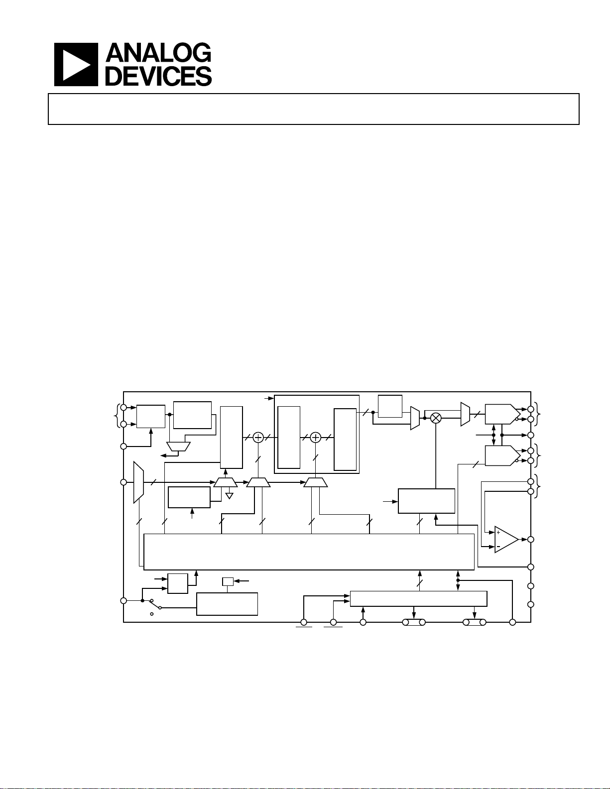
FUNCTIONAL BLOCK DIAGRAM
SYSTEM CLOCK
ACC 1
FREQUENCY
ACCUMULATOR
MUX
FREQUENCY
TUNING
WORD 1
÷2
INTERNAL
PROGRAMMABLE
UPDATE CLOCK
48
48
48
MUX MUX
FREQUENCY
TUNING
WORD 2
PROGRAMMING REGISTERS
SYSTEM
CLOCK
Frequency ramped FSK
<25 ps rms total jitter in clock generator mode
Automatic bidirectional frequency sweeping
Sin(x)/x correction
Simplified control interface
10 MHz serial 2-wire or 3-wire SPI-compatible
100 MHz parallel 8-bit programming
3.3 V single supply
Multiple power-down functions
Single-ended or differential input reference clock
Small, 80-lead LQFP or TQFP with exposed pad
APPLICATIONS
Agile LO frequency synthesis
Programmable clock generator
FM chirp source for radar and scanning systems
Test and measurement equipment
Commercial and amateur RF exciter
DDS CORE
17
17
ACC 2
PHASE
ACCUMULATOR
FIRST 14-BIT
PHASE/OFFSET
WORD
READ WRITE SERIAL/
Figure 1.
14
AD9852
PHASE-TO-
SECOND 14-BIT
12
SINC
FILTER
I
AMPLITUDE
CONVERTER
Q
SYSTEM
CLOCK
14
PHASE/OFFSET
WORD
PARALLEL
SELECT
DIGITAL MULTIPLIERS
INV
MUX
PROGRAMMABLE
AMPLITUDE AND
RATE CONTROL
12
AM
MODULATION
BUS
I/O PORT BUFFERS
6-BIT ADDRESS
OR SERIAL
PROGRAMMING
LINES
MUX
SYSTEM
CLOCK
12-BIT DC
CONTROL
PARALLEL
12
12
8-BIT
LOAD
AD9852
12-BIT
COSINE
DAC
12-BIT
CONTROL
DAC
COMPARATOR
MASTER
RESET
ANALOG
OUT
DAC R
ANALOG
OUT
ANALOG
IN
CLOCK
OUT
OSK
GND
+V
S
SET
00634-001
Rev. E
Information furnished by Analog Devices is believed to be accurate and reliable. However, no
responsibility is assumed by Anal og Devices for its use, nor for any infringements of patents or ot her
rights of third parties that may result from its use. Specifications subject to change without notice. No
license is granted by implication or otherwise under any patent or patent rights of Analog Devices.
Trademarks and registered trademarks are the property of their respective owners.
One Technology Way, P.O. Box 9106, Norwood, MA 02062-9106, U.S.A.
Tel: 781.329.4700 www.analog.com
Fax: 781.461.3113 ©2002–2007 Analog Devices, Inc. All rights reserved.

AD9852
TABLE OF CONTENTS
Features .............................................................................................. 1
Inverse Sinc Function ................................................................ 29
Applications....................................................................................... 1
Functional Block Diagram .............................................................. 1
Revision History ............................................................................... 3
General Description......................................................................... 4
Overview........................................................................................ 4
Specifications..................................................................................... 5
Absolute Maximum Ratings............................................................ 8
Thermal Resistance ...................................................................... 8
Explanation of Test Levels........................................................... 8
ESD Caution.................................................................................. 8
Pin Configuration and Function Descriptions............................. 9
Typical Performance Characteristics ........................................... 12
Typical Applicat i o n s ....................................................................... 16
Modes of Operation ....................................................................... 18
Single Tone (Mode 000)............................................................. 18
REFCLK Multiplier.................................................................... 29
High Speed Comparator............................................................ 30
Power-Down ............................................................................... 30
Programming the AD9852............................................................ 31
MASTER RESET ........................................................................ 31
Parallel I/O Operation ............................................................... 31
Serial Port I/O Operation.......................................................... 31
General Operation of the Serial Interface................................... 34
Instruction Byte .......................................................................... 34
Serial Interface Port Pin Descriptions..................................... 35
MSB/LSB Transfers .................................................................... 35
Control Register Descriptions.................................................. 36
Power Dissipation and Thermal Considerations....................... 38
Thermal Impedance................................................................... 38
Junction Temperature Considerations .................................... 38
Unramped FSK (Mode 001)...................................................... 19
Ramped FSK (Mode 010).......................................................... 19
Chirp (Mode 011)....................................................................... 22
BPSK (Mode 100)....................................................................... 26
Using the AD9852 .......................................................................... 27
Internal and External Update Clock........................................ 27
On/Off Output Shaped Keying (OSK) .................................... 27
Cosine DAC ................................................................................ 29
Control DAC............................................................................... 29
Evaluation of Operating Conditions ............................................ 40
Thermally Enhanced Package Mounting Guidelines............ 40
Evaluation Board ............................................................................ 41
Evaluation Board Instructions.................................................. 41
General Operating Instructions ............................................... 41
Using the Provided Software .................................................... 43
Support ........................................................................................ 43
Outline Dimensions ....................................................................... 51
Ordering Guide .......................................................................... 52
Rev. E | Page 2 of 52

AD9852
REVISION HISTORY
5/07—Rev. D to Rev. E
Changed AD9852ASQ to AD9852ASVZ ....................... Universal
Changed AD9852AST to AD9852ASTZ.........................Universal
Change to Features............................................................................1
Changes to Endnote 10 of Table 1...................................................7
Changes to Absolute Maximum Ratings........................................8
Added Thermal Resistance Section ................................................8
Change to Ramped FSK (Mode 010) Section..............................19
Change to Internal and External Update Clock Section............27
Change to Thermal Impedance Section.......................................38
Changes to Junction Temperature Considerations Section.......38
Changes to Thermally Enhanced Package Mounting
Guidelines Section......................................................................40
Deleted Figure 61 to Figure 64 ......................................................41
Changes to Table 14 ........................................................................44
Updated Outline Dimensions........................................................51
Changes to Ordering Guide...........................................................52
12/05—Rev. C to Rev. D
Updated Format.................................................................. Universal
Changes to General Description .....................................................4
Changes to Explanation of Test Levels Section .............................9
Change to Pin Configuration ........................................................10
Changes to Figure 65 ......................................................................47
Changes to Outline Dimensions ...................................................52
Changes to Ordering Guide...........................................................52
3/02—Rev. A to Rev. B
Changes to General Description.....................................................1
Changes to Functional Block Diagram .......................................... 1
Changes to Specifications ................................................................3
Changes to Absolute Maximum Ratings........................................5
Changes to Pin Function Descriptions ..........................................6
Changes to Figure 3 ..........................................................................8
Deleted Two TPCs ..........................................................................11
Changes to Figure 18 and Figure 19 .............................................11
Changes to BPDK Mode Section .................................................. 21
Changes to Differential Refclk Enable Section ...........................24
Changes to Master Reset Section..................................................24
Changes to Parallel I/O Operation Section .................................24
Changes to General Operation of the Serial
Interface Section..............................................................................27
Changes to Figure 50 ......................................................................27
Changes to Figure 65 ......................................................................36
4/04—Rev. B to Rev. C
Updated Format.................................................................. Universal
Changes to Figure 1...........................................................................1
Changes to General Description .....................................................3
Changes to Table 1 ............................................................................4
Changes to Footnote 2......................................................................6
Changes to Figure 2...........................................................................8
Changes to Table 5 ..........................................................................17
Changes to Equation in Ramped FSK (Mode 010).....................19
Changes to Evaluation Board Instructions ..................................39
Changes to General Operating Instructions Section..................39
Changes to Using the Provided Software Section.......................42
Changes to Figure 65 ......................................................................43
Changes to Figure 66 ......................................................................44
Changes to Figure 72 and Figure 73 .............................................48
Changes to Ordering Guide...........................................................48
Rev. E | Page 3 of 52

AD9852
GENERAL DESCRIPTION
The AD9852 digital synthesizer is a highly integrated device
that uses advanced DDS technology, coupled with an internal
high speed, high performance D/A converter to form a digitally
programmable, agile synthesizer function. When referenced to
an accurate clock source, the AD9852 generates a highly stable
frequency-, phase-, and amplitude-programmable cosine output
that can be used as an agile LO in communications, radar, and
many other applications. The innovative high speed DDS core
of the AD9852 provides 48-bit frequency resolution (1 µHz
tuning resolution with 300 MHz SYSCLK). Maintaining 17 bits
ensures excellent SFDR.
The circuit architecture of the AD9852 allows the generation of
output signals at frequencies up to 150 MHz, which can be
digitally tuned at a rate of up to 100 million new frequencies
per second. The (externally filtered) cosine wave output can be
converted to a square wave by the internal comparator for agile
clock generator applications. The device provides two 14-bit
phase registers and a single pin for BPSK operation.
For higher-order PSK operation, the I/O interface can be used
for phase changes. The 12-bit cosine DAC, coupled with the
innovative DDS architecture, provides excellent wideband and
narrow-band output SFDR. When configured with the
comparator, the 12-bit control DAC facilitates static duty cycle
control in the high speed clock generator applications.
The 12-bit digital multiplier permits programmable amplitude
modulation, on/off output shaped keying, and precise amplitude
control of the cosine DAC output. Chirp functionality is also
included for wide bandwidth frequency sweeping applications.
The AD9852 programmable 4× to 20× REFCLK multiplier circuit internally generates the 300 MHz system clock from a lower
frequency external reference clock. This saves the user the expense
and difficulty of implementing a 300 MHz system clock source.
Direct 300 MHz clocking is also accommodated with either singleended or differential inputs. Single-pin, conventional FSK and the
enhanced spectral qualities of ramped FSK are supported. The
AD9852 uses advanced 0.35 CMOS technology to provide this
high level of functionality on a single 3.3 V supply.
The AD9852 is pin-for-pin compatible with the
tone synthesizer. The AD9852 is specified to operate over the
extended industrial temperature range of −40°C to +85°C.
AD9854 single-
OVERVIEW
The AD9852 digital synthesizer is a highly flexible device that
addresses a wide range of applications. The device consists of
an NCO with a 48-bit phase accumulator, a programmable
reference clock multiplier, an inverse sinc filter, a digital
multiplier, two 12-bit/300 MHz DACs, a high speed analog
comparator, and an interface logic. This highly integrated
device can be configured to serve as a synthesized LO agile
clock generator and FSK/BPSK modulator. The theory of
operation for the functional blocks of the device and a technical
description of the signal flow through a DDS device is provided
by Analog Devices, Inc., in the tutorial
Digital Signal Synthesis
applications information for a variety of digital synthesis
implementations.
. The tutorial also provides basic
A Technical Tutorial on
Rev. E | Page 4 of 52

AD9852
SPECIFICATIONS
VS = 3.3 V ± 5%, R
external reference clock frequency = 20 MHz with REFCLK multiplier enabled at 10× for AD9852ASTZ, unless otherwise noted.
Table 1.
Test AD9852ASVZ AD9852ASTZ
Parameter Temp Level Min Typ Max Min Typ Max Unit
REFERENCE CLOCK INPUT CHARACTERISTICS1
Internal System Clock Frequency Range
REFCLK Multiplier Enabled Full VI 20 300 20 200 MHz
REFCLK Multiplier Disabled Full VI DC 300 DC 200 MHz
External Reference Clock Frequency Range
REFCLK Multiplier Enabled Full VI 5 75 5 50 MHz
REFCLK Multiplier Disabled Full VI DC 300 DC 200 MHz
Duty Cycle 25°C IV 45 50 55 45 50 55 %
Input Capacitance 25°C IV 3 3 pF
Input Impedance 25°C IV 100 100 kΩ
Differential Common-Mode Voltage Range
Minimum Signal Amplitude2 25°C IV 400 400 mV p-p
Common-Mode Range 25°C IV 1.6 1.75 1.9 1.6 1.75 1.9 V
VIH (Single-Ended Mode) 25°C IV 2.3 2.3 V
VIL (Single-Ended Mode) 25°C IV 1 1 V
DAC STATIC OUTPUT CHARACTERISTICS
Output Update Speed Full I 300 200 MSPS
Resolution 25°C IV 12 12 Bits
Cosine and Control DAC Full-Scale Output Current 25°C IV 5 10 20 5 10 20 mA
Gain Error 25°C I −6
Output Offset 25°C I 2 2 μA
Differential Nonlinearity 25°C I 0.3 1.25 0.3 1.25 LSB
Integral Nonlinearity 25°C I 0.6 1.66 0.6 1.66 LSB
Output Impedance 25°C IV 100 100 kΩ
Voltage Compliance Range 25°C I −0.5 +1.0 −0.5 +1.0 V
DAC DYNAMIC OUTPUT CHARACTERISTICS
DAC Wideband SFDR
1 MHz to 20 MHz A
20 MHz to 40 MHz A
40 MHz to 60 MHz A
60 MHz to 80 MHz A
80 MHz to 100 MHz A
100 MHz to 120 MHz A
DAC Narrow-Band SFDR
10 MHz A
10 MHz A
10 MHz A
41 MHz A
41 MHz A
41 MHz A
OUT
OUT
OUT
OUT
OUT
OUT
119 MHz A
119 MHz A
119 MHz A
= 3.9 kΩ, external reference clock frequency = 30 MHz with REFCLK multiplier enabled at 10× for AD9852ASVZ,
SET
+2.2
5
25°C V 58 58 dBc
OUT
25°C V 56 56 dBc
OUT
25°C V 52 52 dBc
OUT
25°C V 48 48 dBc
OUT
OUT
25°C V 48 dBc
OUT
25°C V 48 48 dBc
−6
+2.2
5
(±1 MHz) 25°C V 83 83 dBc
(±250 kHz) 25°C V 83 83 dBc
(±50 kHz) 25°C V 91 91 dBc
(±1 MHz) 25°C V 82 82 dBc
(±250 kHz) 25°C V 84 84 dBc
(±50 kHz) 25°C V 89 89 dBc
(±1 MHz) 25°C V 71 dBc
OUT
(±250 kHz) 25°C V 77 dBc
OUT
(±50 kHz) 25°C V 83 dBc
OUT
% FS
Rev. E | Page 5 of 52

AD9852
Test AD9852ASVZ AD9852ASTZ
Parameter Temp Level Min Typ Max Min Typ Max Unit
Residual Phase Noise
(A
= 5 MHz, External Clock = 30 MHz,
OUT
REFCLK Multiplier Engaged at 10×)
1 kHz Offset 25°C V 140 140 dBc/Hz
10 kHz Offset 25°C V 138 138 dBc/Hz
100 kHz Offset 25°C V 142 142 dBc/Hz
(A
= 5 MHz, External Clock = 300 MHz,
OUT
REFCLK Multiplier Bypassed)
1 kHz Offset 25°C V 142 142 dBc/Hz
0 kHz Offset 25°C V 148 148 dBc/Hz
100 kHz Offset 25°C V 152 152 dBc/Hz
PIPELINE DELAYS3, 4,
5
DDS Core (Phase Accumulator and
Phase-to-Amp Converter)
Frequency Accumulator 25°C IV 26 26 SYSCLK cycles
Inverse Sinc Filter 25°C IV 16 16 SYSCLK cycles
Digital Multiplier 25°C IV 9 9 SYSCLK cycles
DAC 25°C IV 1 1 SYSCLK cycles
I/O Update Clock (Internal Mode) 25°C IV 2 2 SYSCLK cycles
I/O Update Clock (External Mode) 25°C IV 3 3 SYSCLK cycles
MASTER RESET DURATION 25°C IV 10 10 SYSCLK cycles
COMPARATOR INPUT CHARACTERISTICS
Input Capacitance 25°C V 3 3 pF
Input Resistance 25°C IV 500 500 kΩ
Input Current 25°C I ± 1 ± 5 ± 1 ± 5 μA
Hysteresis 25°C IV 10 20 10 20 mV p-p
COMPARATOR OUTPUT CHARACTERISTICS
Logic 1 Voltage, High-Z Load Full VI 3.1 3.1 V
Logic 0 Voltage, High-Z Load Full VI 0.16 0.16 V
Output Power, 50 Ω Load, 120 MHz Toggle Rate 25°C I 9 11 9 11 dBm
Propagation Delay 25°C IV 3 3 ns
Output Duty Cycle Error6 25°C I −10 ± 1 +10 −10 ± 1 +10 %
Rise/Fall Time, 5 pF Load 25°C V 2 2 ns
Toggle Rate, High-Z Load 25°C IV 300 350 300 350 MHz
Toggle Rate, 50 Ω Load 25°C IV 375 400 375 400 MHz
Output Cycle-to-Cycle Jitter7 25°C IV 4.0 4.0 ps rms
COMPARATOR NARROW-BAND SFDR
8
10 MHz (±1 MHz) 25°C V 84 84 dBc
10 MHz (±250 MHz) 25°C V 84 84 dBc
10 MHz (±50 kHz) 25°C V 92 92 dBc
41 MHz (±1 MHz) 25°C V 76 76 dBc
41 MHz (±250 kHz) 25°C V 82 82 dBc
41 MHz (±50 kHz) 25°C V 89 89 dBc
119 MHz (±1 MHz) 25°C V 73 dBc
119 MHz (±250 kHz) 25°C V 73 dBc
119 MHz (±50 kHz) 25°C V 83 dBc
CLOCK GENERATOR OUTPUT JITTER
5 MHz A
40 MHz A
100 MHz A
25°C V 23 23 ps rms
OUT
25°C V 12 12 ps rms
OUT
25°C V 7 7 ps rms
OUT
8
25°C IV 33 33 SYSCLK cycles
Rev. E | Page 6 of 52

AD9852
Test AD9852ASVZ AD9852ASTZ
Parameter Temp Level Min Typ Max Min Typ Max Unit
PARALLEL I/O TIMING CHARACTERISTICS
t
(Address Setup Time to WR Signal Active)
ASU
t
(Address Hold Time to WR Signal Inactive)
ADHW
t
(Data Setup Time to WR Signal Inactive)
DSU
t
(Data Hold Time to WR Signal Inactive)
DHD
t
(WR Signal Minimum Low Time)
WRLOW
t
(WR Signal Minimum High Time)
WRHIGH
tWR (Minimum WR Time)
t
(Address to Data Valid Time) Full V 15 15 15 15 ns
ADV
t
(Address Hold Time to RD Signal Inactive)
ADHR
t
(RD Low to Output Valid)
RDLOV
t
(RD High to Data Three-State)
RDHOZ
SERIAL I/O TIMING CHARACTERISTICS
t
(CS Setup Time)
PRE
t
(Period of Serial Data Clock) Full IV 100 100 ns
SCLK
t
(Serial Data Setup Time) Full IV 30 30 ns
DSU
t
(Serial Data Clock Pulse Width High) Full IV 40 40 ns
SCLKPWH
t
(Serial Data Clock Pulse Width Low) Full IV 40 40 ns
SCLKPWL
t
(Serial Data Hold Time) Full IV 0 0 ns
DHLD
tDV (Data Valid Time) Full V 30 30 ns
CMOS LOGIC INPUTS 9
Logic 1 Voltage 25°C I 2.2 2.2 V
Logic 0 Voltage 25°C I 0.8 0.8 V
Logic 1 Current 25°C IV ± 5 ± 12 μA
Logic 0 Current 25°C IV ± 5 ± 12 μA
Input Capacitance 25°C V 3 3 pF
POWER SUPPLY
10
VS Current11 25°C I 815 922 585 660 mA
VS Current12 25°C I 640 725 465 520 mA
VS Current13 25°C I 585 660 425 475 mA
11
P
DISS
12
P
DISS
13
P
DISS
P
Power-Down Mode 25°C I 1 50 1 50 mW
DISS
1
The reference clock inputs are configured to accept a 1 V p-p (typical) dc offset square or sine waves centered at one-half the applied VDD or a 3 V TTL-level pulse input.
2
An internal 400 mV p-p differential voltage swing equates to 200 mV p-p applied to both REFCLK input pins.
3
Pipeline delays of each individual block are fixed; however, if the first eight MSBs of a tuning word are all 0s, the delay appears longer. This is due to insufficient phase
accumulation per a system clock period to produce enough LSB amplitude to the D/A converter.
4
If a feature such as inverse sinc, which has 16 pipeline delays, can be bypassed, the total delay is reduced by that amount.
5
The I/O UD CLK transfers data from the I/O port buffers to the programming registers. This transfer is measured in system clocks.
6
A change in duty cycle from 1 MHz to 100 MHz with 1 V p-p sine wave input and 0.5 V threshold.
7
Represents the comparator’s inherent cycle-to-cycle jitter contribution. The input signal is a 1 V, 40 MHz square wave, and the measurement device is a Wavecrest DTS-2075.
8
Comparator input originates from analog output section via external 7-pole elliptic low-pass filter. Single-ended input, 0.5 V p-p. Comparator output terminated in 50 Ω.
9
Avoid overdriving digital inputs. (Refer to equivalent circuits in Figure 3.)
10
If all device functions are enabled, it is not recommended to simultaneously operate the device at the maximum ambient temperature of 85°C and at the maximum
internal clock frequency. This configuration may result in violating the maximum die junction temperature of 150°C. Refer to the Power Dissipation and Thermal
Considerations section for derating and thermal management information.
11
All functions engaged.
12
All functions except inverse sinc engaged.
13
All functions except inverse sinc and digital multipliers engaged.
Full IV 8.0 7.5 8.0 7.5 ns
Full IV 0 0 ns
Full IV 3.0 1.6 3.0 1.6 ns
Full IV 0 0 ns
Full IV 2.5 1.8 2.5 1.8 ns
Full IV 7 7 ns
Full IV 10.5 10.5 ns
Full IV 5 5 ns
Full IV 15 15 ns
Full IV 10 10 ns
Full IV 30 30 ns
25°C I 2.70 3.20 1.93 2.39 W
25°C I 2.12 2.52 1.53 1.81 W
25°C I 1.93 2.29 1.40 1.65 W
Rev. E | Page 7 of 52
AD9852
ABSOLUTE MAXIMUM RATINGS
Table 2.
Parameter Rating
Maximum Junction Temperature 150°C
V
S
Digital Inputs −0.7 V to +V
4 V
S
Digital Output Current 5 mA
Storage Temperature −65°C to +150°C
Operating Temperature −40°C to +85°C
Lead Temperature (Soldering, 10 sec) 300°C
Maximum Clock Frequency (ASVZ) 300 MHz
Maximum Clock Frequency (ASTZ) 200 MHz
Stresses above those listed under Absolute Maximum Ratings
may cause permanent damage to the device. This is a stress
rating only; functional operation of the device at these or any
other conditions above those indicated in the operational
section of this specification is not implied. Exposure to absolute
maximum rating conditions for extended periods may affect
device reliability.
THERMAL RESISTANCE
The heat sink of the AD9852ASVZ 80-lead TQFP package must
be soldered to the PCB.
Table 3.
Thermal Characteristic TQFP LQFP
θJA (0 m/sec airflow)
θ
(1.0 m/sec airflow)
JMA
θ
(2.5 m/sec airflow)
JMA
1, 2
Ψ
JT
6, 7
θ
JC
1
Per JEDEC JESD51-2 (heat sink soldered to PCB).
2
2S2P JEDEC test board.
3
Values of θJA are provided for package comparison and PCB design
considerations.
4
Per JEDEC JESD51-6 (heat sink soldered to PCB).
5
Airflow increases heat dissipation, effectively reducing θJA. Furthermore, the
more metal that is directly in contact with the package leads from metal
traces through holes, ground, and power planes, the more θJA is reduced.
6
Per MIL-Std 883, Method 1012.1.
7
Values of θJC are provided for package comparison and PCB design
considerations when an external heat sink is required.
1, 2, 3
2, 3, 4, 5
2, 3, 4, 5
16.2°C/W 38°C/W
13.7°C/W
12.8°C/W
0.3°C/W
2.0°C/W
To determine the junction temperature on the application PCB
use the following equation:
T
= T
+ (
Ψ
J
case
× PD)
JT
where:
is the junction temperature expressed in degrees Celsius.
T
J
is the case temperature expressed in degrees Celsius, as
T
case
measured by the user at the top center of the package.
Ψ
= 0.3°C/W.
JT
PD is the power dissipation (PD); see the
Thermal Considerations
section for the method to calculate PD.
Power Dissipation and
EXPLANATION OF TEST LEVELS
Table 4.
Test Level Description
I 100% production tested.
III Sample tested only.
IV
Parameter is guaranteed by design and
characterization testing.
V Parameter is a typical value only.
VI
Devices are 100% production tested at 25°C and
guaranteed by design and characterization testing
for industrial operating temperature range.
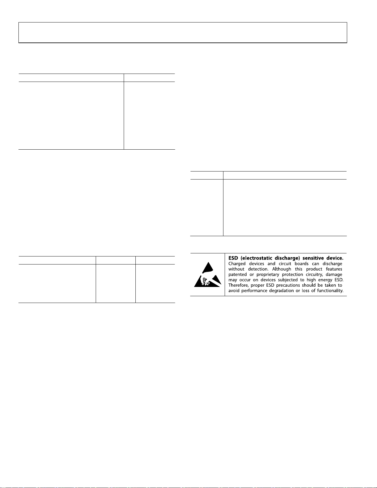
ESD CAUTION
Rev. E | Page 8 of 52
AD9852
PIN CONFIGURATION AND FUNCTION DESCRIPTIONS
DVDD79DVDD78DGND77DGND76DGND75DGND74DVDD73DVDD72DGND71MASTER RESET70S/P SELECT69REFCLK68REFCLK67AGND66AGND65AVDD64DIFF CLK ENABLE63NC62AGND61PLL FILTER
80
1
D7
2
D6
3
D5
4
D4
5
D3
6
D2
7
D1
8
D0
9
DVDD
10
DVDD
11
DGND
12
DGND
13
NC
14
A5
15
A4
16
A3
A1/SDO
A0/SDIO
17
18
19
20
A2/IO RESET
I/O UD CLK
NC = NO CONNECT
60
PIN 1
AD9852
TOP VIEW
(Not to Scale)
21
22
23
RD/CS
WR/SCLK
DVDD24DVDD25DVDD
26
DGND27DGND28DGND
29
FSK/BPSK/HOLD
30
OSK
31
AVDD32AVDD
33
AGND34AGND
35NC36
VOUT
37
AVDD38AVDD
39
AGND40AGND
59
58
57
56
55
54
53
52
51
50
49
48
47
46
45
44
43
42
41
AVDD
AGND
NC
NC
DAC R
DACBP
AVDD
AGND
IOUT2
IOUT2
AVDD
IOUT1
IOUT1
AGND
AGND
AGND
AVDD
VINN
VINP
AGND
SET
00634-002
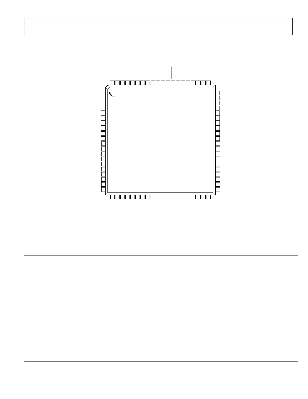
Figure 2. Pin Configuration
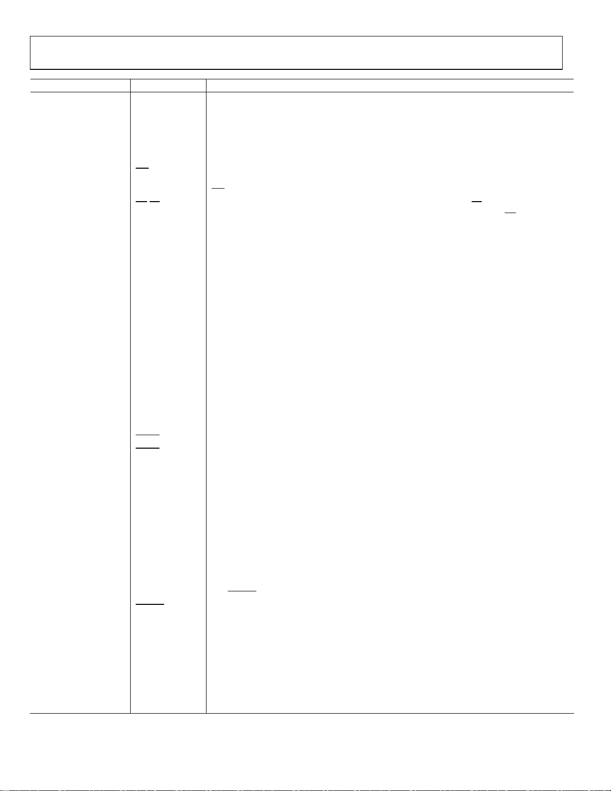
Table 5. Pin Function Descriptions
Pin Number Mnemonic Description
1 to 8 D7 to D0 8-Bit Bidirectional Parallel Programming Data Inputs. Used only in parallel programming mode.
9, 10, 23, 24, 25,
73, 74, 79, 80
11, 12, 26, 27, 28,
DVDD
Connections for the Digital Circuitry Supply Voltage. Nominally 3.3 V more positive than AGND
and DGND.
DGND Connections for Digital Circuitry Ground Return. Same potential as AGND.
72, 75 to 78
13, 35, 57, 58, 63 NC No Internal Connection.
14 to 16 A5 to A3
Parallel Address Inputs for Program Registers (Part of 6-Bit Parallel Address Inputs for Program
Register, A5:A0). Used only in parallel programming mode.
17 A2/IO RESET
Parallel Address Input for Program Registers (Part of 6-Bit Parallel Address Inputs for Program
Register, A5:A0)/IO Reset. A2 is used only in parallel programming mode. IO RESET is used when
the serial programming mode is selected, allowing an IO RESET of the serial communication bus
that is unresponsive due to improper programming protocol. Resetting the serial bus in this
manner does not affect previous programming, nor does it invoke the default programming
18 A1/SDO
values seen in
Parallel Address Input for Program Registers (Part of 6-Bit Parallel Address Inputs for Program
Table 9 . Active high.
Register, A5:A0)/Unidirectional Serial Data Output. A1 is used only in parallel programming
mode. SDO is used in 3-wire serial communication mode when the serial programming mode is
selected.
Rev. E | Page 9 of 52
AD9852
Pin Number Mnemonic Description
19 A0/SDIO
20 I/O UD CLK
21
22
WR/SCLK Write Parallel Data to I/O Port Buffers. Shared function with SCLK. Serial clock signal associated
RD/CS Read Parallel Data from Programming Registers. Shared function with CS. Chip select signal
29 FSK/BPSK/HOLD
30 OSK
31, 32, 37, 38, 44, 50, 54,
AVDD
60, 65
33, 34, 39, 40, 41, 45, 46,
AGND Connections for Analog Circuitry Ground Return. Same potential as DGND.
47, 53, 59, 62, 66, 67
36 VOUT
42 VINP Voltage Input Positive. The noninverting input of the internal high speed comparator.
43 VINN Voltage Input Negative. The inverting input of the internal high speed comparator.
48 IOUT1 Unipolar Current Output of the Cosine DAC (refer to Figure 3).
49
51
IOUT1
IOUT2
52 IOUT2 Unipolar Current Output of the Control DAC.
55 DACBP
56 DAC R
SET
61 PLL FILTER
64 DIFF CLK ENABLE
68
REFCLK Complementary (180° Out of Phase) Differential Clock Signal. User should tie this pin high or
69 REFCLK
70 S/P SELECT
71 MASTER RESET
Parallel Address Input for Program Registers (Part of 6-Bit Parallel Address Inputs for Program
Register, A5:A0)/Bidirectional Serial Data Input/Output. A0 is used only in parallel programming
mode. SDIO is used in 2-wire serial communication mode.
Bidirectional I/O Update Clock. Direction is selected in control register. If selected as an input, a
rising edge transfers the contents of the I/O port buffers to the programming registers. If I/O UD
CLK is selected as an output (default), an output pulse (low to high) with a duration of eight
system clock cycles indicates that an internal frequency update has occurred.
with the serial programming bus. Data is registered on the rising edge. This pin is shared with
WR when the parallel mode is selected. The mode is dependent on Pin 70 (S/P SELECT).
associated with the serial programming bus. Active low. This pin is shared with
RD when the
parallel mode is selected.
Multifunction Pin. Functions according to the mode of operation selected in the programming
control register. If in the FSK mode, logic low selects F1 and logic high selects F2. If in the BPSK
mode, logic low selects Phase 1 and logic high selects Phase 2. In chirp mode, logic high
engages the hold function, causing the frequency accumulator to halt at its current location. To
resume or commence chirp, logic low is asserted.
Output Shaped Keying. Must first be selected in the programming control register to function.
A logic high causes the cosine DAC outputs to ramp up from zero-scale to full-scale amplitude
at a preprogrammed rate. Logic low causes the full-scale output to ramp down to zero scale at
the preprogrammed rate.
Connections for the Analog Circuitry Supply Voltage. Nominally 3.3 V more positive than AGND
and DGND.
Noninverted Output of the Internal High Speed Comparator. Designed to drive 10 dBm to 50 Ω
loads as well as standard CMOS logic levels.
Complementary Unipolar Current Output of the Cosine DAC.
Complementary Unipolar Current Output of the Control DAC.
Common Bypass Capacitor Connection for Both DACs. A 0.01 μF chip capacitor from this pin to
AVDD improves harmonic distortion and SFDR slightly. No connect is permissible, but results in
a slight degradation in SFDR.
Common Connection for Both DACs. Used to set the full-scale output current. R
Normal R
range is from 8 kΩ (5 mA) to 2 kΩ (20 mA).
SET
= 39.9/ I
SET
OUT
Connection for the External Zero-Compensation Network of the REFCLK Multiplier’s PLL Loop
Filter. The zero-compensation network consists of a 1.3 kΩ resistor in series with a 0.01 μF
capacitor. The other side of the network should be connected to AVDD as close as possible to
Pin 60. For optimum phase noise performance, the REFCLK multiplier can be bypassed by
setting the bypass PLL bit in Control Register 1E hex.
Differential REFCLK Enable. A high level of this pin enables the differential clock inputs, REFCLK
REFCLK (Pin 69 and Pin 68, respectively).
and
low when single-ended clock mode is selected. Same signal levels as REFCLK.
Single-Ended (CMOS Logic Levels Required) Reference Clock Input or One of Two Differential
Clock Signals. In differential reference clock mode, both inputs can be CMOS logic levels or have
greater than 400 mV p-p square or sine waves centered about 1.6 V dc.
Selects between serial programming mode (logic low) and parallel programming mode
(logic high).
Initializes the serial/parallel programming bus to prepare for user programming, and sets
programming registers to a do-nothing state defined by the default values listed in
Table 9.
Active on logic high. Asserting this pin is essential for proper operation upon power-up.
.
Rev. E | Page 10 of 52
AD9852
V
.
MUST TERMINATE OUTPUTS
FOR CURRENT FLOW. DO
NOT EXCEED THE OUTPUT
OLTAGE COMPLIANCE RATING
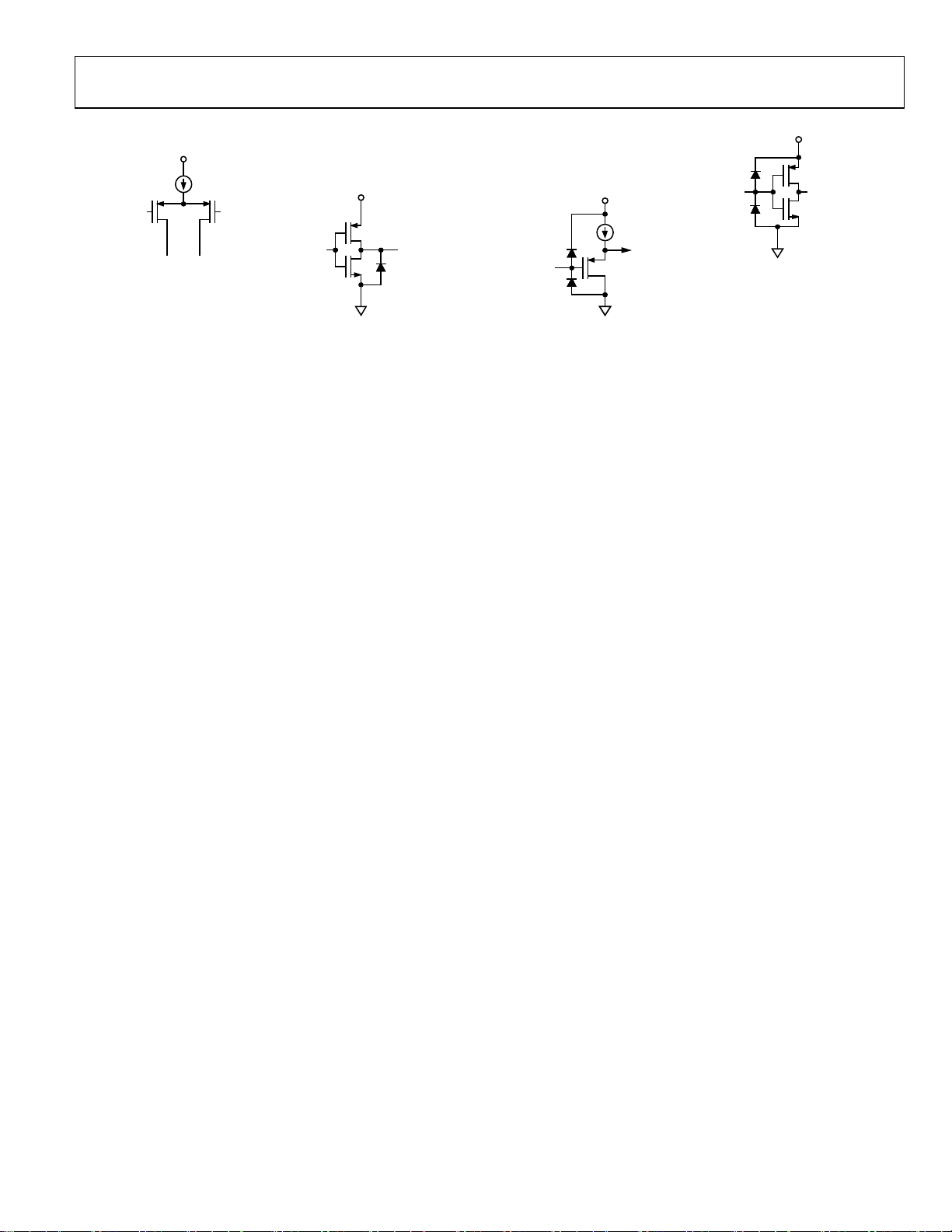
A. DAC Outputs B. Comparator Output C. Comparator Input D. Digital Inputs
AVDD
I
OUTIOUTB
AVDD
VINP/
COMPARATOR
OUT
VINN
Figure 3. Equivalent Input and Output Circuits
AVDD
DVDD
DIGITAL
IN
AVOID OVERDRIVING
DIGITAL INPUTS. FORWARD
BIASING ESD DIODES MAY
COUPLE DIGITAL NOISE
ONTO POWER PINS.
00634-003
Rev. E | Page 11 of 52
AD9852
–
–
–
–
–
–
TYPICAL PERFORMANCE CHARACTERISTICS
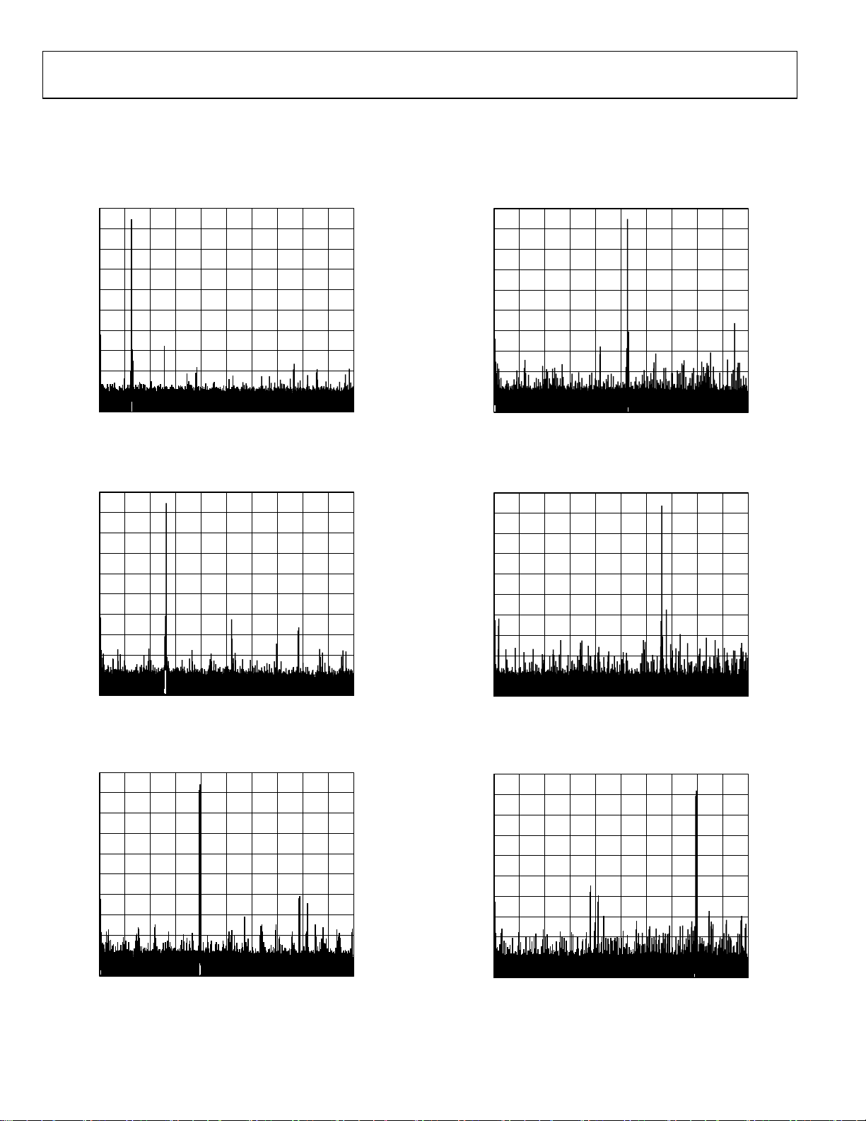
Figure 4 to Figure 9 indicate the wideband harmonic distortion performance of the AD9852 from 19.1 MHz to 119.1 MHz fundamental
output, reference clock = 30 MHz, REFCLK multiplier = 10×. Each graph is plotted from 0 MHz to 150 MHz (Nyquist).
0
–10
–20
–30
–40
–50
–60
–70
–80
–90
100
START 0Hz
0
–10
–20
–30
–40
–50
–60
–70
–80
–90
100
START 0Hz
15MHz/ STOP 150MHz
Figure 4. Wideband SFDR, 19.1 MHz
15MHz/ STOP 150MHz
Figure 5. Wideband SFDR, 39.1 MHz
00634-004
00634-005
0
–10
–20
–30
–40
–50
–60
–70
–80
–90
100
START 0Hz
0
–10
–20
–30
–40
–50
–60
–70
–80
–90
100
START 0Hz
15MHz/ STOP 150MHz
Figure 7. Wideband SFDR, 79.1 MHz
15MHz/ STOP 150MHz
Figure 8. Wideband SFDR, 99.1 MHz
00634-007
00634-008
0
–10
–20
–30
–40
–50
–60
–70
–80
–90
100
START 0Hz
15MHz/ STOP 150MHz
Figure 6. Wideband SFDR, 59.1 MHz
00634-006
0
–10
–20
–30
–40
–50
–60
–70
–80
–90
100
START 0Hz
15MHz/ STOP 150MHz
Figure 9. Wideband SFDR, 119.1 MHz
00634-009
Rev. E | Page 12 of 52
AD9852
–
–
–
–
–
–
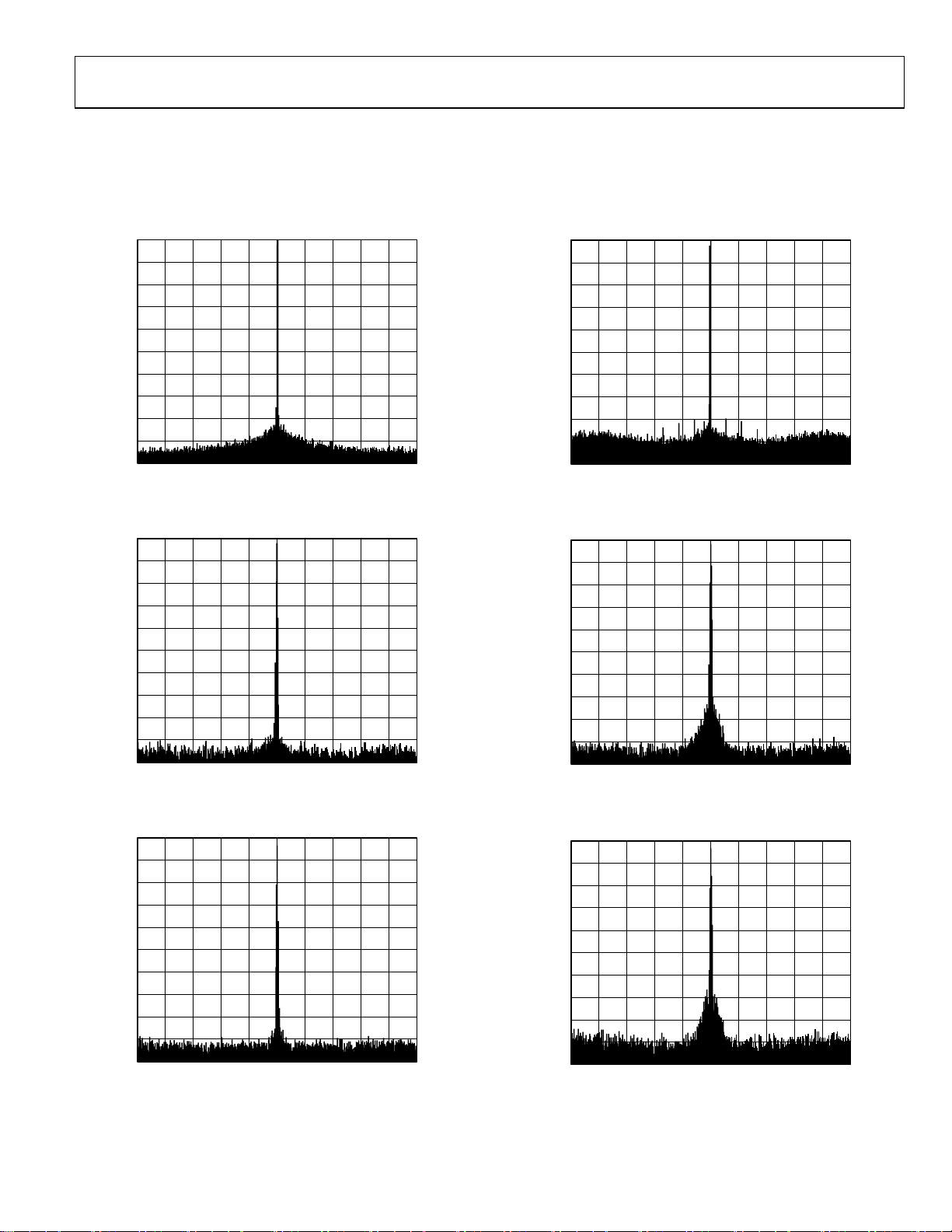
Figure 10 to Figure 15 show the trade-off in elevated noise floor, increased phase noise (PN), and discrete spurious energy when the
internal REFCLK multiplier circuit is engaged. Plots with wide (1 MHz) and narrow (50 kHz) spans are shown. Compare the noise floor of
Figure 11 and Figure 12 with that of Figure 14 and Figure 15. The improvement seen in Figure 11 and Figure 12 is a direct result of sampling
the fundamental at a higher rate. Sampling at a higher rate spreads the quantization noise of the DAC over a wider bandwidth, which
effectively lowers the noise floor.
0
–10
–20
–30
–40
–50
–60
–70
–80
–90
100
CENTER 39.1MHz
100kHz/ SPAN 1MHz
Figure 10. Narrow-Band SFDR, 39.1 MHz, 1 MHz BW,
300 MHz REFCLK with REFCLK Multiplier Bypassed
0
–10
–20
–30
–40
–50
–60
–70
–80
–90
100
CENTER 39.1MHz
5kHz/ SPAN 50kHz
Figure 11. Narrow-Band SFDR, 39.1 MHz, 50 kHz BW,
300 MHz REFCLK with REFCLK Multiplier Bypassed
0
–10
–20
–30
–40
–50
–60
–70
–80
–90
100
CENTER 39.1MHz
5kHz/ SPAN 50kHz
Figure 12. Narrow-Band SFDR, 39.1 MHz, 50 kHz BW,
100 MHz REFCLK with REFCLK Multiplier Bypassed
00634-010
00634-011
00634-012
0
–10
–20
–30
–40
–50
–60
–70
–80
–90
100
CENTER 39.1MHz
100kHz/ SPAN 1MHz
Figure 13. Narrow-Band SFDR, 39.1 MHz, 1 MHz BW,
30 MHz REFCLK with REFCLK Multiplier = 10×
0
–10
–20
–30
–40
–50
–60
–70
–80
–90
100
CENTER 39.1MHz
5kHz/ SPAN 50kHz
Figure 14. Narrow-Band SFDR, 39.1 MHz, 50 kHz BW,
30 MHz REFCLK with REFCLK Multiplier = 10×
0
–10
–20
–30
–40
–50
–60
–70
–80
–90
100
CENTER 39.1MHz
5kHz/ SPAN 50kHz
Figure 15. Narrow-Band SFDR, 39.1 MHz, 50 kHz BW,
10 MHz REFCLK with REFCLK Multiplier = 10×
00634-013
00634-014
00634-015
Rev. E | Page 13 of 52
AD9852
–
–
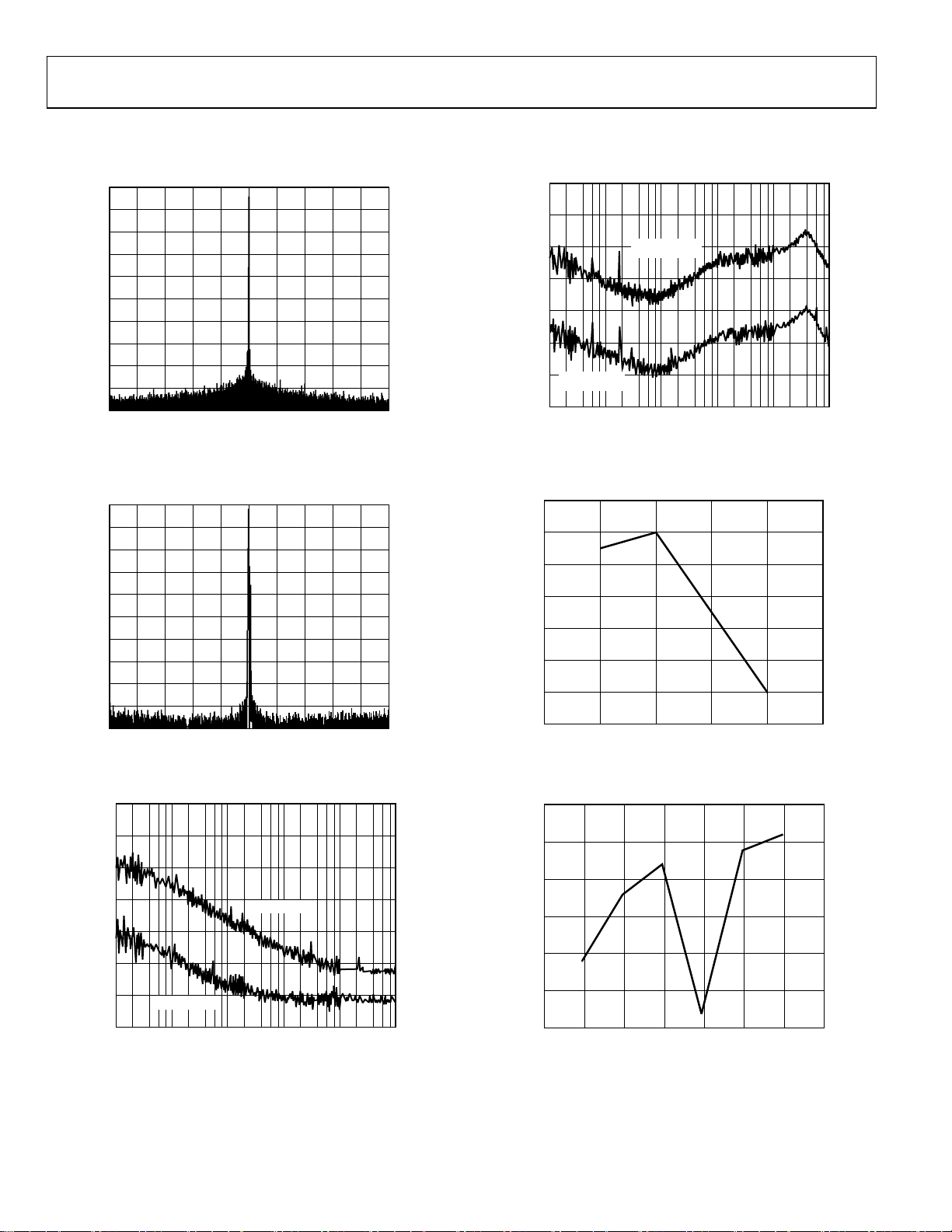
Figure 18 and Figure 19 show the residual phase noise performance of the AD9852 when operating with a 300 MHz reference clock with
the REFCLK multiplier bypassed vs. a 30 MHz reference clock with the REFCLK multiplier enabled at 10×.
0
–10
–20
–30
–40
–50
–60
–70
–80
–90
100
CENTER 112.469MHz
50kHz/ SPAN 500kHz
00634-016
Figure 16. A Slight Change in Tuning Word Yields Dramatically Better Results;
112.469 MHz with All Spurs Shifted Out-of-Band, 300 MHz REFCLK
–90
–100
–110
–120
–130
–140
PHASE NOISE (dBc/Hz)
–150
A
= 5MHz
OUT
–160
10 1M100 100k10k1k
30 MHz REFCLK with REFCLK Multiplier = 10×
A
= 80MHz
OUT
FREQUENCY (Hz)
Figure 19. Residual Phase Noise,
00634-019
0
–10
–20
–30
–40
–50
–60
–70
–80
–90
100
CENTER 39.1MHz
5kHz/ SPAN 50kHz
Figure 17. Narrow-Band SFDR, 39.1 MHz, 50 kHz BW,
200 MHz REFCLK with REFCLK Multiplier Bypassed
–100
–110
–120
–130
–140
–150
PHASE NOISE (dBc/Hz)
–160
–170
10 1M100 100k10k1k
A
OUT
= 5MHz
A
= 80MHz
OUT
FREQUENCY (Hz)
Figure 18. Residual Phase Noise,
300 MHz REFCLK with REFCLK Multiplier Bypassed
00634-017
00634-018
55
54
53
52
51
SFDR (dBc)
50
49
48
0
5 1015202
DAC CURRENT (mA)
Figure 20. SFDR vs. DAC Current, 59.1 A
OUT
5
00634-020
,
300 MHz REFCLK with REFCLK Multiplier Bypassed
620
615
610
605
600
SUPPLY CURRENT (mA)
595
590
20 40 60 80 100 120 140
0
FREQUENCY (MHz)
00634-021
Figure 21. Supply Current vs. Output Frequency (Variation Is Minimal,
Expressed as a Percentage, and Heavily Dependent on Tuning Word)
Rev. E | Page 14 of 52
AD9852
1200
1000
RISE TIME
1.04ns
JITTER
[10.6ps RMS]
–33ps 0ps +33ps
500ps/DIV 232mV/DIV 50Ω INPUT
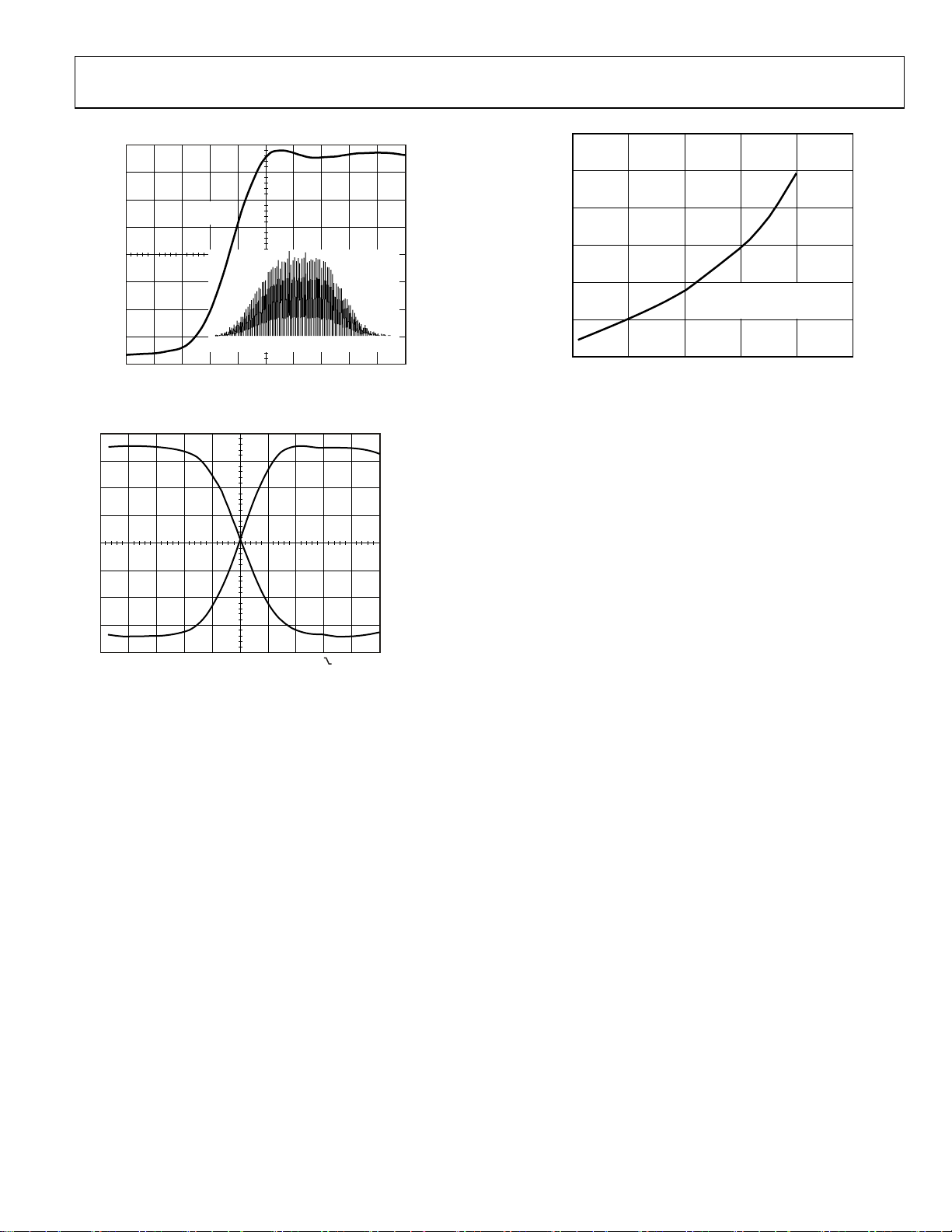
Figure 22. Typical Comparator Output Jitter, 40 MHz A
300 MHz REFCLK with REFCLK Multiplier Bypassed
00634-022
,
OUT
REF1 RISE
1.174ns
C1 FALL
1.286ns
800
600
400
AMPLITUDE (mV p-p)
200
0
0
100 200 300 400 500
MINIMUM COMPARATOR
INPUT DRIVE
= 0.5V
V
CM
FREQUENCY (MHz)
00634-024
Figure 24. Comparator Toggle Voltage Requirement
CH1 500mVΩ M 500ps CH1
Figure 23. Comparator Rise/Fall Times
980mV
00634-023
Rev. E | Page 15 of 52
AD9852
TYPICAL APPLICATIONS
RF/IF
INPUT
BASEBAND
REFCLK
AD9852
LOW-PASS
FILTER
COS
00634-025
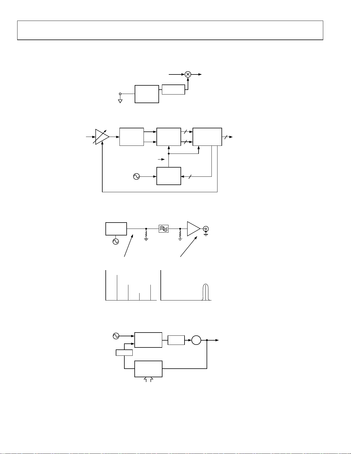
Figure 25. Synthesized LO Application for the AD9852
8
8
ADC ENCODE
48
CHIP/SYMBOL/PN
RATE DATA
DIGITAL
DEMODULATOR
AGC
Rx BASEBAND
DIGITAL
DATA OUT
00634-026
RF IN
Rx
VCA
I/Q MIXER
AND
LOW-PASS
FILTER
ADC CLOCK FREQUENCY
LOCKED TO Tx CHIP/
SYMBOL/PN RATE
REFERENCE
CLOCK
I
Q
DUAL
8-/10-BIT
ADC
AD9852
CLOCK
GENERATOR
Figure 26. Chip Rate Generator in Spread Spectrum Application
AD9852
I
OUT
50Ω
BAND-PASS
FILTER
AMPLIFIER
50Ω
AD9852
SPECTRUM
FUNDAMENTAL
F
C
IMAGE
– F
+ F
F
O
C
IMAGE
F
CLK
O
FINAL OUTPUT
SPECTRUM
FC + F
IMAGE
O
BAND-PASS
FILTER
00634-027
Figure 27. Using an Aliased Image to Generate a High Frequency
REFERENCE
CLOCK
LOOP
FILTER
REFCLK IN
PROGRAMMABLE
DIVIDE-BY-N FUNCTION
(WHERE N = 2
FILTER
DAC OUT
PHASE
COMPARATOR
AD9852
DDS
TUNING
WORD
Figure 28. Programmable Fractional Divide-by-N Synthesizer
RF FREQUENCY
VCO
48
/TUNING WORD)
OUT
00634-028
Rev. E | Page 16 of 52
 Loading...