Analog Devices AD9852 Datasheet
REV. 0
Information furnished by Analog Devices is believed to be accurate and
reliable. However, no responsibility is assumed by Analog Devices for its
use, nor for any infringements of patents or other rights of third parties
which may result from its use. No license is granted by implication or
otherwise under any patent or patent rights of Analog Devices.
a
AD9852
One Technology Way, P.O. Box 9106, Norwood, MA 02062-9106, U.S.A.
Tel: 781/329-4700 World Wide Web Site: http://www.analog.com
Fax: 781/326-8703 © Analog Devices, Inc., 1999
CMOS 300 MHz
Complete-DDS
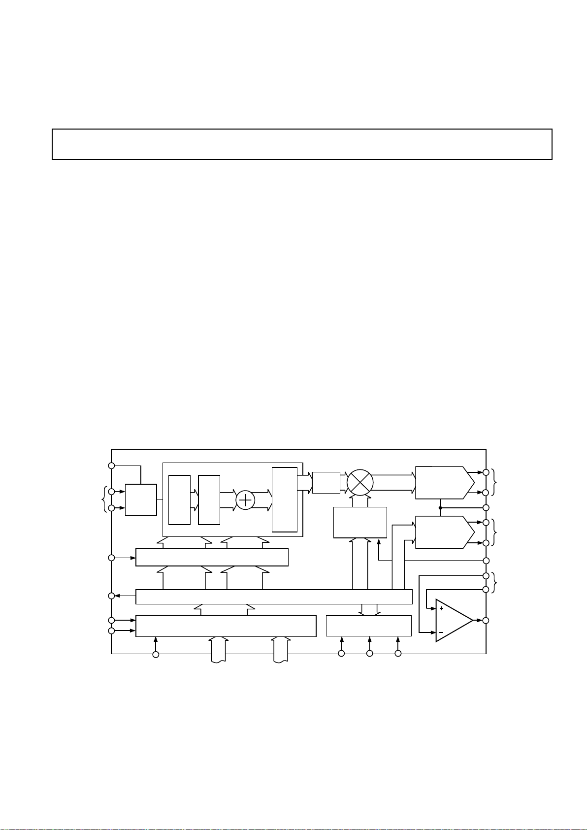
FUNCTIONAL BLOCK DIAGRAM
PHASE/OFFSET
MODULATION
INV.
SINC
FILTER
SINE-TO-AMPLITUDE
CONVERTER
PHASE
ACCUMULATOR
FREQUENCY
ACCUMULATOR
14-BIT PHASE
OFFSET/
MODULATION
48-BIT
FREQUENCY
TUNING WORD
FREQUENCY TUNING WORD/PHASE WORD
MULTIPLEXER AND RAMP START STOP LOGIC
RAMP-UP/-DOWN
CLOCK/LOGIC
AND
MULTIPLEXER
12-BIT
DATA
PROGRAMMABLE RATE
AND UPDATE CLOCKS
12
12
12
COMPARATOR
AMPLITUDE
MODULATION
DATA
12-BIT CONTROL
DAC
PROGRAMMING REGISTERS
43–203
REF CLK
MULTI-
PLEXER
AD9852
DIFF/SINGLE
SELECT
REFERENCE
CLOCK IN
FSK/BPSK/HOLD
DATA IN
BIDIRECTIONAL
I/O UPDATE
READ
WRITE
SERIAL/PARALLEL
SELECT
6-BIT ADDRESS
OR SERIAL
PROGRAMMING
LINES
8-BIT PARALLEL
LOAD
MASTER
RESET
+V
S
GND
CLOCK OUT
ANALOG IN
SHAPED
ON/OFF KEYING
ANALOG OUT
DAC R
SET
ANALOG OUT
300MHz DDS
I
Q
DIGITAL
MULTIPLIER
12-BIT DDS
DAC
I/O PORT BUFFERS
FEATURES
300 MHz Internal Clock Rate
Integrated 12-Bit Output DACs
Ultrahigh-Speed, 3 ps RMS Jitter Comparator
Excellent Dynamic Performance: 80 dB SFDR @ 100 MHz
(ⴞ1 MHz) A
OUT
4ⴛ to 20ⴛ Programmable Reference Clock Multiplier
Dual 48-Bit Programmable Frequency Registers
Dual 14-Bit Programmable Phase Offset Registers
12-Bit Amplitude Modulation and Programmable
Shaped On/Off Keying Function
Single Pin FSK and PSK Data Interface
Linear or Nonlinear FM Chirp Functions with Single
Pin Frequency “Hold” Function
Frequency-Ramped FSK
<25 ps RMS Total Jitter in Clock Generator Mode
Automatic Bidirectional Frequency Sweeping
SIN(x)/x Correction
Simplified Control Interface
10 MHz Serial, 2-Wire or 3-Wire SPI-Compatible or
100 MHz Parallel 8-Bit Programming
3.3 V Single Supply
Multiple Power-Down Functions
Single-Ended or Differential Input Reference Clock
Small 80-Lead LQFP Packaging
APPLICATIONS
Agile, L.O. Frequency Synthesis
Programmable Clock Generator
FM Chirp Source for Radar and Scanning Systems
Test and Measurement Equipment
Commercial and Amateur RF Exciter
GENERAL DESCRIPTION
The AD9852 digital synthesizer is a highly integrated device
that uses advanced DDS technology, coupled with an internal
high-speed, high-performance D/A converters and a comparator
to form a digitally-programmable agile synthesizer function. When
referenced to an accurate clock source, the AD9852 generates a
highly stable, frequency-phase amplitude-programmable sine
wave output that can be used as an agile L.O. in communications,
radar, and many other applications. The AD9852’s innovative
high-speed DDS core provides 48-bit frequency resolution
(1 microHertz tuning steps). Phase truncation to 17 bits assures
excellent SFDR. The AD9852’s circuit architecture allows the
(continued on page 13)

–2–
REV. 0
AD9852–SPECIFICATIONS
(VS = 3.3 V ⴞ 5%, R
SET
= 3.9 k⍀ external reference clock frequency = 30 MHz with
REFCLK Multiplier enabled at 10ⴛ for AD9852ASQ, external reference clock frequency = 20 MHz with REFCLK Multiplier enabled at 10ⴛ for
AD9852AST, unless otherwise noted.)
Test AD9852ASQ AD9852AST
Parameter Temp Level Min Typ Max Min Typ Max Unit
REF CLOCK INPUT CHARACTERISTICS
1
Internal Clock Frequency Range FULL VI 5 300 5 200 MHz
External REF Clock Frequency Range
REFCLK Multiplier Enabled FULL VI 5 75 5 50 MHz
REFCLK Multiplier Disabled FULL VI 5 300 5 200 MHz
Duty Cycle 25°C V 50 50 %
Input Capacitance 25°CIV 3 3 pF
Input Impedance 25°C IV 100 100 kΩ
Differential Mode Common-Mode Voltage Range
Minimum Signal Amplitude 25°C IV 800 800 mV p-p
Common-Mode Range 25°C IV 1.6 1.75 1.9 1.6 1.75 1.9 V
V
IH
(Single-Ended Mode) 25°C IV 2.3 2.3 V
V
IL
(Single-Ended Mode) 25°CIV 1 1 V
DAC STATIC OUTPUT CHARACTERISTICS
Output Update Speed FULL I 300 200 MSPS
Resolution 25°C IV 12 12 Bits
Sine and Aux. DAC Full-Scale Output Current 25°C IV 5 10 20 5 10 20 mA
Gain Error 25°C I –6 +2.25 –6 +2.25 % FS
Output Offset 25°CI 2 2 µA
Differential Nonlinearity 25°C I 0.3 1.25 0.3 1.25 LSB
Integral Nonlinearity 25°C I 0.6 1.66 1 1.66 LSB
Output Impedance 25°C I 100 100 kΩ
Voltage Compliance Range 25°C I –0.5 +1.0 –0.5 +1.0 V
DAC WIDEBAND SFDR
1 MHz to 20 MHz A
OUT
25°C V 58 58 dBc
20 MHz to 40 MHz A
OUT
25°C V 56 56 dBc
40 MHz to 60 MHz A
OUT
25°C V 52 52 dBc
60 MHz to 80 MHz A
OUT
25°C V 48 48 dBc
80 MHz to 100 MHz A
OUT
25°C V 48 48 dBc
100 MHz to 120 MHz A
OUT
25°C V 50 dBc
DAC NARROWBAND SFDR
10 MHz A
OUT
(±1 MHz) 25°C V 83 83 dBc
10 MHz A
OUT
(±250 kHz) 25°C V 83 83 dBc
10 MHz A
OUT
(±50 kHz) 25°C V 91 91 dBc
41 MHz A
OUT
(±1 MHz) 25°C V 82 82 dBc
41 MHz A
OUT
(±250 kHz) 25°C V 84 84 dBc
41 MHz A
OUT
(±50 kHz) 25°C V 89 89 dBc
119 MHz A
OUT
(±1 MHz) 25°C V 71 71 dBc
119 MHz A
OUT
(±250 kHz) 25°C V 77 77 dBc
119 MHz A
OUT
(±50 kHz) 25°C V 83 83 dBc
RESIDUAL PHASE NOISE
(A
OUT
= 5 MHz, Ext. CLK = 30 MHz,
REFCLK Multiplier Engaged at 10×)
1 kHz Offset 25°C V 140 140 dBc/Hz
10 kHz Offset 25°C V 138 138 dBc/Hz
100 kHz Offset 25°C V 142 142 dBc/Hz
(A
OUT
= 5 MHz, Ext. CLK = 300 MHz,
REFCLK Multiplier Bypassed)
1 kHz Offset 25°C V 142 142 dBc/Hz
10 kHz Offset 25°C V 148 148 dBc/Hz
100 kHz Offset 25°C V 152 152 dBc/Hz
PIPELINE DELAYS
Phase Accumulator and DDS Core 25°C IV 17 17 SysClk Cycles
Inverse Sinc Filter 25°C IV 12 12 SysClk Cycles
Digital Multiplier 25°C IV 10 10 SysClk Cycles

–3–
REV. 0
AD9852
Test AD9852ASQ AD9852AST
Parameter Temp Level Min Typ Max Min Typ Max Unit
MASTER RESET DURATION 25°C IV 10 10 SysClk Cycles
COMPARATOR INPUT CHARACTERISTICS
Input Capacitance 25°CV 3 3 pF
Input Resistance 25°C IV 500 500 ±1kΩ
Input Current 25°CI ±1 ±5 ±1 ±5 µA
Hysteresis 25°C IV 10 20 10 20 mV p-p
COMPARATOR OUTPUT CHARACTERISTICS
Logic “1” Voltage, High Z Load FULL VI 3.10 3.10 V
Logic “0” Voltage, High Z Load FULL VI 0.16 0.16 V
Output Power, 50 Ω Load, 120 MHz Toggle Rate 25°C I 9 11 9 11 dBm
Propagation Delay 25°CIV 3 3 ns
Output Duty Cycle Error
2
25°CI –10 ±1 +10 –10 ±1 +10 %
Rise/Fall Time, 5 pF Load 25°CV 2 2 ns
Toggle Rate, High Z Load 25°C IV 300 350 300 350 MHz
Toggle Rate, 50 Ω Load 25°C IV 375 400 375 400 MHz
Output Cycle-to-Cycle Jitter
3
25°C IV 3 3 ps rms
COMPARATOR NARROWBAND SFDR
4
10 MHz (±1 MHz) 25°C V 84 84 dBc
10 MHz (±250 kHz) 25°C V 84 84 dBc
10 MHz (±50 kHz) 25°C V 92 92 dBc
41 MHz (±1 MHz) 25°C V 76 76 dBc
41 MHz (±250 kHz) 25°C V 82 82 dBc
41 MHz (±50 kHz) 25°C V 89 89 dBc
119 MHz (±1 MHz) 25°C V 73 73 dBc
119 MHz (±250 kHz) 25°C V 73 73 dBc
119 MHz (±50 kHz) 25°C V 83 83 dBc
CLOCK GENERATOR OUTPUT JITTER
4
5 MHz A
OUT
25°C V 23 23 ps rms
40 MHz A
OUT
25°C V 12 12 ps rms
100 MHz A
OUT
25°C V 7 7 ps rms
PARALLEL I/O TIMING CHARACTERISTICS
T
ASU
(Address Setup Time to WR Signal Active) FULL IV 4 4 ns
T
ADHW
(Address Hold Time to WR Signal Inactive) FULL IV 3 3 ns
T
DSU
(Data Setup Time to WR Signal Inactive) FULL IV 2 2 ns
T
DHD
(Data Hold Time to WR Signal Inactive) FULL IV 0 0 ns
T
WRLOW
(WR Signal Minimum Low Time) FULL IV 3 3 ns
T
WRHIGH
(WR Signal Minimum High Time) FULL IV 7 7 ns
TWR (WR Signal Minimum Period) FULL IV 10 10 ns
T
ADV
(Address to Data Valid Time) FULL V 15 15 15 15 ns
T
ADHR
(Address Hold Time to RD Signal Inactive) FULL IV 5 5 ns
T
RDLOV
(RD Low-to-Output Valid) FULL IV 15 15 ns
T
RDHOZ
(RD High-to-Data Three-State) FULL IV 10 10 ns
SERIAL I/O TIMING CHARACTERISTICS
T
PRE
(CS Setup Time) FULL IV 30 30 ns
T
SCLK
(Period of Serial Data Clock) FULL IV 100 100 ns
T
DSU
(Serial Data Setup Time) FULL IV 30 30 ns
T
SCLKPWH
(Serial Data Clock Pulsewidth High) FULL IV 40 40 ns
T
SCLKPWL
(Serial Data Clock Pulsewidth Low) FULL IV 40 40 ns
T
DHLD
(Serial Data Hold Time) FULL IV 0 0 ns
TDV (Data Valid Time) FULL V 30 30 ns
CMOS LOGIC INPUTS
Logic “1” Voltage 25°C I 2.7 2.7 V
Logic “0” Voltage 25°C I 0.4 0.4 V
Logic “1” Current 25°CIV ±5 ±5 µA
Logic “0” Current 25°CIV ±5 ±5 µA
Input Capacitance 25°CV 3 3 pF

–4–
REV. 0
AD9852–SPECIFICATIONS
CAUTION
ESD (electrostatic discharge) sensitive device. Electrostatic charges as high as 4000 V readily
accumulate on the human body and test equipment and can discharge without detection. Although
the AD9852 features proprietary ESD protection circuitry, permanent damage may occur on
devices subjected to high energy electrostatic discharges. Therefore, proper ESD precautions are
recommended to avoid performance degradation or loss of functionality.
WARNING!
ESD SENSITIVE DEVICE
Test AD9852ASQ AD9852AST
Parameter Temp Level Min Typ Max Min Typ Max Unit
POWER SUPPLY
5
+VS Current
6
25°C I 815 922 585 660 mA
+VS Current
7
25°C I 640 725 465 520 mA
+VS Current
8
25°C I 585 660 425 475 mA
P
DISS
6
25°C I 2.7 3.195 1.93 2.385 W
P
DISS
7
25°C I 2.115 2.515 1.53 1.805 W
P
DISS
8
25°C I 1.930 2.285 1.400 1.650 W
P
DISS
Power-Down Mode 25°C I 50 50 mW
NOTES
1
The reference clock inputs are configured to accept a 1 V p-p (minimum) dc offset sine wave centered at one-half the applied V
DD
or a 3 V TTL-level pulse input.
2
Change in duty cycle from 1 MHz to 100 MHz with 1 V p-p sine wave input and 0.5 V threshold.
3
Represents comparator’s inherent cycle-to-cycle jitter contribution. Input signal is a 1 V, 40 MHz square wave. Measurement device Wavecrest DTS – 2075.
4
Comparator input originates from Analog Out section via external 7-pole elliptic LPF. Single-ended input, 0.5 V p-p. Comparator output terminated in 50 Ω.
5
Important: In the 80-lead LQFP package simultaneous operation at the maximum ambient temperature of 85°C and at the maximum internal clock frequency at
200 MHz may cause the maximum die junction temperature of 150°C to be exceeded. Refer to the section of the data sheet entitled Power Dissipation section and
Thermal Considerations section for derating and thermal management information.
6
All functions engaged.
7
All functions except inverse sinc engaged.
8
All functions except inverse sinc and digital multipliers engaged.
Specifications subject to change without notice.
EXPLANATION OF TEST LEVELS
Test Level
I – 100% Production Tested.
III – Sample Tested Only.
IV – Parameter is guaranteed by design and characterization
testing.
V – Parameter is a typical value only.
VI – Devices are 100% production tested at 25°C and
guaranteed by design and characterization testing
for industrial operating temperature range.
ABSOLUTE MAXIMUM RATINGS*
Maximum Junction Temperature . . . . . . . . . . . . . . . . 150°C
V
S
. . . . . . . . . . . . . . . . . . . . . . . . . . . . . . . . . . . . . . . . . . . 4 V
Digital Inputs . . . . . . . . . . . . . . . . . . . . . . . . . –0.7 V to +V
S
Digital Output Current . . . . . . . . . . . . . . . . . . . . . . . . . 5 mA
Storage Temperature . . . . . . . . . . . . . . . . . . –65°C to +150°C
Operating Temperature . . . . . . . . . . . . . . . . . –40°C to +85°C
Lead Temperature (Soldering 10 sec) . . . . . . . . . . . . . 300°C
Maximum Clock Frequency . . . . . . . . . . . . . . . . . . 300 MHz
*Absolute maximum ratings are limiting values, to be applied individually, and
beyond which the serviceability of the circuit may be impaired. Functional
operability under any of these conditions is not necessarily implied. Exposure of
absolute maximum rating conditions for extended periods of time may affect device
reliability.
ORDERING GUIDE
Model Temperature Range Package Description Package Option
AD9852ASQ –40°C to +85°C Thermally-Enhanced 80-Lead LQFP SQ-80
AD9852AST –40°C to +85°C 80-Lead LQFP ST-80
AD9852/PCB 0°C to 70°C Evaluation Board

AD9852
–5–
REV. 0
PIN FUNCTION DESCRIPTIONS
Pin
No. Pin Name Function
1–8 D7–D0 Eight-Bit Bidirectional Parallel Programming Data Inputs. Used only in parallel programming mode.
9, 10, 23, DVDD Connections for the Digital Circuitry Supply Voltage. Nominally 3.3 V more positive than AGND
24, 25, 73, and DGND.
74, 79, 80
11, 12, 26, DGND Connections for Digital Circuitry Ground Return. Same potential as AGND.
27, 28, 72,
75, 76, 77,
78
13, 35, 57 NC No Internal Connection.
58, 63
14–19 A5–A0 Six-Bit Parallel Address Inputs for Program Registers. Used only in parallel programming mode. A0, A1,
and A2 have a second function when the serial programming mode is selected. See immediately below.
(17) A2/IO RESET Allows a RESET of the serial communications bus that is unresponsive due to improper program-
ming protocol. Resetting the serial bus in this manner does not affect previous programming nor
does it invoke the “default” programming values seen in the Table V. Active HIGH.
(18) A1/SDO Unidirectional Serial Data Output for Use in 3-Wire Serial Communication Mode.
(19) A0/SDIO Bidirectional Serial Data Input/Output for Use in 2-Wire Serial Communication Mode.
20 I/O UD Bidirectional Frequency Update Signal. Direction is selected in control register. If selected as an input,
a rising edge will transfer the contents of the programming registers to the internal works of the IC for
processing. If I/O UD is selected as an output, an output pulse (low to high) of eight system clock cycle
duration indicates that an internal frequency update has occurred.
21 WRB/SCLK Write Parallel Data to Programming Registers. Shared function with SCLK. Serial clock signal
associated with the serial programming bus. Data is registered on the rising edge. This pin is shared with
WRB when the parallel mode is selected.
22 RDB/CSB Read Parallel Data from Programming Registers. Shared function with CSB. Chip-select signal
associated with the serial programming bus. Active LOW. This pin is shared with RDB when
the parallel mode is selected.
29 FSK/BPSK/ Multifunction Pin According to the Mode of Operation Selected in the Programming Control Register.
HOLD If in the FSK mode logic low selects F1, logic high selects F2. If in the BPSK mode, logic low selects
Phase 1, logic high selects Phase 2. If in the Chirp mode, logic high engages the HOLD function
causing the frequency accumulator to halt at its current location. To resume or commence Chirp,
logic low is asserted.
30 SHAPED Must First Be Selected in the Programming Control Register to Function. A logic high will cause the
KEYING cosine DAC output to ramp-up from zero-scale to full-scale amplitude at a preprogrammed rate.
Logic low causes the full-scale output to ramp-down to zero-scale at the preprogrammed rate.
31, 32, 37 AVDD Connections for the Analog Circuitry Supply Voltage. Nominally 3.3 V more positive than AGND
38, 44, 50, and DGND.
54, 60, 65
33, 34, 39, AGND Connections for Analog Circuitry Ground Return. Same potential as DGND.
40, 41, 45,
46, 47, 53,
59, 62, 66,
67
36 VOUT Internal High-Speed Comparator’s Noninverted Output Pin. Designed to drive 10 dBm to 50 Ω load
as well as standard CMOS logic levels.
42 VINP Voltage Input Positive. The internal high-speed comparator’s noninverting input.
43 VINN Voltage Input Negative. The internal high-speed comparator’s inverting input.
48 IOUT1 Unipolar Current Output of the Cosine DAC.
49 IOUT1B Complementary Unipolar Current Output of the Cosine DAC.
51 IOUT2B Complementary Unipolar Current Output of the Auxiliary DAC.
52 IOUT2 Unipolar Current Output of the Auxiliary DAC.

AD9852
–6–
REV. 0
Pin
No. Pin Name Function
55 DACBP Common Bypass Capacitor Connection for Both DACs. A 0.01 µF chip cap from this pin to AVDD
improves harmonic distortion and SFDR slightly. No connect is permissible (slight SFDR degradation).
56 DAC R
SET
Common Connection for Both DACs to Set the Full-Scale Output Current. R
SET
= 39.9/I
OUT
.
Normal R
SET
range
is from 8 kΩ (5 mA) to 2 kΩ (20 mA).
61 PLL FILTER This pin provides the connection for the external zero compensation network of the REFCLK
Multiplier’s PLL loop filter. The zero compensation network consists of a 1.3 kΩ resistor in series
with a 0.01 µF capacitor. The other side of the network should be connected to AVDD as close as
possible to Pin 60. For optimum phase noise performance, the REFCLK Multiplier can be bypassed
by setting the “Bypass PLL” bit in control register 1E.
64 DIFF CLK Differential REFCLK Enable. A high level of this pin enables the differential clock inputs, REFCLK
and REFCLKB ENABLE (Pins 69 and 68 respectively). The minimum differential signal amplitude
required is 800 mV p-p. The centerpoint or common-mode range of the differential signal ranges
from 1.6 V to 1.9 V.
68 REFCLKB The Complementary (180 Degrees Out-of-Phase) Differential Clock Signal. User should tie this pin
high or low when single-ended clock mode is selected. Same signal levels as REFCLK.
69 REFCLK Single-Ended Reference Clock Input or One of Two Differential Clock Signals. Normal 3.3 V CMOS
logic levels or 1 V p-p sine wave centered about 1.6 V.
70 S/P SELECT Selects Between Serial Programming Mode (Logic LOW) and Parallel Programming Mode
(Logic High).
71 MASTER Initializes the serial/parallel programming bus to prepare for user programming; sets programming
RESET registers to a “do-nothing” state defined by the default values seen in the Table V. Active on logic
high. Asserting MASTER RESET is essential for proper operation upon power-up.
AD9852
–7–
REV. 0
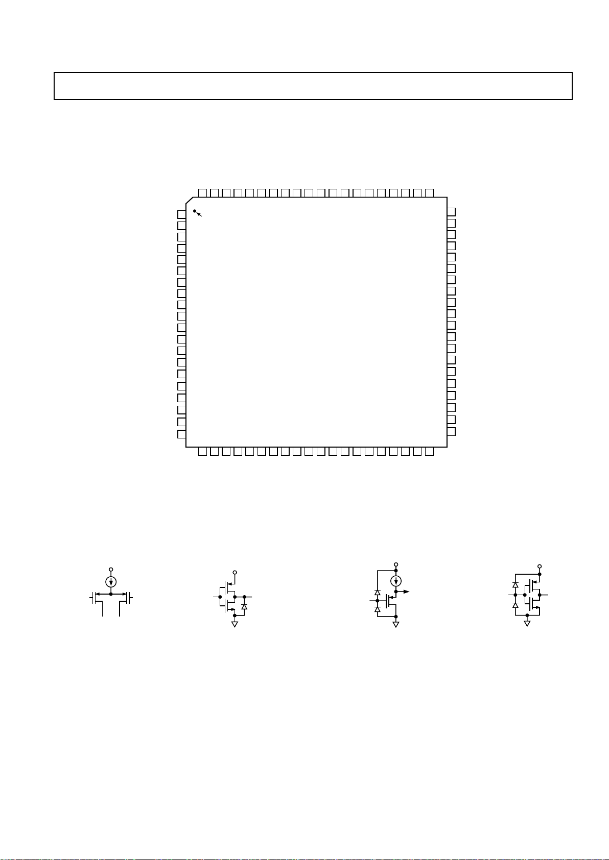
PIN CONFIGURATION
PIN 1
IDENTIFIER
TOP VIEW
(Not to Scale)
AD9852
80-PIN LQFP 14 3 14 3 1.4
60
59
58
57
56
55
54
53
52
51
50
49
48
47
46
45
44
43
42
40
20
19
18
17
16
15
14
13
12
11
10
9
8
7
6
5
4
3
2
1
80 79 78 77 76 75 74 73 72 71 70 69 68 67 66 65 64 63 62 61
21 22 23 24 25 26 27 28 29 30 31 32 33 34 35 36 37 38 39 40
D7
D6
D5
D4
D3
D2
D1
D0
DVDD
DVDD
DGND
DGND
NC
A5
A4
A3
A2/IO RESET
A1/SDO
A0/SDIO
I/O UD
WRB/SCLK
RDB/CSB
DVDD
DVDD
DVDD
DGND
DGND
DGND
FSK/BPSK/HOLD
SHAPED KEYING
AVDD
AVDD
AGND
AGND
NC
VOUT
AVDD
AVDD
AGND
AGND
AGND
VINP
VINN
AVDD
AGND
AGND
AGND
IOUT1
IOUT1B
AVDD
IOUT2B
IOUT2
AGND
AVDD
DACBP
DAC R
SET
NC
NC
AGND
AVDD
PLL FILTER
AGND
NC
DIFF CLK ENABLE
AVDD
AGND
AGND
REFCLOCKB
REFCLOCK
S/P SELECT
MASTER RESET
DGND
DVDD
DVDD
DGND
DGND
DGND
DGND
DVDD
DVDD
NC = NO CONNECT
Figure 1. Equivalent Input and Output Circuits
a. DAC Outputs b. Comparator Output c. Comparator Input d. Digital Input
V
DD
I
OUTIOUTB
V
DD
VINP/
VINN
V
DD
DIGITAL
IN
DIGITAL
OUT
V
DD
AD9852
–8–
REV. 0
0
START 0Hz
–10
–20
–30
–40
–50
–60
–70
–80
–90
–100
15MHz/ STOP 150MHz
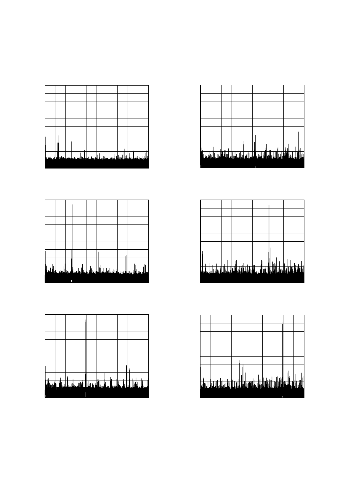
Figure 2. Wideband SFDR, 19.1 MHz
0
START 0Hz
–10
–20
–30
–40
–50
–60
–70
–80
–90
–100
15MHz/ STOP 150MHz
Figure 3. Wideband SFDR, 39.1 MHz
0
START 0Hz
–10
–20
–30
–40
–50
–60
–70
–80
–90
–100
15MHz/ STOP 150MHz
Figure 4. Wideband SFDR, 59.1 MHz
0
START 0Hz
–10
–20
–30
–40
–50
–60
–70
–80
–90
–100
15MHz/ STOP 150MHz
Figure 5. Wideband SFDR, 79.1 MHz
0
START 0Hz
–10
–20
–30
–40
–50
–60
–70
–80
–90
–100
15MHz/ STOP 150MHz
Figure 6. Wideband SFDR, 99.1 MHz
0
START 0Hz
–10
–20
–30
–40
–50
–60
–70
–80
–90
–100
15MHz/ STOP 150MHz
Figure 7. Wideband SFDR, 119.1 MHz
Figures 2–7 indicate the wideband harmonic distortion Performance of the AD9852 from 19.1 MHz to 119.1 MHz Fundamental Output, Reference Clock = 30 MHz, REFCLK Multiplier = 10. Each graph plotted from 0 MHz to 150 MHz.
AD9852
–9–
REV. 0
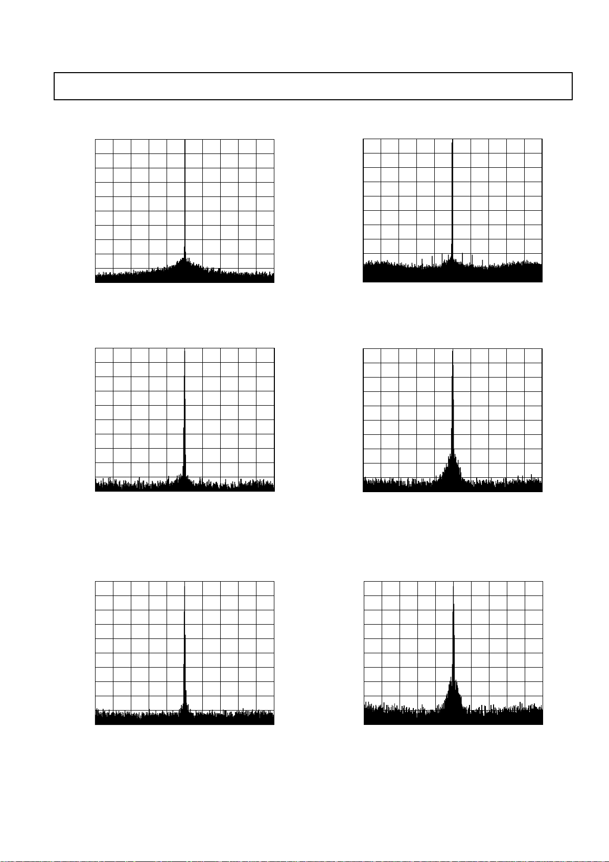
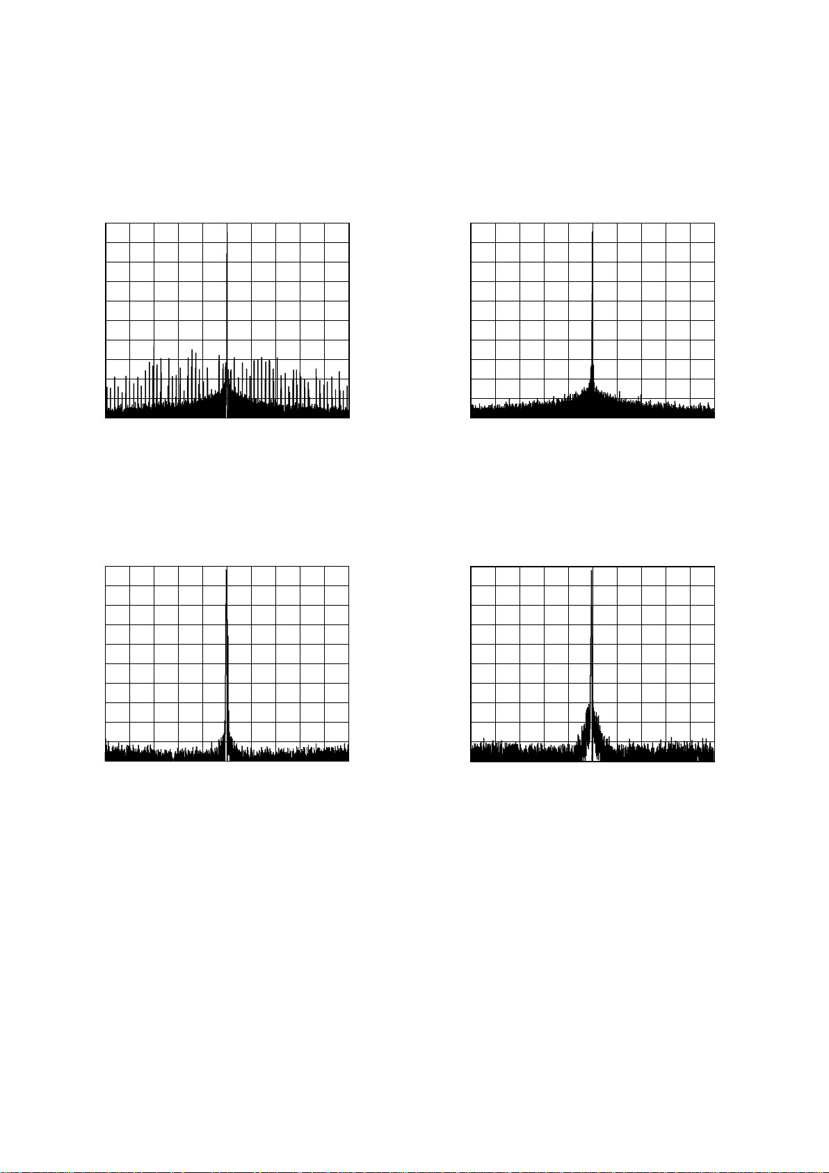
Figures 8–11 show the tradeoff in elevated noise floor, increased phase noise, and occasional discrete spurious energy when the
internal REFCLK Multiplier circuit is engaged. Plots with wide (1 MHz) and narrow (50 kHz) spans are shown.
0
CENTER 39.1MHz
–10
–20
–30
–40
–50
–60
–70
–80
–90
–100
100kHz/ SPAN 1MHz
Figure 10. Narrowband SFDR, 39.1 MHz, 1 MHz BW,
30 MHz EXTCLK with REFCLK Multiply = 10
×
0
CENTER 39.1MHz
–10
–20
–30
–40
–50
–60
–70
–80
–90
–100
5kHz/ SPAN 50kHz
Figure 11. Narrowband SFDR, 39.1 MHz, 50 kHz BW,
30 MHz EXTCLK/REFCLK Multiplier = 10
×
0
CENTER 39.1MHz
–10
–20
–30
–40
–50
–60
–70
–80
–90
–100
5kHz/ SPAN 50kHz
Figure 12. Narrowband SFDR, 39.1 MHz, 50 kHz BW,
100 MHz EXTCLK with REFCLK Multiplier Bypassed
0
CENTER 39.1MHz
–10
–20
–30
–40
–50
–60
–70
–80
–90
–100
100kHz/ SPAN 1MHz
Figure 8. Narrowband SFDR, 39.1 MHz, 1 MHz BW,
300 MHz EXTCLK with REFCLK Multiply Bypassed
0
CENTER 39.1MHz
–10
–20
–30
–40
–50
–60
–70
–80
–90
–100
5kHz/ SPAN 50kHz
Figure 9. Narrowband SFDR, 39.1 MHz, 50 kHz BW,
300 MHz EXTCLK with REFCLK Multiplier Bypassed
Figures 12 and 13 show the slight increase in noise floor both with and without the PLL when slower clock speeds are used to
generate the same fundamental frequency, that is, with a 100 MHz clock as opposed to a 300 MHz clock in Figures 9 and 11.
0
CENTER 39.1MHz
–10
–20
–30
–40
–50
–60
–70
–80
–90
–100
5kHz/ SPAN 50kHz
Figure 13. Narrowband SFDR, 39.1 MHz, 50 kHz BW,
10 MHz EXTCLK with REFCLK Multiplier = 10
×
AD9852
–10–
REV. 0
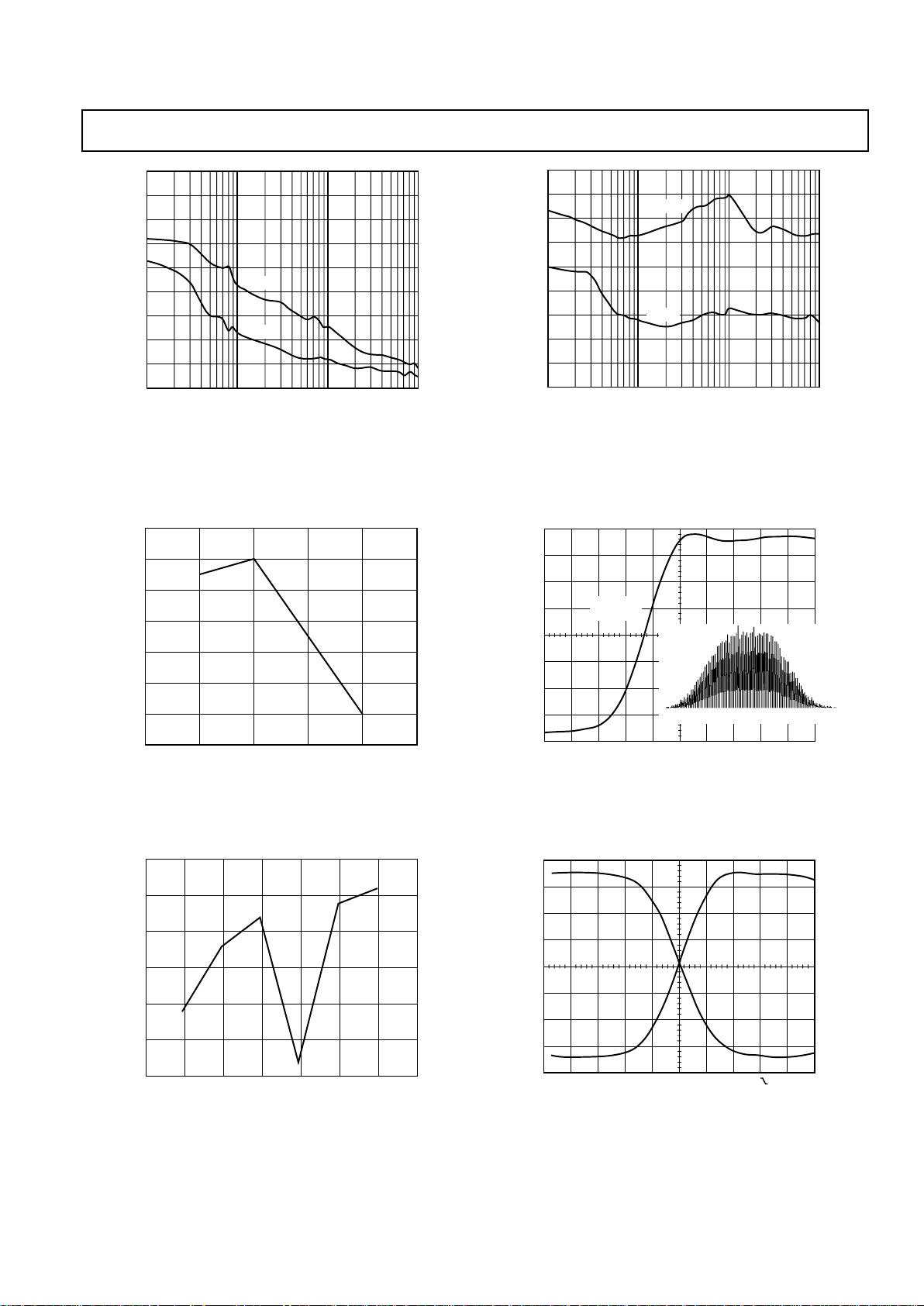
Figures 14 and 15 show the effects of utilizing “sweet spots” in the tuning range of a DDS. Figure 14 represents a tuning word that
accentuates the aberrations associated with truncation in the DDS algorithm. Figure 15 is essentially the same output frequency (a few
tuning codes over), but it displays much fewer spurs on the output due to the selection of a tuning “sweet spot.” Consideration
should be given to all DDS applications to exploit the benefit of sweet spot tuning.
0
CENTER 112.499MHz
–10
–20
–30
–40
–50
–60
–70
–80
–90
–100
50kHz/ SPAN 500kHz
Figure 14. T he Opposite of a “Sweet Spot.” 112.469 MHz
with multiple high energy spurs close around the
fundamental.
0
CENTER 112.469MHz
–10
–20
–30
–40
–50
–60
–70
–80
–90
–100
50kHz/ SPAN 500kHz
Figure 15. A slight change in tuning word yields
dramatically better results. 112.499 MHz with all
spurs shifted out-of-band.
Figures 16 and 17 show the narrowband performance of the AD9852 when operating with a 20 MHz reference clock and the
REFCLK Multiplier enabled at 10× vs. a 200 MHz external reference clock.
0
CENTER 39.1MHz
–10
–20
–30
–40
–50
–60
–70
–80
–90
–100
5kHz/ SPAN 50kHz
Figure 16. Narrowband SFDR, 39.1 MHz, 50 kHz BW,
200 MHz EXTCLK with REFCLK Multiplier Bypassed
0
CENTER 39.1MHz
–10
–20
–30
–40
–50
–60
–70
–80
–90
–100
5kHz/ SPAN 50kHz
Figure 17. Narrowband SFDR, 39.1 MHz, 50 kHz BW,
10 MHz EXTCLK with REFCLK Multiplier = 10
×
AD9852
–11–
REV. 0
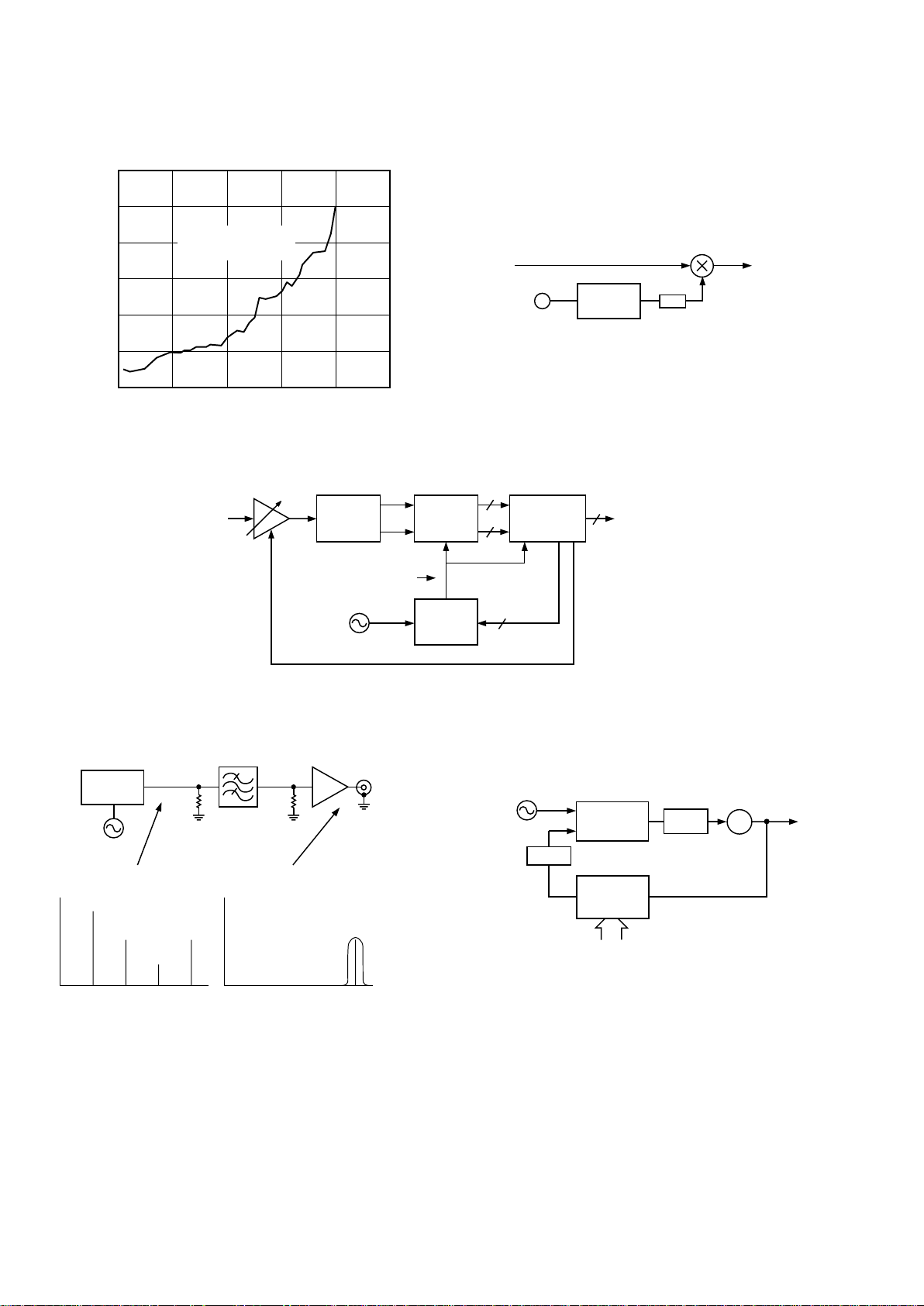
DAC CURRENT – mA
55
0
SFDR – dBc
54
53
52
51
50
49
48
510152025
Figure 19. SFDR vs. DAC Current, 59.1 MHz A
OUT
, 300 MHz
EXTCLK
FREQUENCY – MHz
620
0
SUPPLY CURRENT – mA
615
610
605
600
595
590
20 40 60 80 100 120 140
Figure 20. Supply Current vs. Output Frequency; Variation
Is Minimal as a Percentage and Heavily Dependent on
Tuning Word
FREQUENCY – Hz
–110
100
PHASE NOISE – dBc/Hz
–115
–120
–125
–130
–135
–140
–145
–150
–155
1k 10k 100k
80MHz
5MHz
a. Residual Phase Noise 300 MHz Direct Clocking
FREQUENCY – Hz
–110
100
PHASE NOISE – dBc/Hz
–115
–120
–125
–130
–135
–140
–145
–150
–155
1k 10k 100k
80MHz
5MHz
b. Residual Phase Noise, 300 MHz (10× REFCLK Multiplier
Enabled)
Figure 18. Residual Phase Noise, EXTCLK = 300 MHz, REFCLK Multiplier Disabled/Enabled at 10
×
RISE TIME
1.04ns
500ps/DIV 232mV/DIV 50V INPUT
JITTER
[10.6ps RMS]
–33ps 0ps +33ps
Figure 21. Typical Comparator Output Jitter, 40 MHz
A
OUT
, 300 MHz EXTCLK/REFCLK Multiplier Disabled
REF1 RISE
1.174ns
C1 FALL
1.286ns
CH1 500mVV M 500ps CH1
980mV
Figure 22. Comparator Rise/Fall Times
AD9852
–12–
REV. 0
FREQUENCY – MHz
1200
0
AMPLITUDE – mV p-p
1000
800
600
400
200
0
100 200 300 400 500
MINIMUM COMPARATOR
INPUT DRIVE
VCM = 0.5V
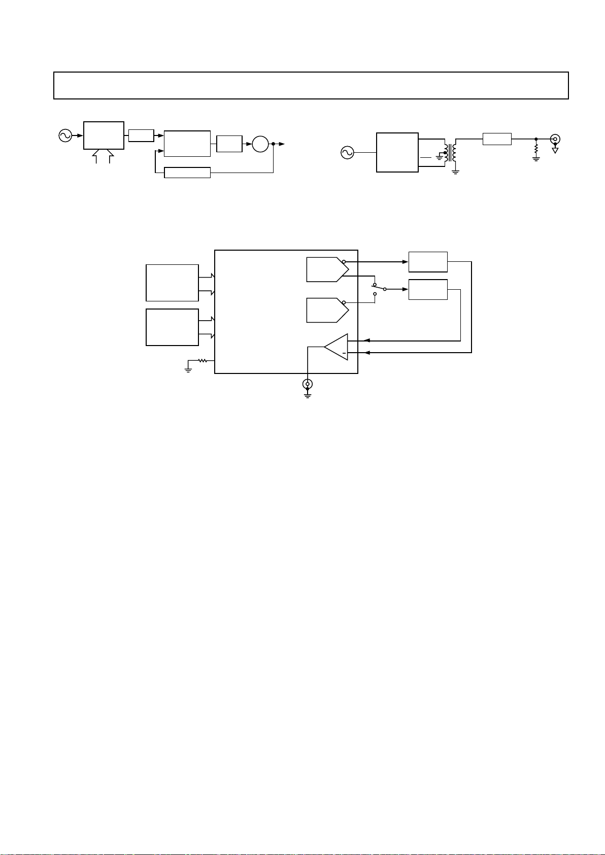
Figure 23. Comparator Toggle Voltage Requirement
I
Q
Rx
RF IN
DUAL
8-/10-BIT
ADC
DIGITAL
DEMODULATOR
Rx BASEBAND
DIGITAL DATA
OUT
8
8
I/Q MIXER
AND
LOW-PASS
FILTER
VCA
ADC ENCODE
ADC CLOCK FREQUENCY
LOCKED TO Tx CHIP/
SYMBOL/PN RATE
REFERENCE
CLOCK
48
CHIP/SYMBOL/PN
RATE DATA
AD9852
CLOCK
GENERATOR
Figure 25. Chip Rate Generator in Spread Spectrum Application
50V
BANDPASS
FILTER
50V
I
OUT
AD9852
FUNDAMENTAL
F
C
– F
O
IMAGE
F
CLK
FC + F
O
IMAGE
BANDPASS
FILTER
F
C
+ F
O
IMAGE
AD9852
SPECTRUM
FINAL OUTPUT
SPECTRUM
Figure 26. Using an Aliased Image to Generate a High
Frequency
VCO
LOOP
FILTER
PHASE
COMPARATOR
REFERENCE
CLOCK
FILTER
AD9852
DDS
TUNING
WORD
REF CLK IN
RF
FREQUENCY
OUT
DAC OUT
Figure 27. Programmable “Divide-by-N” Synthesizer
LPF
REFCLK
RF/IF
INPUT
AD9852
BASEBAND
SIN
Figure 24. Synthesized L.O. Application for the AD9852
AD9852
–13–
REV. 0
TUNING
WORD
VCO
LOOP
FILTER
PHASE
COMPARATOR
REF
CLOCK
RF
FREQUENCY
OUT
FILTER
AD9852
DDS
DIVIDE-BY-N
Figure 28. Agile High-Frequency Synthesizer
mPROCESSOR/
CONTROLLER
FPGA, ETC.
R
SET
8-BIT PARALLEL OR
SERIAL PROGRAMMING
DATA AND CONTROL
SIGNALS
AD9852
CMOS LOGIC "CLOCK" OUT
REFERENCE
CLOCK
300MHz MAX DIRECT
MODE OR 15 TO 75MHz
MAX IN THE 43-203 CLOCK
MULTIPLIER MODE
2kV
CONTROL
"I" DAC
1
2
NOTES:
I
OUT
= APPROX 20mA MAX WHEN R
SET
= 2kV
SWITCH POSTION 1 PROVIDES COMPLEMENTARY SINUSOIDAL SIGNALS TO THE COMPARATOR
TO PRODUCE A FIXED 50% OUTPUT DUTY CYCLE FROM THE COMPARATOR.
SWITCH POSTION 2 PROVIDES A USER PROGRAMMABLE DC THRESHOLD VOLTAGE TO ALLOW
SETTING OF THE COMPARATOR OUTPUT DUTY CYCLE.
LOW-PASS
FILTER
LOW-PASS
FILTER
+
Figure 30. Frequency Agile Clock Generator Applications for the AD9852
(continued from page 1)
generation of a sine output at frequencies up to 150 MHz, which
can be digitally tuned at a rate of up to 100 million new frequencies
per second. The (externally filtered) sine wave output can be
converted to a square wave by the internal comparator for agile
clock generator applications. The device provides 14 bits of
digitally-controlled phase modulation and single-pin PSK. The
on-board 12-bit DAC, coupled with the innovative DDS
architecture, provide excellent wideband and narrowband output SFDR. There is also an auxiliary DAC that can be configured
as a user-programmable control DAC. When configured with
the on-board comparator, the 12-bit control DAC facilitates
duty cycle control, in the high-speed clock generator application. A
12-bit digital multiplier permits programmable amplitude modulation, shaped on/off keying and precise amplitude control of
the output. Chirp functionality is also included which facilitates
wide bandwidth frequency sweeping applications. The AD9852’s
programmable 4×–20× REFCLK multiplier circuit generates
the 300 MHz clock internally from a lower frequency external
reference clock. This saves the user the expense and difficulty of
implementing a 300 MHz clock source. Direct 300 MHz clocking
is also accommodated with either single-ended or differential
inputs. Single-pin conventional FSK and the enhanced spectral
qualities of “ramped” FSK are supported. The AD9852 uses
advanced 0.35 micron CMOS technology to provide this high
level of functionality on a single 3.3 V supply.
The AD9852 is available in a space-saving 80-lead LQFP
surface-mount package and a thermally-enhanced 80-lead LQFP
package. The AD9852 is pin-for-pin compatible with the AD9854
quadrature output synthesizer device. It is specified to operate over
the extended industrial temperature range of –40°C to +85°C.
OVERVIEW
The AD9852 digital synthesizer is a highly flexible device that
will address a wide range of applications. The device consists
of an NCO with 48-bit phase accumulator, programmable reference clock multiplier, inverse sinc filters, digital multipliers,
two 12-bit/300 MHz DACs, high-speed analog comparator,
and interface logic. This highly integrated device can be configured to serve as a synthesized L.O., agile clock generator, and
FSK/BPSK modulator. The theory of operation of the functional blocks of the device, and a technical description of the
signal flow through a DDS device, can be found in a tutorial
from Analog Devices, called, “A Technical Tutorial on Digital
Signal Synthesis.” This tutorial is available on CD-ROM and
information on obtaining it can be found at the Analog Devices
DDS website at www.analog.com/dds. The tutorial also
provides basic applications information for a variety of digital
synthesis implementations. The DDS background subject matter is
not covered in this data sheet; the functions and features of
the AD9852 will be individually discussed herein.
REFERENCE
CLOCK
50V
1:1 TRANSFORMER
I.E. MINI-CIRCUITS T1–1T
FILTER
50V
DIFFERENTIAL
TRANSFORMER-COUPLED
OUTPUT
AD9852
DDS
I
OUT
I
OUT
Figure 29. Differential Output Connection for Reduction of
Common-Mode Signals
 Loading...