REV. C
Information furnished by Analog Devices is believed to be accurate and
reliable. However, no responsibility is assumed by Analog Devices for its
use, nor for any infringements of patents or other rights of third parties
which may result from its use. No license is granted by implication or
otherwise under any patent or patent rights of Analog Devices.
a
AD9851
One Technology Way, P.O. Box 9106, Norwood, MA 02062-9106, U.S.A.
Tel: 781/329-4700 World Wide Web Site: http://www.analog.com
Fax: 781/326-8703 © Analog Devices, Inc., 1999
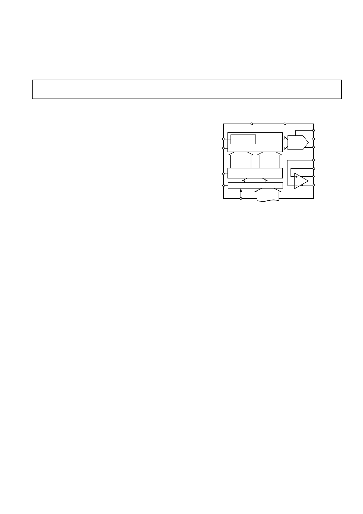
CMOS 180 MHz
DDS/DAC Synthesizer
FUNCTIONAL BLOCK DIAGRAM
32-BIT
TUNING
WORD
PHASE
AND
CONTROL
WORDS
FREQUENCY/PHASE
DATA REGISTER
DATA INPUT REGISTER
10-BIT
DAC
DAC R
SET
ANALOG
OUT
ANALOG
IN
CLOCK OUT
CLOCK OUT
HIGH SPEED
DDS
FREQUENCY
UPDATE/DATA
REGISTER
RESET
WORD LOAD
CLOCK
MASTER
RESET
REF
CLOCK IN
63 REFCLK
MULTIPLIER
COMPARATOR
SERIAL
LOAD
1 BIT 3
40 LOADS
PARALLEL
LOAD
8 BITS 3
5 LOADS
FREQUENCY, PHASE
AND CONTROL DATA INPUT
AD9851
+V
S
GND
FEATURES
180 MHz Clock Rate with Selectable 6ⴛ Reference Clock
Multiplier
On-Chip High Performance 10-Bit DAC and High Speed
Comparator with Hysteresis
SFDR >43 dB @ 70 MHz A
OUT
32-Bit Frequency Tuning Word
Simplified Control Interface: Parallel or Serial
Asynchronous Loading Format
5-Bit Phase Modulation and Offset Capability
Comparator Jitter <80 ps p-p @ 20 MHz
+2.7 V to +5.25 V Single Supply Operation
Low Power: 555 mW @ 180 MHz
Power-Down Function, 4 mW @ +2.7 V
Ultrasmall 28-Lead SSOP Packaging
APPLICATIONS
Frequency/Phase-Agile Sine Wave Synthesis
Clock Recovery and Locking Circuitry for Digital
Communications
Digitally Controlled ADC Encode Generator
Agile L.O. Applications in Communications
Quadrature Oscillator
CW, AM, FM, FSK, MSK Mode Transmitter
GENERAL DESCRIPTION
The AD9851 is a highly integrated device that uses advanced
DDS technology, coupled with an internal high speed, high
performance D/A converter, and comparator, to form a digitallyprogrammable frequency synthesizer and clock generator function. When referenced to an accurate clock source, the AD9851
generates a stable frequency and phase-programmable digitized
analog output sine wave. This sine wave can be used directly as
a frequency source, or internally converted to a square wave for
agile-clock generator applications. The AD9851’s innovative
high speed DDS core accepts a 32-bit frequency tuning word,
which results in an output tuning resolution of approximately
0.04 Hz with a 180 MHz system clock. The AD9851 contains a
unique 6× REFCLK Multiplier circuit that eliminates the need
for a high speed reference oscillator. The 6× REFCLK Multiplier
has minimal impact on SFDR and phase noise characteristics.
The AD9851 provides five bits of programmable phase modulation resolution to enable phase shifting of its output in incre-
ments of 11.25°.
The AD9851 contains an internal high speed comparator that
can be configured to accept the (externally) filtered output of
the DAC to generate a low jitter output pulse.
The frequency tuning, control and phase modulation words are
asynchronously loaded into the AD9851 via parallel or serial
loading format. The parallel load format consists of five iterative loads of an 8-bit control word (byte). The first 8-bit byte
controls output phase, 6× REFCLK Multiplier, power-down
enable and loading format; the remaining bytes comprise the
32-bit frequency tuning word. Serial loading is accomplished
via a 40-bit serial data stream entering through one of the parallel
input bus lines. The AD9851 uses advanced CMOS technology
to provide this breakthrough level of functionality on just 555 mW
of power dissipation (+5 V supply), at the maximum clock rate of
180 MHz.
The AD9851 is available in a space-saving 28-lead SSOP, surface mount package that is pin-for-pin compatible with the
popular AD9850 125 MHz DDS. It is specified to operate over
the extended industrial temperature range of –40°C to +85°C at
>3.0 V supply voltage. Below 3.0 V, the specifications apply
over the commercial temperature range of 0°C to +85°C.

–2– REV. C
AD9851–SPECIFICATIONS
Test AD9851BRS
P
arameter Temp Level Min Typ Max Units
CLOCK INPUT CHARACTERISTICS
Frequency Range (6× REFCLK Multiplier Disabled)
+5.0 V Supply FULL IV 1 180 MHz
+3.3 V Supply FULL IV 1 125 MHz
+2.7 V Supply 0°C to +85°C IV 1 100 MHz
Frequency Range (6× REFCLK Multiplier Enabled)
+5.0 V Supply FULL IV 5 30 MHz
+3.3 V Supply FULL IV 5 20.83 MHz
+2.7 V Supply 0°C to +85°C IV 5 16.66 MHz
Input Resistance +25°CV 1 MΩ
Minimum Switching Thresholds
2
Logic “1,” +5.0 V Supply +25°CIV3.5 V
Logic “1,” +3.3 V Supply +25°CIV2.3 V
Logic “0,” +5.0 V Supply +25°CIV 1.5V
Logic “0,” +3.3 V Supply +25°CIV 1 V
DAC OUTPUT CHARACTERISTICS
Full-Scale Output Current +25°C IV 5 10 20 mA
Gain Error +25°C I –10 10 % FS
Output Offset +25°CI 10µA
Differential Nonlinearity +25°C I 0.75 LSB
Integral Nonlinearity +25°C I 1 LSB
Residual Phase Noise, 5.2 MHz, 1 kHz Offset
PLL On +25°C V –125 dBc/Hz
PLL Off +25°C V –132 dBc/Hz
Output Impedance +25°C V 120 kΩ
Voltage Compliance Range +25°C I –0.5 1.5 V
Wideband Spurious-Free Dynamic Range
1.1 MHz Analog Out (DC to 72 MHz) +25°C IV 60 64 dBc
20.1 MHz Analog Out (DC to 72 MHz) +25°C IV 51 53 dBc
40.1 MHz Analog Out (DC to 72 MHz) +25°C IV 51 55 dBc
50.1 MHz Analog Out (DC to 72 MHz) +25°C IV 46 53 dBc
70.1 MHz Analog Out (DC to 72 MHz) +25°C IV 42 43 dBc
Narrowband Spurious-Free Dynamic Range
1.1 MHz (±50 kHz) +25°C V 85 dBc
1.1 MHz (±200 kHz) +25°C V 80 dBc
40.1 MHz (±50 kHz) +25°C V 85 dBc
40.1 MHz (±200 kHz) +25°C V 80 dBc
70.1 MHz (±50 kHz) +25°C V 85 dBc
70.1 MHz (±200 kHz) +25°C V 73 dBc
COMPARATOR INPUT CHARACTERISTICS
Input Capacitance +25°CV 3 pF
Input Resistance +25°C IV 500 kΩ
Input Bias Current +25°CI 12 µA
Input Voltage Range +25°CIV0 5 V
COMPARATOR OUTPUT CHARACTERISTICS
Logic “1” Voltage +5 V Supply +25°C VI +4.8 V
Logic “1” Voltage +3.3 V Supply +25°C VI +3.1 V
Logic “1” Voltage +2.7 V Supply +25°C VI +2.3 V
Logic “0” Voltage +25°C VI +0.4 V
Continuous Output Current +25°CIV 20mA
Hysteresis +25°CIV10 mV
Propagation Delay +25°CIV 7 ns
Toggle Frequency (1 V p-p Input Sine Wave) +25°C IV 200 MHz
Rise/Fall Time, 15 pF Output Load +25°CIV 7 ns
Output Jitter (p-p)
3
+25°C IV 80 ps (p-p)
CLOCK OUTPUT CHARACTERISTICS
Output Jitter (Clock Generator Configuration,
40 MHz 1 V p-p Input Sine Wave) +25°C V 250 ps (p-p)
Clock Output Duty Cycle FULL IV 50 ± 10 %
(V
S1
= +5 V ⴞ 5%, R
SET
= 3.9 k⍀, 6ⴛ REFCLK Multiplier Disabled, External Reference
Clock = 180 MHz except as noted)

–3–REV. C
AD9851
Test AD9851BRS
Parameter Temp Level Min Typ Max Units
TIMING CHARACTERISTICS
4
tWH, tWL (W_CLK Min Pulsewidth High/Low) FULL IV 3.5 ns
t
DS
, tDH (Data to W_CLK Setup and Hold Times) FULL IV 3.5 ns
t
FH
, tFL (FQ_UD Min Pulsewidth High/Low) FULL IV 7 ns
t
CD
(REFCLK Delay After FQ_UD)
5
FULL IV 3.5 ns
t
FD
(FQ_UD Min Delay After W_CLK) FULL IV 7 ns
t
CF
(Output Latency from FQ_UD)
Frequency Change FULL IV 18 SYSCLK
Cycles
Phase Change FULL IV 13 SYSCLK
Cycles
t
RH
(CLKIN Delay After RESET Rising Edge) FULL IV 3.5 ns
t
RL
(RESET Falling Edge After CLKIN) FULL IV 3.5 ns
t
RR
(Recovery from RESET) FULL IV 2 SYSCLK
Cycles
t
RS
(Minimum RESET Width) FULL IV 5 SYSCLK
Cycles
t
OL
(RESET Output Latency) FULL IV 13 SYSCLK
Cycles
Wake-Up Time from Power-Down Mode
6
+25°CV 5 µs
CMOS LOGIC INPUTS
Logic “1” Voltage, +5 V Supply +25°CI 3.5 V
Logic “1” Voltage, +3.3 V Supply +25°CI 3.0 V
Logic “1” Voltage, +2.7 V Supply +25°CI 2.4 V
Logic “0” Voltage +25°CI 0.4 V
Logic “1” Current +25°CI 12 µA
Logic “0” Current +25°CI 12 µA
Rise/Fall Time +25°C IV 100 ns
Input Capacitance +25°CV 3 pF
POWER SUPPLY
V
S
6
Current @:
62.5 MHz Clock, +2.7 V Supply +25°CVI 3035mA
100 MHz Clock, +2.7 V Supply +25°CVI 4050mA
62.5 MHz Clock, +3.3 V Supply +25°CVI 3545mA
125 MHz Clock, +3.3 V Supply +25°CVI 5570mA
62.5 MHz Clock, +5 V Supply +25°CVI 5065mA
125 MHz Clock, +5 V Supply +25°CVI 7090mA
180 MHz Clock, +5 V Supply +25°C VI 110 130 mA
Power Dissipation @ :
62.5 MHz Clock, +5 V Supply +25°C VI 250 325 mW
62.5 MHz Clock, +3.3 V Supply +25°C VI 115 150 mW
62.5 MHz Clock, +2.7 V Supply +25°CVI 8595mW
100 MHz Clock, +2.7 V Supply +25°C VI 110 135 mW
125 MHz Clock, +5 V Supply +25°C VI 365 450 mW
125 MHz Clock, +3.3 V Supply +25°C VI 180 230 mW
180 MHz Clock, +5 V Supply +25°C VI 555 650 mW
P
DISS
Power-Down Mode @:
+5 V Supply +25°CVI 1755mW
+2.7 V Supply +25°CVI 4 20 mW
NOTES
1
+VS collectively refers to the positive voltages applied to DVDD, PVCC and AVDD. Voltages applied to these pins should be of the same potential.
2
Indicates the minimum signal levels required to reliably clock the device at the indicated supply voltages. This specifies the p-p signal level and dc offset needed when
the clocking signal is not of CMOS/TTL origin, i.e., a sine wave with 0 V dc offset.
3
The comparator’s jitter contribution to any input signal. This is the minimum jitter on the outputs that can be expected from an ideal input. Considerably more
output jitter is seen when nonideal input signals are presented to the comparator inputs. Nonideal characteristics include the presence of extraneous, nonharmonic
signals (spur’s, noise), slower slew rate and low comparator overdrive.
4
Timing of input signals FQ_UD, WCLK, RESET are asynchronous to the Reference Clock; however, the presence of a Reference Clock is required to implement
those functions. In the absence of a Reference Clock, the AD9851 automatically enters power-down mode rendering the IC, including the comparator, inoperable
until a Reference Clock is restored. Very high speed updates of frequency/phase word will require FQ_UD and WCLK to be externally synchronized with the external Reference Clock to assure proper timing.
5
Not applicable when 6× REFCLK Multiplier is engaged.
6
Assumes no capacitive load on DACBP (Pin 17).
Specifications subject to change without notice.
AD9851
–4– REV. C
CAUTION
ESD (electrostatic discharge) sensitive device. Electrostatic charges as high as 4000 V readily
accumulate on the human body and test equipment and can discharge without detection.
Although the AD9851 features proprietary ESD protection circuitry, permanent damage may
occur on devices subjected to high energy electrostatic discharges. Therefore, proper ESD
precautions are recommended to avoid performance degradation or loss of functionality.
Application Note: Users are cautioned not to apply digital input signals prior to power-up of this
device. Doing so may result in a latch-up condition.
WARNING!
ESD SENSITIVE DEVICE
ABSOLUTE MAXIMUM RATINGS*
Maximum Junction Temperature . . . . . . . . . . . . . . . .+150°C
Storage Temperature . . . . . . . . . . . . . . . . . . –65°C to +150°C
V
S
. . . . . . . . . . . . . . . . . . . . . . . . . . . . . . . . . . . . . . . . . . +6 V
Operating Temperature . . . . . . . . . . . . . . . . . –40°C to +85°C
Digital Inputs . . . . . . . . . . . . . . . . . . . –0.7 V to +V
S
+ 0.7 V
Lead Temperature (10 sec) Soldering . . . . . . . . . . . . .+300°C
Digital Output Current . . . . . . . . . . . . . . . . . . . . . . . . 30 mA
SSOP θ
JA
Thermal Impedance . . . . . . . . . . . . . . . . . . 82°C/W
DAC Output Current . . . . . . . . . . . . . . . . . . . . . . . . . .30 mA
*Absolute maximum ratings are limiting values, to be applied individually, and
beyond which the serviceability of the circuit may be impaired. Functional
operability under any of these conditions is not necessarily implied. Exposure of
absolute maximum rating conditions for extended periods of time may affect
device reliability.
EXPLANATION OF TEST LEVELS
Test Level
I – 100% Production Tested.
III – Sample Tested Only.
IV – Parameter is guaranteed by design and characterization
testing.
V – Parameter is a typical value only.
VI – Devices are 100% production tested at +25°C and
guaranteed by design and characterization testing for
industrial operating temperature range.
ORDERING GUIDE
Model Temperature Range Package Description Package Option
AD9851BRS –40°C to +85°C Shrink Small Outline (SSOP) RS-28
AD9851
–5–REV. C
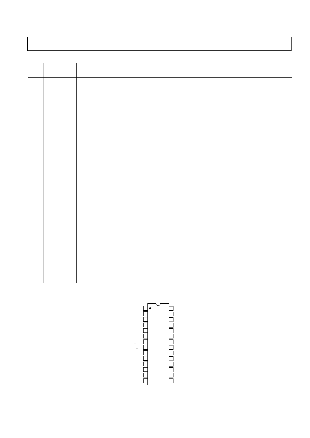
PIN FUNCTION DESCRIPTIONS
Pin
No. Mnemonic Function
4–1, D0–D7 8-Bit Data Input. The data port for loading the 32-bit frequency and 8-bit phase/control words. D7 = MSB;
28–25 D0 = LSB. D7, Pin 25, also serves as the input pin for 40-bit serial data word.
5 PGND 6× REFCLK Multiplier Ground Connection.
6 PVCC 6× REFCLK Multiplier Positive Supply Voltage Pin.
7 W_CLK Word Load Clock. Rising edge loads the parallel or serial frequency/phase/control words asynchronously
into the 40-bit input register.
8 FQ_UD Frequency Update. A rising edge asynchronously transfers the contents of the 40-bit input register to be
acted upon by the DDS core. FQ_UD should be issued when the contents of the input register are known
to contain only valid, allowable data.
9 REFCLOCK Reference Clock Input. CMOS/TTL-level pulse train, direct or via the 6× REFCLK Multiplier. In direct
mode, this is also the SYSTEM CLOCK. If the 6× REFCLK Multiplier is engaged, then the output of the
multiplier is the SYSTEM CLOCK. The rising edge of the SYSTEM CLOCK initiates operations.
10, 19 AGND Analog Ground. The ground return for the analog circuitry (DAC and Comparator).
11, 18 AVDD Positive supply voltage for analog circuitry (DAC and Comparator, Pin 18) and bandgap voltage reference,
Pin 11.
12 R
SET
The DAC’s external R
SET
connection—nominally a 3.92 kΩ resistor to ground for 10 mA out. This sets
the DAC full-scale output current available from IOUT and IOUTB. R
SET
= 39.93/IOUT
13 VOUTN Voltage Output Negative. The comparator’s “complementary” CMOS logic level output.
14 VOUTP Voltage Output Positive. The comparator’s “true” CMOS logic level output.
15 VINN Voltage Input Negative. The comparator’s inverting input.
16 VINP Voltage Input Positive. The comparator’s noninverting input.
17 DACBP DAC Bypass Connection. This is the DAC voltage reference bypass connection normally NC (NO
CONNECT) for optimum SFDR performance.
20 IOUTB The “complementary” DAC output with same characteristics as IOUT except that IOUTB = (full-scale
output–IOUT). Output load should equal that of IOUT for best SFDR performance.
21 IOUT The “true” output of the balanced DAC. Current is “sourcing” and requires current-to-voltage
conversion, usually a resistor or transformer referenced to GND. IOUT = (full-scale output–IOUTB)
22 RESET Master Reset pin; active high; clears DDS accumulator and phase offset register to achieve 0 Hz and 0°
output phase. Sets programming to parallel mode and disengages the 6× REFCLK Multiplier. Reset does
not clear the 40-bit input register. On power-up, asserting RESET should be the first priority before pro-
gramming commences.
23 DVDD Positive supply voltage pin for digital circuitry.
24 DGND Digital Ground. The ground return pin for the digital circuitry.
PIN CONFIGURATION
TOP VIEW
(Not to Scale)
28
27
26
25
24
23
22
21
20
19
18
17
16
15
1
2
3
4
5
6
7
8
9
10
11
12
13
14
AD9851
VOUTP
VOUTN
R
SET
AVDD
AGND
REFCLOCK
FQ UD
D3
D2
D1
LSB D0
PVCC
PGND
VINN
VINP
DACBP
AVDD
AGND
IOUTB
IOUT
D4
D5
D6
D7 MSB/SERIAL LOAD
RESET
DVDD
DGND
W
CLK
AD9851
–6– REV. C
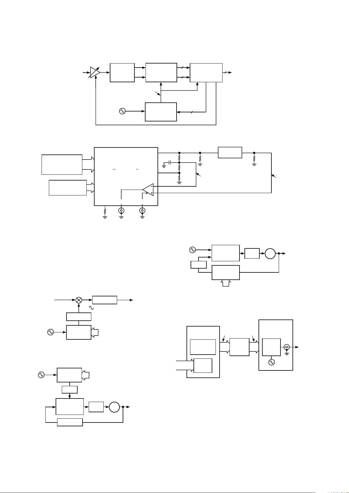
Both IOUT and IOUTB are equally loaded with 100 Ω. Two
100 kΩ resistors “sample” each output and average the two
voltages. The result is filtered with the 470 pF capacitor and
applied to one comparator input as a dc switching threshold.
The filtered DAC sine wave output is applied to the other comparator input. The comparator will toggle with nearly 50% duty
cycle as the sine wave alternately traverses the “center point”
threshold.
AD9851
DDS
REFERENCE
CLOCK
IF FREQUENCY
IN
FILTER
FILTER
TUNING
WORD
RF
FREQUENCY
OUT
Figure 3. Frequency/Phase-Agile Local Oscillator for
Frequency Mixing/Multiplying
FILTER
PHASE
COMPARATOR
DIVIDE-BY-N
LOOP
FILTER
VCO
AD9851
DDS
REFERENCE
CLOCK
TUNING
WORD
RF
FREQUENCY
OUT
Figure 4. Frequency/Phase-Agile Reference for PLL
I/Q MIXER
AND
LOW PASS
FILTER
I
Q
AD9059
DUAL
8-BIT ADC
8
8
DIGITAL
DEMODULATOR
ADC ENCODE
AGC
32
CHIP/SYMBOL/PN
RATE DATA
ADC CLOCK FREQUENCY
LOCKED TO
Tx CHIP/SYMBOL/PN RATE
180MHz
OR 30MHz
REFERENCE
CLOCK
Rx BASEBAND
DIGITAL DATA OUT
Rx
RF IN
VCA
AD9851
CLOCK
GENERATOR
Figure 1. “Chip Rate” Clock Generator Application in a Spread Spectrum Receiver
MICROPROCESSOR
OR
MICROCONTROLLER
DATA
BUS
180MHz OR 30MHz
REFERENCE
CLOCK
8-BIT PARALLEL DATA,
OR 1-BIT 3 40 SERIAL DATA,
RESET, W CLK AND FQ UD
IOUT
100kV
100kV
470pF
100V
IOUTB
R
SET
3.9kV
CMOS
OUTPUTS
QOUTBQOUT
LOW-PASS
FILTER
7TH ORDER ELLIPTICAL
70MHz LOW PASS
200V IMPEDANCE
200V
VOLTAGE HERE = CENTER POINT
OF SINE WAVE (0.5V TYPICALLY)
USING PASSIVE "AVERAGING" CIRCUIT
0 TO 1V p-p
SINE WAVE
AD9851
200V
Figure 2. Basic Clock Generator Configuration
PHASE
COMPARATOR
LOOP
FILTER
VCO
AD9851
DDS
REFERENCE
CLOCK
TUNING
WORD
RF
FREQUENCY
OUT
FILTER
REF CLK IN
PROGRAMMABLE
"DIVIDE-BY-N" FUNCTION
(WHERE N = 2
32
/TUNING WORD)
Figure 5. Digitally-Programmable “Divide-by-N” Function
in PLL
AD9851
DDS
FM RF
OUTPUT
ADSP-2181
DSP
PROCESSOR
ADSP-2181
BUS
INPUT/
OUTPUT
DECODE
LOGIC
8-BIT
DATA
BUS
AD1847
STEREO
CODEC
L & R
AUDIO IN
REF
OSC
DAC
OUT
AD9851/FSPCB
EVALUATION
BOARD
EZ-KIT LITE
DSP
Figure 6. High Quality, All-Digital RF Frequency Modulation
High quality, all digital RF frequency modulation generation
with the ADSP-2181 DSP and the AD9851 DDS. This application is well documented in Analog Devices’ application Note
AN-543, and uses an “image” of the DDS output as illustrated
in Figure 8.
AD9851
–7–REV. C
REF
CLOCK
90
PHASE
DIFFERENCE
8-BIT DATA BUS
FQ UD
RESET
W CLK
AD9851
#2
IOUT
AD9851
#1
W CLK
FQ UD
RESET
IOUT
RESET
FQ
UD
RESET
FQ
UD
W
CLK #2
W CLK #1
MICROPROCESSOR
OR
MICROCONTROLLER
W
CLK #2
W
CLK #1
Figure 7. Application Showing Synchronization of Two
AD9851 DDSs to Form a Quadrature Oscillator
After a common RESET command is issued, separate W_CLKs
allow independent programming of each AD9851 40-bit input
register via the 8-bit data bus or serial input pin. A common
FQ_UD pulse is issued after programming is completed to
simultaneously engage both oscillators at their specified frequency and phase.
AD9851
IOUT
30MHz
CLOCK
BANDPASS
FILTER
50V
50V
FUNDAMENTAL
F
CLK
IMAGE
F
C
– F
O
IMAGE
F
C
+ F
O
AMPLITUDE
60 120 180 240
FREQUENCY – MHz
240
FREQUENCY – MHz
IMAGE
F
C
+ F
O
BANDPASS
FILTER
AMPLITUDE
3 6
AMPLIFIER
240MHz
AD9851
SPECTRUM
FINAL OUTPUT
SPECTRUM
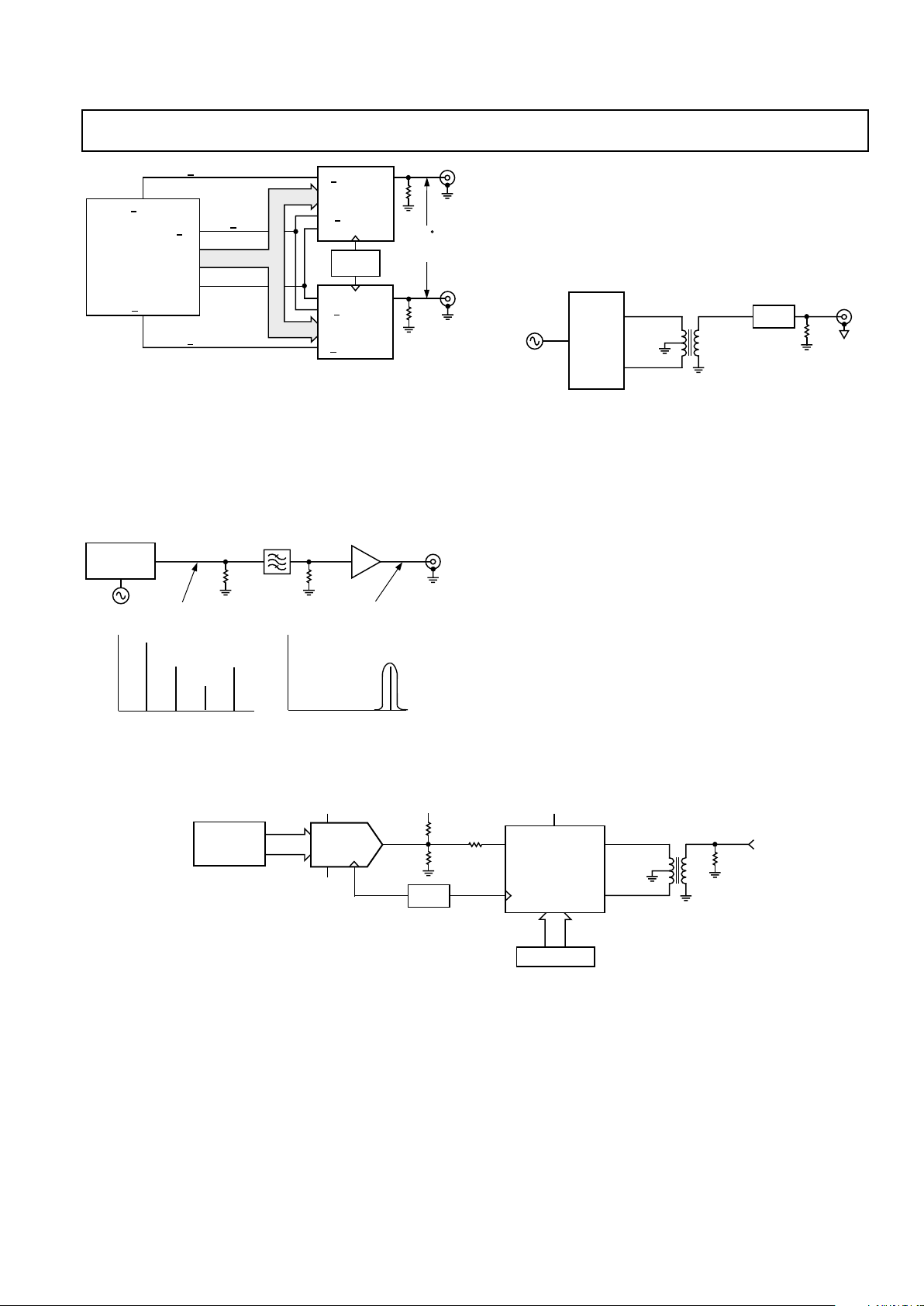
Figure 8. Deriving a High Frequency Output Signal from
the AD9851 by Using an “Alias” or Image Signal
Differential DAC output connection (Figure 9) for reduction of
common-mode signals and to allow highly reactive filters to be
driven without a filter input termination resistor (see above
single-ended example, Figure 8). A 6 dB power advantage is
obtained at the filter output as compared with the single-ended
example, since the filter need not be doubly terminated.
REFERENCE
CLOCK
FILTER
DIFFERENTIAL
TRANSFORMER-COUPLED
OUTPUT
50V
1:1 TRANSFORMER
i.e., MINI-CIRCUITS T1–1T
50V
AD9851
DDS
21
20
Figure 9. Differential DAC Output Connection for Reduction of Common-Mode Signals
The AD9851 R
SET
input being driven by an external DAC
(Figure 10) to provide amplitude modulation or fixed, digital
amplitude control of the DAC output current. Full description
of this application is found as a “Technical Note” on the AD9851
web page (site address is www.analog.com) under “Related
Information.” An Analog Devices application note for the
AD9850, AN-423, describes another method of amplitude
control using an enhancement-mode MOSFET that is equally
applicable to the AD9851.
NOTE: If the 6× REFCLK Multiplier of the AD9851 is en-
gaged, the 125 MHz clocking source shown in Figure 10 can be
reduced by a factor of six.
AD9851
DDS
DIFFERENTIAL
TRANSFORMER-COUPLED
OUTPUT
50V
1:1 TRANSFORMER
50V
IOUT
IOUT
R
SET
+5V
21
20
12
9
4kV
200V
330V
+5V
20mA
MAX
10-BIT DAC
AD9731
+5V
–5V
125MHz
10 BITS
DATA
GENERATOR
e.g., DG-2020
COMPUTER
CONTROL
DATA
Figure 10. The AD9851 R
SET
Input Being Driven by an External DAC
 Loading...