Analog Devices AD9850 h Datasheet
CMOS, 125 MHz
a
FEATURES
125 MHz Clock Rate
On-Chip High Performance DAC and High Speed
Comparator
DAC SFDR > 50 dB @ 40 MHz A
32-Bit Frequency Tuning Word
Simplified Control Interface: Parallel Byte or Serial
Loading Format
Phase Modulation Capability
3.3 V or 5 V Single-Supply Operation
Low Power: 380 mW @ 125 MHz (5 V)
Low Power: 155 mW @ 110 MHz (3.3 V)
Power-Down Function
Ultrasmall 28-Lead SSOP Packaging
APPLICATIONS
Frequency/Phase—Agile Sine Wave Synthesis
Clock Recovery and Locking Circuitry for Digital
Communications
Digitally Controlled ADC Encode Generator
Agile Local Oscillator Applications
OUT
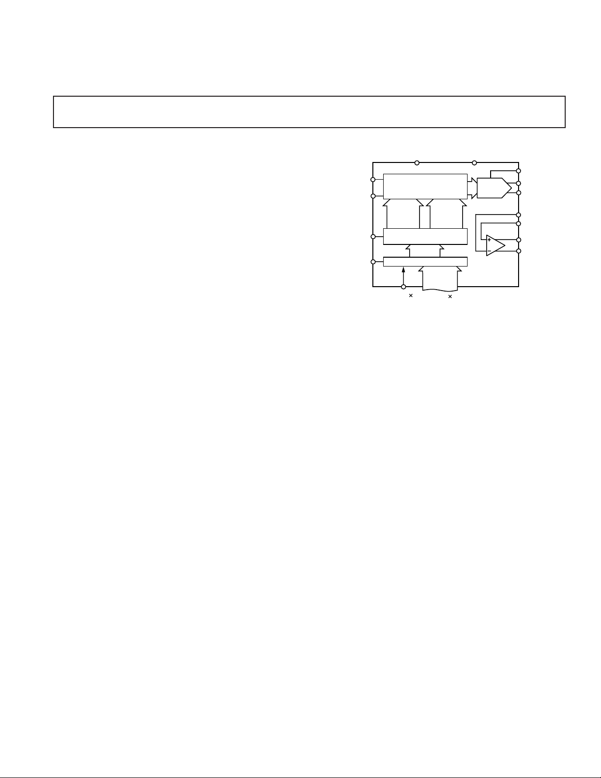
Complete DDS Synthesizer
REF
CLOCK IN
MASTER
RESET
FREQUENCY
UPDATE/
DATA REGISTER
RESET
WORD LOAD
CLOCK
AD9850
FUNCTIONAL BLOCK DIAGRAM
+V
S
HIGH SPEED
DDS
32-BIT
TUNING
WORD
FREQUENCY/PHASE
DATA REGISTER
DATA INPUT REGISTER
SERIAL
LOAD
1-BIT
40 LOADS
FREQUENCY, PHASE, AND CONTROL
DATA INPUT
PHASE
CONTROL
WORDS
PARALLEL
LOAD
8-BITS
5 LOADS
AND
GND
10-BIT
DAC
COMPARATOR
AD9850
DAC R
SET
ANALOG
OUT
ANALOG
IN
CLOCK OUT
CLOCK OUT
GENERAL DESCRIPTION
The AD9850 is a highly integrated device that uses advanced
DDS technology coupled with an internal high speed, high
performance D/A converter and comparator to form a complete, digitally programmable frequency synthesizer and
clock generator function. When referenced to an accurate
clock source, the AD9850 generates a spectrally pure, frequency/phase programmable, analog output sine wave. This
sine wave can be used directly as a frequency source, or it can
be converted to a square wave for agile-clock generator applications. The AD9850’s innovative high speed DDS core provides
a 32-bit frequency tuning word, which results in an output
tuning resolution of 0.0291 Hz for a 125 MHz reference clock
input. The AD9850’s circuit architecture allows the generation
of output frequencies of up to one-half the reference clock
frequency (or 62.5 MHz), and the output frequency can be digitally changed (asynchronously) at a rate of up to 23 million new
frequencies per second. The device also provides five bits of
digitally controlled phase modulation, which enables phase
shifting of its output in increments of 180°, 90°, 45°, 22.5°,
11.25°, and any combination thereof. The AD9850 also contains
a high speed comparator that can be configured to accept the
(externally) filtered output of the DAC to generate a low jitter
square wave output. This facilitates the device’s use as an
agile clock generator function.
The frequency tuning, control, and phase modulation words are
loaded into the AD9850 via a parallel byte or serial loading
format. The parallel load format consists of five iterative loads
of an 8-bit control word (byte). The first byte controls phase
modulation, power-down enable, and loading format; Bytes 2 to
5 comprise the 32-bit frequency tuning word. Serial loading is
accomplished via a 40-bit serial data stream on a single pin. The
AD9850 Complete DDS uses advanced CMOS technology to
provide this breakthrough level of functionality and performance
on just 155 mW of power dissipation (3.3 V supply).
The AD9850 is available in a space-saving 28-lead SSOP,
surface-mount package. It is specified to operate over the
extended industrial temperature range of –40°C to +85°C.
REV. H
Information furnished by Analog Devices is believed to be accurate and
reliable. However, no responsibility is assumed by Analog Devices for its
use, nor for any infringements of patents or other rights of third parties that
may result from its use. No license is granted by implication or otherwise
under any patent or patent rights of Analog Devices. Trademarks and
registered trademarks are the property of their respective owners.
One Technology Way, P.O. Box 9106, Norwood, MA 02062-9106, U.S.A.
Tel: 781/329-4700 www.analog.com
Fax: 781/326-8703 © 2004 Analog Devices, Inc. All rights reserved.

AD9850–SPECIFICATIONS
Parameter Temp Test Level Min Typ Max Unit
CLOCK INPUT CHARACTERISTICS
Frequency Range
5 V Supply Full IV 1 125 MHz
3.3 V Supply Full IV 1 110 MHz
Pulse Width High/Low
5 V Supply 25°CIV 3.2 ns
3.3 V Supply 25°CIV 4.1 ns
DAC OUTPUT CHARACTERISTICS
Full-Scale Output Current
= 3.9 kΩ 25°CV 10.24 mA
R
SET
= 1.95 kΩ 25°CV 20.48 mA
R
SET
Gain Error 25°CI –10 +10 % FS
Gain Temperature Coefficient Full V 150 ppm/°C
Output Offset 25°CI 10 µA
Output Offset Temperature Coefficient Full V 50 nA/°C
Differential Nonlinearity 25°CI 0.5 0.75 LSB
Integral Nonlinearity 25°CI 0.5 1 LSB
Output Slew Rate (50 Ω, 2 pF Load) 25°CV 400 V/µs
Output Impedance 25°CIV 50120 kΩ
Output Capacitance 25°CIV 8 pF
Voltage Compliance 25°CI 1.5 V
Spurious-Free Dynamic Range (SFDR)
Wideband (Nyquist Bandwidth)
1 MHz Analog Out 25°CIV 6372 dBc
20 MHz Analog Out 25°CIV 5058 dBc
40 MHz Analog Out 25°CIV 4654 dBc
Narrowband
40.13579 MHz ± 50 kHz 25°CIV 80 dBc
40.13579 MHz ± 200 kHz 25°CIV 77 dBc
4.513579 MHz ± 50 kHz/20.5 MHz CLK 25°CIV 84 dBc
4.513579 MHz ± 200 kHz/20.5 MHz CLK 25°CIV 84 dBc
COMPARATOR INPUT CHARACTERISTICS
Input Capacitance 25°CV 3 pF
Input Resistance 25°CIV 500 kΩ
Input Current 25°CI –12 +12 µA
Input Voltage Range 25°CIV 0 V
Comparator Offset* Full VI 30 30 mV
COMPARATOR OUTPUT CHARACTERISTICS
Logic 1 Voltage 5 V Supply Full VI 4.8 V
Logic 1 Voltage 3.3 V Supply Full VI 3.1 V
Logic 0 Voltage Full VI 0.4 V
Propagation Delay, 5 V Supply (15 pF Load) 25°CV 5.5 ns
Propagation Delay, 3.3 V Supply (15 pF Load) 25°CV 7 ns
Rise/Fall Time, 5 V Supply (15 pF Load) 25°CV 3 ns
Rise/Fall Time, 3.3 V Supply (15 pF Load) 25°CV 3.5 ns
Output Jitter (p-p) 25°CV 80 ps
CLOCK OUTPUT CHARACTERISTICS
Clock Output Duty Cycle (Clk Gen. Config.) 25°CIV 50 ± 10 %
(VS = 5 V ⴞ 5% except as noted, R
= 3.9 k⍀)
SET
AD9850BRS
DD
V
–2–
REV. H

AD9850
AD9850BRS
Parameter Temp Test Level Min Typ Max Unit
CMOS LOGIC INPUTS (Including CLKIN)
Logic 1 Voltage, 5 V Supply 25°CI 3.5 V
Logic 1 Voltage, 3.3 V Supply 25°CIV 2.4 V
Logic 0 Voltage 25°CIV 0.8 V
Logic 1 Current 25°CI 12µA
Logic 0 Current 25°CI 12µA
Input Capacitance 25°CV 3 pF
POWER SUPPLY (A
Current @
+V
S
62.5 MHz Clock, 3.3 V Supply Full VI 30 48 mA
110 MHz Clock, 3.3 V Supply Full VI 47 60 mA
62.5 MHz Clock, 5 V Supply Full VI 44 64 mA
125 MHz Clock, 5 V Supply Full VI 76 96 mA
@
P
DISS
62.5 MHz Clock, 3.3 V Supply Full VI 100 160 mW
110 MHz Clock, 3.3 V Supply Full VI 155 200 mW
62.5 MHz Clock, 5 V Supply Full VI 220 320 mW
125 MHz Clock, 5 V Supply Full VI 380 480 mW
Power-Down Mode
P
DISS
5 V Supply Full V 30 mW
3.3 V Supply Full V 10 mW
*Tested by measuring output duty cycle variation.
Specifications subject to change without notice.
= 1/3 CLKIN)
OUT
TIMING CHARACTERISTICS*
(VS = 5 V ⴞ 5% except as noted, R
= 3.9 k⍀)
SET
AD9850BRS
Parameter Temp Test Level Min Typ Max Unit
(Data Setup Time) Full IV 3.5 ns
t
DS
t
(Data Hold Time) Full IV 3.5 ns
DH
(W_CLK Minimum Pulse Width High) Full IV 3.5 ns
t
WH
(W_CLK Minimum Pulse Width Low) Full IV 3.5 ns
t
WL
t
(W_CLK Delay after FQ_UD) Full IV 7.0 ns
WD
(CLKIN Delay after FQ_UD) Full IV 3.5 ns
t
CD
(FQ_UD High) Full IV 7.0 ns
t
FH
t
(FQ_UD Low) Full IV 7.0 ns
FL
(Output Latency from FQ_UD)
t
CF
Frequency Change Full IV 18 CLKIN Cycles
Phase Change Full IV 13 CLKIN Cycles
(FQ_UD Minimum Delay after W_CLK) Full IV 7.0 ns
t
FD
(CLKIN Delay after RESET Rising Edge) Full IV 3.5 ns
t
RH
t
(RESET Falling Edge after CLKIN) Full IV 3.5 ns
RL
(Minimum RESET Width) Full IV 5 CLKIN Cycles
t
RS
(RESET Output Latency) Full IV 13 CLKIN Cycles
t
OL
t
(Recovery from RESET) Full IV 2 CLKIN Cycles
RR
Wake-Up Time from Power-Down Mode 25°CV 5 µs
*Control functions are asynchronous with CLKIN.
Specifications subject to change without notice.
REV. H
–3–
AD9850
ABSOLUTE MAXIMUM RATINGS*
Maximum Junction Temperature . . . . . . . . . . . . . . . . 150°C
. . . . . . . . . . . . . . . . . . . . . . . . . . . . . . . . . . . . . . . . . . 6 V
V
DD
Digital Inputs . . . . . . . . . . . . . . . . . . . . . . . . . –0.7 V to +V
Digital Output Continuous Current . . . . . . . . . . . . . . . 5 mA
DAC Output Current . . . . . . . . . . . . . . . . . . . . . . . . . 30 mA
Storage Temperature . . . . . . . . . . . . . . . . . . –65°C to +150°C
Operating Temperature . . . . . . . . . . . . . . . . . –40°C to +85°C
Lead Temperature (Soldering 10 sec) . . . . . . . . . . . . . 300°C
SSOP θ
*Absolute maximum ratings are limiting values, to be applied individually, and
beyond which the serviceability of the circuit may be impaired. Functional
operability under any of these conditions is not necessarily implied. Exposure of
absolute maximum rating conditions for extended periods of time may affect
device reliability.
CAUTION
ESD (electrostatic discharge) sensitive device. Electrostatic charges as high as 4000 V readily
accumulate on the human body and test equipment and can discharge without detection.
Although the AD9850 features proprietary ESD protection circuitry, permanent damage may
occur on devices subjected to high energy electrostatic discharges. Therefore, proper ESD
precautions are recommended to avoid performance degradation or loss of functionality.
Application Note: Users are cautioned not to apply digital input signals prior to power-up of this
device. Doing so may r
Thermal Impedance . . . . . . . . . . . . . . . . . . 82°C/W
JA
esult in a latch-up condition.
ORDERING GUIDE
EXPLANATION OF TEST LEVELS
Test Level
I 100% Production Tested.
III Sample Tested Only.
S
IV Parameter is guaranteed by design and characterization
testing.
V Parameter is a typical value only.
VI All devices are 100% production tested at 25°C. 100%
production tested at temperature extremes for military
temperature devices; guaranteed by design and
characterization testing for industrial devices.
WARNING!
ESD SENSITIVE DEVICE
Model Temperature Range Package Description Package Option
AD9850BRS –40°C to +85°C Shrink Small Outline Package (SSOP) RS-28
AD9850BRS-REEL –40°C to +85°C Shrink Small Outline Package (SSOP) RS-28
AD9850BRSZ* –40°C to +85°C Shrink Small Outline Package (SSOP) RS-28
AD9850BRSZ-REEL* –40°C to +85°C Shrink Small Outline Package (SSOP) RS-28
AD9850/CGPCB Evaluation Board Clock Generator
AD9850/FSPCB Evaluation Board Frequency Synthesizer
*Z = Pb-free part.
–4–
REV. H
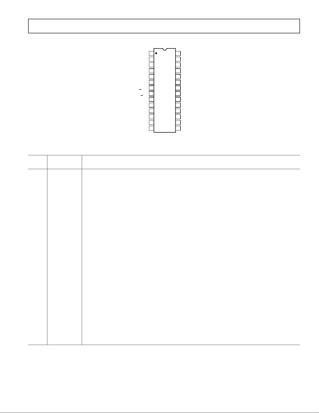
PIN CONFIGURATION
AD9850
1
D3
2
D2
3
D1
4
LSB D0
5
DGND
6
DVDD
CLK
W
FQ
CLKIN
AGND AGND
AVDD
R
QOUTB
QOUT
AD9850
7
TOP VIEW
8
UD
(Not to Scale)
9
10
11
12
SET
13
14
NC = NO CONNECT
D4
28
27
D5
D6
26
25
D7 MSB/SERIAL LOAD
24
DGND
23
DVDD
RESET
22
21
IOUT
20
IOUTB
19
18
AVDD
DACBL (NC)
17
16
VINP
15
VINN
Table I. PIN FUNCTION DESCRIPTIONS
Pin
No. Mnemonic Function
4 to 1, D0 to D7 8-Bit Data Input. This is the 8-bit data port for iteratively loading the 32-bit frequency and the 8-bit phase/
28 to 25 control word. D7 = MSB; D0 = LSB. D7 (Pin 25) also serves as the input pin for the 40-bit serial data-word.
5, 24 DGND Digital Ground. These are the ground return leads for the digital circuitry.
6, 23 DVDD Supply Voltage Leads for Digital Circuitry.
7W_CLK Word Load Clock. This clock is used to load the parallel or serial frequency/phase/control words.
8 FQ_UD Frequency Update. On the rising edge of this clock, the DDS updates to the frequency (or phase)
loaded in the data input register; it then resets the pointer to Word 0.
9 CLKIN Reference Clock Input. This may be a continuous CMOS-level pulse train or sine input biased at
1/2 V supply. The rising edge of this clock initiates operation.
10, 19 AGND Analog Ground. These leads are the ground return for the analog circuitry (DAC and comparator).
11, 18 AVDD Supply Voltage for the Analog Circuitry (DAC and Comparator).
12 R
SET
DAC’s External R
SET
normal applications (F
relationship is I
= 32 (1.248 V/R
OUT
Connection. This resistor value sets the DAC full-scale output current. For
= 10 mA), the value for R
S IOUT
SET
).
is 3.9 kΩ connected to ground. The R
SET
SET/IOUT
13 QOUTB Output Complement. This is the comparator’s complement output.
14 QOUT Output True. This is the comparator’s true output.
15 VINN Inverting Voltage Input. This is the comparator’s negative input.
16 VINP Noninverting Voltage Input. This is the comparator’s positive input.
17 DACBL (NC) DAC Baseline. This is the DAC baseline voltage reference; this lead is internally bypassed and should
normally be considered a no connect for optimum performance.
20 IOUTB Complementary Analog Output of the DAC.
21 IOUT Analog Current Output of the DAC.
22 RESET Reset. This is the master reset function; when set high, it clears all registers (except the input register), and
the DAC output goes to cosine 0 after additional clock cycles—see Figure 7.
REV. H
–5–
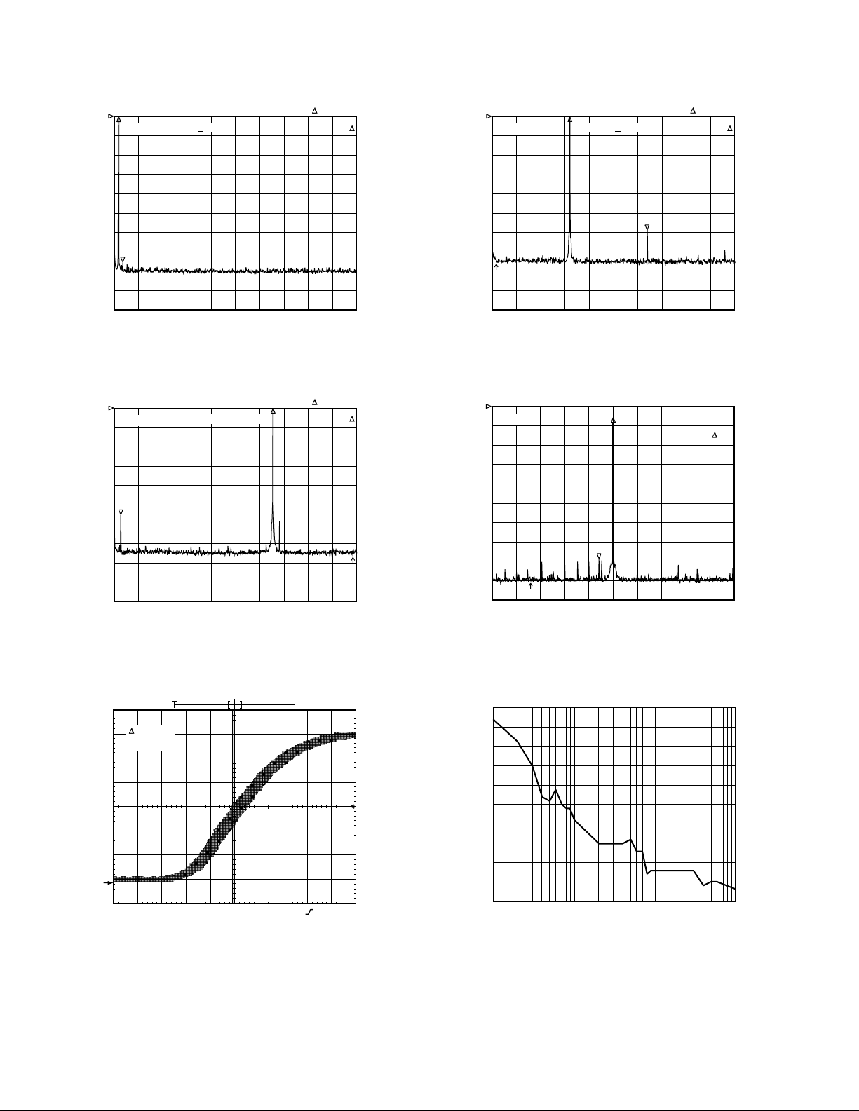
AD9850–Typical Performance Characteristics
CH1 S
RBW # 100Hz
START 0Hz
AD9850
0
Spectrum
CLOCK 125MHz
10dB/REF
VBW 100Hz ATN # 30dB SWP 762 sec
–8.6dBm
TPC 1. SFDR, CLKIN = 125 MHz/f
SSpectrum
CH1
10dB/REF
AD9850
0
–10dBm
CLOCK 125MHz
76.642 dB
Fxd
STOP 62.5MHz
= 1 MHz
OUT
54.818 dB
Fxd
S Spectrum
CH1
RBW # 300Hz
START 0Hz
10dB/REF
AD9850
VBW 300Hz ATN # 30dB SWP 182.6 sec
–10dBm
CLOCK 125MHz
0
TPC 4. SFDR, CLKIN = 125 MHz/f
CH1 S
Spectrum
AD9850
12dB/REF
0dBm –85.401 dB
59.925 dB
STOP 62.5MHz
= 20 MHz
OUT
–23 kHz
Fxd
Mkr
RBW # 300Hz
START 0Hz
TPC 2. SFDR, CLKIN = 125 MHz/f
Tek Run: 100GS/s ET Sample
: 300ps
@: 25.26ns
1
Ch 1 500mV⍀ M 20.0ns Ch 1 1.58V
VBW 300Hz ATN # 30dB SWP 182.6 sec
D 500ps Runs After
STOP 62.5MHz
= 41 MHz
OUT
TPC 3. Typical Comparator Output Jitter,
AD9850 Configured as Clock Generator with
42 MHz LP Filter (40 MHz A
/125 MHz CLKIN)
OUT
0
RBW # 3Hz
CENTER 4.513579MHz
TPC 5. SFDR, CLKIN = 20.5 MHz/f
–105
–110
–115
–120
–125
–130
dBc
–135
–140
–145
–150
–155
100 100k1k
VBW 3Hz ATN # 20dB SWP 399.5 sec
OFFSET FROM 5MHz CARRIER – Hz
SPAN 400kHz
OUT
PN.3RD
10k
= 4.5 MHz
TPC 6. Output Residual Phase Noise (5 MHz
A
/125 MHz CLKIN)
OUT
–6–
REV. H
 Loading...