

REV. 0
Information furnished by Analog Devices is believed to be accurate and
reliable. However, no responsibility is assumed by Analog Devices for its
use, nor for any infringements of patents or other rights of third parties that
may result from its use. No license is granted by implication or otherwise
under any patent or patent rights of Analog Devices.
a
AD9848/AD9849
One Technology Way, P.O. Box 9106, Norwood, MA 02062-9106, U.S.A.
Tel: 781/329-4700 www.analog.com
Fax: 781/326-8703 © Analog Devices, Inc., 2001
CCD Signal Processors with
Integrated Timing Driver
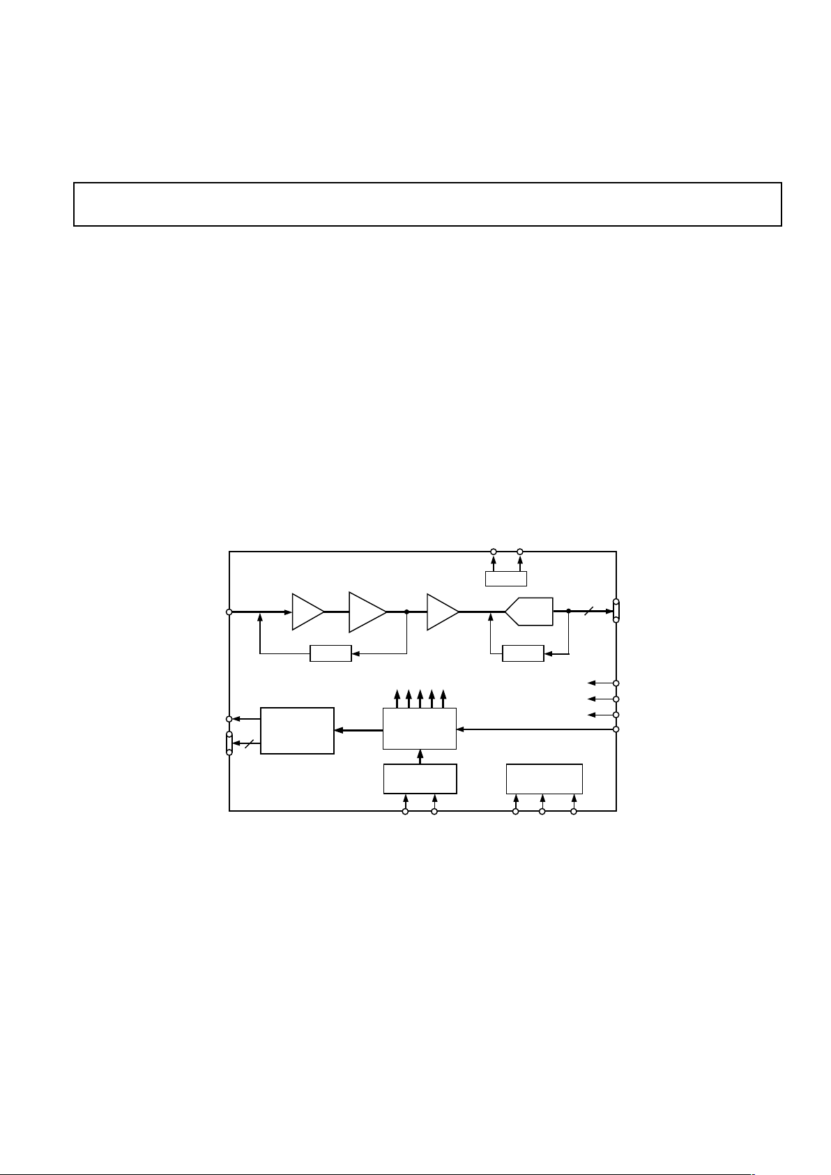
FUNCTIONAL BLOCK DIAGRAM
CLAMP
DOUT
CCDIN
PBLK
VRT
VRB
INTERNAL
REGISTERS
2dB TO 36dB
SYNC
GENERATOR
SDATASCK
SL
CLPOB
10 OR 12
VGA
AD9848/AD9849
4ⴞ6dB
PRECISION
TIMING
TM
CORE
ADC
VREF
CLAMP
INTERNAL
CLOCKS
PxGA
CDS
HORIZONTAL
DRIVERS
4
RG
H1–H4
HD
VD
CLI
CLPDM
FEATURES
AD9848: 10-Bit, 20 MHz Version
AD9849: 12-Bit, 30 MHz Version
Correlated Double Sampler (CDS)
–2 dB to +10 dB Pixel Gain Amplifier (
PxGA
®
)
2 dB to 36 dB 10-Bit Variable Gain Amplifier (VGA)
10-Bit 20 MHz A/D Converter (AD9848)
12-Bit 30 MHz A/D Converter (AD9849)
Black Level Clamp with Variable Level Control
Complete On-Chip Timing Driver
Precision Timing
™
Core with 1 ns Resolution @ 20 MSPS
On-Chip 3 V Horizontal and RG Drivers (AD9848)
On-Chip 5 V Horizontal and RG Drivers (AD9849)
48-Lead LQFP Package
APPLICATIONS
Digital Still Cameras
PRODUCT DESCRIPTION
The AD9848 and AD9849 are highly integrated CCD signal processors for digital still camera applications. Both include a complete
analog front end with A/D conversion, combined with a programmable timing driver. The Precision Timing core allows adjustment
of high speed clocks with approximately 1 ns resolution.
The AD9848 is specified at pixel rates of 20 MHz, and the
AD9849 is specified at 30 MHz. The analog front end includes
black level clamping, CDS, PxGA, VGA, and a 10- or 12-bit A/D
converter. The timing driver provides the high-speed CCD clock
drivers for RG and H1-H4. Operation is programmed using a
3-wire serial interface.
Packaged in a space-saving 48-lead LQFP, the AD9848 and
AD9849 are specified over an operating temperature range of
–20°C to +85°C.
PxGA is a registered trademark and Precision Timing is a trademark of Analog Devices, Inc.

REV. 0
–2–
AD9848/AD9849
–TARGET SPECIFICATIONS
GENERAL SPECIFICATIONS
Parameter Min Typ Max Unit
TEMPERATURE RANGE
Operating –20 +85 °C
Storage –65 +150 °C
MAXIMUM CLOCK RATE
AD9848 20 MHz
AD9849 30 MHz
POWER SUPPLY VOLTAGE, AD9848
Analog (AVDD1, 2, 3) 2.7 3.6 V
Digital1 (DVDD1) H1–H4 2.7 3.6 V
Digital2 (DVDD2) RG 2.7 3.6 V
Digital3 (DVDD3) D0–D11 3.0 V
Digital4 (DVDD4) All Other Digital 3.0 V
POWER SUPPLY VOLTAGE, AD9849
Analog (AVDD1, 2, 3) 2.7 3.6 V
Digital1 (DVDD1) H1–H4 3.0 5.5 V
Digital2 (DVDD2) RG 3.0 5.5 V
Digital3 (DVDD3) D0–D11 3.0 V
Digital4 (DVDD4) All Other Digital 3.0 V
POWER DISSIPATION, AD9848
20 MHz, DVDD1, 2 = 3 V, 100 pF H Loading 220 mW
Total Shutdown Mode 1 mW
POWER DISSIPATION, AD9849
30 MHz, DVDD1, 2 = 5 V, 100 pF H Loading 450 mW
Total Shutdown Mode 1 mW
Specifications subject to change without notice.

REV. 0
–3–
AD9848/AD9849
(T
MIN
to T
MAX
, AVDD1 = DVDD3, DVDD4 = 2.7 V, DVDD1, DVDD2 = 2.7 V [AD9848], DVDD1,
DVDD2 = 5.25 V [AD9849], CL = 20 pF, unless otherwise noted.)
DIGITAL SPECIFICATIONS
Parameter Symbol Min Typ Max Unit
LOGIC INPUTS
High Level Input Voltage V
IH
2.1 V
Low Level Input Voltage V
IL
0.6 V
High Level Input Current I
IH
10 µA
Low Level Input Current I
IL
10 µA
Input Capacitance C
IN
10 pF
LOGIC OUTPUTS
High Level Output Voltage, IOH = 2 mA V
OH
2.2 V
Low Level Output Voltage, IOL = 2 mA V
OL
0.5 V
CLI INPUT
High Level Input Voltage
(AVDD1, 2 +0.5 V) V
IH–CLI
1.85 V
Low Level Input Voltage V
IL–CLI
0.85 V
RG AND H-DRIVER OUTPUTS, AD9848
High Level Output Voltage
(DVDD1, 2 –0.5 V) V
OH
2.2 V
Low Level Output Voltage V
OL
0.5 V
Maximum Output Current (Programmable) 24 mA
Maximum Load Capacitance 100 pF
RG AND H-DRIVER OUTPUTS, AD9849
High Level Output Voltage
(DVDD1, 2 –0.5 V) V
OH
4.75 V
Low Level Output Voltage V
OL
0.5 V
Maximum Output Current (Programmable) 24 mA
Maximum Load Capacitance 100 pF
Specifications subject to change without notice.
REV. 0
–4–
AD9848/AD9849
AD9848–ANALOG SPECIFICATIONS
(T
MIN
to T
MAX
, AVDD = DVDD = 3.0 V, f
CLI
= 20 MHz, unless otherwise noted.)
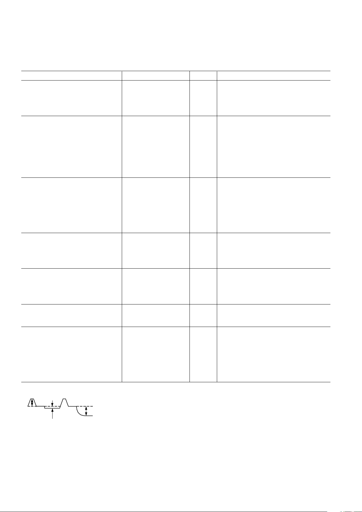
Parameter Min Typ Max Unit Notes
CDS
Gain 0 dB
Allowable CCD Reset Transient
1
500 mV See Input Waveform in Note 1
Max Input Range Before Saturation
1
1.0 V p-p
Max CCD Black Pixel Amplitude
1
150 mV
PIXEL GAIN AMPLIFIER (PxGA)
Max Input Range 1.0 V p-p
Max Output Range 1.6 V p-p
Gain Control Resolution 64 Steps
Gain Monotonicity Guaranteed
Gain Range
Min Gain (32) –2 dB
Med Gain (0) 4 dB Medium Gain (4 dB) Is Default Setting
Max Gain (31) 10 dB
VARIABLE GAIN AMPLIFIER (VGA)
Max Input Range 1.6 V p-p
Max Output Range 2.0 V p-p
Gain Control Resolution 1024 Steps
Gain Monotonicity Guaranteed
Gain Range
Low Gain (91) 2 dB
Max Gain (1023) 36 dB
BLACK LEVEL CLAMP
Clamp Level Resolution 256 Steps
Clamp Level Measured at ADC Output
Min Clamp Level (0) 0 LSB
Max Clamp Level (255) 63.75 LSB
A/D CONVERTER
Resolution 10 Bits
Differential Nonlinearity (DNL) ± 0.4 ± 1.0 LSB
No Missing Codes Guaranteed
Full-Scale Input Voltage 2.0 V
VOLTAGE REFERENCE
Reference Top Voltage (VRT) 2.0 V
Reference Bottom Voltage (VRB) 1.0 V
SYSTEM PERFORMANCE
VGA Gain Accuracy Specifications Include Entire Signal Chain
Gain Includes 4 dB Default PxGA Gain
Low Gain (91) 5 6 7 dB
Max Gain (1023) 38 39.5 41 dB
Peak Nonlinearity, 500 mV Input Signal 0.2 % 12 dB Gain Applied
Total Output Noise 0.2 LSB rms AC Grounded Input, 6 dB Gain Applied
Power Supply Rejection (PSR) 40 dB Measured with Step Change on Supply
NOTES
1
Input signal characteristics defined as follows:
500mV TYP
RESET
TRANSIENT
150mV MAX
OPTICAL
BLACK PIXEL
1V MAX
INPUT
SIGNAL RANGE
Specifications subject to change without notice.
REV. 0
–5–
AD9848/AD9849
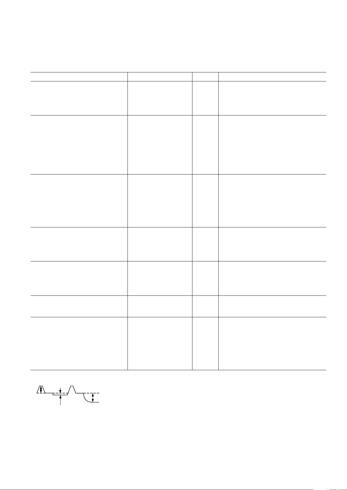
AD9849–ANALOG SPECIFICATIONS
(T
MIN
to T
MAX
, AVDD = DVDD = 3.0 V, f
CLI
= 30 MHz, unless otherwise noted.)
Parameter Min Typ Max Unit Notes
CDS
Gain 0 dB
Allowable CCD Reset Transient
1
500 mV See Input Waveform in Note 1
Max Input Range Before Saturation
1
1.0 V p-p
Max CCD Black Pixel Amplitude
1
150 mV
PIXEL GAIN AMPLIFIER (PxGA)
Max Input Range 1.0 V p-p
Max Output Range 1.6 V p-p
Gain Control Resolution 64 Steps
Gain Monotonicity Guaranteed
Gain Range
Min Gain (32) –2 dB
Med Gain (0) 4 dB Medium Gain (4 dB) Is Default Setting
Max Gain (31) 10 dB
VARIABLE GAIN AMPLIFIER (VGA)
Max Input Range 1.6 V p-p
Max Output Range 2.0 V p-p
Gain Control Resolution 1024 Steps
Gain Monotonicity Guaranteed
Gain Range
Low Gain (91) 2 dB
Max Gain (1023) 36 dB
BLACK LEVEL CLAMP
Clamp Level Resolution 256 Steps
Clamp Level Measured at ADC Output
Min Clamp Level (0) 0 LSB
Max Clamp Level (255) 255 LSB
A/D CONVERTER
Resolution 12 Bits
Differential Nonlinearity (DNL) ± 0.5 ± 1.0 LSB
No Missing Codes Guaranteed
Full-Scale Input Voltage 2.0 V
VOLTAGE REFERENCE
Reference Top Voltage (VRT) 2.0 V
Reference Bottom Voltage (VRB) 1.0 V
SYSTEM PERFORMANCE
Gain Accuracy Specifications Include Entire Signal Chain
Gain Includes 4 dB Default PxGA Gain
Low Gain (91) 5 6 7 dB
Max Gain (1023) 38 39.5 41 dB
Peak Nonlinearity, 500 mV Input Signal 0.2 % 12 dB Gain Applied
Total Output Noise 0.6 LSB rms AC Grounded Input, 6 dB Gain Applied
Power Supply Rejection (PSR) 40 dB Measured with Step Change on Supply
NOTES
1
Input signal characteristics defined as follows:
500mV TYP
RESET
TRANSIENT
150mV MAX
OPTICAL
BLACK PIXEL
1V MAX
INPUT
SIGNAL RANGE
Specifications subject to change without notice.

REV. 0
–6–
AD9848/AD9849
TIMING SPECIFICATIONS
(CL = 20 pF, f
CLI
= 20 MHz [AD9848] or 30 MHz [AD9849], Serial Timing in Figure 3, unless
otherwise noted.)
Parameter Symbol Min Typ Max Unit
MASTER CLOCK (CLI), AD9848
CLI Clock Period t
CLI
50 ns
CLI High/Low Pulsewidth t
ADC
25 ns
Delay From CLI to Internal Pixel Period Position t
CLIDLY
6ns
MASTER CLOCK (CLI), AD9849
CLI Clock Period t
CONV
33.33 ns
CLI High/Low Pulsewidth t
ADC
16.67 ns
EXTERNAL MODE CLAMPING
CLPDM Pulsewidth t
CDM
4 10 Pixels
CLPOB Pulsewidth
1
t
COB
2 20 Pixels
SAMPLE CLOCKS
SHP Rising Edge to SHD Rising Edge (AD9848) t
S1
20 ns
SHP Rising Edge to SHD Rising Edge (AD9849) t
S1
13 ns
DATA OUTPUTS
Output Delay from Programmed Edge t
OD
6ns
Pipeline Delay 9 Cycles
SERIAL INTERFACE
Maximum SCK Frequency f
SCLK
10 MHz
SL to SCK Setup Time t
LS
10 ns
SCK to SL Hold Time t
LH
10 ns
SDATA Valid to SCK Rising Edge Setup t
DS
10 ns
SCK Falling Edge to SDATA Valid Hold t
DH
10 ns
SCK Falling Edge to SDATA Valid Read t
DV
10 ns
NOTES
1
Maximum CLPOB pulsewidth is for functional operation only. Wider typical pulses are recommended to achieve low noise clamp reference.
Specifications subject to change without notice.
REV. 0
AD9848/AD9849
–7–
ORDERING GUIDE
Temperature Package Package
Model Range Description Option
AD9848KST –20°C to +85°C Thin Plastic Quad Flatpack (LQFP) ST-48
AD9849KST –20°C to +85°C Thin Plastic Quad Flatpack (LQFP) ST-48
ABSOLUTE MAXIMUM RATINGS
With
Respect
Parameter To Min Max Unit
AVDD1, 2, 3 AVSS –0.3 +3.9 V
DVDD1, DVDD2 (AD9848) DVSS –0.3 +3.9 V
DVDD1, DVDD2 (AD9849) DVSS –0.3 +5.5 V
DVDD3, 4 DVSS –0.3 +3.9 V
Digital Outputs DVSS3 –0.3 DVDD3 + 0.3 V
CLPOB, CLPDM, BLK DVSS4 –0.3 DVDD4 + 0.3 V
CLI AVSS –0.3 AVDD + 0.3 V
SCK, SL, SDATA DVSS4 –0.3 DVDD4 + 0.3 V
VRT, VRB AVSS –0.3 AVDD + 0.3 V
BYP1 – 3, CCDIN AVSS –0.3 AVDD + 0.3 V
Junction Temperature 150 °C
Lead Temperature (10 sec) 300 °C
CAUTION
ESD (electrostatic discharge) sensitive device. Electrostatic charges as high as 4000 V readily
accumulate on the human body and test equipment and can discharge without detection. Although
the AD9848/AD9849 features proprietary ESD protection circuitry, permanent damage may occur
on devices subjected to high-energy electrostatic discharges. Therefore, proper ESD precautions
are recommended to avoid performance degradation or loss of functionality.
WARNING!
ESD SENSITIVE DEVICE
THERMAL CHARACTERISTICS
Thermal Resistance
48-Lead LQFP Package
JA
= 92°C
REV. 0
AD9848/AD9849
–8–
36
35
34
33
32
31
30
29
28
27
26
25
13 14 15 16 17 18 19 20 21 22 23 24
1
2
3
4
5
6
7
8
9
10
11
12
48 47 46 45 44 39 38 3743 42 41 40
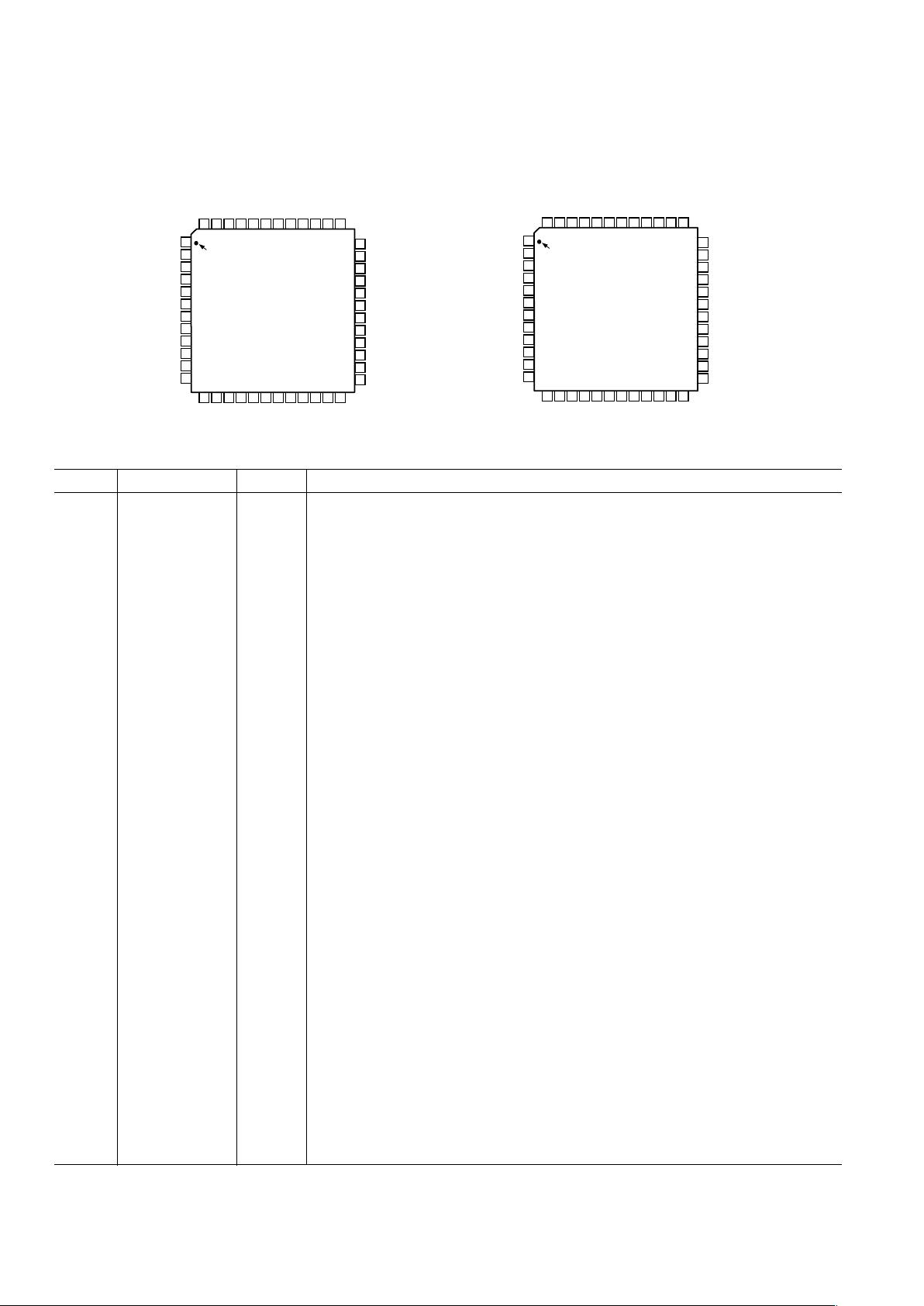
PIN 1
IDENTIFIER
TOP VIEW
(Not to Scale)
SL
REFT
REFB
CMLEVEL
AVSS3
AVDD3
CCDIN
(LSB) D0
D1
D2
D3
D4
NC = NO CONNECT
DVSS3
DVDD3
D5
D6
BYP2
AVDD2
AD9848
D7
AVSS2
NCNCDVDD4
DVSS4HDVD
PBLK
HBLK
CLPDM
CLPOB
SCK
SDI
H1
H2
DVSS1
DVDD1
H3
H4
DVSS2
RG
DVDD2
AVSS1
CLI
AVDD1
D8
(MSB) D9
BYP1
BYP3
36
35
34
33
32
31
30
29
28
27
26
25
13 14 15 16 17 18 19 20 21 22 23 24
1
2
3
4
5
6
7
8
9
10
11
12
48 47 46 45 44 39 38 3743 42 41 40
PIN 1
IDENTIFIER
TOP VIEW
(Not to Scale)
SL
REFT
REFB
CMLEVEL
AVSS3
AVDD3
CCDIN
D2
D3
D4
DVSS3
DVDD3
D5
D6
BYP2
AVDD2
AD9849
D7
AVSS2
D1
D0 (LSB)
DVDD4
DVSS4HDVD
PBLK
HBLK
CLPDM
CLPOB
SCK
SDI
H1
H2
DVSS1
DVDD1
H3
H4
DVSS2
RG
DVDD2
AVSS1
CLI
AVDD1
D8
(MSB) D11
BYP1
BYP3
D9
D10
PIN FUNCTION DESCRIPTIONS
Pin Mnemonic Type Description
1–5 D0–D4 DO Data Outputs AD9848 Only
1–5 D2–D6 DO Data Outputs AD9849 Only
6 DVSS3 P Digital Ground 3 – Data Outputs
7 DVDD3 P Digital Supply 3 – Data Outputs
8–12 D5–D9 DO Data Outputs (D9 is MSB) AD9848 Only
8–12 D7–D11 DO Data Outputs (D9 is MSB) AD9849 Only
13, 14 H1, H2 DO Horizontal Clocks (to CCD)
15 DVSS1 P Digital Ground 1 – H Drivers
16 DVDD1 P Digital Supply 1 – H Drivers
17, 18 H3, H4 DO Horizontal Clocks (to CCD)
19 DVSS2 P Digital Ground 1 – H Drivers
20 RG DO Reset Gate Clock (to CCD)
21 DVDD2 P Digital Supply 2 – RG Driver
22 AVSS1 P Analog Ground 1
23 CLI DI Master Clock Input
24 AVDD1 P Analog Supply 1
25 AVSS2 P Analog Ground 2
26 AVDD2 P Analog Supply 2
27 BYP1 AO Bypass Pin (0.1 µF to AVSS)
28 BYP2 AO Bypass Pin (0.1 µF to AVSS)
29 CCDIN AI Analog Input for CCD Signal
30 BYP3 AO Bypass Pin (0.1 µF to AVSS)
31 AVDD3 P Analog Supply 3
32 AVSS3 P Analog Ground 3
33 CMLEVEL AO Internal Bias Level Decoupling (0.1 µF to AVSS)
34 REFB AO Reference Bottom Decoupling (1.0 µF to AVSS)
35 REFT AO Reference Top Decoupling (1.0 µF to AVSS)
36 SL DI 3-Wire Serial Load (from µP)
37 SDI DI 3-Wire Serial Data Input (from µP)
38 SCK DI 3-Wire Serial Clock (from µP)
39 CLPOB DI Optical Black Clamp Pulse
40 CLPDM DI Dummy Black Clamp Pulse
41 HBLK DI HCLK Blanking Pulse
42 PBLK DI Preblanking Pulse
43 VD DI Vertical Sync Pulse
44 HD DI Horizontal Sync Pulse
45 DVSS4 P Digital Ground 4 – VD, HD, CLPOB, CLPDM, HBLK, PBLK, SCK, SL, SDATA
46 DVDD4 P Digital Supply 4 – VD, HD, CLPOB, CLPDM, HBLK, PBLK, CK, SL, SDATA
47, 48 NC NC Internally Not Connected AD9848 Only
47, 48 D0, D1 DO Data Output (D0 is LSB) AD9849 Only
NOTE
Type: AI = Analog Input, AO = Analog Output, DI = Digital Input, DO = Digital Output, P = Power
PIN CONFIGURATION
REV. 0
–9–
AD9848/AD9849
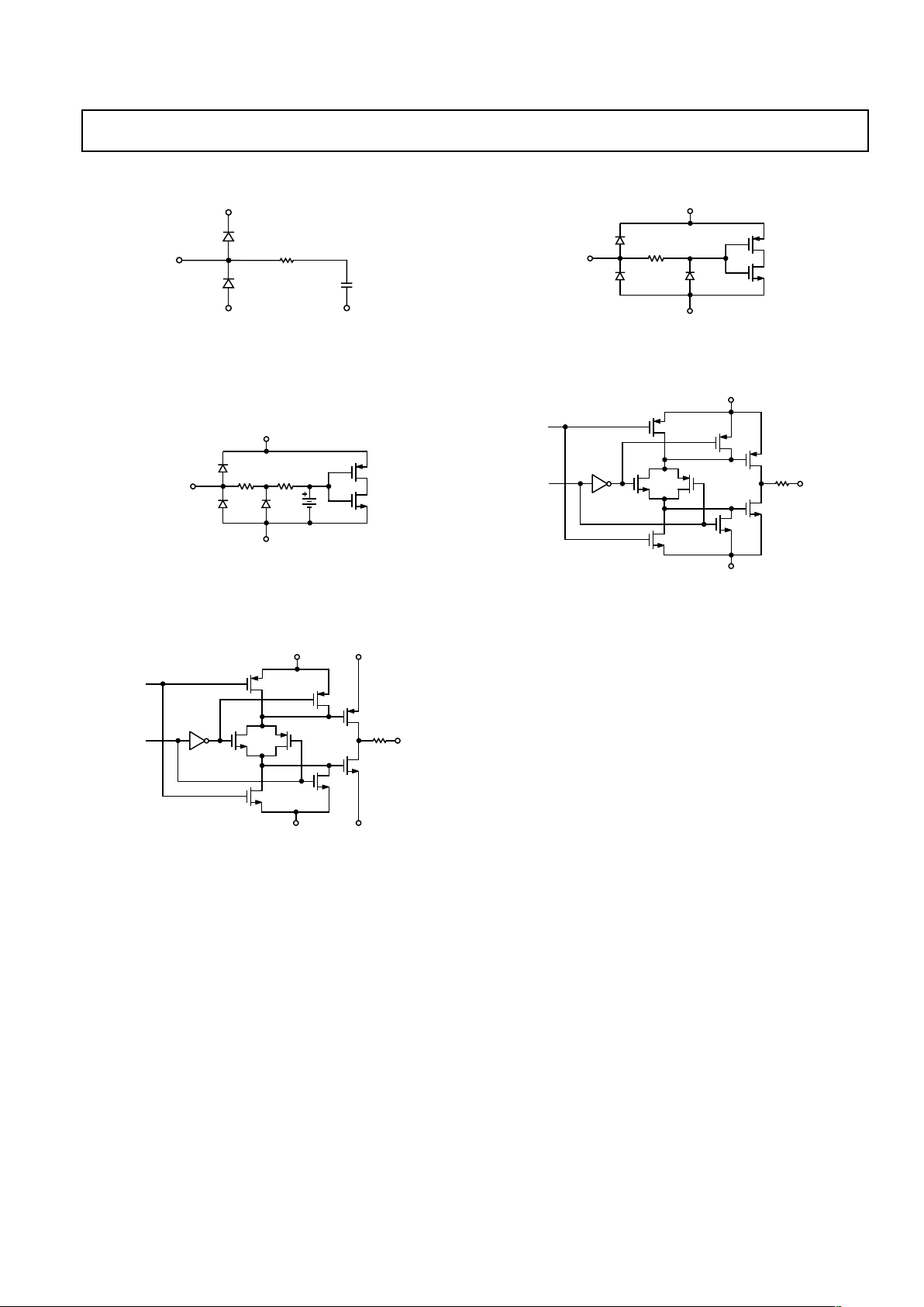
EQUIVALENT INPUT/OUTPUT CIRCUITS
R
AVDD2
AVSS2
AVSS2
Circuit 1. CCDIN (Pin 29)
AVDD1
AVSS1
330⍀
CLI
25k⍀
1.4V
Circuit 2. CLI (Pin 23)
DVDD4 DVDD3
DVSS4 DVSS3
DATA
THREE-
STATE
DOUT
Circuit 3. Data Outputs D0–D11 (Pins 1–5, 8–12, 47–48)
DVDD4
DVSS4
330⍀
Circuit 4. Digital Inputs (Pins 36–44)
DVDD1
DVSS1
DATA
ENABLE
OUTPUT
Circuit 5. H1–H4 and RG (Pins 13, 14, 17, 18, 20)
REV. 0
AD9848/AD9849
–10–
—Typical Linearity and Noise Performance Characteristics
–0.50
0
1000
400
200 600 800
–0.25
0
0.25
0.50
TPC 1. AD9848 Typical DNL
VGA GAIN CODE – LSB
0
0
1000
400
OUTPUT NOISE – LSB
200
1
600 800
2
3
4
TPC 2. AD9848 Output Noise vs. VGA Gain Setting
0
1000
500
1500 2000 2500 3000 3500 4000
0
–0.5
0.5
–0.25
0.25
TPC 3. AD9849 Typical DNL
VGA GAIN CODE – LSB
15
0
0
1000
400
OUTPUT NOISE – LSB
200
5
600
10
800
TPC 4. AD9849 Output Noise vs. VGA Gain Setting
REV. 0
AD9848/AD9849
–11–
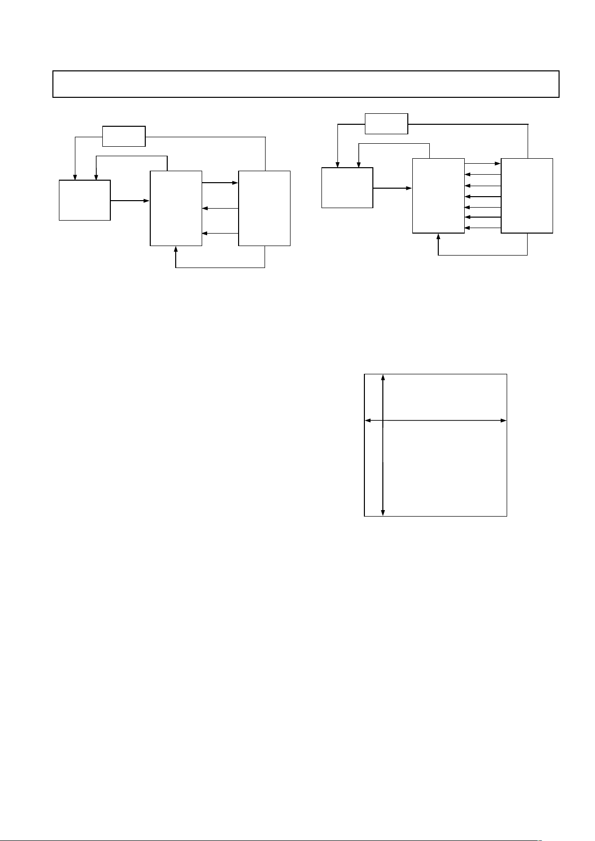
SYSTEM OVERVIEW
CCD
SERIAL
INTERFACE
DOUT
DIGITAL IMAGE
PROCESSING
ASIC
V-DRIVER
HD, VD
CLI
V1–V4, VSG1–VSG8, SUBCK
H1–H4, RG
CCDIN
AD9848/AD9849
INTEGRATED
AFE+TD
Figure 1a. Typical Application (Internal Mode)
CCD
SERIAL
INTERFACE
DOUT
DIGITAL IMAGE
PROCESSING
ASIC
V-DRIVER
HD, VD
CLI
V1–V4, VSG1–VSG8, SUBCK
H1–H4, RG
CCDIN
AD9848/AD9849
INTEGRATED
AFE+TD
PBLK
HBLK
CLPDM
CLPOB
Figure 1b. Typical Application (External Mode)
Figure 1a and 1b show the typical system application diagrams
for the AD9848/AD9849. The CCD output is processed by the
AD9848/AD9849’s AFE circuitry, which consists of a CDS,
PxGA, VGA, black level clamp, and A/D converter. The digitized pixel information is sent to the digital image processor
chip, where all post-processing and compression occurs. To
operate the CCD, CCD timing parameters are programmed
into the AD9848/AD9849 from the image processor, through
the 3-wire serial interface. From the system master clock, CLI,
provided by the image processor, the AD9848/AD9849 generates the high speed CCD clocks and all internal AFE clocks. All
AD9848/AD9849 clocks are synchronized with VD and HD.
Figure 1a shows the AD9848/AD9849 used in Internal mode,
in which all the horizontal pulses (CLPOB, CLPDM, PBLK,
and HBLK) are programmed and generated internally. Figure 1b
shows the AD9848/AD9849 operating in external mode, in
which the horizontal pulses are supplied externally by the
image processor.
The H-drivers for H1–H4 and RG are included in the AD9848/
AD9849, allowing these clocks to be directly connected to the
CCD. H-drive voltage of 5 V is supported in the AD9849.
Figure 2 shows the horizontal and vertical counter dimensions
for the AD9848/AD9849. All internal horizontal clocking is
programmed using these dimensions, to specify line and
pixel locations.
MAXIMUM FIELD DIMENSIONS
12-BIT HORIZONTAL = 4096 PIXELS MAX
12-BIT VERTICAL = 4096 LINES MAX
Figure 2. Vertical and Horizontal Counters

REV. 0
AD9848/AD9849
–12–
SERIAL INTERFACE TIMING
SDATA
A0 A1 A2 A4 A5 A6 A7
D0
D1 D2 D3 D4 D5 XX XX
SCK
SL
A3
NOTES
1. SDATA BITS ARE LATCHED ON SCK RISING EDGES.
2. 14 SCK EDGES ARE NEEDED TO WRITE ADDRESS AND DATA BITS.
3. FOR 16-BIT SYSTEMS, TWO EXTRA DUMMY BITS MAY BE WRITTEN. DUMMY BITS ARE IGNORED.
4. NEW DATA IS UPDATED AT EITHER THE SL RISING EDGE, OR AT THE HD FALLING EDGE AFTER THE NEXT VD FALLING EDGE.
5. VD/HD UPDATE POSITION MAY BE DELAYED TO ANY HD FALLING EDGE IN THE FIELD USING THE UPDATE REGISTER.
VD
HD
SL UPDATED
VD/HD UPDATED
t
DS
t
DH
t
LS
t
LH
Figure 3a. Serial Write Operation
SDATA
A0 A1 A2 A4 A5 A6 A7 D0 D1 D2 D3 D4 D5
SCK
SL
A3
NOTES
1. MULTIPLE SEQUENTIAL REGISTERS MAY BE LOADED CONTINUOUSLY.
2. THE FIRST (LOWEST ADDRESS) REGISTER ADDRESS IS WRITTEN, FOLLOWED BY MULTIPLE 6-BIT DATA WORDS.
3. THE ADDRESS WILL AUTOMATICALLY INCREMENT WITH EACH 6-BIT DATA WORD (ALL 6 BITS MUST BE WRITTEN).
4. SL IS HELD LOW UNTIL THE LAST DESIRED REGISTER HAS BEEN LOADED.
5. NEW DATA IS UPDATED AT EITHER THE SL RISING EDGE, OR AT THE HD FALLING EDGE AFTER THE NEXT VD FALLING EDGE.
D0 D1 D2 D3 D4 D5
D0
...
...
...
DATA FOR STARTING
REGISTER ADDRESS
DATA FOR NEXT
REGISTER ADDRESS
D2D1
Figure 3b. Continuous Serial Write Operation
COMPLETE REGISTER LISTING
Table I
Register Description Register Description
oprmode AFE Operation Modes h1drv H1 Drive Current
ctlmode AFE Control Modes h2drv H2 Drive Current
preventpdate Prevents Loading of VD-Updated Registers h3drv H3 Drive Current
readback Enables Serial Register Readback Mode h4drv H4 Drive Current
vdhdpol VD/HD Active Polarity rgpol RG Polarity
fieldval Internal Field Pulse Value rgposloc RG Positive Edge Location
hblkretime Retimes the H1 hblk to Internal Clock rgnegloc RG Negative Edge Location
tgcore_rstb Reset Bar Signal for Internal TG Core rgdrv RG Drive Current
h12pol H1/H2 Polarity Control shpposloc SHP Sample Location
h1posloc H1 Positive Edge Location shdposloc SHD Sample Location
h1negloc H1 Negative Edge Location
Notes on Register Listing:
1. All addresses and default values are expressed in Hexadecimal.
2. All registers are VD/HD updated as shown in Figure 3, except for the above-listed registers that are SL updated.

REV. 0
AD9848/AD9849
–13–
Bit Default
Address Content Width Value Register Name Register Description
AFE Registers # Bits 56
00 [5:0] 6 00 oprmode[5:0] AFE Operation Mode (See AFE Register Breakdown)
01 [1:0] 2 00 oprmode[7:6]
02 [5:0] 6 16 ccdgain[5:0] VGA Gain
03 [3:0] 4 02 ccdgain[9:6]
04 [5:0] 6 00 refblack[5:0] Black Clamp Level
05 [1:0] 2 02 refblack[7:6]
06 [5:0] 6 00 ctlmode Control Mode (See AFE Register Breakdown)
07 [5:0] 6 00 pxga gain0 PxGA Color 0 Gain
08 [5:0] 6 00 pxga gain1 PxGA Color 1 Gain
09 [5:0] 6 00 pxga gain2 PxGA Color 2 Gain
0A [5:0] 6 00 pxga gain3 PxGA Color 3 Gain
Miscellaneous/Extra # Bits 26
16 [0] 1 00 out_cont Output Control (0 = Make All Outputs DC Inactive)
17 [5:0] 6 00 update[5:0] Serial Data Update Control (Sets the line within the field
18 [5:0] 6 00 update[11:6] for serial data update to occur.)
19 [0] 1 00 preventupdate Prevent the Update of the “VD/HD Updated” Registers
1A [0] 1 00 readback Serial Interface Readback Enable
1B [5:0] 6 00 doutphase DOUT Phase Control
1C [0] 1 00 disablerestore Disable CCDIN DC Restore Circuit During PBLK
(1 = Disable)
1D [0] 1 00 vdhdpol VD/HD Active Polarity (0 = Low Active, 1 = High Active)
1E [0] 1 01 fieldval Internal Field Pulse Value (0 = Next Field Odd,
1 = Next Field Even)
1F [0] 1 00 hblkretime Re-Sync hblk to h1 Clock
20 internal test mode Addresses 20 to 25 Reserved for Internal Test Modes
26 [0] 1 00 tgcore_rstb TG Core Reset_Bar (0 = Hold TG Core in Reset,
1 = Resume Normal Operation)
Notes about Accessing a Double-Wide Register
There are many double-wide registers in the AD9848/AD9849, for example: oprmode, clpdmtog1_0, clpdmscp3, etc. These registers are configured into two consecutive 6-bit registers with the least significant six bits located in the lower of the two addresses and
the remaining most significant bits located in the higher of the two addresses. For example, the 6 LSBs of the clpdmscp3 register, clpdmscp3[5:0], are located at address 0x81. The most significant six bits of the clpdmscp3 register, clpdmscp3[11:6], are
located at address 0x82. The following rules must be followed when accessing double-wide registers:
1. When accessing a double-wide register, BOTH addresses must be written to.
2. The lower of the two consecutive addresses for the double-wide register must be written to first. In the example of the clpdmscp3
register, the contents of address 0x81 must be written first followed by the contents of address 0x82. The register will be updated
after the completion of the write to register 0x82, either at the next SL rising edge or next VD/HD falling edge.
3. A single write to the lower of the two consecutive addresses of a double-wide register that is not followed by a write to the higher
address of the registers, is not permitted. This will not update the register.
4. A single write to the higher of the two consecutive addresses of a double-wide register that is not preceded by a write to the lower
of the two address, is not permitted. Although the write to the higher address will update the full double-wide register, the lower
six bits of the register will be written with an indeterminate value if the lower address was not written first.

REV. 0
AD9848/AD9849
–14–
Bit Default
Address Content Width Value Register Name Register Description
CLPDM # Bits 146
64 [0] 1 01 clpdmdir CLPDM Internal/External (0 = Internal, 1 = External)
65 [0] 1 00 clpdmpol CLPDM External Active Polarity (0 = Low Active,
1 = High Active)
66 [0] 1 01 clpdmspol0 Sequence #0: Start Polarity for CLPDM
67 [5:0] 6 2C clpdmtog1_0[5:0] Sequence #0: Toggle Position 1 for CLPDM
68 [5:0] 6 00 clpdmtog1_0[11:6]
69 [5:0] 6 35 clpdmtog2_0[5:0] Sequence #0: Toggle Position 2 for CLPDM
6A [5:0] 6 00 clpdmtog2_0[11:6]
6B [0] 1 01 clpdmspol1 Sequence #1: Start Polarity for CLPDM
6C [5:0] 6 3E clpdmtog1_1[5:0] Sequence #1: Toggle Position 1 for CLPDM
6D [5:0] 6 02 clpdmtog1_1[11:6]
6E [5:0] 6 16 clpdmtog2_1[5:0] Sequence #1: Toggle Position 2 for CLPDM
6F [5:0] 6 03 clpdmtog2_1[11:6]
70 [0] 1 00 clpdmspol2 Sequence #2: Start Polarity for CLPDM
71 [5:0] 6 3F clpdmtog1_2[5:0] Sequence #2: Toggle Position 1 for CLPDM
72 [5:0] 6 3F clpdmtog1_2[11:6]
73 [5:0] 6 3F clpdmtog2_2[5:0] Sequence #2: Toggle Position 2 for CLPDM
74 [5:0] 6 3F clpdmtog2_2[11:6]
75 [0] 1 01 clpdmspol3 Sequence #3: Start Polarity for CLPDM
76 [5:0] 6 3F clpdmtog1_3[5:0] Sequence #3: Toggle Position 1 for CLPDM
77 [5:0] 6 3F clpdmtog1_3[11:6]
78 [5:0] 6 3F clpdmtog2_3[5:0] Sequence #3: Toggle Position 2 for CLPDM
79 [5:0] 6 3F clpdmtog2_3[11:6]
0 00 clpdmscp0 CLPDM Sequence-Change-Position #0 (Hardcoded to 0)
7A [1:0] 2 00 clpdmsptr0 CLPDM Sequence Pointer for SCP #0
7B [5:0] 6 3F clpdmscp1[5:0] CLPDM Sequence-Change-Position #1
7C [5:0] 6 3F clpdmscp1[11:6]
7D [1:0] 2 00 clpdmsptr1 CLPDM Sequence Pointer for SCP #1
7E [5:0] 6 3F clpdmscp2[5:0] CLPDM Sequence-Change-Position #2
7F [5:0] 6 3F clpdmscp2[11:6]
80 [1:0] 2 00 clpdmsptr2 CLPDM Sequence Pointer for SCP #2
81 [5:0] 6 3F clpdmscp3[5:0] CLPDM Sequence-Change-Position #3
82 [5:0] 6 3F clpdmscp3[11:6]
83 [1:0] 2 00 clpdmsptr3 CLPDM Sequence Pointer for SCP #3

REV. 0
AD9848/AD9849
–15–
Bit Default
Address Content Width Value Register Name Register Description
CLPOB # Bits 146
84 [0] 1 01 clpobdir CLPOB Internal/External (0 = Internal, 1 = External)
85 [0] 1 00 clpobpol CLPOB External Active Polarity (0 = Low Active,
1 = High Active)
86 [0] 1 01 clpobpol0 Sequence #0: Start Polarity for CLPOB
87 [5:0] 6 0E clpobtog1_0[5:0] Sequence #0: Toggle Position 1 for CLPOB
88 [5:0] 6 00 clpobtog1_0[11:6]
89 [5:0] 6 2B clpobtog2_0[5:0] Sequence #0: Toggle Position 2 for CLPOB
8A [5:0] 6 00 clpobtog2_0[11:6]
8B [0] 1 01 clpobpol1 Sequence #1: Start Polarity for CLPOB
8C [5:0] 6 2B clpobtog1_1[5:0] Sequence #1: Toggle Position 1 for CLPOB
8D [5:0] 6 06 clpobtog1_1[11:6]
8E [5:0] 6 3F clpobtog2_1[5:0] Sequence #1: Toggle Position 2 for CLPOB
8F [5:0] 6 3F clpobtog2_1[11:6]
90 [0] 1 00 clpobspol2 Sequence #2: Start Polarity for CLPOB
91 [5:0] 6 3F clpobtog1_2[5:0] Sequence #2: Toggle Position 1 for CLPOB
92 [5:0] 6 3F clpobtog1_2[11:6]
93 [5:0] 6 3F clpobtog2_2[5:0] Sequence #2: Toggle Position 2 for CLPOB
94 [5:0] 6 3F clpobtog2_2[11:6]
95 [0] 1 01 clpobspol3 Sequence #3: Start Polarity for CLPOB
96 [5:0] 6 3F clpobtog1_3[5:0] Sequence #3: Toggle Position 1 for CLPOB
97 [5:0] 6 3F clpobtog1_3[11:6]
98 [5:0] 6 3F clpobtog2_3[5:0] Sequence #3: Toggle Position 2 for CLPOB
99 [5:0] 6 3F clpobtog2_3[11:6]
0 00 clpobscp0 CLPOB Sequence-Change-Position #0 (Hardcoded to 0)
9A [1:0] 2 03 clpobsptr0 CLPOB Sequence Pointer for SCP #0
9B [5:0] 6 01 clpobscp1[5:0] CLPOB Sequence-Change-Position #1
9C [5:0] 6 00 clpobscp1[11:6]
9D [1:0] 2 01 clpobsptr1 CLPOB Sequence Pointer for SCP #1
9E [5:0] 6 02 clpobscp2[5:0] CLPOB Sequence-Change-Position #2
9F [5:0] 6 00 clpobscp2[11:6]
A0 [1:0] 2 00 clpobsptr2 CLPOB Sequence Pointer for SCP #2
A1 [5:0] 6 37 clpobscp3[5:0] CLPOB Sequence-Change-Position #3
A2 [5:0] 6 03 clpobscp3[11:6]
A3 [1:0] 2 03 clpobsptr3 CLPOB Sequence Pointer for SCP #3

REV. 0
AD9848/AD9849
–16–
Bit Default
Address Content Width Value Register Name Register Description
HBLK # Bits 147
A4 [0] 1 01 hblkdir HBLK Internal/External (0 = Internal, 1 = External)
A5 [0] 1 00 hblkpol HBLK External Active Polarity (0 = Low Active,
1 = High Active)
A6 [0] 1 01 hblkextmask HBLK External Masking Polarity (0 = Mask H1 and H3 Low,
1 = Mask H1 and H3 High)
A7 [0] 1 01 hblkmask0 Sequence #0: Masking Polarity for HBLK
A8 [5:0] 6 3E hblktog1_0[5:0] Sequence #0: Toggle High Position for HBLK
A9 [5:0] 6 00 hblktog1_0[11:6]
AA [5:0] 6 0D hblkbtog2_0[5:0] Sequence #0: Toggle Low Position for HBLK
AB [5:0] 6 06 hblkbtog2_0[11:6]
AC [0] 1 01 hblkmask1 Sequence #1: Masking Polarity for HBLK
AD [5:0] 6 38 hblktog1_1[5:0] Sequence #1: Toggle High Position for HBLK
AE [5:0] 6 00 hblktog1_1[11:6]
AF [5:0] 6 3C hblktog2_1[5:0] Sequence #1: Toggle Low Position for HBLK
B0 [5:0] 6 02 hblktog2_1[11:6]
B1 [0] 1 00 hblkmask2 Sequence #2: Masking Polarity for HBLK
B2 [5:0] 6 3F hblktog1_2[5:0] Sequence #2: Toggle High Position for HBLK
B3 [5:0] 6 3F hblktog1_2[11:6]
B4 [5:0] 6 3F hblktog2_2[5:0] Sequence #2: Toggle Low Position for HBLK
B5 [5:0] 6 3F hblktog2_2[11:6]
B6 [0] 1 01 hblkmask3 Sequence #3: Masking Polarity for HBLK
B7 [5:0] 6 3F hblktog1_3[5:0] Sequence #3: Toggle High Position for HBLK
B8 [5:0] 6 3F hblktog1_3[11:6]
B9 [5:0] 6 3F hblktog2_3[5:0] Sequence #3: Toggle Low Position for HBLK
BA [5:0] 6 3F hblktog2_3[11:6]
0 00 hblkscp0 HBLK Sequence-Change-Position #0 (Hardcoded to 0)
BB [1:0] 2 00 hblksptr0 HBLK Sequence Pointer for SCP #0
BC [5:0] 6 3F hblkscp1[5:0] HBLK Sequence-Change-Position #1
BD [5:0] 6 3F hblkscp1[11:6]
BE [1:0] 2 00 hblksptr1 HBLK Sequence Pointer for SCP #1
BF [5:0] 6 3F hblkscp2[5:0] HBLK Sequence-Change-Position #2
C0 [5:0] 6 3F hblkscp2[11:6]
C1 [1:0] 2 00 hblksptr2 HBLK Sequence Pointer for SCP #2
C2 [5:0] 6 3F hblkscp3[5:0] HBLK Sequence-Change-Position #3
C3 [5:0] 6 3F hblkscp3[11:6]
C4 [1:0] 2 00 hblksptr3 HBLK Sequence Pointer for SCP #3

REV. 0
AD9848/AD9849
–17–
Bit Default
Address Content Width Value Register Name Register Description
PBLK # Bits 146
C5 [0] 1 01 pblkdir PBLK Internal/External (0 = Internal, 1 = External)
C6 [0] 1 00 pblkpol PBLK External Active Polarity (0 = Low Active,
1 = High Active)
C7 [0] 1 01 pblkspol0 Sequence #0: Start Polarity for PBLK
C8 [5:0] 6 3D pblktog1_0[5:0] Sequence #0: Toggle Position 1 for PBLK
C9 [5:0] 6 00 pblktog1_0[11:6]
CA [5:0] 6 2A pblkbtog2_0[5:0] Sequence #0: Toggle Position 2 for PBLK
CB [5:0] 6 06 pblkbtog2_0[11:6]
CC [0] 1 00 pblkspol1 Sequence #1: Start Polarity for PBLK
CD [5:0] 6 2A pblktog1_1[5:0] Sequence #1: Toggle Position 1 for PBLK
CE [5:0] 6 06 pblktog1_1[11:6]
CF [5:0] 6 3F pblktog2_1[5:0] Sequence #1: Toggle Position 2 for PBLK
D0 [5:0] 6 3F pblktog2_1[11:6]
D1 [0] 1 00 pblkspol2 Sequence #2: Start Polarity for PBLK
D2 [5:0] 6 3F pblktog1_2[5:0] Sequence #2: Toggle Position 1 for PBLK
D3 [5:0] 6 3F pblktog1_2[11:6]
D4 [5:0] 6 3F pblktog2_2[5:0] Sequence #2: Toggle Position 2 for PBLK
D5 [5:0] 6 3F pblktog2_2[11:6]
D6 [0] 1 01 pblkspol3 Sequence #3: Start Polarity for PBLK
D7 [5:0] 6 3F pblktog1_3[5:0] Sequence #3: Toggle Position 1 for PBLK
D8 [5:0] 6 3F pblktog1_3[11:6]
D9 [5:0] 6 3F pblktog2_3[5:0] Sequence #3: Toggle Position 2 for PBLK
DA [5:0] 6 3F pblktog2_3[11:6]
0 00 pblkscp0 PBLK Sequence-Change-Position #0 (hardcoded to 0)
DB [1:0] 2 02 pblksptr0 PBLK Sequence Pointer for SCP #0
DC [5:0] 6 01 pblkscp1[5:0] PBLK Sequence-Change-Position #1
DD [5:0] 6 00 pblkscp1[11:6]
DE [1:0] 2 01 pblksptr1 PBLK Sequence Pointer for SCP #1
DF [5:0] 6 02 pblkscp2[5:0] PBLK Sequence-Change-Position #2
E0 [5:0] 6 00 pblkscp2[11:6]
E1 [1:0] 2 00 pblksptr2 PBLK Sequence Pointer for SCP #2
E2 [5:0] 6 37 pblkscp3[5:0] PBLK Sequence-Change-Position #3
E3 [5:0] 6 03 pblkscp3[11:6]
E4 [1:0] 2 02 pblksptr3 PBLK Sequence Pointer for SCP #3
H1–H4, RG, SHP, SHD # Bits 53
E5 [0] 1 00 h1pol H1/H2 Polarity Control (0 = No Inversion, 1 = Inversion)
E6 [5:0] 6 00 h1posloc H1 Positive Edge Location
E7 [5:0] 6 20 h1negloc H1 Negative Edge Location
E8 [2:0] 3 03 h1drv H1 Drive Strength (0 = OFF, 1 = 3.5 mA, 2 = 7 mA,
3 = 10.5 mA, 4 = 14 mA, 5 = 17.5 mA, 6 = 21 mA,
7 = 24.5 mA)
E9 [2:0] 3 03 h2drv H2 Drive Strength
EA [2:0] 3 03 h3drv H3 Drive Strength
EB [2:0] 3 03 h4drv H4 Drive Strength
EC [0] 1 00 rgpol RG Polarity Control (0 = No Inversion, 1 = Inversion)
ED [5:0] 6 00 rgposloc RG Positive Edge Location
EE [5:0] 6 10 rgnegloc RG Negative Edge Location
EF [2:0] 3 02 rgdrv RG Drive Strength (0 = OFF, 1 = 3.5 mA, 2 = 7 mA, 3 =
10.5 mA, 4 = 14 mA, 5 = 17.5 mA, 6 = 21 mA, 7 = 24.5 mA)
F0 [5:0] 6 24 shpposloc SHP (Positive) Edge Sampling Location
F1 [5:0] 6 00 shdposloc SHD (Positive) Edge Sampling Location

REV. 0
AD9848/AD9849
–18–
Bit Default
Address Content Width Value Register Name Register Description
AFE REGISTER BREAKDOWN
Serial Address:
oprmode [7:0] 8'h0 8'h00 {oprmode[5:0]}, 8'h01 {oprmode[7:6]}
[1:0] 2'h0 powerdown[1:0] Full Power
2'h1 Fast Recovery
2'h2 Reference Standby
2'h3 Total Shutdown
[2] disblack Disable Black Loop Clamping (HI Active)
[3] test mode Test Mode—Should Be Set LOW
[4] test mode Test Mode—Should Be Set HIGH
[5] test mode Test Mode—Should Be Set LOW
[6] test mode Test Mode—Should Be Set LOW
[7] test mode Test Mode—Should Be Set LOW
ctlmode [5:0] 6'h0 Serial Address: 8'h06 {cltmode[5:0]}
[2:0] 3'h0 ctlmode[2:0] Off
3'h1 Mosaic Separate
3'h2 VD Selected/Mosaic Interlaced
3'h3 Mosaic Repeat
3'h4 Three-Color
3'h5 Three-Color II
3'h6 Four-Color
3'h7 Four-Color II
[3] enablepxga Enable PxGA (HI Active)
[4] 1'h0 outputlat Latch Output Data on Selected DOUT Edge
1'h1 Leave Output Latch Transparent
[5] 1'h0 tristateout ADC Outputs are Driven
1'h1 ADC Outputs are Three-Stated

REV. 0
AD9848/AD9849
–19–
PRECISION TIMING HIGH-SPEED TIMING
GENERATION
The AD9848 and AD9849 generate flexible high-speed timing
signals using the Precision Timing core. This core is the foundation for generating the timing used for both the CCD and the
AFE; the reset gate RG, horizontal drivers H1–H4, and the
SHP/SHD sample clocks. A unique architecture makes it
routine for the system designer to optimize image quality, by
providing precise control over the horizontal CCD readout
and the AFE correlated double sampling.
Timing Resolution
The Precision Timing core uses a 1X master clock input (CLI) as
a reference. This clock should be the same as the CCD pixel
clock frequency. Figure 4 illustrates how the internal timing core
divides the master clock period into 48 steps or edge positions.
Therefore, the edge resolution of the Precision Timing core is
(t
CLI
/48). For more information on using the CLI input, see the
Application Information section.
High Speed Clock Programmability
Figure 5 shows how the high-speed clocks RG, H1–H4, SHP,
and SHD are generated. The RG pulse has programmable rising
and falling edges, and may be inverted using the polarity control.
The horizontal clocks H1 and H3 have programmable rising and
falling edges, and polarity control. The H2 and H4 clocks are
always inverses of H1 and H3 respectively. Table II summarizes
the high-speed timing registers and their parameters.
The edge location registers are 6 bits wide, but there are only
48 valid edge locations available. Therefore, the register values
are mapped into four quadrants, with each quadrant containing
12 edge locations. Table III shows the correct register values
for the corresponding edge locations. Figure 6 shows the range
and default locations of the high-speed clock signals.
NOTES
1. PIXEL CLOCK PERIOD IS DIVIDED INTO 48 POSITIONS, PROVIDING FINE EDGE RESOLUTION FOR HIGH-SPEED CLOCKS.
2. THERE IS A FIXED DELAY FROM THE CLI INPUT TO THE INTERNAL PIXEL PERIOD POSITIONS (
t
CLIDLY
= 6 ns TYP).
P[0] P[48]=P[0]
P[12] P[24] P[36]
1 PIXEL
PERIOD
...
...
CLI
t
CLIDLY
POSITION
Figure 4. High-Speed Clock Resolution From CLI Master Clock Input
H1/H3
H2/H4
CCD SIGNAL
RG
(1) (2)
(3)
(4)
(5) (6)
NOTES
PROGRAMMABLE CLOCK POSITIONS:
(1) RG RISING EDGE AND (2) FALLING EDGE
(3) SHP AND (4) SHD SAMPLE LOCATION
(5) H1/H3 RISING EDGE POSITION AND (6) FALLING EDGE POSITION (H2/H4 ARE INVERSE OF H1/H3)
Figure 5. High-Speed Clock Programmable Locations

REV. 0
AD9848/AD9849
–20–
H-Driver and RG Outputs
In addition to the programmable timing positions, the AD9848/
AD9849 features on-chip output drivers for the RG and H1–H4
outputs. These drivers are powerful enough to directly drive the
CCD inputs. The H-driver current can be adjusted for optimum
rise/fall time into a particular load by using the DRV registers. The
RG drive current is adjustable using the RGDRV register. Each
3-bit DRV register is adjustable in 3.5 mA increments, with the
minimum setting of 0 equal to OFF or three-state, and the maximum setting of 7 equal to 24.5 mA.
As shown in Figure 7, the H2/H4 outputs are inverses of H1/
H3. The internal propagation delay resulting from the signal
inversion is less than l ns, which is significantly less than the
typical rise time driving the CCD load. This results in a H1/H2
crossover voltage at approximately 50% of the output swing.
The crossover voltage is not programmable.
Digital Data Outputs
The AD9848/AD9849 data output phase is programmable
using the DOUTPHASE register. Any edge from 0 to 47 may
be programmed, as shown in Figure 8.
P[0]
PIXEL
PERIOD
RG
H1/H3
RGf[12]
P[48] = P[0]
Hf[24]
SHP[28]
CCD SIGNAL
P[24]
P[12]
P[36]
Hr[0]
RGr[0]
SHD[48]
NOTES
1. ALL SIGNAL EDGES ARE FULLY PROGRAMMABLE TO ANY OF THE 48 POSITIONS WITHIN ONE PIXEL PERIOD.
2. DEFAULT POSITIONS FOR EACH SIGNAL ARE SHOWN ABOVE.
POSITION
t
S1
Figure 6. High-Speed Clock Default and Programmable Locations
Table II. H1–H4, RG, SHP, SHD Timing Parameters
Register Name Length Range Description
POL 1b High/Low Polarity Control for H1, H3, and RG (0 = No Inversion, 1 = Inversion)
POSLOC 6b 0–47 Edge Location Positive Edge Location for H1, H3, and RG
Sample Location for SHP, SHD
NEGLOC 6b 0–47 Edge Location Negative Edge Location for H1, H3, and RG
DRV 3b 0–7 Current Steps Drive Current for H1–H4 and RG Outputs (3.5 mA Per Step)
Table III. Precision Timing Edge Locations
Quadrant Edge Location (Decimal) Register Value (Decimal) Register Value (Binary)
I 0 to 11 0 to 11 000000 to 001011
II 12 to 23 16 to 27 010000 to 011011
III 24 to 35 32 to 43 100000 to 101011
IV 36 to 47 48 to 59 110000 to 111011

REV. 0
AD9848/AD9849
–21–
FIXED CROSSOVER VOLTAGE
H1/H3 H2/H4
t
PD
H2/H4
H1/H3
t
RISE
t
PD
t
RISE
<<
Figure 7. H-Clock Inverse Phase Relationship
NOTES
1. DIGITAL OUTPUT DATA (DOUT) PHASE IS ADJUSTABLE WITH RESPECT TO THE PIXEL PERIOD.
2. WITHIN 1 CLOCK PERIOD, THE DATA TRANSITION CAN BE PROGRAMMED TO ANY OF THE 48 LOCATIONS.
P[0]
P[48] = P[0]
CLI
1 PIXEL PERIOD
P[12]
P[24]
P[36]
DOUT
t
OD
Figure 8. Digital Output Phase Adjustment

REV. 0
AD9848/AD9849
–22–
HORIZONTAL CLAMPING AND BLANKING
The AD9848/AD9849’s horizontal clamping and blanking
pulses are fully programmable to suit a variety of applications.
As with the vertical timing generation, individual sequences are
defined for each signal, which are then organized into multiple
regions during image readout. This allows the dark pixel clamping and blanking patterns to be changed at each stage of the
readout, in order to accommodate different image transfer timing and high-speed line shifts.
Individual CLPOB, CLPDM, and PBLK Sequences
The AFE horizontal timing consists of CLPOB, CLPDM, and
PBLK, as shown in Figure 9. These three signals are independently programmed using the registers in Table IV. SPOL is the
start polarity for the signal, and TOG1 and TOG2 are the first
and second toggle positions of the pulse. All three signals are
active low, and should be programmed accordingly. Up to four
individual sequences can be created for each signal.
Individual HBLK Sequences
The HBLK programmable timing shown in Figure 10 is similar
to CLPOB, CLPDM, PBLK. However, there is not start polarity control. Only the toggle positions are used, to designate the
start and the stop positions of the blanking period. Additionally,
there is a polarity control HBLKMASK which designates the
polarity of the horizontal clock signals H1 – H4 during the blanking period. Setting HBLKMASK high will set H1 = H3 = low
and H2 = H4 = high during the blanking, as shown in Figure
11. Up to four individual sequences are available for HBLK.
(3)(2)
(1)
HD
CLPOB
CLPDM
PBLK
. . .
NOTES
PROGRAMMABLE SETTINGS:
(1) START POLARITY (CLAMP AND BLANK REGION ARE ACTIVE LOW)
(2) FIRST TOGGLE POSITION
(3) SECOND TOGGLE POSITION
. . .
CLAMP
CLAMP
Figure 9. Clamp and Preblank Pulse Placement
(2)
(1)
HD
HBLK
. . .
NOTES
PROGRAMMABLE SETTINGS:
(1) FIRST TOGGLE POSITION = START OF BLANKING
(2) SECOND TOGGLE POSITION = END OF BLANKING
. . .
BLANK
BLANK
Figure 10. Horizontal Blanking (HBLK) Pulse Placement
Table IV. CLPOB, CLPDM, PBLK Individual Sequence Parameters
Register Name Length Range Description
SPOL 1b High/Low Starting Polarity of Clamp and Blanking Pulses for Sequences 0–3
TOG1 12b 0–4095 Pixel Location First Toggle Position within the Line for Sequences 0–3
TOG2 12b 0–4095 Pixel Location Second Toggle Position within the Line for Sequences 0–3
Table V. HBLK Individual Sequence Parameters
Register Name Length Range Description
HBLKMASK 1b High/Low Masking Polarity for H1 for Sequences 0–3 (0 = H1 Low, 1 = H1 High)
HBLKTOG1 12b 0–4095 Pixel Location First Toggle Position within the Line for Sequences 0–3
HBLKTOG2 12b 0–4095 Pixel Location Second Toggle Position within the Line for Sequences 0–3

REV. 0
AD9848/AD9849
–23–
Horizontal Sequence Control
The AD9848/AD9849 uses Sequence Change Positions (SCP)
and Sequence Pointers (SPTR) to organize the individual horizontal sequences. Up to four SCPs are available to divide the
readout into four separate regions, as shown in Figure 12.
The SCP 0 is always hard-coded to line 0, and SCP1–3 are register programmable. During each region bounded by the SCP, the
SPTR registers designate which sequence is used by each signal.
HD
HBLK
. . .
THE POLARITY OF H1 DURING BLANKING IS PROGRAMMABLE (H2 IS OPPOSITE POLARITY OF H1)
. . .
H1/H3
H1/H3
H2/H4
. . .
. . .
Figure 11. HBLK Masking Control
NOTE
UP TO FOUR INDIVIDUAL HORIZONTAL CLAMP AND BLANKING REGIONS MAY BE
PROGRAMMED WITHIN A SINGLE FIELD, USING THE SEQUENCE CHANGE POSITIONS.
SEQUENCE CHANGE OF POSITION #1
SEQUENCE CHANGE OF POSITION #2
SEQUENCE CHANGE OF POSITION #3
SINGLE FIELD (1 VD INTERVAL)
CLAMP AND PBLK SEQUENCE REGION 0
SEQUENCE CHANGE OF POSITION #0
(V-COUNTER = 0)
CLAMP AND PBLK SEQUENCE REGION 3
CLAMP AND PBLK SEQUENCE REGION 2
CLAMP AND PBLK SEQUENCE REGION 1
Figure 12. Clamp and Blanking Sequence Flexibility
Table VI. Horizontal Sequence Control Parameters for CLPOB, CLPDM, PBLK, and HBLK
Register Name Length Range Description
SCP1–SCP3 12b 0–4095 Line Number CLAMP/BLANK SCP to Define Horizontal Regions 0–3
SPTR0–SPTR3 2b 0–3 Sequence Number Sequence Pointer for Horizontal Regions 0–3
CLPOB, CLPDM, PBLK, and HBLK each have a separate
set of SCP. For example, CLPOBSCP1 will define Region 0
for CLPOB, and in that region any of the four individual
CLPOB sequences may be selected with the CLPOBSPTR
registers. The next SCP defines a new region, and in that
region each signal can be assigned to a different individual
sequence. The Sequence Control Registers are summarized
in Table VI.

REV. 0
AD9848/AD9849
–24–
H-Counter Synchronization
The H-Counter reset occurs on the sixth CLI rising edge following the HD falling edge. The PxGA steering is synchronized
with the reset of the internal H-Counter. (See Figure 13.)
000 1 12111 0 031100
0123456789101112141501 23
023
4
H-COUNTER
RESET
VD
NOTES
1. INTERNAL H-COUNTER IS RESET ON THE SIXTH CLI RISING EDGE FOLLOWING THE HD FALLING EDGE.
2. PxGA STEERING IS SYNCRONIZED WITH THE RESET OF THE INTERNAL H-COUNTER (MOSAIC SEPARATE MODE IS SHOWN).
3. VD FALLING EDGE SHOULD OCCUR ONE CLOCK CYCLE BEFORE HD FALLING EDGE FOR PROPER PxGA LINE SYNCHRONIZATION.
HD
XXXXXXX
PxGA GAIN
REGISTER
CLI
XXXXXXX
H-COUNTER
(PIXEL COUNTER)
3ns MIN
23
5
3ns MIN
X
X
Figure 13. H-Counter Synchronization

REV. 0
AD9848/AD9849
–25–
POWER-UP PROCEDURE
VDD
(INPUT)
SERIAL
WRITES
VD
(OUTPUT)
1 H
ODD FIELD EVEN FIELD
...
...
DIGITAL
OUTPUTS
CLOCKS ACTIVE WHEN OUT_CONT REGISTER IS
UPDATED AT VD/HD EDGE
H1/H3, RG
H2/H4
t
PWR
CLI
(INPUT)
HD
(OUTPUT)
1V
...
...
Figure 14. Recommended Power-Up Sequence
Recommended Power-Up Sequence
When the AD9848 and AD9849 are powered up, the following sequence is recommended (refer to Figure 14 for each step).
1. Turn on power supplies for AD9848/AD9849.
2. Apply the master clock input CLI, VD, and HD.
3. The Precision Timing core must be reset by writing a “0” to the TGCORE_RSTB register (addr x026) followed by writing
a “l” to the TGCORE_RSTB register. This will start the internal timing core operation.
4. Write a “1” to the PREVENTUPDATE register (addr x01B). This will prevent the updating of the serial register data.
5. Write to desired registers to configure high speed timing and horizontal timing.
6. Write a “1” to the OUT_CONT register (addr x016). This will allow the outputs to become active after the next VD/HD
rising edge.
7. Write a “0” to the PREVENTUPDATE register (addr x01B). This will allow the serial information to be updated at next
VD/HD falling edge.
8. The next VD/HD falling edge allows register updates to occur, including OUT_CONT, which enables all clock outputs.

REV. 0
AD9848/AD9849
–26–
ANALOG FRONT END DESCRIPTION AND OPERATION
The AD9848/AD9849 signal processing chain is shown in
Figure 15. Each processing step is essential in achieving a highquality image from the raw CCD pixel data.
DC Restore
To reduce the large dc offset of the CCD output signal, a dc
restore circuit is used with an external 0.1 µF series coupling
capacitor. This restores the dc level of the CCD signal to
approximately 1.5 V, to be compatible with the 3 V analog
supply signal of the AD9848/AD9849.
Correlated Double Sampler
The CDS circuit samples each CCD pixel twice to extract the
video information and reject low-frequency noise. The timing
shown in Figure 6 illustrates how the two internally generated
CDS clocks, SHP and SHD, are used to sample the reference
level and data level of the CCD signal respectively. The placement of the SHP and SHD sampling edges is determined by
the setting of the SHPPOSLOC and SHDPOSLOC registers
located at addr. 0xF0 and 0xF1 respectively. Placement of
these two clock signals is critical in achieving the best performance from the CCD.
Input Clamp
A line-rate input clamping circuit is used to remove the CCD’s
optical black offset. This offset exists in the CCD’s shielded black
reference pixels. The AD9848/AD9849 removes this offset in
the input stage to minimize the effect of a gain change on the
system black level, usually called the “gain step.” Another
advantage of removing this offset at the input stage is to maximize system headroom. Some area CCDs have large black
level offset voltages, which, if not corrected at the input stage,
can significantly reduce the available headroom in the internal circuitry when higher VGA gain settings are used.
Horizontal timing examples are shown on the last page of the
“Applications Information” section. It is recommended that the
CLPDM pulse be used during valid CCD dark pixels. CLPDM
may be used during the optical black pixels, either together with
CLPOB or separately. The CLPDM pulse should be a minimum
of four pixels wide.
PxGA
The PxGA provides separate gain adjustment for the individual
color pixels. A programmable gain amplifier with four separate
values, the PxGA has the capability to “multiplex” its gain value
on a pixel-to-pixel basis (see Figure 17). This allows lower output color pixels to be gained up to match higher output color
pixels. Also, the PxGA may be used to adjust the colors for
white balance, reducing the amount of digital processing that is
needed. The four different gain values are switched according to
the “Color Steering” circuitry. Seven different color steering
modes for different types of CCD color filter arrays are programmed in the AD9848/AD9849 AFE Register, ctlmode, at
addr. 0x06 (see Figure 16a–16g for timing examples). For
example, Mosaic Separate steering mode accommodates the
popular “Bayer” arrangement of Red, Green, and Blue filters
(see Figure 18).
0.1F
0.1F
0.1F
1.0F1.0F
0.1F
0.1F
0dB TO 36dB
CLPDM
CCDIN
DIGITAL
FILTER
CLPOB
DC RESTORE
OPTICAL BLACK
CLAMP
VGA
8-BIT
DAC
CLAMP LEVEL
REGISTER
8
VGA GAIN
REGISTER
10
CDS
INTERNAL
V
REF
2V FULL SCALE
–2dB TO +10dB
10/12
PRECISION
TIMING
GENERATION
BYP1
BYP 2
SHP
SHD
PxGA
1.5V
OUTPUT
DATA
LATCH
REFTREFB
DOUT
PHASE
V-H
TIMING
GENERATION
SHP
SHD
DOUT
PHASE
CLPDM
CLPOB
PBLK
PBLK
1.0V 2.0V
DOUT
BYP 3
INPUT OFFSET
CLAMP
CML
AVDD
2
INTERNAL
BIASING
AD9848/AD9849
10-/12-BIT
ADC
Figure 15. Analog Front-End Block Diagram

REV. 0
AD9848/AD9849
–27–
22033 11
VD
NOTES
1. VD FALLING EDGE WILL RESET THE PxGA GAIN REGISTER STEERING TO "0101" LINE.
2. HD FALLING EDGES WILL ALTERNATE THE PxGA GAIN REGISTER STEERING BETWEEN "0101" AND "2323" LINES.
3. FLD STATUS IS IGNORED.
HD
110XX
PxGA GAIN
REGISTER
FLD
0
ODD FIELD EVEN FIELD
022033 11
110
0
0 0
Figure 16a. Mosaic Separate Mode
00011 11
VD
NOTES
1. FLD FALLING EDGE (START OF ODD FIELD) WILL RESET THE PxGA GAIN REGISTER STEERING TO "0101" LINE.
2. FLD RISING EDGE (START OF EVEN FIELD) WILL RESET THE PxGA GAIN REGISTER STEERING TO "2323" LINE.
3. HD FALLING EDGES WILL RESET THE PxGA GAIN REGISTER STEERING TO EITHER "0" (FLD = ODD) OR "2" (FLD = EVEN).
HD
110XX
PxGA GAIN
REGISTER
FLD
0
ODD FIELD EVEN FIELD
022233 33
332
2
2 0
Figure 16b. Mosaic Interlaced Mode
11022 11
VD
NOTES
1. VD FALLING EDGE WILL RESET THE PxGA GAIN REGISTER STEERING TO "0101" LINE.
2. HD FALLING EDGES WILL ALTERNATE THE PxGA GAIN REGISTER STEERING BETWEEN "0101" AND "1212" LINES.
3. ALL FIELDS WILL HAVE THE SAME PxGA GAIN STEERING PATTERN (FLD STATUS IS IGNORED).
HD
110XX
PxGA GAIN
REGISTER
FLD
0
ODD FIELD EVEN FIELD
011022 11
110
0
0 0
Figure 16c. Mosaic Repeat Mode
02010 01
VD
NOTES
1. EACH LINE FOLLOWS "012012" STEERING PATTERN.
2. VD AND HD FALLING EDGES WILL RESET THE PxGA GAIN REGISTER STEERING TO "0".
3. FLD STATUS IS IGNORED.
HD
102XX
PxGA GAIN
REGISTER
FLD
0
ODD FIELD EVEN FIELD
202010 01
102
0
2 0
Figure 16d. Three-Color Mode

REV. 0
AD9848/AD9849
–28–
20012 01
VD
NOTES
1. VD FALLING EDGE WILL RESET THE PxGA GAIN REGISTER STEERING TO "012012" LINE.
2. HD FALLING EDGES WILL ALTERNATE THE PxGA GAIN REGISTER STEERING BETWEEN "012012" AND "210210" LINES.
3. FLD STATUS IS IGNORED.
HD
102XX
PxGA GAIN
REGISTER
FLD
0
ODD FIELD EVEN FIELD
220012 01
102
0
2 0
Figure 16e. Three-Color Mode II
02013 31
VD
NOTES
1. EACH LINE FOLLOWS "01230123" STEERING PATTERN.
2. VD AND HD FALLING EDGES WILL RESET THE PxGA GAIN REGISTER STEERING TO GAIN REGISTER "0".
3. FLD STATUS IS IGNORED.
HD
132XX
PxGA GAIN
REGISTER
FLD
0
ODD FIELD EVEN FIELD
202013 31
132
0
2 0
Figure 16f. Four-Color Mode
20031 31
VD
NOTES
1. VD FALLING EDGE WILL RESET THE PxGA GAIN REGISTER STEERING TO "01230123" LINE.
2. HD FALLING EDGES WILL ALTERNATE THE PxGA GAIN REGISTER STEERING BETWEEN "01230123" AND "23012301" LINES.
3. FLD STATUS IS IGNORED.
HD
132XX
PxGA GAIN
REGISTER
FLD
0
ODD FIELD EVEN FIELD
220031 31
132
0
2 0
Figure 16g. Four-Color Mode II

REV. 0
AD9848/AD9849
–29–
COLOR
STEERING
CONTROL
4:1
MUX
3
GAIN0
GAIN1
GAIN2
GAIN3
PxGA
PxGA STEERING
MODE
SELECTION
2
6
VD
HD
PxGA GAIN
REGISTERS
CONTROL
REGISTER
BITS D0–D2
SHP/SHD
VGA
CDS
Figure 17. PxGA Block Diagram
RGr RGr
Gb B Gb B
RGr RGr
Gb B Gb B
GAIN0, GAIN1, GAIN0, GAIN1...LINE0
GAIN2, GAIN3, GAIN2, GAIN3...LINE1
GAIN0, GAIN1, GAIN0, GAIN1...LINE2
CCD: PROGRESSIVE BAYER MOSAIC SEPARATE COLOR
STEERING MODE
Figure 18a. CCD Color Filter Example: Progressive Scan
RGr RGr
RGr RGr
RGr RGr
RGr RGr
GAIN0, GAIN1, GAIN0, GAIN1...LINE0
GAIN0, GAIN1, GAIN0, GAIN1...LINE1
GAIN0, GAIN1, GAIN0, GAIN1...LINE2
CCD: INTERLACED BAYER
EVEN FIELD
VD SELECTED COLOR
STEERING MODE
Gb B Gb B
Gb B Gb B
Gb B Gb B
Gb B Gb B
GAIN2, GAIN3, GAIN2, GAIN3...LINE0
GAIN2, GAIN3, GAIN2, GAIN3...LINE1
GAIN2, GAIN3, GAIN2, GAIN3...LINE2
ODD FIELD
Figure 18b. CCD Color Filter Example: Interlaced
The same Bayer pattern can also be interlaced, and the VD
selected mode should be used with this type of CCD (see
Figure 18b). The Color Steering performs the proper multiplexing of the R, G, and B gain values (loaded into the PxGA
gain registers), and is synchronized by the user with vertical
(VD) and horizontal (HD) sync pulses. For more detailed
information, see the PxGA Timing section. The PxGA gain
for each of the four channels is variable from –2 dB to +10 dB,
controlled in 64 steps through the serial interface. The PxGA
gain curve is shown in Figure 19.
PxGA GAIN REGISTER CODE
10
32
PxGA GAIN – dB
40 48 58 0 8 16 24 31
8
6
4
2
0
–2
(011111)(100000)
Figure 19. PxGA Gain Curve
Variable Gain Amplifier
The VGA stage provides a gain range of 2 dB to 36 dB, programmable with 10-bit resolution through the serial digital
interface. Combined with 4 dB from the PxGA stage, the total
gain range for the AD9848/AD9849 is 6 dB to 40 dB. The
minimum gain of 6 dB is needed to match a 1 V input signal
with the ADC full-scale range of 2 V. When compared to 1 V
full-scale systems (such as ADI’s AD9803), the equivalent gain
range is 0 dB to 34 dB.
The VGA gain curve is divided into two separate regions. When
the VGA Gain Register code is between 0 and 511, the curve
follows a (1 + x)/(1 – x) shape, which is similar to a “linear-in-dB”
characteristic. From code 512 to code 1023, the curve follows a
“linear-in-dB” shape. The exact VGA gain can be calculated for
any Gain Register value by using the following two equations:
Code Range Gain Equation (dB)
0 – 511 Gain = 20 log
10
([658 + code]/[658 – code]) – 0.4
512 – 1023 Gain = (0.0354)(code) – 0.04
VGA GAIN REGISTER CODE
36
0
VGA GAIN – dB
127 255 383 511 639 767 895 1023
30
24
18
12
6
0
Figure 20. VGA Gain Curve (Gain from PxGA Not
Included)

REV. 0
AD9848/AD9849
–30–
Optical Black Clamp
The optical black clamp loop is used to remove residual offsets in
the signal chain and to track low-frequency variations in the CCD’s
black level. During the optical black (shielded) pixel interval on
each line, the ADC output is compared with a fixed black level
reference, selected by the user in the Clamp Level Register. The
value can be programmed between 0 LSB and 63.75 LSB on the
AD9848, and between 0 LSB and 255 LSB on the AD9849. The
clamp level can be programmed with 8-bit resolution. The resulting error signal is filtered to reduce noise, and the correction value
is applied to the ADC input through a D/A converter. Normally,
the optical black clamp loop is turned on once per horizontal line,
but this loop can be updated more slowly to suit a particular
application. If external digital clamping is used during the post
processing, the AD9848/AD9849 optical black clamping may be
disabled using Bit D2 in the OPRMODE Register. When the loop
is disabled, the Clamp Level Register may still be used to provide
programmable offset adjustment.
The CLPOB pulse should be placed during the CCD’s optical
black pixels. It is recommended that the CLPOB pulse duration
be at least 20 pixels wide to minimize clamp noise. Shorter pulsewidths may be used, but clamp noise may increase, and the ability
to track low-frequency variations in the black level will be reduced.
See the section on Horizontal Clamping and Blanking and also
the Applications Information section for timing examples.
A/D Converter
The AD9848/AD9849 uses high-performance 10-bit/12-bit
ADC architecture, optimized for high speed and low power.
Differential Nonlinearity (DNL) performance is typically better
than 0.5 LSB. The ADC uses a 2 V input range. Better noise
performance results from using a larger ADC full-scale range.
See TPC 1–TPC 4 for typical linearity and noise performance
plots for the AD9848/AD9849.

REV. 0
AD9848/AD9849
–31–
APPLICATIONS INFORMATION
External Circuit Configuration
The AD9848/AD9849 recommended circuit configuration for
External Mode is shown in Figure 21. All signals should be
carefully routed on the PCB to maintain low noise performance.
The CCD output signal should be connected to Pin 29 through
a 0.1 µF capacitor. The CCD timing signals H1–H4 and RG
should be routed directly to the CCD with minimum trace
lengths, as shown in Figures 22a and 22b. The digital outputs
and clock inputs are located on Pins 1–12 and Pins 36–48,
and should be connected to the digital ASIC, away from the
analog and CCD clock signals. The CLI signal from the ASIC
may be routed under the package to Pin 23. This will help separate
the CLI signal from the H1–H4 and RG signal routing.
Grounding and Decoupling Recommendations
As shown in Figure 21, a single ground plane is recommended
for the AD9848/AD9849. This ground plane should be as
continuous as possible, particularly around Pins 25 through 35.
This will ensure that all analog decoupling capacitors provide
the lowest possible impedance path between the power and
bypass pins and their respective ground pins. All decoupling
capacitors should be located as close as possible to the package
pins. Placing series resistors close to the digital output pins
(Pins 1–12, 47–48) may help reduce digital code transition
noise. If the digital outputs must drive a load larger than 20 pF,
buffering is recommended to minimize additional noise.
Power supply decoupling is very important in achieving low
noise performance. Figure 21 shows the local high frequency
decoupling capacitors, but additional capacitance is recommended for lower frequencies. Additional capacitors and ferrite
beads can further reduce noise.
3V
DIGITAL
SUPPLY
SERIAL
INTERFACE
3
CCD
SIGNAL
CLOCK
INPUTS
6
0.1F
36
35
34
33
32
31
30
29
28
27
26
25
3V
DRIVER
SUPPLY
13 14 15 16
CLOCK
INPUT
17 18 19 20 21 22 23 24
1
2
RG DRIVER
SUPPLY
3
H DRIVER
SUPPLY
4
5
6
7
8
9
10
11
3V
ANALOG
SUPPLY
12
48 4 7 46 45 44 39 38 3743 42 41 40
PIN 1
IDENTIFIER
TOP VIEW
(Not to Scale)
SL
REFT
REFB
CMLEVEL
0.1F
AVSS3
AVDD3
BYP3
D2
D3
1F
D4
D5
D6
DVSS3
1F
DVDD3
D7
D8
D9
D10
CCDIN
BYP2
BYP1
AVDD2
AD9849
(MSB) D11
AVSS2
D1
D0 (LSB)
3V
ANALOG
SUPPLY
DVDD4
DVSS4HDVD
PBLK
HBLK
CLPDM
0.1F
CLPOB
SCK
SDI
H1
H2
DVSS1
DVDD1
H3
H4
DVSS2
RG
DVDD2
AVSS1
CLI
AVDD1
3V
ANALOG
SUPPLY
DATA
OUTPUTS
12
0.1F 0.1F
0.1F
0.1F
0.1F
0.1F
0.1F
0.1F
0.1F
HIGH-SPEED
CLOCKS
5
Figure 21. Recommend Circuit Configuration for External Mode

REV. 0
AD9848/AD9849
–32–
Driving the CLI Input
The AD9848/AD9849’s master clock input (CLI) may be
used in two different configurations, depending on the application. Figure 23a shows a typical dc-coupled input from the
master clock source. When the dc-coupled technique is used,
the master clock signal should be at standard 3 V CMOS
logic levels. As shown in Figure 23b, a 1000 pF ac-coupling
capacitor may be used between the clock source and the CLI
input. In this configuration, the CLI input will self-bias to
the proper dc voltage level of approximately 1.4 V. When the
ac-coupled technique is used, the master clock signal can be
as low as ± 500 mV in amplitude.
17
CCD IMAGER
SIGNAL
OUT
18 13 14 20
29
H2 RGH3 H4 H1
H2
H1 RG
AD9848/AD9849
CCDIN
Figure 22a. CCD Connections (2 H-Clock)
CCD IMAGER
SIGNAL
OUT
13 14 20
29
RGH3 H4
H2H1 RG
AD9848/AD9849
CCDIN
H2 H1
17 18
H1 H2
Figure 22b. CCD Connections (4 H-Clock)
CLI
23
MASTER CLOCK
AD9848/AD9849
ASIC
Figure 23a. CLI Connection, DC-Coupled
CLI
23
MASTER CLOCK
AD9848/AD9849
ASIC
LPF
1nF
Figure 23b. CLI Connection, AC-Coupled
Internal Mode Circuit Configuration
The AD9848/AD9849 may be used in Internal Mode using
the circuit configuration of Figure 24. Internal Mode uses the
same circuit as Figure 21, except that the horizontal pulses
(CLPOB, CLPDM, PBLK, and HBLK) are internally generated in the AD9848/AD9849. These pins may be grounded when
Internal Mode is used. Only the HD and VD signals are required
from the ASIC.
HD/VD
INPUTS
2
44 3943 42 41 40
HD
VD
PBLK
HBLK
CLPDM
CLPOB
AD9848/AD9849
Figure 24. Internal Mode Circuit Configuration

REV. 0
AD9848/AD9849
–33–
TIMING EXAMPLES FOR DIFFERENT SEQUENCES
2
4
48
10
V
H
28
SEQUENCE 3
SEQUENCE 2
SEQUENCE 2
Figure 25.
VERT SHIFT
DUMMY
INVALID PIXELS
VERT SHIFT
INVALID PIXELS
CCDIN
SHP
SHD
H1/H3
H2/H4
HBLK
PBLK
CLPOB
CLPDM
Figure 26. Sequence 1: Vertical Blanking
EFF. PIXELS
OPTICAL BLACK
VERT SHIFT
DUMMY
VERT SHIFT
CCDIN
SHP
SHD
H1/H3
H2/H4
HBLK
PBLK
CLPOB
CLPDM
OPTICAL BLACK
Figure 27. Sequence 2: Vertical Optical Black

REV. 0
AD9848/AD9849
–34–
EFF. PIXELS
OPTICAL BLACK
VERT SHIFT
DUMMY
CCDIN
SHP
SHD
H1/H3
H2/H4
HBLK
PBLK
CLPOB
CLPDM
OPTICAL BLACK
VERT SHIFT
EFFECTIVE PIXELS
OB
Figure 28. Sequence 3: Effective Pixels

REV. 0
AD9848/AD9849
–35–
OUTLINE DIMENSIONS
Dimensions shown in inches and (mm).
48-Lead LQFP
(ST-48)
TOP VIEW
(PINS DOWN)
1
12
13
25
24
36
37
48
0.019 (0.5)
BSC
0.276
(7.00)
BSC
SQ
0.011 (0.27)
0.006 (0.17)
0.354 (9.00) BSC SQ
0.063 (1.60)
MAX
0.030 (0.75)
0.018 (0.45)
0.008 (0.2)
0.004 (0.09)
0ⴗ
MIN
COPLANARITY
0.003 (0.08)
SEATING
PLANE
0.006 (0.15)
0.002 (0.05)
7ⴗ
0ⴗ
0.057 (1.45)
0.053 (1.35)

–36–
C02498–1–7/01(0)
PRINTED IN U.S.A.
 Loading...