Analog Devices AD9845B a Datasheet

Complete 12-Bit 30 MSPS
CCD Signal Processor
AD9845B
FEATURES
Pin Compatible with AD9845A Designs
12-Bit 30 MSPS A/D Converter
30 MSPS Correlated Double Sampler (CDS)
4 dB 6 dB 6-Bit Pixel Gain Amplifier (
PxGA
®
)
2 dB to 36 dB 10-Bit Variable Gain Amplifier (VGA)
Low Noise Clamp Circuits
Preblanking Function
Auxiliary Inputs with VGA and Input Clamp
3-Wire Serial Digital Interface
3 V Single-Supply Operation
Low Power: 153 mW @ 3 V Supply
Space-Saving 48-Lead LQFP Package
APPLICATIONS
High Performance Digital Still Cameras
Industrial/Scientific Imaging
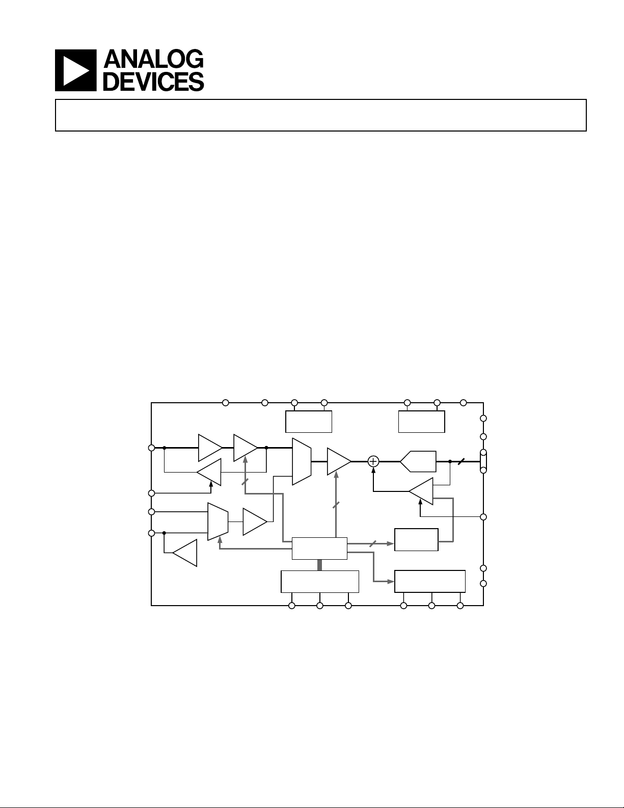
FUNCTIONAL BLOCK DIAGRAM
HD VD
CCDIN
CLPDM
AUX1IN
AUX2IN
CLP
AVDD
4dB 6dB
CDS
CLP
2:1
MUX
AD9845B
AVSS
PxGA
6
BUF
COLOR
STEERING
2:1
MUX
CONTROL
REGISTERS
DIGITAL
INTERFACE
GENERAL DESCRIPTION
The AD9845B is an improved version of the AD9845A CCD
signal processor. It features a 30 MHz single-channel architecture designed to sample and condition the outputs of interlaced
and progressive scan area CCD arrays. The AD9845B’s signal
chain consists of an input clamp, a correlated double sampler
(CDS), PxGA, a digitally controlled VGA, a black level clamp,
and a 12-bit A/D converter. Additional input modes are also
provided for processing analog video signals.
The internal registers are programmed through a 3-wire
serial digital interface. Programmable features include gain
adjustment, black level adjustment, input configuration, and
power-down modes.
The AD9845B operates from a single 3 V power supply, typically dissipates 153 mW, and is packaged in a 48-lead LQFP.
2dB~36dB
VGA
10
8
VRT VRB
BAND GAP
REFERENCE
ADC
CLP
BLK CLAMP
LEVEL
INTERNAL
TIMING
PBLK
12
DRVDD
DRVSS
DOUT
CLPOB
DVDD
DVSS
REV. A
Information furnished by Analog Devices is believed to be accurate and
reliable. However, no responsibility is assumed by Analog Devices for its
use, nor for any infringements of patents or other rights of third parties that
may result from its use. No license is granted by implication or otherwise
under any patent or patent rights of Analog Devices. Trademarks and
registered trademarks are the property of their respective companies.
SDATASCKSL
One Technology Way, P.O. Box 9106, Norwood, MA 02062-9106, U.S.A.
Tel: 781/329-4700 www.analog.com
Fax: 781/326-8703 © 2003 Analog Devices, Inc. All rights reserved.
SHDSHP
DATACLK

AD9845B–SPECIFICATIONS
(T
to T
GENERAL SPECIFICATIONS
MIN
, AVDD = DVDD = 3.0 V, f
MAX
Parameter Min Typ Max Unit
TEMPERATURE RANGE
Operating –20 +85 ∞C
Storage –65 +150 ∞C
POWER SUPPLY VOLTAGE
Analog, Digital, Digital Driver 2.7 3.6 V
POWER CONSUMPTION
Normal Operation (Specified under Each Mode of Operation)
Power-Down Modes
Standby 5 mW
Total Power-Down 0.5 mW
MAXIMUM CLOCK RATE 30 MHz
A/D CONVERTER
Resolution 12 Bits
Differential Nonlinearity (DNL) ± 0.5 ± 1.0 LSB
No Missing Codes 12 Bits Guaranteed
Full-Scale Input Voltage 2.0 V
Data Output Coding Straight Binary
VOLTAGE REFERENCE
Reference Top Voltage (VRT) 2.0 V
Reference Bottom Voltage (VRB) 1.0 V
Specifications subject to change without notice.
= 30 MHz, unless otherwise noted.)
DATACLK
DIGITAL SPECIFICATIONS
(DRVDD = 2.7 V, CL = 20 pF, unless otherwise noted.)
Parameter Symbol Min Typ Max Unit
LOGIC INPUTS
High Level Input Voltage V
Low Level Input Voltage V
High Level Input Current I
Low Level Input Current I
Input Capacitance C
IH
IL
IH
IL
IN
2.1 V
0.6 V
10 mA
10 mA
10 pF
LOGIC OUTPUTS
High Level Output Voltage, IOH = 2 mA V
Low Level Output Voltage, IOL = 2 mA V
Specifications subject to change without notice.
OH
OL
2.2 V
0.5 V
REV. A–2–

AD9845B
(T
to T
CCD MODE SPECIFICATIONS
MIN
, AVDD = DVDD = 3.0 V, f
MAX
Parameter Min Typ Max Unit Notes
P
OWER CONSUMPTION 153 mW See TPC 1 for Power Curves
MAXIMUM CLOCK RATE 30 MHz
CDS
Gain 0 dB
Allowable CCD Reset Transient
Max Input Range before Saturation
Max CCD Black Pixel Amplitude
1
1
1
1.0 V p-p PxGA Gain at 4 dB
500 mV
200 mV
PIXEL GAIN AMPLIFIER (PxGA)
Max Input Range 1.0 V p-p
Max Output Range 1.6 V p-p
Gain Control Resolution 64 Steps
Gain Monotonicity Guaranteed
Gain Range (Twos Complement Coding) See Figure 28 for PxGA
Min Gain (PxGA Gain Code 32) –2.5 dB
Max Gain (PxGA Gain Code 31) 9.5 dB
VARIABLE GAIN AMPLIFIER (VGA)
Max Input Range 1.6 V p-p
Max Output Range 2.0 V p-p
Gain Control Resolution 1024 Steps
Gain Monotonicity Guaranteed
Gain Range See Figure 29 for VGA Gain Curve
Low Gain (VGA Gain Code 77) 2 dB
Max Gain (VGA Gain Code 1023) 36 dB
BLACK LEVEL CLAMP
Clamp Level Resolution 256 Steps
Clamp Level Measured at ADC Output
Min Clamp Level 0 LSB
Max Clamp Level 255 LSB
SYSTEM PERFORMANCE Specifications Include Entire Signal Chain
Gain Accuracy
2
Low Gain (VGA Code 77) 5.5 6 6.5 dB
Max Gain (VGA Code 1023) 38.2 39.5 40.2 dB
Peak Nonlinearity, 500 mV Input Signal 0.1 % 12 dB Gain Applied
Total Output Noise 0.5 LSB rms AC Grounded Input, 6 dB Gain Applied
Power Supply Rejection (PSR) 40 dB Measured with Step Change on Supply
POWER-UP RECOVERY TIME Normal Clock Signals Applied
Reference Standby Mode 1 ms
Total Shutdown Mode 3 ms
Power-Off Condition 15 ms
NOTES
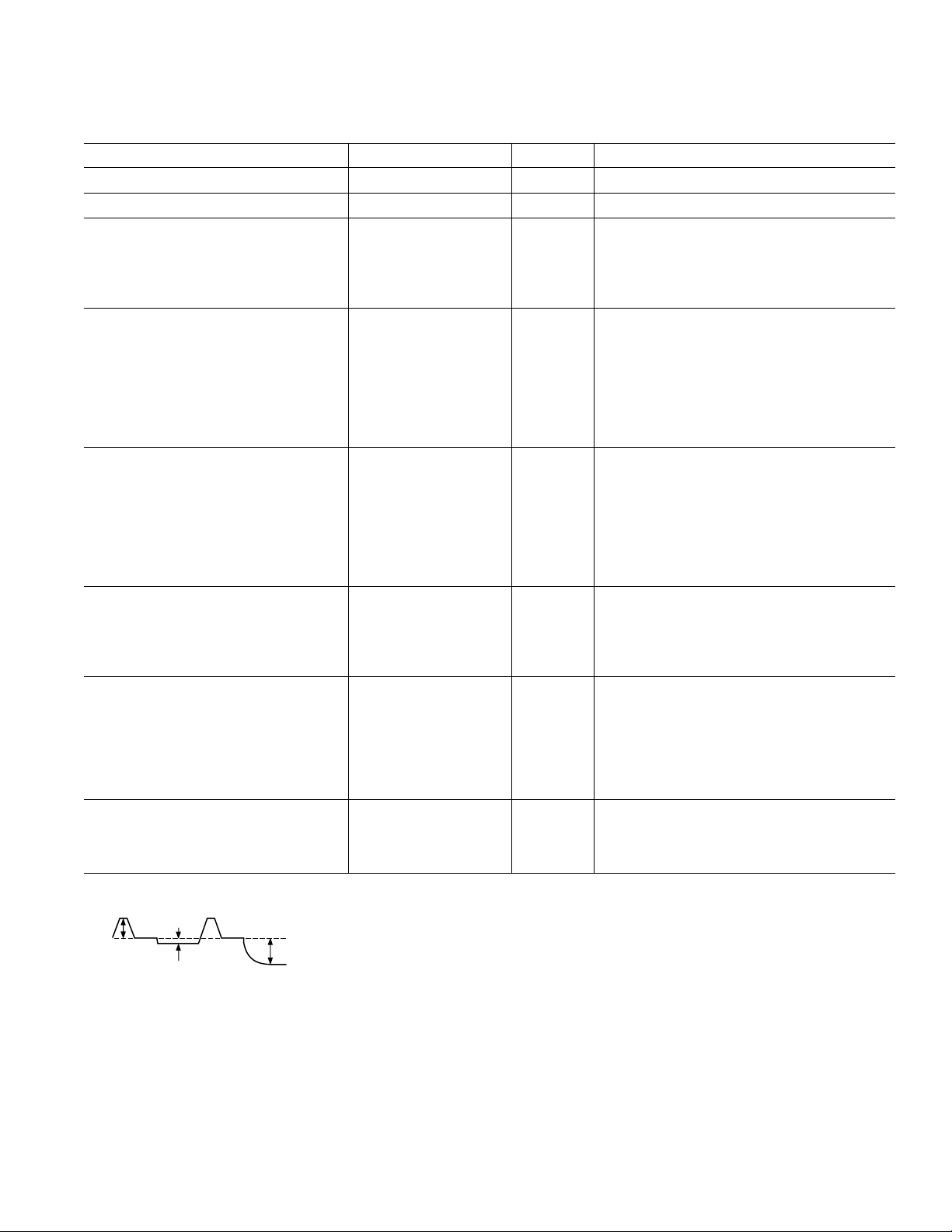
1
Input signal characteristics defined as follows:
DATACLK
= f
= f
SHP
= 30 MHz, unless otherwise noted.)
SHD
Gain = (0.0353 ⫻ Code) + 3.3
Gain Curve
500mV TYP
RESET TRANSIENT
2
PxGA gain fixed at Code 63 (3.3 dB).
Specifications subject to change without notice.
200mV MAX
OPTICAL BLACK PIXEL
1V MAX
INPUT SIGNAL RANGE
REV. A –3–

AD9845B
(T
to T
AUX1 MODE SPECIFICATIONS
Parameter Min Typ Max Unit
POWER CONSUMPTION 120 mW
MAXIMUM CLOCK RATE 30 MHz
INPUT BUFFER
Gain 0dB
Max Input Range 1.0 V p-p
VGA
Max Output Range 2.0 V p-p
Gain Control Resolution 1023 Steps
Gain (Selected Using VGA Gain Register)
Min Gain 0 dB
Max Gain 36 dB
Specifications subject to change without notice.
MIN
, AVDD = DVDD = 3.0 V, f
MAX
= 30 MHz, unless otherwise noted.)
DATACLK
AUX2 MODE SPECIFICATIONS
Parameter Min Typ Max Unit
POWER CONSUMPTION 120 mW
MAXIMUM CLOCK RATE 30 MHz
INPUT BUFFER (Same as AUX1 MODE)
VGA
Max Output Range 2.0 V p-p
Gain Control Resolution 512 Steps
Gain (Selected Using VGA Gain Register)
Min Gain 0 dB
Max Gain +18 dB
ACTIVE CLAMP
Clamp Level Resolution 256 Steps
Clamp Level (Measured at ADC Output)
Min Clamp Level 0 LSB
Max Clamp Level 255 LSB
Specifications subject to change without notice.
(T
to T
MIN
, AVDD = DVDD = 3.0 V, f
MAX
= 30 MHz, unless otherwise noted.)
DATACLK
REV. A–4–

AD9845B
TIMING SPECIFICATIONS
(CL = 20 pF, f
Serial Timing in Figures 21–24.)
= 30 MHz, CCD Mode Timing in Figures 5 and 6, AUX Mode Timing in Figure 7,
SAMP
Parameter Symbol Min Typ Max Unit
SAMPLE CLOCKS
DATACLK, SHP, SHD Clock Period t
DATACLK High/Low Pulsewidth t
SHP Pulsewidth t
SHD Pulsewidth t
CLPDM Pulsewidth t
CLPOB Pulsewidth
*
SHP Rising Edge to SHD Falling Edge t
SHP Rising Edge to SHD Rising Edge t
Internal Clock Delay t
Inhibited Clock Period t
CP
ADC
SHP
SHD
CDM
t
COB
S1
S2
ID
INH
33 33 ns
13 16.7 ns
5 8.3 ns
5 8.3 ns
410 Pixels
220 Pixels
0 8.3 ns
15 16.7 ns
3.0 ns
10 ns
DATA OUTPUTS
Output Delay t
Output Hold Time t
OD
H
7.0 7.6 ns
13 16 ns
Pipeline Delay 9 Cycles
SERIAL INTERFACE
Maximum SCK Frequency f
SL to SCK Setup Time t
SCK to SL Hold Time t
SDATA Valid to SCK Rising Edge Setup t
SCK Falling Edge to SDATA Valid Hold t
SCK Falling Edge to SDATA Valid Read t
*
Minimum CLPOB pulsewidth is for functional operation only. Wider typical pulses are recommended to achieve low noise clamp performance.
Specifications subject to change without notice.
SCLK
LS
LH
DS
DH
DV
10 MHz
10 ns
10 ns
10 ns
10 ns
10 ns
ABSOLUTE MAXIMUM RATINGS
With
Respect
Parameter To Min Max Unit
Model Range Description Option
AD9845BJST –20∞C to +85∞C LQFP ST-48
ORDERING GUIDE
Temperature Package Package
AVDD1, AVDD2 AVSS –0.3 +3.9 V
DVDD1, DVDD2 DVSS –0.3 +3.9 V
DRVDD DRVSS –0.3 +3.9 V
Digital Outputs DRVSS –0.3 DRVDD + 0.3 V
SHP, SHD, DATACLK DVSS –0.3 DVDD + 0.3 V
CLPOB, CLPDM, PBLK DVSS –0.3 DVDD + 0.3 V
SCK, SL, SDATA DVSS –0.3 DVDD + 0.3 V
THERMAL CHARACTERISTICS
Thermal Resistance
48-Lead LQFP Package
= 56∞C/W*
q
JA
*
q
is measured using a 4-layer PCB.
JA
VRT, VRB AVSS –0.3 AVDD + 0.3 V
BYP1-3, CCDIN AVSS –0.3 AVDD + 0.3 V
Junction Temperature 150 ∞C
Lead Temperature (10 sec) 300 ∞C
CAUTION
ESD (electrostatic discharge) sensitive device. Electrostatic charges as high as 4000 V readily
accumulate on the human body and test equipment and can discharge without detection. Although the
AD9845B features proprietary ESD protection circuitry, permanent damage may occur on devices
subjected to high energy electrostatic discharges. Therefore, proper ESD precautions are recommended
to avoid performance degradation or loss of functionality.
REV. A –5–

AD9845B
PIN CONFIGURATION
SCK
SDATASLSTBYNCDVSS
(LSB) D0
D1
D2
D3
D4
D5
D6
D7
D8
D9
D10
(MSB) D11
NC = NO CONNECT
48 47 46 4 5 44 39 38 3743 42 41 40
1
2
3
4
5
6
7
8
9
10
11
12
13 14 15 16 17 18 19 20 21 22 23 24
PIN 1
IDENTIFIER
DVSS
DRVSS
DRVDD
NC
AD9845B
TOP VIEW
(Not to Scale)
DVDD1
DATACLK
PIN FUNCTION DESCRIPTIONS
Pin Number Name Type Description
1–12 D0–D11 DO Digital Data Outputs. Pin 12 (D11) is MSB.
13 DRVDD P Digital Output Driver Supply
14 DRVSS P Digital Output Driver Ground
15, 41 DVSS P Digital Ground
16 DATACLK DI Digital Data Output Latch Clock
17 DVDD1 P Digital Supply 1
18 HD DI Horizontal Drive. Used with VD for color steering control.
19 PBLK DI Preblanking Clock Input
20 CLPOB DI Black Level Clamp Clock Input
21 SHP DI CDS Sampling Clock for CCD’s Reference Level
22 SHD DI CDS Sampling Clock for CCD’s Data Level
23 CLPDM DI Input Clamp Clock Input
24 VD DI Vertical Drive. Used with HD for color steering control.
25, 26, 35 AVSS P Analog Ground
27 AVDD1 P Analog Supply 1
28 BYP1 AO Internal Bias Level Decoupling
29 BYP2 AO Internal Bias Level Decoupling
30 CCDIN AI Analog Input for CCD Signal
31 NC NC Internally Not Connected
32 BYP3 AO Internal Bias Level Decoupling
33 AVDD2 P Analog Supply 2
34 AUX2IN AI Analog Input
36 AUX1IN AI Analog Input
37 NC NC Internally Not Connected
38 VRT AO A/D Converter Top Reference Voltage Decoupling
39 VRB AO A/D Converter Bottom Reference Voltage Decoupling
40 DVDD2 P Digital Supply 2
42 NC NC Internally Not Connected
43 NC NC Internally Not Connected
44 STBY DI Standby Mode, Active High. Same as total power-down mode.
45 NC NC Internally Not Connected
46 SL DI Serial Digital Interface Load Pulse
47 SDATA DI Serial Digital Interface Data
48 SCK DI Serial Digital Interface Clock
TYPE: AI = Analog Input, AO = Analog Output, DI = Digital Input, DO = Digital Output, P = Power
NC
HD
PBLK
DVDD2
SHP
CLPOB
VRB
SHD
VRT
NC
VD
CLPDM
36
35
34
33
32
31
30
29
28
27
26
25
AUX1IN
AVSS
AUX2IN
AVDD2
BYP3
NC
CCDIN
BYP2
BYP1
AVDD1
AVSS
AVSS
REV. A–6–

AD9845B
DEFINITIONS OF SPECIFICATIONS
Differential Nonlinearity (DNL)
An ideal ADC exhibits code transitions that are exactly 1 LSB
apart. DNL is the deviation from this ideal value. Thus, every code
must have a finite width. No missing codes guaranteed to 12-bit
resolution indicates that all 4096 codes, must be present over
all operating conditions.
Peak Nonlinearity
Peak nonlinearity, a full signal chain specification, refers to
the peak deviation of the output of the AD9845B from a true
straight line. The point used as “zero scale” occurs 1/2 LSB
before the first code transition. “Positive full scale” is defined as a
Level 1, 1/2 LSB beyond the last code transition. The deviation is
measured from the middle of each particular output code to the
true straight line. The error is then expressed as a percentage of the
2 V ADC full-scale signal. The input signal is always appropriately
gained up to fill the ADC’s full-scale range.
Total Output Noise
The rms output noise is measured using histogram techniques.
The standard deviation of the ADC output codes is calculated
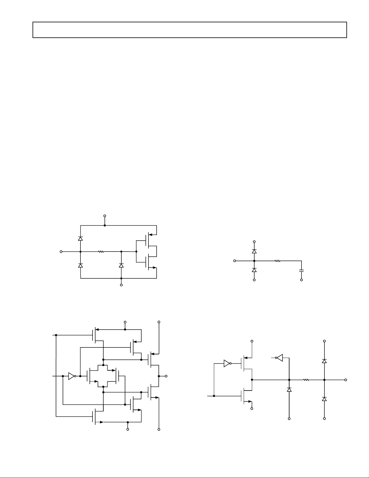
EQUIVALENT INPUT CIRCUITS
DVDD
in LSB and represents the rms noise level of the total signal
chain at the specified gain setting. The output noise can be
converted to an equivalent voltage using the relationship
N
1 LSB = (ADC Full Scale/2
codes)
where N is the bit resolution of the ADC. For the AD9845B,
1 LSB is approximately 488 mV.
Power Supply Rejection (PSR)
The PSR is measured with a step change applied to the supply
pins. This represents a high frequency disturbance on the
AD9845B’s power supply. The PSR specification is calculated
from the change in the data outputs for a given step change in
the supply voltage.
Internal Delay for SHP/SHD
The internal delay (also called aperture delay) is the time delay
that occurs from when a sampling edge is applied to the AD9845B
until the actual sample of the input signal is held. Both SHP and
SHD sample the input signal during the transition from low to
high, so the internal delay is measured from each clock’s rising
edge to the instant the actual internal sample is taken.
330
DVSS
Figure 1. Digital Inputs—SHP, SHD, DATACLK, CLPOB,
CLPDM, HD, VD, PBLK, SCK, and SL
DRVDD
DOUT
DATA
THREE-
STATE
DVDD
RNW
AVDD
AVSS
ACVSS
Figure 3. CCDIN (Pin 30)
DVDD
DATA IN
DATA OUT
DVSS
330
DVDD
REV. A
DVSS
Figure 2. Data Outputs—D0–D11
DRVSS
–7–
DVSS
Figure 4. SDATA (Pin 45)
DVSS

AD9845B–Typical Performance Characteristics
190
180
170
160
150
140
130
120
POWER DISSIPATION – mW
110
100
03020
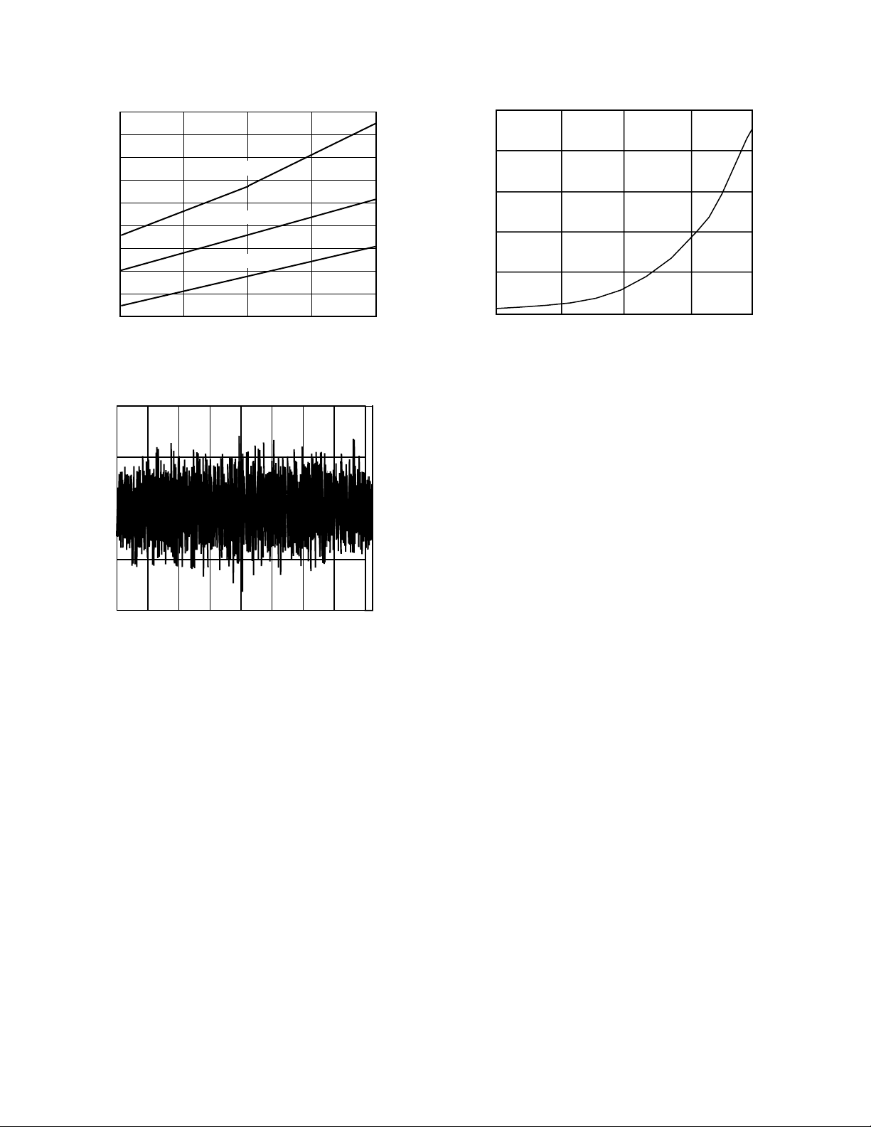
TPC 1. Power vs. Sample Rate
0.5
0.25
0
VDD = 3.3V
VDD = 3.0V
VDD = 2.7V
SAMPLE RATE – MHz
25
20
15
10
OUTPUT NOISE – LSB
5
0
0 1023511
255
VGA GAIN CODE – LSB
TPC 3. Output Noise vs. VGA Gain
767
–0.25
–0.5
0
500
1500 2000 2500 3000 3500 4000
1000
TPC 2. Typical DNL Performance
REV. A–8–
 Loading...