

Correlated Double Sampler (CDS)
FEATURES
40 MHz correlated double sampler (CDS)
Fixed 3.5 dB CDS gain
Low noise optical black clamp circuit
3 V single-supply operation
14-lead TSSOP package
APPLICATIONS
Digital still cameras
Digital video camcorders
CCTV cameras
PC cameras
Portable CCD imaging devices
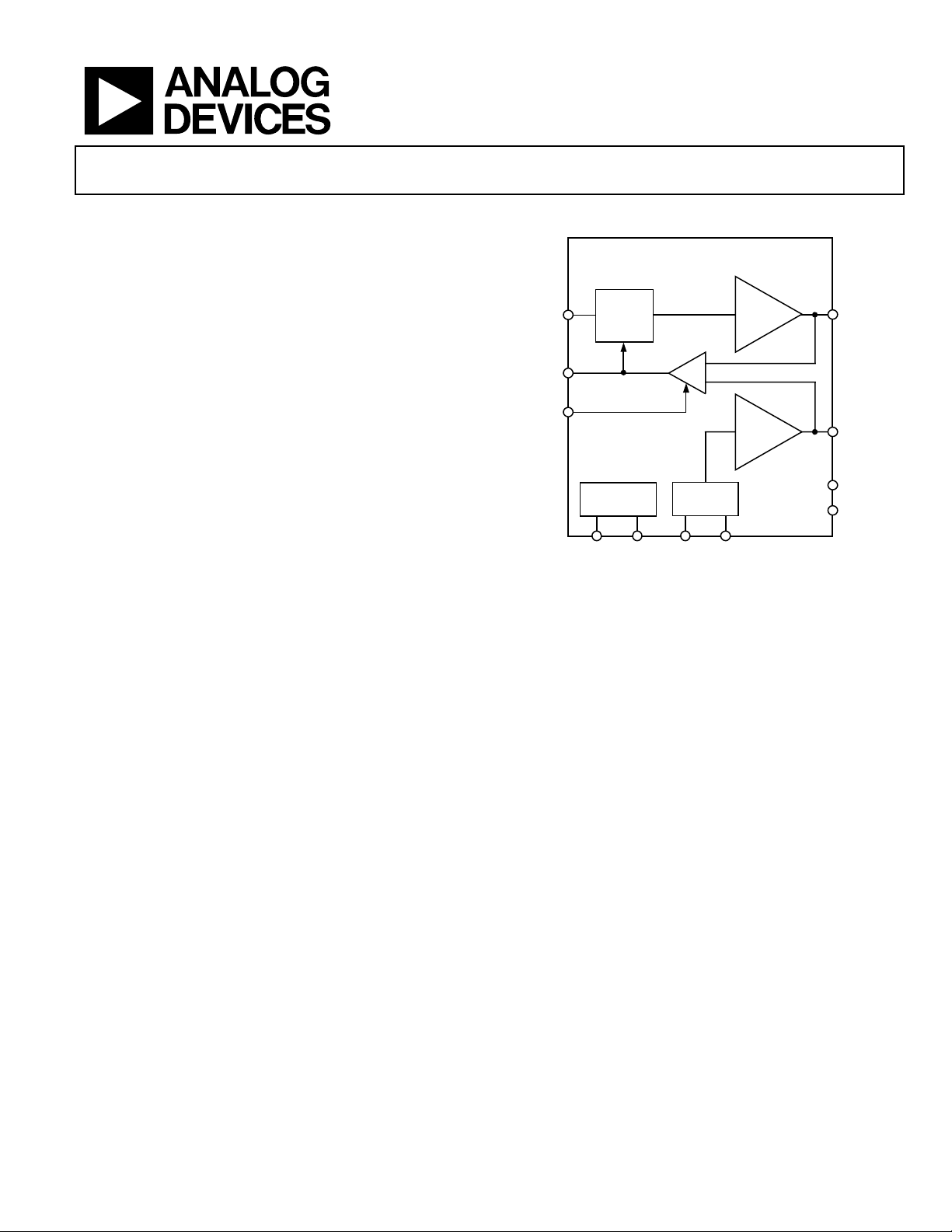
CCDIN
BYP2
CLP
AD9823
FUNCTIONAL BLOCK DIAGRAM
AD9823
3.5dB FIXED GAIN
CDS
CLP
INTERNAL
TIMING
SHDSHP
Figure 1. Functional Block Diagram
INTERNAL
REFERENCE
OUTPUT
BUFFER
OUTPUT
BUFFER
BYP3BYP1
OUTPUT
REFOUT
VDD
GND
04538-0-001
PRODUCT DESCRIPTION
The AD9823 is a correlated double sampler for digital camera
applications. It features a 40 MHz CDS amplifier with 3.5 dB of
fixed gain, an internal voltage reference supply, and timing
control for the SHP and SHD sampling clocks. Output buffers
are also included, providing drive strength for PCB traces and
direct connection to an image signal processor such as the
AD9821.
The AD9823 is ideal for applications that need to place the CDS
and VGA/ADC circuits on separate PC boards. The “pseudo
differential” outputs of the AD9823 provide good signal
integrity when interfaced with the differential input AD9821.
The AD9823 operates from a single 3 V power supply, typically
dissipates 50 mW, and is packaged in a 14-lead TSSOP package.
Rev. 0
Information furnished by Analog Devices is believed to be accurate and reliable.
However, no responsibility is assumed by Analog Devices for its use, nor for any
infringements of patents or other rights of third parties that may result from its use.
Specifications subject to change without notice. No license is granted by implication
or otherwise under any patent or patent rights of Analog Devices. Trademarks and
registered trademarks are the property of their respective owners.
One Technology Way, P.O. Box 9106, Norwood, MA 02062-9106, U.S.A.
Tel: 781.329.4700
Fax: 781.326.8703 © 2003 Analog Devices, Inc. All rights reserved.
www.analog.com

AD9823
TABLE OF CONTENTS
Specifications..................................................................................... 3
General Specifications ................................................................. 3
Analog Specifications................................................................... 3
Digital Specifications ................................................................... 3
Timing Specifications .................................................................. 4
Absolute Maximum Ratings............................................................ 5
REVISION HISTORY
Revision 0: Initial Version
Thermal Characteristics ...............................................................5
ESD Caution...................................................................................5
Pin Configuration and Function Descriptions..............................6
SHP and SHD Timing ..................................................................6
Outline Dimensions..........................................................................8
Ordering Guide .............................................................................8
Rev. 0 | Page 2 of 8
AD9823
T
SPECIFICATIONS
GENERAL SPECIFICATIONS
Table 1.
Parameter Min Typ Max Unit
Temperature Range
Operating –25 +85 °C
Storage –65 +150 °C
Power Supply Voltage 2.7 3.6 V
Power Consumption: f
Maximum Clock Rate 40 MHz
Minimum Clock Rate 5 MHz
ANALOG SPECIFICATIONS
Table 2. T
Parameter Min Typ Max Unit Notes
Analog Input (CCDIN)
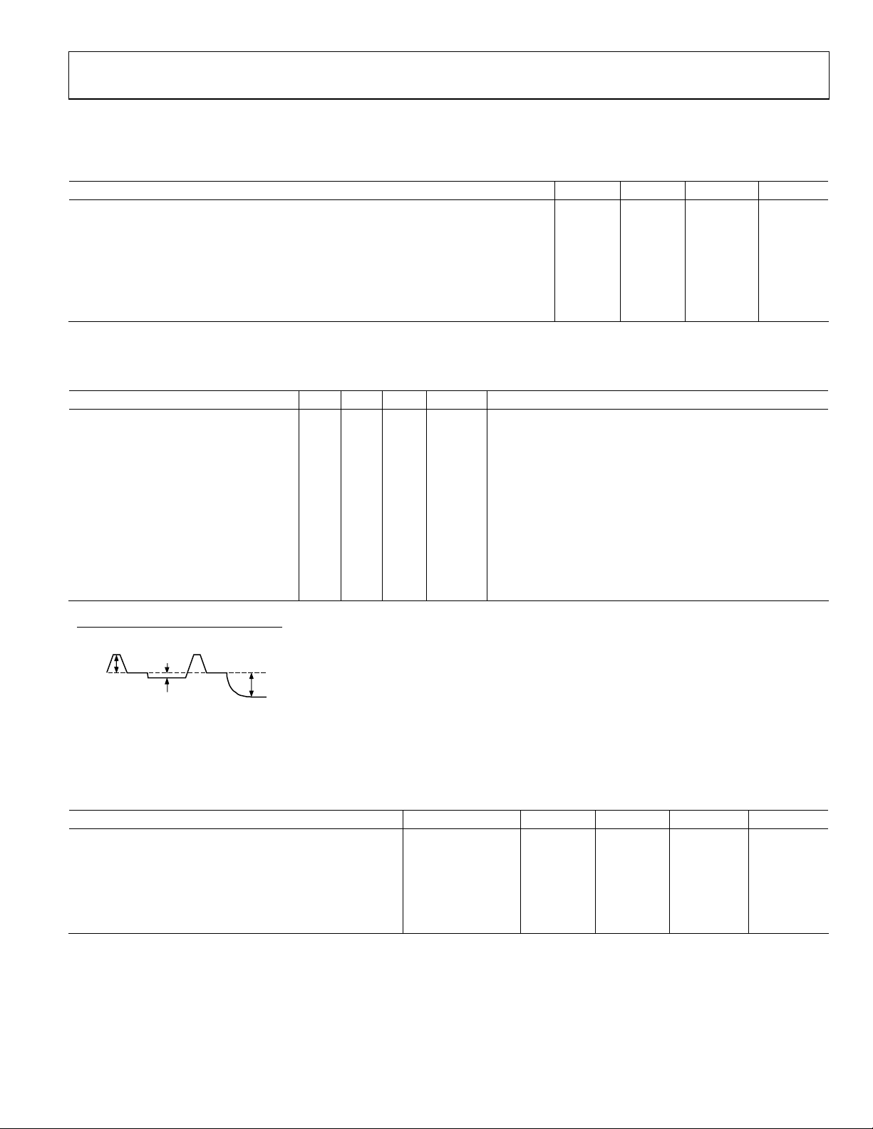
Max Input Range Before Saturation1 850 mV p-p
Allowable CCD Reset Transient1 500 mV
Max CCD Black Pixel Amplitude1 100 mV
Gain 2.5 3.5 4.5 dB
Nonlinearity, 500 mV Input 1.0 % Max deviation from ideal straight line
Input Referred Noise 100 µV rms Output noise divided by 3.5 dB gain
Clamp Time Constant 190 µsec 0.1 µF BYP2 capacitor (proportional to capacitor value)
Analog Outputs
Typical Data Out Signal Range 0.5 1.5 V 0.5 V corresponds to black level
REFOUT Voltage Level 0.5 V Fixed dc reference for signal output
1
Input signal characteristics defined as follows:
MIN
to T
= 40 MHz, VDD = 3.0 V 50 mW
SAMP
, VDD = 3.0 V, f
MAX
= 40 MHz, unless otherwise noted.
SAMP
500mV TYP
RESET TRANSIEN
All specifications subject to change without notice.
100mV TYP
OPTICAL BLACK PIXEL
850mV TYP
INPUT SIGNAL RANGE
04538-0-002
DIGITAL SPECIFICATIONS
Table 3.
Parameter Symbol Min Typ Max Unit
Logic Inputs (SHP, SHD, CLP)
High Level Input Voltage VIH 2.1 V
Low Level Input Voltage VIL 0.6 V
High Level Input Current IIH 10 µA
Low Level Input Current IIL 10 µA
Input Capacitance CIN 10 pF
Rev. 0 | Page 3 of 8

AD9823
TIMING SPECIFICATIONS
Table 4. T
Parameter (See Figure 3) Symbol Min Typ Max Unit
Sample Clocks
SHP, SHD Clock Period t
SHP Pulse Width t
SHD Pulse Width t
CLP Pulse Width
SHP Rising Edge to SHD Rising Edge t
SHD Rising Edge to SHP Rising Edge tS2 12.0 12.5 ns
Internal Clock Delay t
Recommended Data CLK Timing (for AD9821) t
1
Minimum CLP pulse width is for functional operation only. Wider typical pulses are recommended to achieve low noise clamp performance. Specifications subject to
change without notice.
MIN
to T
, VDD = 3.0 V, f
MAX
1
= 40 MHz, unless otherwise noted.
SAMP
CP
5 6.25 ns
SHP
SHD
t
COB
S1
ID
REC
25 ns
5 6.25 ns
4 10 pixels
12.0 12.5 ns
3.0 ns
4.5 ns
Rev. 0 | Page 4 of 8

AD9823
ABSOLUTE MAXIMUM RATINGS
Table 5.
Parameter With Respect To Min Max Unit
VDD GND −0.3 3.9 V
SHP, SHD GND −0.3 VDD + 0.3 V
BYP1, BYP2, BYP3 GND −0.3 VDD + 0.3 V
CCDIN GND −0.3 VDD + 0.3 V
DATAOUT, REFOUT GND −0.3 VDD + 0.3 V
CLP GND −0.3 VDD + 0.3 V
Junction Temperature 150 °C
Lead Temperature (10 sec) 350 °C
THERMAL CHARACTERISTICS
Thermal Resistance
14-Pin, TSSOP Package
= 89.2°C/W
θ
JA
ESD CAUTION
ESD (electrostatic discharge) sensitive device. Electrostatic charges as high as 4000 V readily accumulate on
the human body and test equipment and can discharge without detection. Although this product features
proprietary ESD protection circuitry, permanent damage may occur on devices subjected to high energy
electrostatic discharges. Therefore, proper ESD precautions are recommended to avoid performance
degradation or loss of functionality.
Rev. 0 | Page 5 of 8

AD9823
PIN CONFIGURATION AND FUNCTION DESCRIPTIONS
CLP
NC
VDD
REFOUT
DATAOUT
GND
BYP1
1
2
AD9823
3
TOP VIEW
4
(Not to Scale)
5
6
7
NC = NO CONNECT
14
13
12
11
10
9
8
SHP
SHD
GND
CCDIN
NC
BYP3
BYP2
04538-0-003
Figure 2. Pin Configurations
Table 6. Pin Function Descriptions
Pin Number Name Type
1
Description
1 CLP DI Input Clamp Clock Input (active low, not latched internally).
2 NC NC No connection should be connected to GND or VDD.
3 VDD P Analog Supply.
4 REFOUT AO Output Reference Level.
5 DATAOUT AO Output Data Signal.
6 GND P Analog Ground.
7 BYP1 AO Internal Bias Level Decoupling.
8 BYP2 AO Internal Bias Level Decoupling.
9 BYP3 AO Internal Bias Level Decoupling.
10 NC NC No connection should be connected to GND or VDD.
11 CCDIN AI CCD Input.
12 GND P Analog Ground.
13 SHD DI CDS Sampling Clock Input (For CCD Data Level).
14 SHP DI CDS Sampling Clock Input (For CCD Ref Level).
1
AI = Analog Input, AO = Analog Output, DI = Digital Input, DO = Digital Output, P = Power, NC = No Connect.
SHP AND SHD TIMING
CCD
SIGNAL
t
ID
SHP
SHD
DATAOUT
DATACLK
(FOR AD9821)
N N+1 N+2 N+9 N+10
t
t
SHD
t
REC
ID
t
SHPtS1
t
S2
t
CP
Figure 3. SHP and SHD Timing
Rev. 0 | Page 6 of 8
04538-0-004

AD9823
O
CCD
SIGNAL
CLP
EFFECTIVE PIXELS
(CONNECT TO VIN– ON AD9821)
(CONNECT TO VIN+ ON AD9821)
SERIAL
INTERFACE
3
OPTICAL BLACK PIXELS
4.7µF 0.1µF
CLP
REFOUT
DATAOUT
3V
ANALOG SUPPLY
HORIZONTAL
BLANKING
Figure 4. CLP Tim ing
3V
ANALOG
SUPPLY
CLP
1
NC
2
VDD
3
REFOUT
DATAOUT
GND
BYP1
0.1µF
AD9823
TOP VIEW
4
(Not to Scale)
5
6
7
NC = NO CONNECT
Figure 5. AD9823 Circuit Configuration
0.1µF
1.0µF
1.0µF
14
13
12
11
10
9
8
SHP
SHD
GND
CCDIN
NC
BYP3
BYP2
DUMMY PIXELS EFFECTIVE PIXELS
SHP
SHD
0.1µF
CCDIN
0.1µF0.1µF
04538-0-005
04538-0-007
DATA
UTPUTS
12
(MSB) D11
DRIVER
SUPPLY
SCK
SDATA
SLNCSTBY
DVSS
DVDD2
VRB
VRT
TEST
TEST
TEST
3
NC
3748 47 46 45 44 39 3843 42 41 40
NC
TEST
36
AVSS
35
TEST
34
AVDD2
33
BYP1
32
VIN–
31
VIN+
30
TEST
29
TEST
28
AVDD1
27
AVSS
26
AVSS
25
CLOCK
INPUTS
0.1µF
NC = INTERNALLY NOT CONNECTED
NC
D0
1
PIN 1
D1
2
IDENTIFIER
D2
3
D3
4
D4
5
D5
6
D6
7
D7
8
D8
9
D9
10
D10
11
12
13 14 15 16 17 18 19 20 21 22 23 24
DVSS
DRVSS
3V
DRVDD
0.1µF
0.1µF
ANALOG SUPPLY
AD9821
TOP VIEW
(Not to Scale
NC
DVDD1
DATACLK
3V
NC
PBLK
CLPOB
3V
ANALOG SUPPLY3VANALOG SUPPLY
0.1µF
0.1µF
IMAGER INPUT, NEGATIVE
IMAGER INPUT, POSITIVE
3V
ANALOG SUPPLY
4.7µF
4.7µF
0.1µF
CLP
NC
VDD
REFOUT
DATAOUT
GND
BYP1
0.1µF
1
2
3
AD9823
4
TOP VIEW
(Not to Scale)
5
6
7
14
13
12
11
10
9
8
SHP
SHD
GND
CCDIN
NC
BYP3
BYP2
0.1µF
0.1µF
0.1µF
CLP
SHP
SHD
OUTPUT
FROM
CCD
04538-0-006
Figure 6. Circuit Configuration with the AD9821 12-Bit Image Signal Processor
Rev. 0 | Page 7 of 8

AD9823
OUTLINE DIMENSIONS
5.10
5.00
4.90
1.05
1.00
0.80
4.50
4.40
4.30
PIN 1
14
0.65
BSC
0.15
0.05
COMPLIANT TO JEDEC STANDARDS MO-153AB-1
0.30
0.19
8
6.40
BSC
71
1.20
MAX
SEATING
PLANE
0.20
0.09
COPLANARITY
0.10
8°
0°
0.75
0.60
0.45
Figure 7. 14-Lead Thin Shrink Small Outline Package [ TSSOP]
(RU-14)
Dimensions shown in millimeters
ORDERING GUIDE
Model Temperature Range Package Description Package Option
AD9823BRUZ
1
Z = Pb-free part.
1
–25°C to +85°C TSSOP RU-14
© 2003 Analog Devices, Inc. All rights reserved. Trademarks and
registered trademarks are the property of their respective owners..
C04538-0-11/03(0)
Rev. 0 | Page 8 of 8
 Loading...