

16-Bit, 100 kSPS/200 kSPS
REF
V
ANA
4kV
R
D15
D0
DGND
BYTE
R/C
CS BUSY
V
DIG
V
IN
AGND2
CAP
AGND1
2.5V
REFERENCE
4R
CONTROL LOGIC &
INTERNAL CALIBRATION CIRCUITRY
CLOCK
PARALLEL
INTERFACE
SWITCHED
CAP ADC
AD976/AD976A
4R
3
R = 6kV AD976
R = 3kV AD976A
a
FEATURES
Fast 16-Bit ADC
200 kSPS Throughput – AD976A
100 kSPS Throughput – AD976
Single 5 V Supply Operation
Input Range: ⴞ10 V
100 mW Max Power Dissipation
Choice of External or Internal 2.5 V Reference
High Speed Parallel Interface
On-Chip Clock
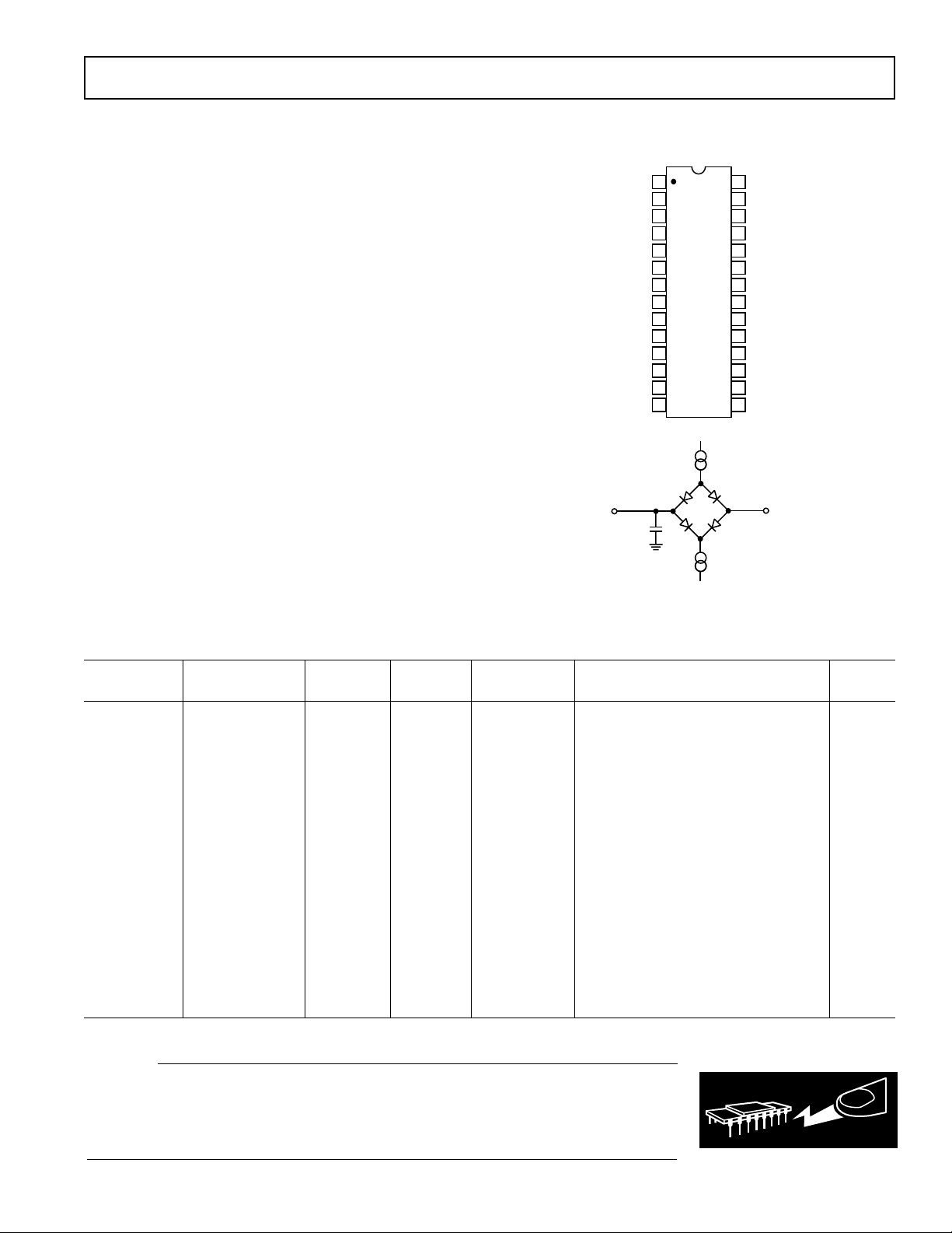
28-Lead Skinny DIP, SSOP or SOIC Packages
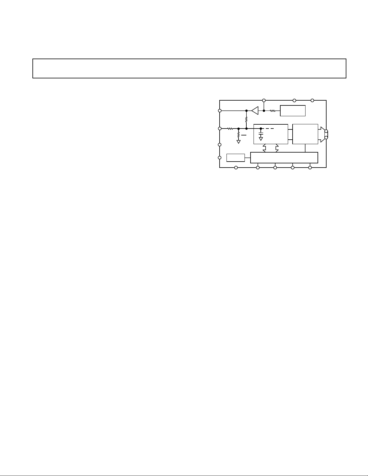
GENERAL DESCRIPTION
The AD976/AD976A is a high speed, low power 16-bit A/D
converter that operates from a single 5 V supply. The part contains a successive approximation, switched capacitor ADC, an
internal 2.5 V reference and a high speed parallel interface. The
ADC is factory calibrated to minimize all linearity errors. The
analog full-scale input is the standard industrial range of ±10 V.
The AD976/AD976A is comprehensively tested for ac parameters such as SNR and THD, as well as the more traditional
parameters of offset, gain and linearity.
The AD976/AD976A is fabricated on Analog Devices’ proprietary BiCMOS process, which has high performance bipolar
devices along with CMOS transistors.
The AD976/AD976A is available in skinny 28-lead DIP, SSOP
and SOIC packages.
BiCMOS A/D Converters
AD976/AD976A
FUNCTIONAL BLOCK DIAGRAM
PRODUCT HIGHLIGHTS
1. Fast Throughput.
The AD976/AD976A is a high speed (100 kSPS/200 kSPS
throughput rates respectively), 16-bit ADC based on a
switched capacitor architecture.
2. Single-Supply Operation.
The AD976/AD976A operates from a single 5 V supply and
dissipates only 100 mW max.
3. Comprehensive DC and AC Specifications.
The AD976/AD976A is factory calibrated and fully tested for
SNR and THD as well as the traditional specifications of
offset, gain and linearity.
4. Complete A/D Solution.
The AD976/AD976A offers a highly integrated solution
containing an accurate ADC, reference and on-chip clock.
REV. C
Information furnished by Analog Devices is believed to be accurate and
reliable. However, no responsibility is assumed by Analog Devices for its
use, nor for any infringements of patents or other rights of third parties
which may result from its use. No license is granted by implication or
otherwise under any patent or patent rights of Analog Devices.
One Technology Way, P.O. Box 9106, Norwood, MA 02062-9106, U.S.A.
Tel: 781/329-4700 World Wide Web Site: http://www.analog.com
Fax: 781/326-8703 © Analog Devices, Inc., 1999

AD976/AD976A
AD976A–SPECIFICATIONS
(–40ⴗC to +85ⴗC, FS = 200 kHz, Ref = Internal Reference, V
otherwise noted)
DIG
= V
ANA
= +5 V unless
Parameter Min Typ Max Min Typ Max Min Typ Max Units
AD976AA AD976AB AD976AC
RESOLUTION 16 16 16 Bits
ANALOG INPUT
Voltage Range ±10 ±10 ±10 V
Impedance 13 13 13 kΩ
Capacitance 22 22 22 pF
THROUGHPUT SPEED
Complete Cycle 5 5 5 µs
Throughput Rate 200 200 200 kHz
DC ACCURACY
Integral Linearity Error ±3 ±2 ±3 LSB
1
Differential Linearity Error –2 +3 –1 +1.75 ±2 LSB
No Missing Codes 15 16 15 Bit
Transition Noise
Full-Scale Error
3, 4
2
1.0 1.0 1.0 LSB
±0.5 ±0.25 ±0.5 %
Full-Scale Error Drift ±7 ±7 ±7 ppm/°C
Full-Scale Error, Ext. REF = 2.5 V ±0.5 ±0.25 ±0.5 %
Full-Scale Error Drift, Ext. REF = 2.5 V ±2 ±2 ±2 ppm/°C
Bipolar Zero Error
4
±10 ±10 ±15 mV
Bipolar Zero Error Drift ±2 ±2 ±2 ppm/°C
Power Supply Sensitivity
V
= V
= V
ANA
DIG
AC ACCURACY
Spurious Free Dynamic Range
Total Harmonic Distortion
Signal to (Noise + Distortion)
–60 dB Input 27 28 27 dB
Signal to Noise
Full-Power Bandwidth
= 5 V ± 5% ±8 ±8 ±8 LSB
D
5
5
5
5
7
90 96 90 dB
–90 –96 –90 dB
83 85 83 dB
83 85 83 dB
1 1 1 MHz
6
Input Bandwidth 2.7 2.7 2.7 MHz
SAMPLING DYNAMICS
Aperture Delay 40 40 40 ns
Transient Response
Full-Scale Step 1 1 1 µs
Overvoltage Recovery
8
150 150 150 ns
REFERENCE
Internal Reference Voltage 2.48 2.5 2.52 2.48 2.5 2.52 2.48 2.5 2.52 V
Internal Reference Source Current 1 1 1 µA
External Reference Voltage Range
for Specified Linearity 2.3 2.5 2.7 2.3 2.5 2.7 2.3 2.5 2.7 V
External Reference Current Drain
Ext. REF = 2.5 V 100 100 100 µA
DIGITAL INPUTS
Logic Levels
V
IL
V
IH
I
IL
I
IH
NOTES
1
LSB means least significant bit. With a ±10 V input, one LSB is 305 µV.
2
Typical rms noise at worst case transitions and temperatures.
3
Measured with fixed resistors as shown in Figure 5 (AD976) and Figure 6 (AD976A). Adjustable to zero as shown in Figure 7.
4
Full-scale error is expressed as the % difference between the actual full-scale code transition voltage and the ideal full-scale transition voltage and includes the effect
of offset error. The full-scale error is the worst case of either the –full-scale or +full-scale code transition voltage errors.
5
fIN = 20 kHz (AD976) and fIN = 45 kHz (AD976A), 0.5 dB down, unless otherwise noted.
6
All specifications in dB are referred to a full scale ±10 V input.
7
Full-power bandwidth is defined as full-scale input frequency at which signal-to-(noise + distortion) degrades to 60 dB or 10 bits of accuracy.
8
Recovers to specified performance after a 2 × F
Specifications subject to change without notice.
–0.3 +0.8 –0.3 +0.8 –0.3 +0.8 V
+2.0 V
+ 0.3 +2.0 V
DIG
+ 0.3 +2.0 V
DIG
+ 0.3 V
DIG
±10 ±10 ±10 µA
±10 ±10 ±10 µA
input overvoltage.
S
–2–
REV. C

AD976–SPECIFICATIONS
(–40ⴗC to +85ⴗC, FS = 100 kHz, Ref = Internal Reference,
V
= V
DIG
= +5 V unless otherwise noted)
ANA
AD976/AD976A
Parameter Min Typ Max Min Typ Max Min Typ Max Units
AD976A AD976B AD976C
RESOLUTION 16 16 16 Bits
ANALOG INPUT
Voltage Range ±10 ±10 ±10 V
Impedance 23 23 23 kΩ
Capacitance 22 22 22 pF
THROUGHPUT SPEED
Complete Cycle 10 10 10 µs
Throughput Rate 100 100 100 kHz
DC ACCURACY
Integral Linearity Error ±3 ±2 ±3 LSB
1
Differential Linearity Error –2 +3 –1 +1.75 ±2 LSB
No Missing Codes 15 16 15 Bit
Transition Noise
Full-Scale Error
3, 4
2
1.0 1.0 1.0 LSB
±0.5 ±0.25 ±0.5 %
Full-Scale Error Drift ±7 ±7 ±7 ppm/°C
Full-Scale Error, Ext. REF = 2.5 V ±0.5 ±0.25 ±0.5 %
Full-Scale Error Drift, Ext. REF = 2.5 V ±2 ±2 ±2 ppm/°C
Bipolar Zero Error
4
±10 ±10 ±15 mV
Bipolar Zero Error Drift ±2 ±2 ±2 ppm/°C
Power Supply Sensitivity
V
= V
= V
ANA
DIG
AC ACCURACY
Spurious Free Dynamic Range
Total Harmonic Distortion
Signal to (Noise + Distortion)
–60 dB Input 27 28 27 dB
Signal to Noise
Full-Power Bandwidth
= 5 V ± 5% ±8 ±8 ±8 LSB
D
5
5
5
5
7
90 96 90 dB
–90 –96 –90 dB
83 85 83 dB
83 85 83 dB
700 700 700 kHz
6
Input Bandwidth 1.5 1.5 1.5 MHz
SAMPLING DYNAMICS
Aperture Delay 40 40 40 ns
Transient Response
Full-Scale Step 2 2 2 µs
Overvoltage Recovery
8
150 150 150 ns
REFERENCE
Internal Reference Voltage 2.48 2.5 2.52 2.48 2.5 2.52 2.48 2.5 2.52 V
Internal Reference Source Current 1 1 1 µA
External Reference Voltage Range
for Specified Linearity 2.3 2.5 2.7 2.3 2.5 2.7 2.3 2.5 2.7 V
External Reference Current Drain
Ext. REF = 2.5 V 100 100 100 µA
DIGITAL INPUTS
Logic Levels
V
IL
V
IH
I
IL
I
IH
NOTES
1
LSB means least significant bit. With a ±10 V input, one LSB is 305 µV.
2
Typical rms noise at worst case transitions and temperatures.
3
Measured with fixed resistors as shown in Figure 5 (AD976) and Figure 6 (AD976A). Adjustable to zero as shown in Figure 7.
4
Full-scale error is expressed as the % difference between the actual full-scale code transition voltage and the ideal full-scale transition voltage and includes the effect
of offset error. The full-scale error is the worst case of either the –full-scale or +full-scale code transition voltage errors.
5
fIN = 20 kHz (AD976) and fIN = 45 kHz (AD976A), 0.5 dB down, unless otherwise noted.
6
All specifications in dB are referred to a full scale ±10 V input.
7
Full-power bandwidth is defined as full-scale input frequency at which signal-to-(noise + distortion) degrades to 60 dB or 10 bits of accuracy.
8
Recovers to specified performance after a 2 × F
Specifications subject to change without notice.
–0.3 +0.8 –0.3 +0.8 –0.3 +0.8 V
+2.0 V
+ 0.3 +2.0 V
DIG
+ 0.3 +2.0 V
DIG
+ 0.3 V
DIG
±10 ±10 ±10 µA
±10 ±10 ±10 µA
input overvoltage.
S
REV. C
–3–

AD976/AD976A
All Grades
Parameter Conditions Min Typ Max Units
DIGITAL OUTPUTS
Data Format Parallel 16 Bits
Data Coding Binary Twos Complement
V
OL
V
OH
Leakage Current High-Z State, ±5 µA
Output Capacitance High-Z State 15 pF
DIGITAL TIMING
Bus Access Time 83 ns
Bus Relinquish Time 83 ns
POWER SUPPLIES
Specified Performance
V
DIG
V
ANA
I
DIG
I
ANA
Power Dissipation 100 mW
TEMPERATURE RANGE
Specified Performance –40 +85 °C
I
= 1.6 mA +0.4 V
SINK
I
= 500 µA+4 V
SOURCE
V
= 0 V to V
OUT
DIG
4.75 5 5.25 V
4.75 5 5.25 V
3.0 mA
11 mA
Specifications subject to change without notice.
TIMING SPECIFICATIONS
(AD976A: FS = 200 kHz; AD976: FS = 100 kHz; –40ⴗC to +85ⴗC, V
Convert Pulsewidth t
Data Valid Delay after R/C Low (AD976A/AD976) t
BUSY Delay from R/C Low t
BUSY Low (AD976A/AD976) t
BUSY Delay after End of Conversion (AD976A/AD976) t
Aperture Delay t
Conversion Time (AD976A/AD976) t
Acquisition Time t
Bus Relinquish Time t
BUSY Delay after Data Valid (AD976A/AD976) t
Previous Data Valid after R/C Low (AD976A/AD976) t
Throughput Time (AD976A/AD976) t
R/C to CS Setup Time t
Time Between Conversions (AD976A/AD976) t
Bus Access and Byte Delay t
Specifications subject to change without notice.
= V
DIG
= +5 V unless otherwise noted)
ANA
Symbol Min Typ Max Units
1
2
3
4
5
6
7
8
9
10
11
+ t
7
12
13
14
8
50 ns
4.0/8.0 µs
83 ns
4.0/8.0 µs
180/360 ns
40 ns
3.8/7.6 4.0/8.0 µs
1.0/2.0 µs
10 35 83 ns
50 180/360 ns
3.7/7.4 µs
5/10 µs
10 ns
5/10 µs
10 83 ns
–4–
REV. C
AD976/AD976A
ABSOLUTE MAXIMUM RATINGS
1
Analog Inputs
V
. . . . . . . . . . . . . . . . . . . . . . . . . . . . . . . . . . . . . . . ±25 V
IN
CAP . . . . . . . . . . . . . . . . +V
+ 0.3 V to AGND2 – 0.3 V
ANA
REF . . . . . . . . . . . . . . . . . . . . . Indefinite Short to AGND2
Ground Voltage Differences
DGND, AGND1, AGND2 . . . . . . . . . . . . . . . . . . . . ±0.3 V
Supply Voltages
. . . . . . . . . . . . . . . . . . . . . . . . . . . . . . . . . . . . . . . . 7 V
V
ANA
to V
V
DIG
V
. . . . . . . . . . . . . . . . . . . . . . . . . . . . . . . . . . . . . . . . 7 V
DIG
Digital Inputs . . . . . . . . . . . . . . . . . . . –0.3 V to V
Internal Power Dissipation
. . . . . . . . . . . . . . . . . . . . . . . . . . . . . . . . ±7 V
ANA
2
DIG
+ 0.3 V
PDIP (N), SOIC (R), SSOP (RS) . . . . . . . . . . . . . 700 mW
Junction Temperature . . . . . . . . . . . . . . . . . . . . . . . . . +150°C
Storage Temperature Range (N, R, RS) . . . –65°C to +150°C
Lead Temperature Range
(Soldering 10 sec) . . . . . . . . . . . . . . . . . . . . . . . . . . +300°C
NOTES
1
Stresses above those listed under Absolute Maximum Ratings may cause perma-
nent damage to the device. This is a stress rating only; functional operation of the
device at these or any other conditions above those indicated in the operational
section of this specification is not implied. Exposure to absolute maximum rating
conditions for extended periods may affect device reliability.
2
Specification is for device in free air:
28-Lead PDIP: θJA = 74°C/W; θJC = 24°C/W,
28-Lead SOIC: θJA = 72°C/W; θJC = 23°C/W,
28-Lead SSOP: θJA = 109°C/W; θJC = 39°C/W.
PIN CONFIGURATION
DIP, SOIC and SSOP Packages
TO
OUTPUT
PIN
V
AGND1
REF
CAP
AGND2
D15 (MSB)
D14
D13
D12
D11
D10
DGND
C
100pF
IN
D9
D8
L
1
2
3
4
5
AD976A
6
TOP VIEW
(Not to Scale)
7
8
9
10
11
12
13
14
1.6mA I
500mA
AD976
28
27
26
25
24
23
22
21
20
19
18
17
16
15
OL
I
OH
V
DIG
V
ANA
BUSY
CS
R/C
BYTE
D0 (LSB)
D1
D2
D3
D4
D5
D6
D7
+2.1V
Figure 1. Load Circuit for Digital Interface Timing
ORDERING GUIDE
Temperature Max Min Throughput Package Package
Model Range INL S/(N+D) Rate Descriptions Options
AD976AN –40°C to +85°C ±3.0 LSB 83 dB 100 kSPS 28-Lead, 300 mil Plastic DIP N-28B
AD976BN –40°C to +85°C ±2.0 LSB 85 dB 100 kSPS 28-Lead, 300 mil Plastic DIP N-28B
AD976CN –40°C to +85°C 83 dB 100 kSPS 28-Lead, 300 mil Plastic DIP N-28B
AD976AAN –40°C to +85°C ±3.0 LSB 83 dB 200 kSPS 28-Lead, 300 mil Plastic DIP N-28B
AD976ABN –40°C to +85°C ±2.0 LSB 85 dB 200 kSPS 28-Lead, 300 mil Plastic DIP N-28B
AD976ACN –40°C to +85°C 83 dB 200 kSPS 28-Lead, 300 mil Plastic DIP N-28B
AD976AR –40°C to +85°C ±3.0 LSB 83 dB 100 kSPS 28-Lead Small Outline Package R-28
AD976BR –40°C to +85°C ±2.0 LSB 85 dB 100 kSPS 28-Lead Small Outline Package R-28
AD976CR –40°C to +85°C 83 dB 100 kSPS 28-Lead Small Outline Package R-28
AD976AAR –40°C to +85°C ±3.0 LSB 83 dB 200 kSPS 28-Lead Small Outline Package R-28
AD976ABR –40°C to +85°C ±2.0 LSB 85 dB 200 kSPS 28-Lead Small Outline Package R-28
AD976ACR –40°C to +85°C 83 dB 200 kSPS 28-Lead Small Outline Package R-28
AD976ARS –40°C to +85°C ±3.0 LSB 83 dB 100 kSPS 28-Lead Shrink Small Outline Package RS-28
AD976BRS –40°C to +85°C ±2.0 LSB 85 dB 100 kSPS 28-Lead Shrink Small Outline Package RS-28
AD976CRS –40°C to +85°C 83 dB 100 kSPS 28-Lead Shrink Small Outline Package RS-28
AD976AARS –40°C to +85°C ±3.0 LSB 83 dB 200 kSPS 28-Lead Shrink Small Outline Package RS-28
AD976ABRS –40°C to +85°C ±2.0 LSB 85 dB 200 kSPS 28-Lead Shrink Small Outline Package RS-28
AD976ACRS –40°C to +85°C 83 dB 200 kSPS 28-Lead Shrink Small Outline Package RS-28
CAUTION
ESD (electrostatic discharge) sensitive device. Electrostatic charges as high as 4000 V readily
accumulate on the human body and test equipment and can discharge without detection.
Although the AD976/AD976A features proprietary ESD protection circuitry, permanent damage
may occur on devices subjected to high energy electrostatic discharges. Therefore, proper ESD
precautions are recommended to avoid performance degradation or loss of functionality.
REV. C
–5–
WARNING!
ESD SENSITIVE DEVICE

AD976/AD976A
PIN FUNCTION DESCRIPTIONS
Pin No. Mnemonic Description
1V
IN
Analog Input. Connect a 200 Ω resistor between V
input range is ±10 V.
2 AGND1 Analog Ground. Used as the ground reference point for the REF pin.
3 REF Reference Input/Output. The internal +2.5 V reference is available at this pin. Alternatively, an
external reference can be used to override the internal reference. In either case, connect a 2.2 µF
tantalum capacitor between REF and AGND1.
4 CAP Reference Buffer Output. Connect a 2.2 µF tantalum capacitor between CAP and AGND2.
5 AGND2 Analog Ground.
6 D15 (MSB) Data Bit 15. Most significant bit of conversion result. High impedance state when CS is HIGH or
when R/C is LOW.
7–13 D14–D8 Data Bits 14–8. High impedance state when CS is HIGH or when R/C is LOW.
14 DGND Digital Ground.
15–21 D7–D1 Data Bits 7–1. High impedance state when CS is HIGH or when R/C is LOW.
22 D0 (LSB) Data Bit 0. Least significant bit of conversion result. High impedance state when CS is HIGH or
when R/C is LOW.
23 BYTE Byte Select. With BYTE LOW, data will be output as indicated above; Pin 6 (D15) is the MSB,
Pin 22 (D0) is the LSB. With BYTE HIGH, the top and bottom 8 bits of data will be switched;
D15–D8 are output on Pins 15–22 and D7–D0 are output on Pins 6–13.
24 R/C Read/Convert Input. With CS LOW, a falling edge on R/C puts the internal sample/hold into the
hold state and starts a conversion; a rising edge enables the output data bits.
25 CS Chip Select Input. Internally OR’d with R/C. With R/C LOW, a falling edge on CS will initiate a
conversion. With R/C HIGH, a falling edge on CS will enable the output data bits. When CS is
HIGH, the output data bits will be in the Hi-impedance state.
26 BUSY Busy Output. Goes LOW when a conversion is started and remains LOW until the conversion is
completed and the data is latched into the output register. With CS tied LOW and R/C HIGH,
output data will be valid when BUSY rises. The rising edge of BUSY can be used to latch the out-
put data.
27 V
28 V
ANA
DIG
Analog Power Supply. Nominally +5 V.
Digital Power Supply. Nominally +5 V.
and the analog signal source. The full-scale
IN
DEFINITION OF SPECIFICATIONS
INTEGRAL NONLINEARITY ERROR (INL)
Linearity error refers to the deviation of each individual code
from a line drawn from “negative full scale” to “positive full
scale.” The point used as negative full scale occurs 1/2 LSB
before the first code transition. Positive full scale is defined as a
level 1 1/2 LSB beyond the last code transition. The deviation is
measured from the middle of each particular code to the true
straight line.
DIFFERENTIAL NONLINEARITY ERROR (DNL)
In an ideal ADC, code transitions are 1 LSB apart. Differential
nonlinearity is the maximum deviation from this ideal value. It
is often specified in terms of resolution for which no missing
codes are guaranteed.
ⴞ FULL-SCALE ERROR
The last + transition (from 011. . .10 to 011. . .11) should
occur for an analog voltage 1 1/2 LSB below the nominal full
scale (9.9995422 V for a ±10 V range). The full-scale error is
the deviation of the actual level of the last transition from the
ideal level.
–6–
BIPOLAR ZERO ERROR
Bipolar zero error is the difference between the ideal midscale
input voltage (0 V) and the actual voltage producing the midscale
output code.
INPUT BANDWIDTH
The input bandwidth is that frequency at which the amplitude
of the reconstructed fundamental is reduced by 3 dB for a fullscale input.
FULL-POWER BANDWIDTH
Full-power bandwidth is defined as the full-scale input frequency at which signal to (Noise + Distortion) degrades to
60 dB, as 10 bits of accuracy.
APERTURE DELAY
Aperture delay is a measure of the Sample-and-Hold Amplifier
(SHA) performance and is measured from the rising edge of the
clock input to when the input signal is held for a conversion.
REV. C

AD976/AD976A
APERTURE JITTER
Aperture jitter is the variation in aperture delay for successive
samples and is manifested as noise on the input to the A/D.
TRANSIENT RESPONSE
The time required for the AD976/AD976A to achieve its rated
accuracy after a full-scale step function is applied to its input.
OVERVOLTAGE RECOVERY
The time required for the ADC to recover to full accuracy after
an analog input signal 150% of full-scale is reduced to 50% of
the full-scale value.
Signal-to-(Noise Plus Distortion Ratio) (S/[N+D])
S/(N+D) is the measured signal-to-noise plus distortion ratio at
the output of the ADC. The signal is the rms magnitude of the
fundamental. Noise plus distortion is the rms sum of all of the
nonfundamental signals and harmonics to half the sampling rate
excluding dc. The S/(N+D) is dependent upon the number of
quantization levels. The more levels, the lower the quantization
noise. The theoretical S/(N+D) for a sine wave input signal can
be calculated using the following:
S/(N+D) = (6.02N + 1.76) dB (1)
where N is the number of bits.
Thus, for an ideal 16 bit converter, S/(N+D) = 98 dB.
The output spectrum from the ADC is evaluated by applying a
low noise, low distortion sine wave signal to the V
pin and
IN
sampling at a 200 kHz throughput rate. By generating a Fast
Fourier Transform (FFT) plot, the S/(N+D) data can then be
obtained. Figure 10 shows a typical 2048-point FFT plot with
an input signal of 45 kHz and a sampling rate of 200 kHz. The
S/(N+D) obtained from this graph is 86.23 dB.
Since the measured S/(N+D) is less than the theoretical value, it
is possible to get a measure of performance expressed in effective
number of bits (ENOB).
ENOB = ((S/(N+D) – 1.76) / 6.02)
Thus for an input signal of 45 kHz, the typical ENOB is 14.
TOTAL HARMONIC DISTORTION (THD)
THD is the ratio of the rms sum of the harmonics to the rms
value of the fundamental. For the AD976/AD976A, THD is
defined as:
where V1 is the rms amplitude of the fundamental, and V2, V3,
, V5 and V6 are the rms amplitudes of the second through
V
4
sixth harmonics. The THD is also derived from the FFT plot of
the ADC output spectrum shown in Figure 10 and is seen there
as –105.33 dB.
Spurious Free Dynamic Range (SPFD)
The spurious free dynamic range is defined as the difference, in
dB, between the peak spurious or harmonic component in the
ADC output spectrum (up to F
/2 and excluding dc) and the rms
S
value of the fundamental. Normally, the value of this specification
will be determined by the largest harmonic in the spectrum. The
typical SPFD for the AD976/AD976A is –100 dB and can be
seen in Figure 10.
FUNCTIONAL DESCRIPTION
The AD976/AD976A is a high speed, low power, 16-bit sampling, analog-to-digital converter that can operate from a single
+5 volt power supply. The AD976/AD976A uses laser trimmed
scaling input resistors to provide an industry standard ±10 volt
input range. With a 100/200 kSPS throughput rate and a parallel interface, the AD976/AD976A is capable of connecting directly to digital signal processors and microcontrollers.
The AD976/AD976A employs a successive-approximation
technique to determine the value of the analog input voltage.
Instead of using the traditional laser-trimmed resistor-ladder
approach, however, this device uses a capacitor array charge
distribution technique. Binary weighted capacitors subdivide the
input sample to perform the actual analog-to-digital conversion.
The capacitor array eliminates variation in the linearity of the
device due to temperature-induced mismatches of resistor values. As a result of having an on-chip capacitor array, there is no
need for additional external circuitry to perform the sample/hold
function.
Initial errors in capacitor matching are eliminated at the time of
manufacturing. Calibration coefficients are calculated that correct for capacitor mismatches and are stored in on-chip thin-film
resistors that act as ROM. As a conversion is occurring, the appropriate calibration coefficients are read out of ROM. The accumulated coefficients are then used to adjust and improve conversion
accuracy. Any initial offset error is also trimmed out during
factory calibration. With the addition of an onboard reference
the AD976/AD976A provides a complete 16-bit A/D solution.
REV. C
THD dB
()
VVVVV
++++
=
20
223242526
log
V
1
2
–7–

AD976/AD976A
CONVERSION CONTROL
The AD976/AD976A is controlled by two signals: R/C and CS,
as shown in Figures 2 and 3. To initiate a conversion and place
the sample/hold circuit into the hold state, both the R/C and CS
signals must be brought low for no less than 50 ns. Once the
conversion process begins, the BUSY signal will go Low until
the conversion is complete. At the end of a conversion, BUSY
will return High, and the resulting valid data will be available on
the data bus. On the first conversion after the AD976/AD976A
is powered up, the DATA output will be indeterminate.
The AD976/AD976A exhibits two modes of conversion. In the
mode demonstrated in Figure 2, conversion timing is controlled
by a negative-going R/C signal, at least 50 ns wide. In this mode
the CS pin is always tied low, and the only limit placed on how
long the R/C signal can remain low is the desired sampling rate.
Less than 83 ns after the initiation of a conversion, the BUSY
signal will be brought low and remain low until the conversion is
complete and the output shift registers have been updated with
the new Binary Twos Complement data.
t
R/C
BUSY
MODE
DATA
BUS
ACQUIRE
PREVIOUS
DATA VALID
1
t
13
t
2
t
4
t
3
t
6
CONVERT CONVERTACQUIRE
t
7
t
14
t
11
PREVIOUS
DA TA VALID
HI-Z
t
9
Figure 2. Conversion Timing with Outputs Enabled After Conversion (CS Tied Low)
Figure 3 demonstrates the AD976/AD976A conversion timing,
using CS to control both the conversion process and the reading
of output data. To operate in this mode, the R/C signal should
be brought low no less than 10 ns before the falling edge of a CS
pulse (50 ns wide) is applied to the ADC. Once these two pulses
are applied, BUSY will go low and remain low until a conver-
sion is complete. After a maximum of 4 µs (AD976A only),
BUSY will again return high, and parallel data will be valid on
the ADC outputs. To achieve the maximum 100 kHz/200 kHz
throughput rate of the part, the negative going R/C and CS
control signals should be applied every 5 µs (AD976A). It should
also be noted that although all R/C and CS commands will be
ignored once a conversion has begun, these inputs can be
asserted during a conversion; i.e., a read during conversion can
be performed. Voltage transients on these inputs could feed
through to the analog circuitry and affect conversion results.
t
5
t
8
NOT
VALID
DATA
VALID
t
HI-Z
10
DATA
VALID
R/C
CS
BUSY
MODE
DATA
BUS
t
12
ACQUIRE
t
t
12
1
t
3
t
6
t
4
CONVERT ACQUIRE
t
7
HI-Z
t
12
t
1
DATA VALID
t
14
Figure 3. Using CS to Control Conversion and Read Timing
–8–
t
12
HI-Z
t
9
REV. C

AD976/AD976A
t
12
R/C
CS
BYTE
PINS 6–13
PINS 15–22
HI-Z
HI-Z
HIGH BYTE
t
14
LOW BYTE
Figure 4. Using CS and BYTE to Control Data Bus Read Timing
Regardless of the method for controlling conversions, output
data from conversion “n–1” will be valid during the BUSY Low
time for roughly 3.7 µs (AD976A only), and output data from
conversion “n” will be valid at the end of a conversion, 50 ns
) before BUSY returns High. It is recommended, however,
(t
10
that data is read only after BUSY goes high since this timing is
much more clearly defined and provides optimal performance.
Figure 4 demonstrates the functionality of the BYTE pin and
shows how the data will be valid in Binary Twos Complement
format only when R/C is asserted High and CS is Low. The
BYTE pin enables the output data on the bus to be read as a
full parallel output or as two 8-bit bytes on Pins 6–13 and Pins
15–22.
ANALOG INPUTS
Figure 5 shows the analog input section for the AD976 when
operating with an internal reference. The analog input range is
nominally a bipolar –10 V to +10 V. Since the AD976/AD976A
can be operated with an internal or external reference, the full-
scale analog input range can be best represented as ±4 V
REF
.
The nominal input impedance is 23 kΩ/13 kΩ with a 22 pF
input capacitance. The analog input section also has a ±25 V
overvoltage protection. Since the AD976/AD976A has two
analog grounds it is important to ensure that the analog input is
referenced to the AGND1 pin, the low current ground. This
will minimize any problems associated with a resistive ground
drop. It is also important to ensure that the analog input of the
AD976/AD976A is driven by a low impedance source. With its
primarily resistive analog input circuitry, the ADC can be driven
by a wide selection of general purpose amplifiers.
To best match the low distortion requirements of the AD976/
AD976A, care should be taken in the selection of the drive
circuitry op amp. Figure 6 shows the analog input section for
the AD976A when operating with an internal reference only.
Figure 9 shows the analog input section for both the AD976 and
the AD976A when operating with an external reference.
t
12
R1
200V
33.2kV
HI-Z
t
9
HI-Z
V
IN
R2
C1
2.2mF
C2
2.2mF
AGND1
AD976
REF
CAP
AGND2
LOW BYTE
t
14
HIGH BYTE
610V INPUT
Figure 5.±10 V Input Connection for the AD976 (Internal
Reference)
R1
+5V
200V
66.4kV
V
IN
R2
C1
2.2mF
C2
2.2mF
AGND1
AD976A
REF
V
ANA
CAP
AGND2
610V INPUT
Figure 6.±10 V Input Connection for the AD976A (Internal
Reference) Only
REV. C
–9–

AD976/AD976A
Table I. Offset and Gain Error for AD976
With Both External Without the External With the External 33.2K Without Either External
Error Term Resistors Included 33.2K Resistor Resistor Grounded Resistors Included
Offset Error –10 mV < Error < 10 mV –25 mV < Error < –5 mV –25 mV < Error < –5 mV –40 mV < Error < –15 mV
+Full Scale –0.50% < Error < 0.50%
Error –0.25% < Error < 0.25%
–Full Scale –0.50% < Error < 0.50%10.25% < Error < 1.25% –0.65% < Error < 0.35% –2.5% < Error < –1.0%
Error –0.25% < Error < 0.25%
With Both External Without the External With the External 33.2K Without Either External
Error Term Resistors Included 33.2K Resistor Resistor Grounded Resistors Included
Offset Error –10 mV < Error < 10 mV –25 mV < Error < –5 mV –25 mV < Error < –5 mV –55 mV < Error < –25 mV
+Full Scale –0.50% < Error < 0.50%
Error –0.25% < Error < 0.25%
–Full Scale –0.50% < Error < 0.50%10.25% < Error < 1.25% –0.65% < Error < 0.35% –3.50% < Error < –1.75%
Error –0.25% < Error < 0.25%
NOTES
1
For A grade part.
2
For B grade part.
1
–0.05% < Error < 0.95% –0.65% < Error < 0.35% 0.55% < Error < 1.90%
2
2
Table II. Offset and Gain Error for AD976A
1
–0.05% < Error < 0.95% –0.65% < Error < 0.35% 1.0% < Error < 2.50%
2
2
OFFSET AND GAIN ADJUSTMENT
The AD976/AD976A is factory trimmed to minimize gain,
offset and linearity errors. In some applications, where the analog input signal is required to meet the full dynamic range of the
ADC, the gain and offset errors need to be externally trimmed
to zero. Figure 7 shows the required trim circuitry to correct for
these offset and gain errors. Figure 8 shows the bipolar transfer
characteristic of the AD976/AD976A.
Where adjustment is required, offset error must be corrected
before gain error. To achieve this, trim the offset resistor R3
while the input voltage is 1/2 LSB below ground. By applying
a voltage of –152.6 µV at the input and adjusting the potentiom-
eter until the major carry transition is located between 1111
1111 1111 1111 and 0000 0000 0000 0000, the internal offset
can be corrected. To adjust the gain error, an analog signal
should be input at either the first code transition (ADC negative
full-scale) or the last code transition (ADC positive full-scale).
Thus, to adjust for full-scale error, an input voltage of 9.999542 V
(FS/2–3/2 LSBs) can be applied to the input and R4 should be
adjusted until the output code flickers between the last positive
code transition 0111 1111 1111 1111 and 0111 1111 1111 1110.
Should the first code transition need adjusting, the trim procedure
should consist of applying an analog input signal of –9.999847 V
(–FS/2 + 1/2 LSB) to the input and adjusting the trim until
the output code flickers between 1000 0000 0000 0000 and
1000 0000 0000 0001.
The external 200 Ω and 33.2K resistor shown in the data sheet for
the AD976 provide compensation for an internal adjustment of the
offset and gain which allows calibration with a single supply. These
resistors may not be required in some applications but it should be
noted that their removal will result in offset and gain errors in
addition to those listed in the electrical specifications of the data
sheet. Tables I and II illustrate the worst case range for Bipolar
Zero (offset) error and Full-Scale (gain) error for the AD976 and
the AD976A. All error terms are with respect to the A/D (i.e., a
negative offset in the table would have to be corrected with an
externally applied positive voltage).
610V
INPUT
33.2kV
R3
50kV
+5V
50kV
C1
2.2mF
R4
R5
576kV
C2
2.2mF
R2
V
IN
AGND1
AD976/
AD976A
REF
CAP
AGND2
R1
200V
Figure 7. Input Connection with Offset and Gain Adjustment
OUTPUT
CODE
011...111
011...110
(V
/2) – 1 LSB
REF
000...001
000...000
111...111
100...010
100...001
100...000
0V
(V
/2) + 1 LSB
REF
V
/2
V
= (AIN(+) - AIN(-)) – INPUT VOLTAGE
IN
REF
+ FS – 1 LSB
FS = V
REF
1LSB =
V
FS
65536
Figure 8. The Bipolar Transfer Characteristic of the
AD976/AD976A
–10–
REV. C

AD976/AD976A
FREQUENCY – kHz
0
–10
–150
0 10010 20 30 40
–40
–70
–130
–140
–20
–30
–60
–50
dB
–90
–120
–80
–110
–100
50 60 70 80 90 955 1525354555657585
F
SAMPLE
= 200kHz
F
IN
= 45kHz
SNR = 86.23dB
THD = –105.33dB
100%
VOLTAGE REFERENCE
The AD976/AD976A has an on-chip temperature compensated
bandgap voltage reference that is factory trimmed to 2.5 V
± 20 mV. The full-scale range of the ADC is equal to ±4V
Thus, the nominal range will be ±10 V.
The accuracy of the AD976 over the specified temperature
range is dominated by the drift performance of the voltage reference. The on-chip voltage reference is laser-trimmed to provide
a typical drift of 7 ppm/°C. This typical drift characteristic is
shown in Figure 13, which is a plot of the change in reference
voltage (in mV) versus the change in temperature—notice the
plot is normalized for zero error at +25°C. If improved drift
performance is required, an external reference such as the
AD780 should be used to provide a drift as low as 3 ppm/°C. In
order to simplify the drive requirements of the voltage reference
(internal or external), an onboard reference buffer is provided.
The output of this buffer is provided at the CAP pin and is
available to the user; however, when externally loading the reference buffer, it is important to make sure that proper precautions
are taken to minimize any degradation in the ADC’s performance. Figure 14 shows the load regulation of the reference
buffer. Notice that this figure is also normalized so that there is
zero error with no dc load. In the linear region, the output impedance at this point is typically 1 ohm. Because of this 1 ohm
output impedance, it is important to minimize any ac or input
dependent loads that will lead to increased distortion. Any dc
loads will simply act as a gain error. Although the typical characteristic of Figure 14 shows that the AD976 is capable of driving loads greater than 15 mA, it is not recommended that the
steady state current exceed 2 mA.
In addition to the on-chip reference, an external 2.5 V reference
can be applied. When choosing an external reference for a
16-bit application, however, careful attention should be paid to
noise and temperature drift. These critical specifications can
have a significant effect on the ADC performance.
Figure 9 shows the AD976/AD976A with the AD780 voltage
reference applied to the REF pin. The AD780 is a bandgap
reference that exhibits ultralow drift, low initial error, and low
output noise. For low power applications, the REF192 provides
a low quiescent current, high accuracy and low temperature
drift solution.
+5V
Figure 9. AD780 External Reference Connection to the
AD976/AD976A
REV. C
0.1mF
TEMP
AD780
V
IN
610V INPUT
V
OUT
GND
R1
200V
C3
1mF
R2
33.2kV
2.2mF
C4
0.1mF
2.2mF
AC PERFORMANCE
The AD976/AD976A is fully specified and tested for dynamic
performance specifications. The ac parameters are required for
.
REF
signal processing applications such as speech recognition and
spectrum analysis. These applications require information on
the ADC’s effect on the spectral content of the input signal.
Hence, the parameters for which the AD976/AD976A is
specified include: S/(N+D), THD and Spurious Free Dynamic
Range. These terms are discussed in greater detail in the following sections.
As a general rule, it is recommended that the results from several conversions be averaged to reduce the effects of noise, thus
improving parameters such as S/(N+D) and THD. The ac performance of the AD976/AD976A can be optimized by operating
the ADC at its maximum sampling rate of 100 kHz/200 kHz
and by digitally filtering the resulting bit stream to the desired
signal bandwidth. By distributing noise over a wider frequency
range, the noise density in the frequency band of interest can be
reduced. For example, if the required input bandwidth is 50 kHz,
the AD976A could be oversampled by a factor of 2. This would
yield a 3 dB improvement in the effective SNR performance.
Figure 10. FFT PLOT
DC PERFORMANCE
The factory calibration scheme used for the AD976/AD976A
compensates for bit weight errors that may exist in the capacitor
array. The mismatch in capacitor values is adjusted (using the
V
IN
REF
C1
AD976/
AD976A
AGND1
calibration coefficients) during a conversion, resulting in excellent
dc linearity performance. Figures 11, 12, 15, 16, 17 and 18,
respectively, show typical INL, typical DNL, typical positive and
negative INL and DNL distribution plots for the AD976/AD976A
at +25°C.
A histogram test is a statistical method for deriving an A/D
V
ANA
C2
CAP
AGND2
converter’s differential nonlinearity. A ramp input is sampled
by the ADC and a large number of conversions are taken and
stored. Theoretically, the codes would all be the same size and
therefore have an equal number of occurrences. A code with an
average number of occurrences would have a DNL of “0.” A
code that is different than the average would have a DNL that
was either greater or less than zero LSB. A DNL of –1 LSB
indicates that there is a missing code present at the 16-bit level
and that the ADC exhibits 15-bit performance.
–11–

AD976/AD976A
2.0
1.5
1.0
0.5
0
LSB
–0.5
–1.0
–1.5
–2.0
0665 101520253035
OUTPUT CODE – K
Figure 11. INL Plot
2.0
1.5
1.0
0.5
0
LSB
–0.5
–1.0
–1.5
–2.0
0
OUTPUT CODE – K
100%
40 45 50 55 60
100%
40 45 50 55 60
dV ON CAP PIN – 10mV/DIV
SOURCE CAPABILITY SINK CAPABILITY
LOAD CURRENT – 5mA/DIV
Figure 14. CAP (Pin 4) Load Regulation
90
80
70
60
50
40
30
NUMBER OF UNITS
20
10
0
665 101520253035
0
0.2
0.3
0.4
0.6
0.7
0.8
1.0
1.1
1.2
1.4
1.5
1.6
1.8
1.9
2.0
2.2
2.3
2.4
2.6
2.7
2.8
3.0
3.1
POSITIVE INL DISTRIBUTION – LSB
3.2
Figure 12. DNL Plot
1mV/DIV
–55
DEGREES CELSIUS
Figure 13. Reference Drift
25 125
Figure 15. Typical Positive INL Distribution (1516 Units)
90
80
70
60
50
40
30
NUMBER OF UNITS
20
10
0
–2.5
–2.4
–2.3
–2.2
–2.1
–2.0
–1.9
–1.8
–1.7
–1.6
–1.5
NEGATIVE INL DISTRIBUTION – LSB
–1.4
–1.3
–1.2
–1.1
–1.0
–0.9
–0.8
–0.7
–0.6
–0.5
–0.4
–0.3
–0.2
–0.1
Figure 16. Typical Negative INL Distribution (1516 Units)
–12–
REV. C

AD976/AD976A
ADDRESS BUS
*ADDITIONAL PINS OMITTED FOR CLARITY
DATA BUS
DB15
DB0
BUSY
AD976/
AD976A
R/C
BUS
74HC374
OE
Q15
Q0
D0
D15
CLK
EN
ADDR
DECODE
A0
A15
D15
D0
68000
R/W
AS
250
200
150
100
NUMBER OF UNITS
50
0
0
0.2
0.3
0.4
0.6
0.7
0.8
1.0
1.1
1.2
1.4
1.5
1.6
1.8
1.9
2.0
2.2
2.3
2.4
2.6
2.7
2.8
3.0
3.1
POSITIVE DNL DISTRIBUTION – LSB
3.2
Figure 17. Typical Position DNL Distribution (1516 Units)
DC CODE UNCERTAINTY
Ideally, a fixed dc input should result in the same output code
for repetitive conversions; however, as a consequence of unavoidable circuit noise within the wideband circuits of the ADC,
a range of output codes may occur for a given input voltage.
Thus, when a dc signal is applied to the AD976/AD976A input,
and 10,000 conversions are recorded, the result will be a distribution of codes as shown in Figure 19. This histogram shows a
bell-shaped curve consistent with the Gaussian nature of thermal noise. The histogram is approximately seven codes wide.
The standard deviation of this Gaussian distribution results in a
code transition noise of 1 LSB rms.
4000
3500
3000
2500
140
120
100
80
60
NUMBER OF UNITS
40
20
0
–1.2
–1
–1
–1.2
–1.1
–1.1
–0.9
–0.9
–0.8
–0.8
–0.7
NEGATIVE DNL DISTRIBUTION – LSB
–0.7
–0.6
–0.6
–0.5
–0.5
–0.4
–0.4
–0.3
–0.3
–0.2
–0.2
–0.1
–0.1
0
0
Figure 18. Typical Negative DNL Distribution (1516 Units)
MICROPROCESSOR INTERFACING
The AD976/AD976A is ideally suited for traditional dc measurement applications supporting a microprocessor and ac signal
processing applications interfacing to a digital signal processor.
The AD976/AD976A is designed to interface with a 16-bit data
bus and provides all output data bits in a single read cycle. A
variety of external buffers can be used with the AD976/AD976A
to prevent bus noise from coupling into the ADC. The following
sections illustrate the use of the AD976/AD976A with the
MC68000 and 8051 microcontrollers and the TMS320C25 and
ADSP-2111 signal processors.
MC68000 Interface
Figure 20 shows a general interface diagram for the MC68000
16-bit microprocessor to the AD976/AD976A. In Figure 20,
conversion is initiated by bringing CSA low (i.e., writing to the
appropriate address). This allows the processor to maintain
control over the complete conversion process.
2000
1500
1000
500
0
Figure 19. Histogram of 10,000 Conversions of a DC Input
REV. C
–2 –1 0 1 2 3 4
–3
Figure 20. AD976/AD976A to 68000 Interface
–13–

AD976/AD976A
8051 Interface
Figure 21 illustrates the use of the AD976/AD976A with an
8051 microcontroller.
P0
8051
P2
AD7
AD0
A15
A8
RD
WR
INT
BUS
LATCH
BUS
ADDR
BUS
DECODE
*ADDITIONAL PINS OMITTED FOR CLARITY
A0
DB7
DB0
AD976/
AD976A
BYTE
R/C
CS
BUSY
Figure 21. AD976/AD976A to 8051 Interface
TMS320C25 Interface
Figure 22 shows an interface between the AD976/AD976A and
the TMS320C25.
TIMER
A15
A0
TMS320C25
IS
READY
NSC
STRB
R/W
INT
D15
D0
ADDRESS BUS
ADDR
DECODE
EN
DATA BUS
*ADDITIONAL PINS OMITTED FOR CLARITY
R/C
CS
AD976A
BUSY
DB15
DB0
AD976/
Figure 22. AD976/AD976A to TMS320C25 Interface
ADSP-2111 Interface
Figure 23 shows an interface to the ADSP-2111 signal processor.
In this example, CS is being used to control conversions and is
generated by an external timer. A conversion is initiated each
time the timer output goes low as long as you are not reading
from the AD976/AD976A and while the Flag Output (FO) pin
of the ADSP-2111 is low. When a conversion is complete, the
BUSY line will return high. With the IRQn pin programmed to
generate an interrupt on a high-to-low transition, an interrupt
will occur at the end of each conversion. The 16-bit result of the
conversion can be read from within the interrupt service routine
by first forcing FO high, then performing a read operation with
the AD976/AD976A.
TIMER
A13
ADDRESS BUS
A0
ADSP-2111
DMS
RD
IRQn
FO
D15
D0
ADDR
DECODE
EN
DATA BUS
*ADDITIONAL PINS OMITTED FOR CLARITY
AD976A
CS
BUSY
R/C
DB15
DB0
AD976/
Figure 23. AD976/AD976A to ADSP-2111 Interface
POWER SUPPLIES AND DECOUPLING
The AD976/AD976A has two power supply input pins. V
and V
portions, respectively. V
analog circuitry, and V
provide the supply voltages to the analog and digital
DIG
is the +5 V supply for the on-chip
ANA
is the +5 V supply for the on-chip
DIG
ANA
digital circuitry. The AD976/AD976A is designed to be independent of power supply sequencing and, thus, free from supply
voltage induced latch-up.
With high performance linear circuits, changes in the power
supplies can result in undesired circuit performance. Optimally,
well regulated power supplies should be chosen with less than
1% ripple. The ac output impedance of a power supply is a
complex function of frequency and it will generally increase with
frequency. Thus, high frequency switching, such as that encountered with digital circuitry, requires the fast transient currents
that most power supplies can not adequately provide. Such a
situation results in large voltage spikes on the supplies. To compensate for the finite ac output impedance of most supplies,
charge “reserves” should be stored in bypass capacitors. This
will effectively lower the supplies impedance presented to the
AD976/AD976A V
ANA
and V
pins and reduce the magnitude
DIG
of these spikes. Decoupling capacitors, typically 0.1 µF, should
be placed close to the power supply pins of the AD976/AD976A
to minimize any inductance between the capacitors and the
V
ANA
and V
DIG
pins.
The AD976/AD976A may be operated from a single +5 V supply. When separate supplies are used, however, it is beneficial to
have larger capacitors, 10 µF, placed between the logic supply
(V
) and digital common (DGND) and between the analog
DIG
supply (V
) and the analog common (AGND2). Additionally,
ANA
10 µF capacitors should be located in the vicinity of the ADC to
further reduce low frequency ripple. In systems where the device
will be subjected to harsh environmental noise, additional decoupling may be required.
–14–
REV. C

AD976/AD976A
GROUNDING
The AD976/AD976A has three ground pins; AGND1, AGND2
and DGND. The analog ground pins are the “high quality”
ground reference points and should be connected to the system
analog common. AGND2 is the ground to which most internal
ADC analog signals are referenced. This ground is most
susceptible to current induced voltage drops and thus must be
connected with the least resistance back to the power supply.
AGND1 is the low current analog supply ground and should be
the analog common for the external reference, input op amp
drive circuitry and the input resistor divider circuit. By applying
the inputs referenced to this ground, any ground variations will
be offset and have a minimal effect on the resulting analog input
to the ADC. The digital ground pin, DGND, is the reference
point for all of the digital signals that control the AD976/AD976A.
The AD976/AD976A can be powered with two separate power
supplies or with a single analog supply. When the system digital
supply is noisy or fast switching digital signals are present, it is
recommended to connect the analog supply to both the V
and V
pins of the AD976/AD976A and the system supply to
DIG
ANA
the remaining digital circuitry. With this configuration, AGND1,
AGND2, and DGND should be connected back at the ADC.
When there is significant bus activity on the digital output pins,
the digital and analog supply pins on the ADC should be separated. This would eliminate any high speed digital noise from
coupling back to the analog portion of the AD976/AD976A.
In this configuration, the digital ground pin DGND should be
connected to the system digital ground and be separate from the
AGND pins.
BOARD LAYOUT
Designing with high resolution data converters requires careful
attention to board layout. Trace impedance is a significant issue.
A 1.22 mA current through a 0.5 Ω trace will develop a voltage
drop of 0.6 mV, which is 2 LSBs at the 16-bit level over the
20 volt full-scale range. Ground circuit impedances should be
reduced as much as possible since any ground potential differences between the signal source and the ADC appear as an error
voltage in series with the input signal. In addition to ground
drops, inductive and capacitive coupling needs to be considered.
This is especially true when high accuracy analog input signals
share the same board with digital signals. Thus, to minimize
input noise coupling, the input signal leads to V
and the signal
IN
return leads from AGND should be kept as short as possible. In
addition, power supplies should also be decoupled to filter out
ac noise.
Analog and digital signals should not share a common path.
Each signal should have an appropriate analog or digital return
routed close to it. Using this approach, signal loops enclose a
small area, minimizing the inductive coupling of noise. Wide PC
tracks, large gauge wire and ground planes are highly recommended to provide low impedance signal paths. Separate analog
and digital ground planes are also recommended with a single
interconnection point to minimize ground loops. Analog signals
should be routed as far as possible from high speed digital signals and should only cross them, if absolutely necessary, at right
angles.
In addition, it is recommended that multilayer PC boards be
used with separate power and ground planes. When designing
the separate sections, careful attention should be paid to the
layout.
REV. C
–15–

AD976/AD976A
OUTLINE DIMENSIONS
Dimensions shown in inches and (mm).
28-Lead 300 mil Plastic DIP
1.425 (36.195)
1.385 (35.179)
28
1
PIN 1
0.210 (5.33)
MAX
0.150 (3.81)
0.115 (2.92)
0.022 (0.558)
0.014 (0.356)
0.7125 (18.10)
0.6969 (17.70)
28 15
(N-28B)
0.100 (2.54)
BSC
28-Lead SOIC
(R-28)
15
14
0.015 (0.381)
0.070 (1.77)
0.045 (1.15)
0.280 (7.11)
0.240 (6.10)
MIN
SEATING
PLANE
0.325 (8.25)
0.300 (7.62)
0.014 (0.356)
0.008 (0.204)
0.195 (4.95)
0.115 (2.93)
C2624c–1–8/99
0.0118 (0.30)
0.0040 (0.10)
0.311 (7.9)
0.301 (7.64)
0.078 (1.98)
0.068 (1.73)
0.008 (0.203)
0.002 (0.050)
PIN 1
0.0500
(1.27)
BSC
0.0192 (0.49)
0.0138 (0.35)
SEATING
PLANE
28-Lead SSOP
(RS-28)
0.407 (10.34)
0.397 (10.08)
28 15
PIN 1
0.0256
(0.65)
BSC
0.015 (0.38)
0.010 (0.25)
SEATING
PLANE
0.2992 (7.60)
141
0.1043 (2.65)
0.0926 (2.35)
0.0125 (0.32)
0.0091 (0.23)
0.212 (5.38)
141
0.07 (1.79)
0.066 (1.67)
0.009 (0.229)
0.005 (0.127)
0.2914 (7.40)
0.4193 (10.65)
0.3937 (10.00)
0.205 (5.21)
8°
0°
0.0291 (0.74)
0.0098 (0.25)
0.0500 (1.27)
8°
0°
0.0157 (0.40)
0.03 (0.762)
0.022 (0.558)
x 45°
PRINTED IN U.S.A.
–16–
REV. C
 Loading...