Analog Devices AD9767 Datasheet
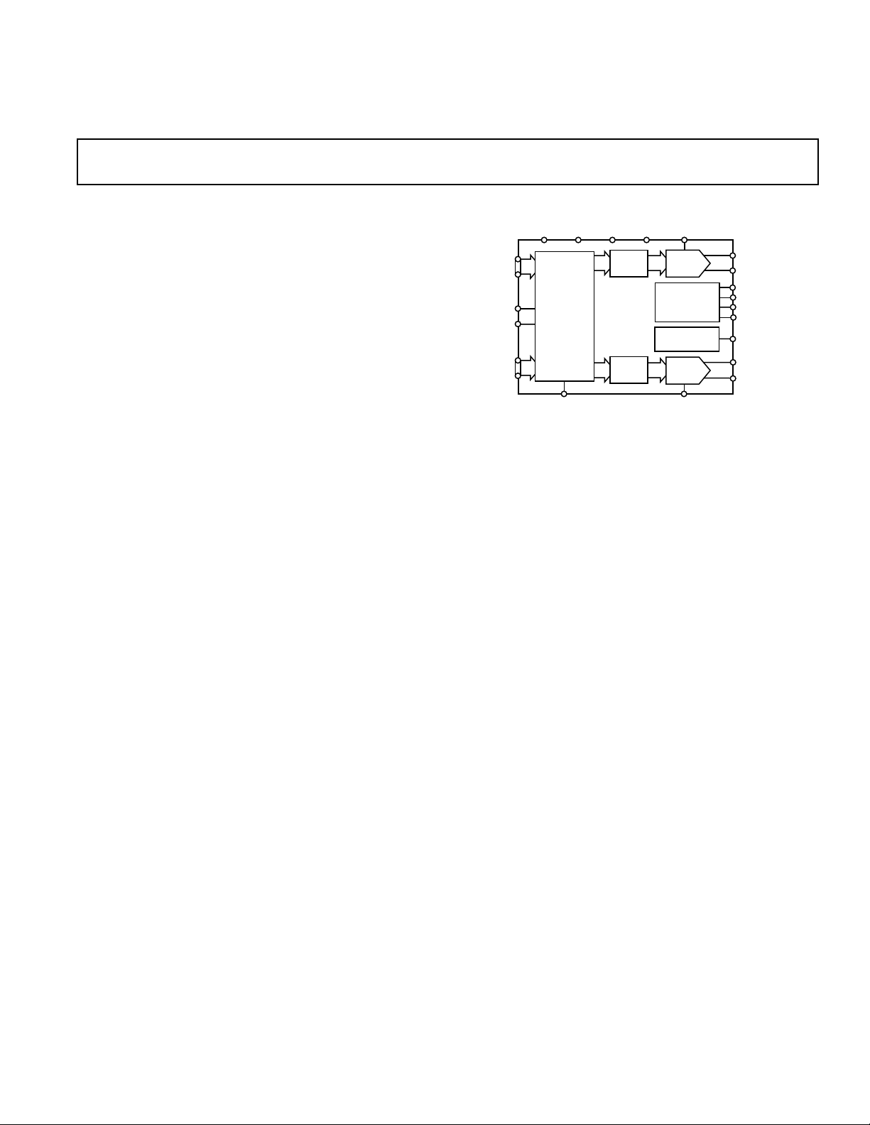
a
“1”
LATCH
“1”
DAC
REFIO
FSADJ1
FSADJ2
GAINCTRL
REFERENCE
BIAS
GENERATOR
I
OUTA1
I
OUTB1
SLEEP
I
OUTA2
I
OUTB2
DIGITAL
INTERFACE
AD9767
PORT1
PORT2
WRT1
WRT2
DVDD DCOM AVDD ACOM CLK1
CLK2
MODE
“2”
DAC
“2”
LATCH
14-Bit, 125 MSPS
Dual TxDAC+
®
D/A Converter
AD9767*
FEATURES
14-Bit Dual Transmit DAC
125 MSPS Update Rate
Excellent SFDR and IMD: 82 dBc
Excellent Gain and Offset Matching: 0.1%
Fully Independent or Single Resistor Gain Control
Dual Port or Interleaved Data
On-Chip 1.2 V Reference
Single 5 V or 3 V Supply Operation
Power Dissipation: 380 mW @ 5 V
Power-Down Mode: 50 mW @ 5 V
48-Lead LQFP
APPLICATIONS
Communications
Base Stations
Digital Synthesis
Quadrature Modulation
PRODUCT DESCRIPTION
The AD9767 is a dual port, high speed, two channel, 14-bit
CMOS DAC. It integrates two high quality 14-bit TxDAC+
cores, a voltage reference and digital interface circuitry into a small
48-lead LQFP package. The AD9767 offers exceptional ac and
dc performance while supporting update rates up to 125 MSPS.
The AD9767 has been optimized for processing I and Q data in
communications applications. The digital interface consists of
two double-buffered latches as well as control logic. Separate
write inputs allow data to be written to the two DAC ports
independent of one another. Separate clocks control the update
rate of the DACs.
A mode control pin allows the AD9767 to interface to two separate data ports, or to a single interleaved high speed data port.
In interleaving mode the input data stream is demuxed into its
original I and Q data and then latched. The I and Q data is then
converted by the two DACs and updated at half the input data
rate.
The GAINCTRL pin allows two modes for setting the full-scale
current (I
set independently using two external resistors, or I
) of the two DACs. I
OUTFS
for each DAC can be
OUTFS
OUTFS
for both
DACs can be set by using a single external resistor.**
The DACs utilize a segmented current source architecture combined with a proprietary switching technique to reduce glitch
energy and to maximize dynamic accuracy. Each DAC provides
FUNCTIONAL BLOCK DIAGRAM
differential current output thus supporting single-ended or
differential applications. Both DACs can be simultaneously
updated and provide a nominal full-scale current of 20 mA. The
full-scale currents between each DAC are matched to within
0.1%.
The AD9767 is manufactured on an advanced low cost CMOS
process. It operates from a single supply of 3.0 V to 5.0 V and
consumes 380 mW of power.
PRODUCT HIGHLIGHTS
1. The AD9767 is a member of a pin-compatible family of dual
TxDACs providing 8-, 10-, 12- and 14-bit resolution.
2. Dual 14-Bit, 125 MSPS DACs: A pair of high performance
DACs optimized for low distortion performance provide for
flexible transmission of I and Q information.
3. Matching: Gain matching is typically 0.1% of full scale, and
offset error is better than 0.02%.
4. Low Power: Complete CMOS Dual DAC function operates
on 380 mW from a 3.0 V to 5.0 V single supply. The DAC
full-scale current can be reduced for lower power operation,
and a sleep mode is provided for low power idle periods.
5. On-Chip Voltage Reference: The AD9767 includes a 1.20 V
temperature-compensated bandgap voltage reference.
6. Dual 14-Bit Inputs: The AD9767 features a flexible dualport interface allowing dual or interleaved input data.
TxDAC+ is a registered trademark of Analog Devices, Inc.
**Patent pending.
**Please see GAINCTRL Mode section, for important date code information on
this feature.
REV. B
Information furnished by Analog Devices is believed to be accurate and
reliable. However, no responsibility is assumed by Analog Devices for its
use, nor for any infringements of patents or other rights of third parties
which may result from its use. No license is granted by implication or
otherwise under any patent or patent rights of Analog Devices.
One Technology Way, P.O. Box 9106, Norwood, MA 02062-9106, U.S.A.
Tel: 781/329-4700 World Wide Web Site: http://www.analog.com
Fax: 781/326-8703 © Analog Devices, Inc., 2000

AD9767–SPECIFICATIONS
(T
to T
DC SPECIFICATIONS
MIN
, AVDD = +5 V, DVDD = +5 V, I
MAX
Parameter Min Typ Max Units
RESOLUTION 14 Bits
DC ACCURACY
1
Integral Linearity Error (INL)
T
= +25°C –3.5 ± 1.5 +3.5 LSB
A
T
MIN
to T
MAX
–4.0 +4.0 LSB
Differential Nonlinearity (DNL)
= +25°C –2.5 ± 1.0 +2.5 LSB
T
A
T
MIN
to T
MAX
–3.0 +3.0 LSB
ANALOG OUTPUT
Offset Error –0.02 +0.02 % of FSR
Gain Error (Without Internal Reference) –2 ±0.25 +2 % of FSR
Gain Error (With Internal Reference) –5 ±1 +5 % of FSR
Gain Match –1.6 0.1 +1.6 % of FSR
–0.14 +0.14 dB
2.0 20.0 mA
Full-Scale Output Current
2
Output Compliance Range –1.0 +1.25 V
Output Resistance 100 kΩ
Output Capacitance 5 pF
REFERENCE OUTPUT
Reference Voltage 1.14 1.20 1.26 V
Reference Output Current
3
REFERENCE INPUT
Input Compliance Range 0.1 1.25 V
Reference Input Resistance 1 MΩ
Small Signal Bandwidth 0.5 MHz
TEMPERATURE COEFFICIENTS
Offset Drift 0 ppm of FSR/°C
Gain Drift (Without Internal Reference) ±50 ppm of FSR/°C
Gain Drift (With Internal Reference) ±100 ppm of FSR/°C
Reference Voltage Drift ±50 ppm/°C
POWER SUPPLY
Supply Voltages
AVDD 3 5 5.5 V
DVDD 2.7 5 5.5 V
Analog Supply Current (I
Digital Supply Current (I
Digital Supply Current (I
Supply Current Sleep Mode (I
Power Dissipation
Power Dissipation
Power Dissipation
4
(5 V, I
5
(5 V, I
6
(5 V, I
Power Supply Rejection Ratio
)7175mA
AVDD
4
)
DVDD
5
)
DVDD
OUTFS
OUTFS
OUTFS
)812mA
AVDD
= 20 mA) 380 410 mW
= 20 mA) 420 450 mW
= 20 mA) 450 mW
7
—AVDD –0.4 +0.4 % of FSR/V
Power Supply Rejection Ratio7—DVDD –0.025 +0.025 % of FSR/V
OPERATING RANGE –40 +85 °C
NOTES
1
Measured at I
2
Nominal full-scale current, I
3
An external buffer amplifier with input bias current <100 nA should be used to drive any external load.
4
Measured at f
5
Measured at f
6
Measured as unbuffered voltage output with I
7
±10% Power supply variation.
Specifications subject to change without notice.
, driving a virtual ground.
OUTA
= 25 MSPS and f
CLOCK
= 100 MSPS and f
CLOCK
, is 32 times the I
OUTFS
= 1.0 MHz.
OUT
= 1 MHz.
OUT
current.
REF
= 20 mA and 50 Ω R
OUTFS
LOAD
at I
OUTA
= 20 mA, unless otherwise noted.)
OUTFS
100 nA
57 mA
15 mA
and I
OUTB
, f
= 100 MSPS and f
CLOCK
= 40 MHz.
OUT
–2–
REV. B

AD9767
(T
to T
DYNAMIC SPECIFICATIONS
MIN
, AVDD = +5 V, DVDD = +5 V, I
MAX
Output, 50 ⍀ Doubly Terminated, unless otherwise noted)
Parameter Min Typ Max Units
DYNAMIC PERFORMANCE
Maximum Output Update Rate (f
Output Settling Time (t
Output Propagation Delay (t
) (to 0.1%)
ST
)1ns
PD
Glitch Impulse 5 pV-s
Output Rise Time (10% to 90%)
Output Fall Time (90% to 10%)
Output Noise (I
Output Noise (I
= 20 mA) 50 pA/√Hz
OUTFS
= 2 mA) 30 pA/√Hz
OUTFS
) 125 MSPS
CLOCK
1
1
1
AC LINEARITY
Spurious-Free Dynamic Range to Nyquist
= 100 MSPS; f
f
CLOCK
= 1.00 MHz
OUT
0 dBFS Output 71 82 dBc
–6 dBFS Output 77 dBc
–12 dBFS Output 73 dBc
–18 dBFS Output 70 dBc
= 65 MSPS; f
f
CLOCK
= 65 MSPS; f
f
CLOCK
f
= 65 MSPS; f
CLOCK
f
= 65 MSPS; f
CLOCK
= 65 MSPS; f
f
CLOCK
f
= 125 MSPS; f
CLOCK
f
= 125 MSPS; f
CLOCK
= 1.00 MHz 82 dBc
OUT
= 2.51 MHz 80 dBc
OUT
= 5.02 MHz 79 dBc
OUT
= 14.02 MHz 70 dBc
OUT
= 25 MHz 55 dBc
OUT
= 25 MHz 67 dBc
OUT
= 40 MHz 70 dBc
OUT
Spurious-Free Dynamic Range Within a Window
= 100 MSPS; f
f
CLOCK
f
= 50 MSPS; f
CLOCK
= 65 MSPS; f
f
CLOCK
f
= 125 MSPS; f
CLOCK
= 1.00 MHz; 2 MHz Span 82 91 dBc
OUT
= 5.02 MHz; 10 MHz Span 88 dBc
OUT
= 5.03 MHz; 10 MHz Span 88 dBc
OUT
= 5.04 MHz; 10 MHz Span 88 dBc
OUT
Total Harmonic Distortion
= 100 MSPS; f
f
CLOCK
f
= 50 MSPS; f
CLOCK
f
= 125 MSPS; f
CLOCK
= 125 MSPS; f
f
CLOCK
= 1.00 MHz –81 –71 dBc
OUT
= 2.00 MHz –79 dBc
OUT
= 4.00 MHz –83 dBc
OUT
= 10.00 MHz –80 dBc
OUT
Multitone Power Ratio (Eight Tones at 110 kHz Spacing)
f
= 65 MSPS; f
CLOCK
= 2.00 MHz to 2.99 MHz
OUT
0 dBFS Output 80 dBc
–6 dBFS Output 79 dBc
–12 dBFS Output 78 dBc
–18 dBFS Output 76 dBc
Channel Isolation
= 125 MSPS; f
f
CLOCK
f
= 125 MSPS; f
CLOCK
NOTES
1
Measured single-ended into 50 Ω load.
Specifications subject to change without notice.
= 10 MHz 85 dBc
OUT
= 40 MHz 77 dBc
OUT
= 20 mA, Differential Transformer Coupled
OUTFS
35 ns
2.5 ns
2.5 ns
REV. B –3–
AD9767–SPECIFICATIONS
WARNING!
ESD SENSITIVE DEVICE
(T
to T
DIGITAL SPECIFICATIONS
MIN
, AVDD = +5 V, DVDD = +5 V, I
MAX
Parameter Min Typ Max Units
DIGITAL INPUTS
Logic “1” Voltage @ DVDD = +5 V 3.5 5 V
Logic “1” @ DVDD = 3 2.1 3 V
Logic “0” Voltage @ DVDD = +5 V 0 1.3 V
Logic “0” @ DVDD = 3 0 0.9 V
Logic “1” Current –10 +10 µA
Logic “0” Current –10 +10 µA
Input Capacitance 5 pF
Input Setup Time (t
Input Hold Time (t
Latch Pulsewidth (t
Specifications subject to change without notice.
) 2.0 ns
S
) 1.5 ns
H
, t
LPW
) 3.5 ns
CPW
ABSOLUTE MAXIMUM RATINGS*
With
Parameter Respect to Min Max Units
AVDD ACOM –0.3 +6.5 V
DVDD DCOM –0.3 +6.5 V
ACOM DCOM –0.3 +0.3 V
AVDD DVDD –6.5 +6.5 V
MODE, CLK1, CLK2, WRT1, WRT2 DCOM –0.3 DVDD + 0.3 V
Digital Inputs DCOM –0.3 DVDD + 0.3 V
I
OUTA1/IOUTA2
, I
OUTB1/IOUTB2
ACOM –1.0 AVDD + 0.3 V
REFIO, FSADJ1, FSADJ2 ACOM –0.3 AVDD + 0.3 V
GAINCTRL, SLEEP ACOM –0.3 AVDD + 0.3 V
Junction Temperature +150 °C
Storage Temperature –65 +150 °C
Lead Temperature (10 sec) +300 °C
*Stresses above those listed under Absolute Maximum Ratings may cause permanent damage to the device. This is a stress rating only; functional operation of the
device at these or any other conditions above those indicated in the operational sections of this specification is not implied. Exposure to absolute maximum ratings for
extended periods may affect device reliability.
= 20 mA, unless otherwise noted.)
OUTFS
ORDERING GUIDE
Temperature Package Package
Model Range Description Option*
(WRT2) (WRT1 / IQWRT)
DATA IN
AD9767AST –40°C to +85°C 48-Lead LQFP ST-48
AD9767-EB Evaluation Board
*ST = Thin Plastic Quad Flatpack.
(CLK2) (CLK1/ IQCLK)
THERMAL CHARACTERISTICS
Thermal Resistance
48-Lead LQFP
θ
= 91°C/W
JA
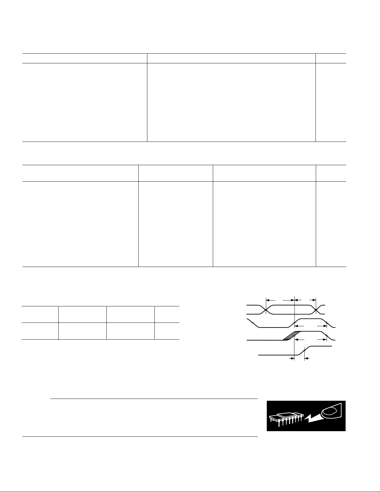
Figure 1. Timing Diagram for Dual and Interleaved Modes
See Dynamic and Digital sections for timing specifications.
CAUTION
ESD (electrostatic discharge) sensitive device. Electrostatic charges as high as 4000 V readily
accumulate on the human body and test equipment and can discharge without detection.
Although the AD9767 features proprietary ESD protection circuitry, permanent damage may
occur on devices subjected to high energy electrostatic discharges. Therefore, proper ESD
precautions are recommended to avoid performance degradation or loss of functionality.
–4–
IOUTA
OR
IOUTB
t
S
t
H
t
LPW
t
CPW
t
PD
REV. B
PIN FUNCTION DESCRIPTIONS
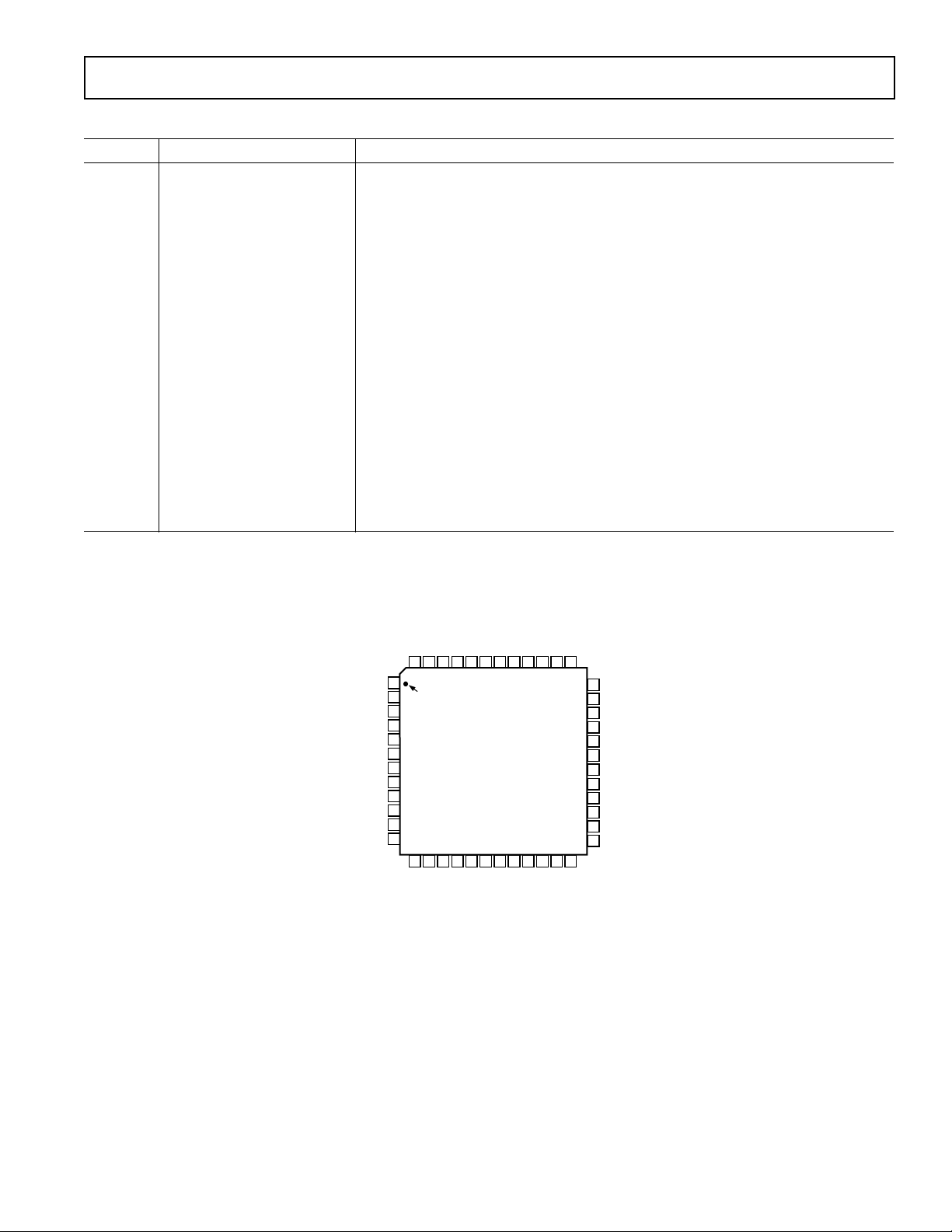
Pin No. Name Description
1–14 PORT1 Data Bits DB13–P1 to DB0–P1.
15, 21 DCOM1, DCOM2 Digital Common.
16, 22 DVDD1, DVDD2 Digital Supply Voltage.
17 WRT1/IQWRT Input write signal for PORT 1 (IQWRT in interleaving mode).
18 CLK1/IQCLK Clock input for DAC1 (IQCLK in interleaving mode).
19 CLK2/IQRESET Clock input for DAC2 (IQRESET in interleaving mode).
20 WRT2/IQSEL Input write signal for PORT 2 (IQSEL in interleaving mode).
23–36 PORT2 Data Bits DB13–P2 to DB0–P2.
37 SLEEP Power-Down Control Input.
38 ACOM Analog Common.
39, 40 I
OUTA2
, I
OUTB2
“PORT 2” differential DAC current outputs.
41 FSADJ2 Full-scale current output adjust for DAC2.
42 GAINCTRL GAINCTRL Mode (0 = 2 resistor, 1 = 1 resistor.)
43 REFIO Reference Input/Output.
44 FSADJ1 Full-scale current output adjust for DAC1.
45, 46 I
OUTB1
, I
OUTA1
“PORT 1” differential DAC current outputs.
47 AVDD Analog Supply Voltage.
48 MODE Mode Select (1 = Dual Port, 0 = Interleaved).
AD9767
DB13-P1 (MSB)
DB12-P1
DB11-P1
DB10-P1
DB9-P1
DB8-P1
DB7-P1
DB6-P1
DB5-P1
DB4-P1
DB3-P1
DB2-P1
PIN CONFIGURATION
OUTA1IOUTB1
MODE
AVDD
I
FSADJ1
REFIO
GAINCTRL
AD9767
CLK1/IQCLK
WRT1/IQWRT
FSADJ2
WRT2/IQSEL
CLK2/IQRESET
48 47 46 45 44 39 38 3743 42 41 40
1
PIN 1
2
IDENTIFIER
3
4
5
6
7
8
9
10
11
12
13 14 15 16 17 18 19 20 21 22 23 24
DB1-P1
DB0-P1
DCOM1
TOP VIEW
(Not to Scale)
DVDD1
OUTB2IOUTA2
I
DVDD2
DCOM2
ACOM
SLEEP
DB13-P2
DB12-P2
36
35
34
33
32
31
30
29
28
27
26
25
DB0-P2
DB1-P2
DB2-P2
DB3-P2
DB4-P2
DB5-P2
DB6-P2
DB7-P2
DB8-P2
DB9-P2
DB10-P2
DB11-P2
REV. B
–5–
AD9767
DEFINITIONS OF SPECIFICATIONS
Linearity Error (Also Called Integral Nonlinearity or INL)
Linearity error is defined as the maximum deviation of the
actual analog output from the ideal output, determined by a
straight line drawn from zero to full scale.
Differential Nonlinearity (or DNL)
DNL is the measure of the variation in analog value, normalized
to full scale, associated with a 1 LSB change in digital input
code.
Monotonicity
A D/A converter is monotonic if the output either increases or
remains constant as the digital input increases.
Offset Error
The deviation of the output current from the ideal of zero is
called offset error. For I
inputs are all 0s. For I
, 0 mA output is expected when the
OUTA
, 0 mA output is expected when all
OUTB
inputs are set to 1s.
Gain Error
The difference between the actual and ideal output span. The
actual span is determined by the output when all inputs are set
to 1s minus the output when all inputs are set to 0s.
Output Compliance Range
The range of allowable voltage at the output of a current-output
DAC. Operation beyond the maximum compliance limits may
cause either output stage saturation or breakdown resulting in
nonlinear performance.
Temperature Drift
Temperature drift is specified as the maximum change from the
ambient (+25°C) value to the value at either T
MIN
or T
MAX
. For
offset and gain drift, the drift is reported in ppm of full-scale
range (FSR) per degree C. For reference drift, the drift is
reported in ppm per degree C (ppm/°C).
Power Supply Rejection
The maximum change in the full-scale output as the supplies
are varied from nominal to minimum and maximum specified
voltages.
Settling Time
The time required for the output to reach and remain within a
specified error band about its final value, measured from the
start of the output transition.
Glitch Impulse
Asymmetrical switching times in a DAC give rise to undesired
output transients that are quantified by a glitch impulse. It is
specified as the net area of the glitch in pV-s.
Spurious-Free Dynamic Range
The difference, in dB, between the rms amplitude of the output
signal and the peak spurious signal over the specified bandwidth.
Total Harmonic Distortion
THD is the ratio of the rms sum of the first six harmonic
components to the rms value of the measured input signal. It is
expressed as a percentage or in decibels (dB).
R
1
SET
2k⍀
0.1F
R
SET
2k⍀
DVDD
DCOM
*RETIMED CLOCK OUTPUT
FSADJ1
REFIO
FSADJ2
2
LECROY 9210
PULSE
GENERATOR
1.2V REF
GAINCTRL
WRT1/
IQWRT
50⍀
AVDD
PMOS
CURRENT
SOURCE
ARRAY
PMOS
CURRENT
SOURCE
ARRAY
AD9767
5V
DB0 – DB13 DB0 – DB13
DIGITAL
DATA
TEKTRONIX
AWG-2021
w/OPTION 4
CLK1/IQCLK
CLK
DIVIDER
DAC 1
LATCH
DAC 2
LATCH
MULTIPLEXING LOGIC
CHANNEL 2 LATCHCHANNEL 1 LATCH
*AWG2021 CLOCK RETIMED SUCH THAT
DIGITAL DATA TRANSITIONS ON FALLING
EDGE OF 50% DUTY CYCLE CLOCK
CLK2/IQRESET
SEGMENTED
SWITCHES FOR
DAC1
SEGMENTED
SWITCHES FOR
DAC2
SWITCH
SWITCH
WRT2/
IQSEL
SLEEP
LSB
LSB
ACOM
I
OUTA1
I
OUTB1
I
OUTA2
I
OUTB2
MODE
DVDD
DCOM
50⍀ 50⍀
5V
MINI
CIRCUITS
T1-1T
TO HP3589A
SPECTRUM/
NETWORK
ANALYZER
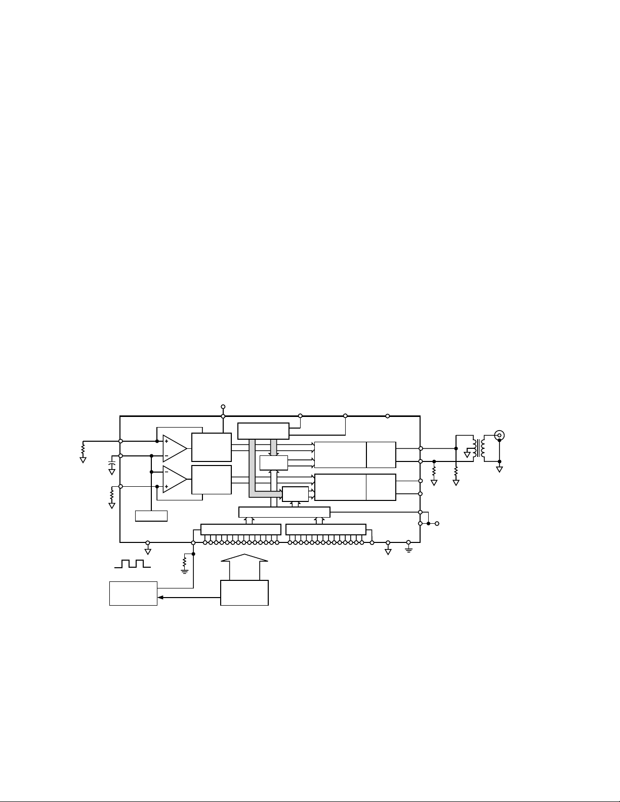
Figure 2. Basic AC Characterization Test Setup for AD9767, Testing Port 1 in Dual Port Mode, Using Independent
GAINCTRL Resistors on FSADJ1 and FSADJ2
–6–
REV. B
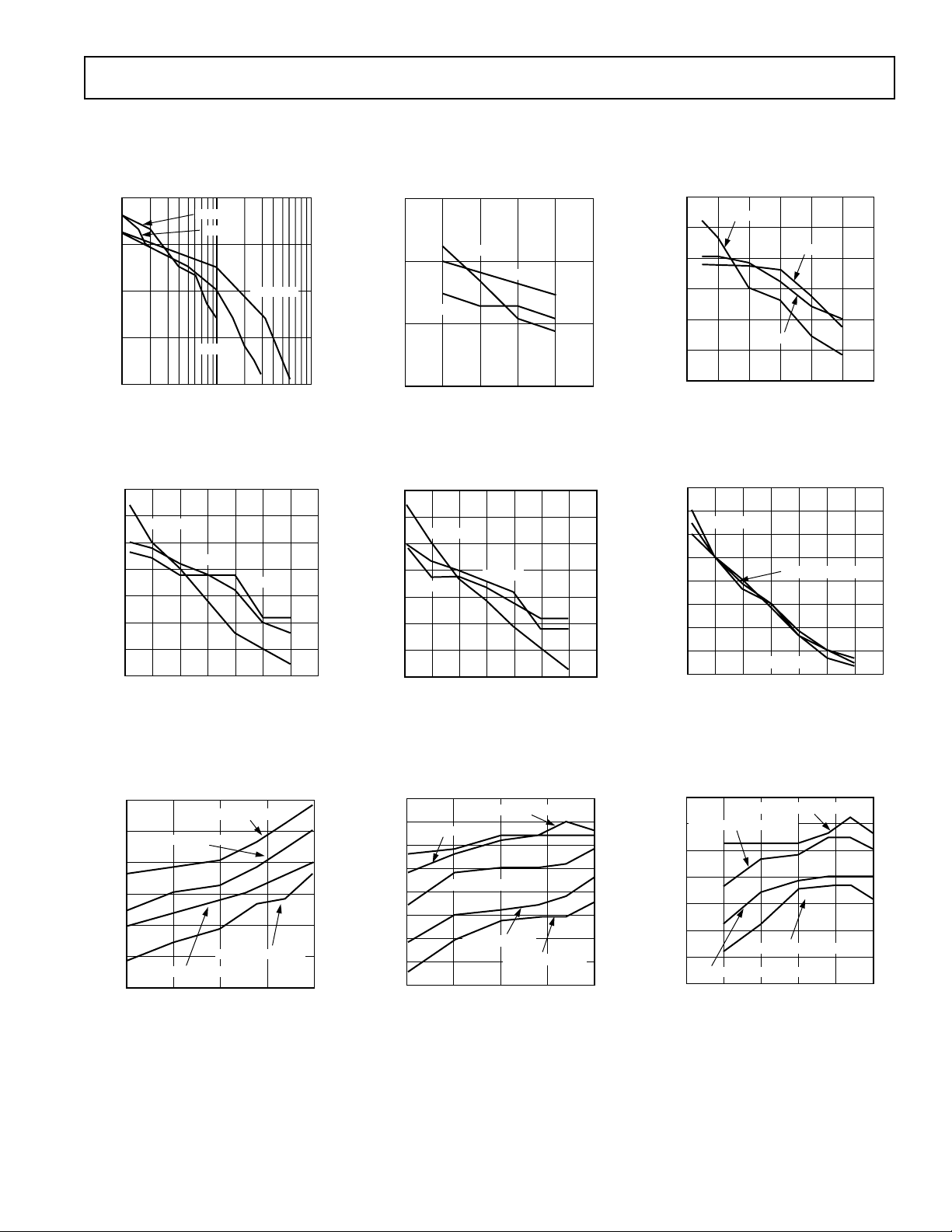
Typical Characterization Curves
(AVDD = +5 V, DVDD = +3.3 V, I
otherwise noted.)
90
5MSPS
80
70
SFDR – dBc
60
25MSPS
65MSPS
= 20 mA, 50 ⍀ Doubly Terminated Load, Differential Output, TA = +25ⴗC, SFDR up to Nyquist, unless
OUTFS
125MSPS
90
85
SFDR – dBc
80
–12dBFS
0dBFS
–6dBFS
90
85
80
75
SFDR – dBc
70
65
AD9767
0dBFS
–12dBFS
–6dBFS
50
110
Figure 3. SFDR vs. f
85
80
75
70
65
SFDR – dBc
60
55
50
05 25
Figure 6. SFDR vs. f
90
85
80
75
SFDR – dBc
70
65
60
–20 –15
f
– MHz
OUT
0dBFS
–6dBFS
10 15 20
f
OUT
910kHz/10MSPS
2.27MHz/25MSPS
5.91MHz/65MSPS
–10 –5
A
OUT
@ 0 dBFS
OUT
–12dBFS
– MHz
OUT
11.37MHz/125MSPS
– dBFS
30 35
@ 65 MSPS
Figure 9. Single-Tone SFDR vs. A
@ f
OUT
= f
CLOCK
/11
100
0
OUT
75
0.00 2.500.50 1.00 1.50 2.00
Figure 4. SFDR vs. f
85
80
75
70
–12dBFS
65
SFDR – dBc
60
55
50
010 50
Figure 7. SFDR vs. f
90
85
2MHz/10MSPS
80
75
70
SFDR – dBc
65
60
55
50
–20 –15 –5
0dBFS
20 30 40
5MHz/25MSPS
f
– MHz
OUT
OUT
–6dBFS
f
– MHz
OUT
@ 125 MSPS
OUT
1MHz/5MSPS
13MHz/65MSPS
25MHz/125MSPS
–10
A
– dBFS
OUT
@ 5 MSPS
60 70
Figure 10. Single-Tone SFDR vs.
@ f
A
OUT
OUT
= f
CLOCK
/5
60
0
Figure 5. SFDR vs. f
90
85
80
75
70
SFDR – dBc
65
60
55
50
0
Figure 8. SFDR vs. f
4
212
f
OUT
I
= 5mA
OUTFS
I
OUTFS
5152535
10
f
OUT
6
– MHz
OUT
I
= 20mA
– MHz
8
@ 25 MSPS
= 10mA
OUTFS
20 30
and I
OUT
10
OUTFS
@ 65 MSPS and 0 dBFS
85
80
75
70
65
SFDR – dBc
60
55
50
0
–25 –15 –10 –5
Figure 11. Dual-Tone SFDR vs. A
@ f
OUT
0.965/1.035MHz@7MSPS
3.38/3.63MHz@25MSPS
16.9/18.1MHz@125MSPS
6.75/7.25MHz@65MSPS
–20
A
– dBFS
OUT
= f
CLOCK
/7
0
OUT
REV. B
–7–

AD9767
75
I
= 20mA
OUTFS
70
I
= 10mA
65
SINAD – dBc
60
55
20 14040 60 80 100 120
Figure 12. SINAD vs. f
@ f
= 5 MHz and 0 dBFS
OUT
85
80
75
70
65
SFDR – dBc
60
55
50
45
–40 –20 80
–60
OUTFS
I
= 5mA
OUTFS
f
– MSPS
CLOCK
CLOCK
f
= 1MHz
OUT
f
= 10MHz
OUT
f
= 25MHz
OUT
f
= 40MHz
OUT
f
= 60MHz
OUT
TEMPERATURE – ⴗC
40200
and I
60
OUTFS
100
Figure 15. SFDR vs. Temperature @
125 MSPS, 0 dBFS
2.5
2.0
1.5
1.0
0.5
INL – LSBs
0
–0.5
–1.0
–1.5
4000 8000 12000 16000
0
CODE
Figure 13. Typical INL
0.05
GAIN ERROR
0.03
OFFSET ERROR
0.00
–0.03
OFFSET ERROR – % FS
–0.05
–40 –200 20406080
TEMPERATURE – ⴗC
1.0
0.5
0.00
–0.5
–1.0
Figure 16. Reference Voltage Drift
vs. Temperature
GAIN ERROR – % FS
0.4
0.2
0
–0.2
–0.4
–0.6
DNL – LSBs
–0.8
–1.0
–1.2
–1.4
0 200
400 600 800 1000
CODE
Figure 14. Typical DNL
10
0
–10
–20
–30
–40
dBm
–50
–60
–70
–80
–90
0
10 30
20
FREQUENCY – MHz
Figure 17. Single-Tone SFDR
@ f
= 125 MSPS
CLK
40
0
–10
–20
–30
–40
dBm
–50
–60
–70
–80
–90
0
20
10 30
FREQUENCY – MHz
Figure 18. Dual-Tone SFDR
@ f
= 125 MSPS
CLK
0
–10
–20
–30
–40
dBm
–50
–60
–70
–80
–90
0
40
10 30
20
FREQUENCY – MHz
40
Figure 19. Four-Tone SFDR
= 125 MSPS
@ f
CLK
–8–
REV. B
AD9767
+1.2V
REF
AVDD
GAINCTRL
CURRENT
SOURCE
ARRAY
REFIO
FSADJ
2k⍀
AD9767
REFERENCE
SECTION
I
REF
ACOM
AVDD
EXTERNAL
REFERENCE
I
REF
5V
CURRENT
CURRENT
AD9767
WRT1/
IQWRT
AVDD
PMOS
SOURCE
ARRAY
PMOS
SOURCE
ARRAY
MULTIPLEXING LOGIC
DB0 – DB13 DB0 – DB13
R
1
SET
2k⍀
1
I
2
REF
0.1F
R
SET
2k⍀
FSADJ1
REFIO
2
FSADJ2
1.2V REF
GAINCTRL
CLK1/IQCLK
CLK
DIVIDER
DAC 1
LATCH
DAC 2
LATCH
DIGITAL DATA INPUTS
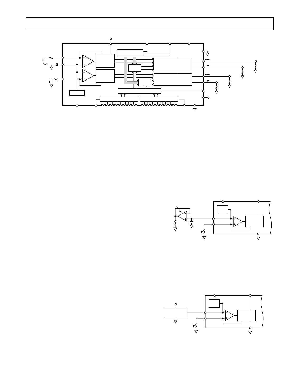
Figure 20. Simplified Block Diagram
FUNCTIONAL DESCRIPTION
Figure 20 shows a simplified block diagram of the AD9767.
The AD9767 consists of two DACs, each with its own independent digital control logic and full-scale output current control.
Each DAC contains a PMOS current source array capable of
providing up to 20 mA of full-scale current (I
OUTFS
). The array
is divided into 31 equal currents that make up the five most
significant bits (MSBs). The next four bits, or middle bits,
consist of 15 equal current sources whose value is 1/16th of an
MSB current source. The remaining LSB is a binary weighted
fraction of the middle bit current sources. Implementing the
middle and lower bits with current sources, instead of an R-2R
ladder, enhances the dynamic performance for multitone or low
amplitude signals and helps maintain the DAC’s high output
impedance (i.e., >100 kΩ).
All of these current sources are switched to one or the other of
the two output nodes (i.e., I
OUTA
or I
) via PMOS differen-
OUTB
tial current switches. The switches are based on a new architecture that drastically improves distortion performance. This new
switch architecture reduces various timing errors and provides
matching complementary drive signals to the inputs of the differential current switches.
The analog and digital sections of the AD9767 have separate
power supply inputs (i.e., AVDD and DVDD) that can operate
independently over a 3 V to 5.5 V range. The digital section,
which is capable of operating up to a 125 MSPS clock rate,
consists of edge-triggered latches and segment decoding logic
circuitry. The analog section includes the PMOS current sources,
the associated differential switches, a 1.20 V bandgap voltage
reference and two reference control amplifiers.
The full-scale output current of each DAC is regulated by separate reference control amplifiers and can be set from 2 mA to
20 mA via an external resistor, R
, connected to the Full
SET
Scale Adjust (FSADJ) pin. The external resistor, in combination
with both the reference control amplifier and voltage reference
, sets the reference current I
V
REFIO
, which is replicated to the
REF
segmented current sources with the proper scaling factor. The
full-scale current, I
REV. B
, is 32 × I
OUTFS
REF
.
–9–
CLK2/IQRESET
SWITCHES FOR
SEGMENTED
SWITCHES FOR
CHANNEL 2 LATCHCHANNEL 1 LATCH
SEGMENTED
DAC1
DAC2
SLEEP
LSB
SWITCH
LSB
SWITCH
WRT2/
IQSEL
ACOM
I
OUTA1
I
OUTB1
I
OUTA2
I
OUTB2
MODE
DVDD
DCOM
= V
A – V
V
DIFF
OUT
2A
V
OUT
V
2B
RL2B
50⍀
RL2A
50⍀
OUT
5V
B
OUT
1A
V
OUT
V
1B
RL1B
50⍀
RL1A
50⍀
OUT
REFERENCE OPERATION
The AD9767 contains an internal 1.20 V bandgap reference.
This can easily be overridden by an external reference with no
effect on performance. REFIO serves as either an input or out-
put, depending on whether the internal or an external reference
is used. To use the internal reference, simply decouple the
REFIO pin to ACOM with a 0.1 µF capacitor. The internal
reference voltage will be present at REFIO. If the voltage at
REFIO is to be used elsewhere in the circuit, an external buffer
amplifier with an input bias current of less than 100 nA should
be used. An example of the use of the internal reference is
shown in Figure 21.
OPTIONAL
EXTERNAL
REFERENCE
BUFFER
ADDITIONAL
EXTERNAL
LOAD
0.1F
I
REF
2k⍀
GAINCTRL
+1.2V
REF
REFIO
FSADJ
AD9767
REFERENCE
SECTION
AVDD
CURRENT
SOURCE
ARRAY
ACOM
Figure 21. Internal Reference Configuration
An external reference can be applied to REFIO as shown in
Figure 22. The external reference may provide either a fixed
reference voltage to enhance accuracy and drift performance or
a varying reference voltage for gain control. Note that the 0.1 µF
compensation capacitor is not required since the internal reference is overridden, and the relatively high input impedance of
REFIO minimizes any loading of the external reference.
Figure 22. External Reference Configuration
 Loading...