®
ACOM
REFLO
I
DAC
FSADJ
IOUTA
IOUTB
WRITE INPUT
SELECT INPUT
DCOM
DVDD
CLOC
K
AD9761
2
LATCH
I
REFIO
REFERENCE
COMP1
COMP2
COMP3
BIAS
GENERATOR
QOUTA
QOUTB
2
LATCH
Q
MUX
CONTROL
AVDD
DAC DAT
A
INPUT
S
(10 BITS)
SLEEP
Q
DAC
Dual 10-Bit TxDAC+
with 2 Interpolation Filters
AD9761
FEATURES
Complete 10-Bit, 40 MSPS Dual Transmit DAC
Excellent Gain and Offset Matching
Differential Nonlinearity Error: 0.5 LSB
Effective Number of Bits: 9.5
Signal-to-Noise and Distortion Ratio: 59 dB
Spurious-Free Dynamic Range: 71 dB
2 Interpolation Filters
20 MSPS/Channel Data Rate
Single Supply: 3 V to 5.5 V
Low Power Dissipation: 93 mW (3 V Supply @
40 MSPS)
On-Chip Reference
28-Lead SSOP
PRODUCT DESCRIPTION
The AD9761 is a complete dual-channel, high speed, 10-bit
CMOS DAC. The AD9761 has been developed specically for
use in wide bandwidth communication applications (e.g., spread
spectrum) where digital I and Q information is being processed
during transmit operations. It integrates two 10-bit, 40 MSPS
DACs, dual 2 interpolation lters, a voltage reference, and digital input interface circuitry. The AD9761 supports a 20 MSPS
per channel input data rate that is then interpolated by 2 up to
40 MSPS before simultaneously updating each DAC.
The interleaved I and Q input data stream is presented to the
digital interface circuitry, which consists of I and Q latches as
well as some additional control logic. The data is de-interleaved
back into its original I and Q data. An on-chip state machine
ensures the proper pairing of I and Q data. The data output from
each latch is then processed by a 2 digital interpolation lter
that eases the reconstruction lter requirements. The interpolated output of each lter serves as the input of their respective
10-bit DAC.
The DACs utilize a segmented current source architecture combined with a proprietary switching technique to reduce glitch
energy and to maximize dynamic accuracy. Each DAC provides
differential current output, thus supporting single-ended or differential applications. Both DACs are simultaneously updated
and provide a nominal full-scale current of 10 mA. Also, the
full-scale currents between each DAC are matched to within
0.07 dB (i.e., 0.75%), thus eliminating the need for additional
gain calibration circuitry.
The AD9761 is manufactured on an advanced low cost CMOS
process. It operates from a single supply of 3 V to 5.5 V and
consumes 200 mW of power. To make the AD9761 complete, it
also offers an internal 1.20 V temperature-compensated band gap
reference.
REV. C
Information furnished by Analog Devices is believed to be accurate and
reliable. However, no responsibility is assumed by Analog Devices for its
use, nor for any infringements of patents or other rights of third parties
that may result from its use. No license is granted by implication or otherwise under any patent or patent rights of Analog Devices. Trademarks
and registered trademarks are the property of their respective companies.
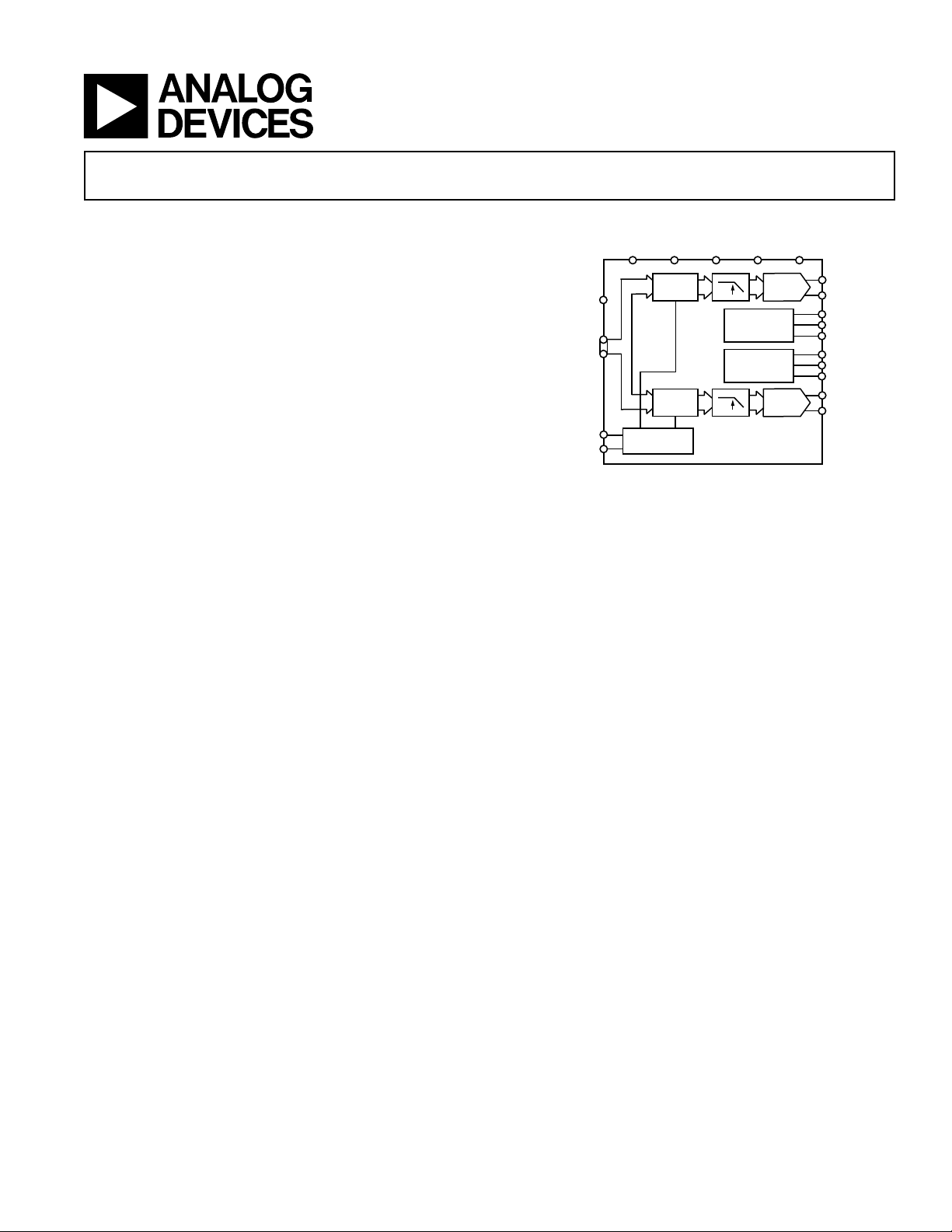
FUNCTIONAL BLOCK DIAGRAM
PRODUCT HIGHLIGHTS
1. Dual 10-Bit, 40 MSPS DACs
A pair of high performance 40 MSPS DACs optimized for low
distortion performance provide for exible transmission of I
and Q information.
2. 2 Digital Interpolation Filters
Dual matching FIR interpolation lters with 62.5 dB stop-
band rejection precede each DAC input, thus reducing the
DACs’ reconstruction lter requirements.
3. Low Power
Complete CMOS dual DAC function operates on a low
200 mW on a single supply from 3 V to 5.5 V. The DAC
full-scale current can be reduced for lower power operation, and a sleep mode is provided for power reduction
during idle periods.
4. On-Chip Voltage Reference
The AD9761 includes a 1.20 V temperature-compensated
band gap voltage reference.
5. Single 10-Bit Digital Input Bus
The AD9761 features a exible digital interface that allows
each DAC to be addressed in a variety of ways including different update rates.
6. Small Package
The AD9761 offers the complete integrated function in a
compact 28-lead SSOP package.
7. Product Family
The AD9761 Dual Transmit DAC has a pair of Dual Receive
ADC companion products, the AD9281 (8 bits) and AD9201
(10 bits).
One Technology Way, P.O. Box 9106, Norwood, MA 02062-9106, U.S.A.
Tel: 781/329-4700 www.analog.com
Fax: 781/326-8703 © 2003 Analog Devices, Inc. All rights reserved.

AD9761–SPECIFICATIONS
(T
to T
DC SPECIFICATIONS
MIN
, AVDD = 5 V, DVDD = 5 V, I
Max
Parameter Min Typ Max Unit
RESOLUTION 10 Bits
DC ACCURACY
1
Integral Nonlinearity Error (INL)
TA = 25°C –1.75 ±0.5 +1.75 LSB
T
to T
MIN
MAX
Differential Nonlinearity (DNL)
–2.75 ±0.7 +2.75 LSB
TA = 25°C –1 ±0.4 +1.25 LSB
T
MIN
to T
MAX
–1 ±0.5 +1.75 LSB
Monotonicity (10-Bit) Guaranteed over Rated Specication Temperature Range
ANALOG OUTPUT
Offset Error –0.05 ±0.025 +0.05 % of FSR
Offset Matching between DACs –0.10 ±0.05 +0.10 % of FSR
Gain Error (without Internal Reference) –5.5 ±1.0 +5.5 % of FSR
Gain Error (with Internal Reference) –5.5 ±1.0 +5.5 % of FSR
Gain Matching between DACs –1.0 ±0.25 +1.0 % of FSR
Full-Scale Output Current2 10 mA
Output Compliance Range –1.0 +1.25 V
Output Resistance 100 k
Output Capacitance 5 pF
REFERENCE OUTPUT
Reference Voltage 1.14 1.20 1.26 V
Reference Output Current
3
REFERENCE INPUT
Input Compliance Range 0.1 1.25 V
Reference Input Resistance 1 M
TEMPERATURE COEFFICIENTS
Unipolar Offset Drift 0 ppm/°C
Gain Drift (without Internal Reference) ±50 ppm/°C
Gain Drift (with Internal Reference) ±140 ppm/°C
Gain Matching Drift (between DACs) ±25 ppm/°C
Reference Voltage Drift ±50 ppm/°C
POWER SUPPLY
AVDD
Voltage Range 3.0 5.0 5.5 V
Analog Supply Current (I
) 26 29 mA
AVDD
DVDD
Voltage Range 2.7 5.0 5.5 V
Digital Supply Current at 5 V (I
Digital Supply Current at 3 V (I
Nominal Power Dissipation
5
)4 15 18 mA
DVDD
)4 5 mA
DVDD
AVDD and DVDD at 3 V 93 mW
AVDD and DVDD at 5 V 200 250 mW
Power Supply Rejection Ratio (PSRR)–AVDD –0.25 +0.25 % of FSR/V
Power Supply Rejection Ratio (PSRR)–DVDD –0.02 +0.02 % of FSR/V
OPERATING RANGE –40 +85 °C
NOTES
1
Measured at IOUTA and QOUTA, driving a virtual ground.
2
Nominal full-scale current, I
3
Use an external amplier to drive any external load.
4
Measured at f
5
Measured as unbuffered voltage output into 50 R
Specications subject to change without notice.
= 40 MSPS and f
CLOCK
, is 16 the I
OUTFS
= 1 MHz.
OUT
current.
REF
at IOUTA, IOUTB, QOUTA, and QOUTB; f
LOAD
= 10 mA, unless otherwise noted.)
OUTFS
100 nA
= 40 MSPS and f
CLOCK
= 8 MHz.
OUT
–2–
REV. C
AD9761
I DATA Q DATA
t
CINV
DB9–DB0
DAC
INPUTS
SELECT
WRITE
CLOCK
t
S
t
H
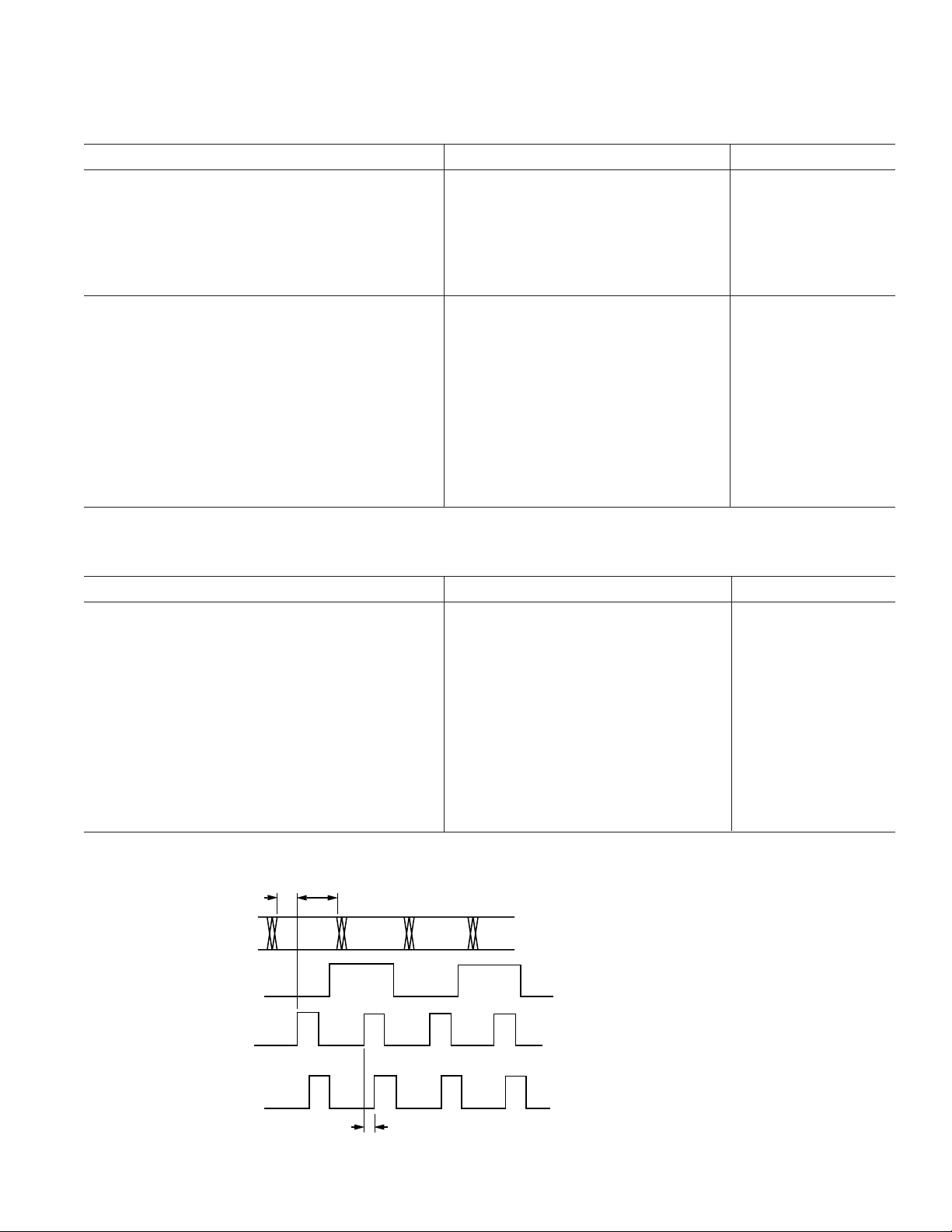
NOTE: WRITE AND CLOCK CAN BE
TIED TOGETHER. FOR TYPICAL EXAMPLES,
REFER TO DIGITAL INPUTS AND INTERLEAVED
INTERFACE CONSIDERATION SECTION.
(T
to T
, AVDD = 5 V, DVDD = 5 V, I
MAX
DYNAMIC SPECIFICATIONS
MIN
50 Doubly Terminated, unless otherwise noted.)
Parameter Min Typ Max Unit
DYNAMIC PERFORMANCE
Maximum Output Update Rate 40 MSPS
Output Settling Time (tST to 0.025%) 35 ns
Output Propagation Delay (tPD) 55 Input Clock Cycles
Glitch Impulse 5 pV-s
Output Rise Time (10% to 90%) 2.5 ns
Output Fall Time (10% to 90%) 2.5 ns
AC LINEARITY TO NYQUIST
Signal-to-Noise and Distortion (SINAD)
f
= 1 MHz; CLOCK = 40 MSPS 56 59 dB
OUT
Effective Number of Bits (ENOBs) 9.0 9.5 Bits
Total Harmonic Distortion (THD)
f
= 1 MHz; CLOCK = 40 MSPS
OUT
TA = 25°C –68 –58 dB
T
MIN
to T
–67 –53 dB
MAX
Spurious-Free Dynamic Range (SFDR)
f
= 1 MHz; CLOCK = 40 MSPS; 10 MHz Span 59 68 dB
OUT
Channel Isolation
f
Specications subject to change without notice.
= 8 MHz; CLOCK = 40 MSPS; 10 MHz Span 90 dBc
OUT
= 10 mA, Differential Transformer Coupled Output,
OUTFS
DIGITAL SPECIFICATIONS
MIN
, AVDD = 5 V, DVDD = 5 V, I
MAX
= 10 mA unless otherwise noted.)
OUTFS
(T
to T
Parameter Min Typ Max Unit
DIGITAL INPUTS
Logic 1 Voltage @ DVDD = 5 V 3.5 5 V
Logic 1 Voltage @ DVDD = 3 V 2.4 3 V
Logic 0 Voltage @ DVDD = 5 V 0 1.3 V
Logic 0 Voltage @ DVDD = 3 V 0 0.9 V
Logic 1 Current –10 +10 µA
Logic 0 Current –10 +10 µA
Input Capacitance 5 pF
Input Setup Time (tS) 3 ns
Input Hold Time (tH) 2 ns
CLOCK High 5 ns
CLOCK Low 5 ns
Invalid CLOCK/WRITE Window (t
*t
is an invalid window of 4 ns duration beginning 1 ns after the rising edge of WRITE in which the rising edge of CLOCK must not occur.
CINV
Specications subject to change without notice.
CINV
)*
1 5 ns
REV. C
Figure 1. Timing Diagram
–3–
AD9761
AD9761
–5–
FREQUENCY RESPONSE (DC to f
CLOCK
/2)
OUTPUT (dBFS)
0
–20
–120
0 0.50.1 0.2 0.3 0.4
–40
–60
–80
–100
TIME (Samples)
1
0
0 405 10 15 20 25 30 35
0.9
0.6
0.4
0.2
0.1
0.8
0.7
0.5
0.3
–0.1
–0.2
–0.3
NORMALIZED OUTPUT
REV. C
DIGITAL FILTER SPECIFICATIONS
(T
to T
MIN
, AVDD = 2.7 V to 5.5 V, DVDD = 2.7 V to 5.5 V, I
MAX
otherwise noted.)
= 10 mA, unless
OUTFS
Parameter Min Typ Max Unit
MAXIMUM INPUT CLOCK RATE (f
) 40 MSPS
CLOCK
DIGITAL FILTER CHARACTERISTICS
Pass Bandwidth1: 0.005 dB 0.2010 f
Pass Bandwidth: 0.01 dB 0.2025 f
Pass Bandwidth: 0.1 dB 0.2105 f
Pass Bandwidth: –3 dB 0.239 f
OUT/fCLOCK
OUT/fCLOCK
OUT/fCLOCK
OUT/fCLOCK
Linear Phase (FIR Implementation)
Stop-Band Rejection: 0.3 f
Group Delay
2
Impulse Response Duration
CLOCK
3
to 0.7 f
–62.5 dB
CLOCK
32 Input Clock Cycles
–40 dB 28 Input Clock Cycles
–60 dB 40 Input Clock Cycles
NOTES
1
Excludes SINx/x characteristic of DAC.
2
Dened as the number of data clock cycles between impulse input and peak of output response.
3
55 input clock periods from input to I DAC, 56 to Q DAC. Propagation delay is delay from data input to DAC update.
Specications subject to change without notice.
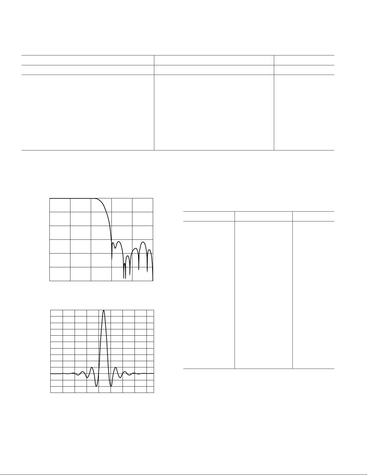
Table I. Integer Filter Coefcients for 43-Tap Half-Band
FIR Filter
Lower Coefcient Upper Coefcient Integer Value
H(1) H(43) 1
H(2) H(42) 0
H(3) H(41) –3
H(4) H(40) 0
H(5) H(39) 8
H(6) H(38) 0
H(7) H(37) –16
H(8) H(36) 0
H(9) H(35) 29
H(10) H(34) 0
H(11) H(33) –50
Figure 2a. FIR Filter Frequency Response
H(12) H(32) 0
H(13) H(31) 81
H(14) H(30) 0
H(15) H(29) –131
H(16) H(28) 0
H(17) H(27) 216
H(18) H(26) 0
H(19) H(25) –400
H(20) H(24) 0
H(21) H(23) 1264
H(22) 1998
Figure 2b. FIR Filter Impulse Response
–4–
REV. C
AD9761
COMP1
I
DAC
FSADJ
IOUTA
IOUTB
WRITE
SELECT
COMP2 AVDD AVSS
AD9761
2x
LATCH
I
REFLO
Q
DAC
QOUTA
QOUTB2x
LATCH
Q
MUX
CONTROL
COMP3
DB9–DB0
SLEEPCLOCK
REFIO
100
50
20pF
50
20pF
DIGITAL
DATA
TEKTRONIX
AWG-2021
CLOCK
OUT
MARKER 1
RETIMED
CLOCK
OUTPUT*
LE CROY 9210
PULSE GENERATOR
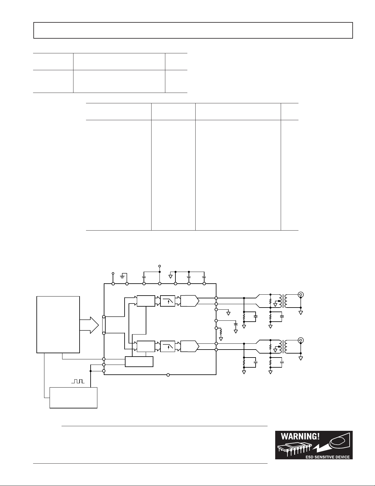
*AWG2021 CLOCK RETIMED SUCH THAT DIGITAL DATA
TRANSITIONS ON FALLING EDGE OF 50% DUTY CYCLE CLOCK.
MINI-CIRCUITS
T1-1T
R
SET
2k
0.1F
TO HP3589A
SPECTRUM/NETWOR
K
ANALYZER
50 INPUT
100
50
20pF
50
20pF
MINI-CIRCUITS
T1-1T
TO HP3589A
SPECTRUM/NETWOR
K
ANALYZER
50 INPUT
0.1F 0.1F0.1F
DVDD DCOM
2.7V TO
5.5V
3V TO
5.5V
ORDERING GUIDE
Package Package
Model Description Option
AD9761ARS 28-Lead Shrink Small Outline (SSOP) RS-28
AD9761ARSRL 28-Lead Shrink Small Outline (SSOP) RS-28
AD9761-EB Evaluation Board
ABSOLUTE MAXIMUM RATINGS*
With
Parameter Respect to Min Max Unit
AVDD ACOM –0.3 +6.5 V
DVDD DCOM –0.3 +6.5 V
ACOM DCOM –0.3 +0.3 V
AVDD DVDD –6.5 +6.5 V
CLOCK, WRITE DCOM –0.3 DVDD + 0.3 V
SELECT, SLEEP DCOM –0.3 DVDD + 0.3 V
Digital Inputs DCOM –0.3 DVDD + 0.3 V
IOUTA, IOUTB ACOM –1.0 AVDD + 0.3 V
QOUTA, QOUTB ACOM –1.0 AVDD + 0.3 V
COMP1, COMP2 ACOM –0.3 AVDD + 0.3 V
COMP3 ACOM –0.3 AVDD + 0.3 V
REFIO, FSADJ ACOM –0.3 AVDD + 0.3 V
REFLO ACOM –0.3 +0.3 V
Junction Temperature 150 °C
Storage Temperature –65 +150 °C
Lead Temperature (10 sec) 300 °C
*Stresses above those listed under Absolute Maximum Ratings may cause permanent damage to the device. This
is a stress rating only; functional operation of the device at these or any other conditions above those indicated in
the operational sections of this specication is not implied. Exposure to absolute maximum ratings for extended
periods may affect device reliability.
THERMAL CHARACTERISTICS
Thermal Resistance
28-Lead SSOP
q
= 109°C/W
JA
Figure 3. Basic AC Characterization Test Setup
CAUTION
ESD (electrostatic discharge) sensitive device. Electrostatic charges as high as 4000 V readily accumulate on
the human body and test equipment and can discharge without detection. Although the AD9761 features
proprietary ESD protection circuitry, permanent damage may occur on devices subjected to high energy
electrostatic discharges. Therefore, proper ESD precautions are recommended to avoid performance
degradation or loss of functionality.
REV. C
–5–
AD9761
AD9761
–7–
14
13
12
11
17
16
15
20
19
18
10
9
8
1
2
3
4
7
6
5
TOP VIEW
(Not to Scale)
28
27
26
25
24
23
22
21
AD9761
(MSB) DB9
IOUTB
IOUTA
COMP1
RESET/SLEEP
DB8
DB7
DB6
COMP2
AVDD
ACOM
DB5
DB4
DB3
DB2
DB1
(LSB) DB0 REFLO
REFIO
FSADJ
CLOCK
WRITE
SELECT
DVDD
QOUTB
DCOM
COMP3
QOUTA
REV. C
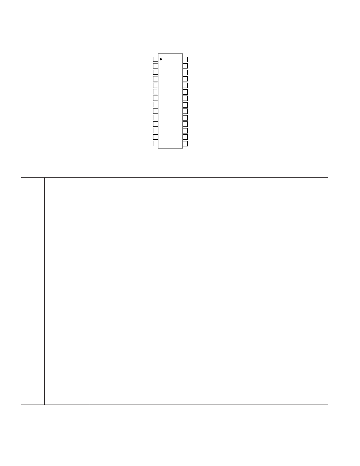
Pin No. Mnemonic Description
1 DB9 Most Signicant Data Bit (MSB).
2–9 DB8–DB1 Data Bits 1–8.
10 DB0 Least Signicant Data Bit (LSB).
11 CLOCK Clock Input. Both DACs’ outputs updated on positive edge of clock and digital lters read respective
input registers.
12 WRITE Write Input. DAC input registers latched on positive edge of write.
13 SELECT Select Input. Select high routes input data to I DAC; select low routes data to Q DAC.
14 DVDD Digital Supply Voltage (2.7 V to 5.5 V).
15 DCOM Digital Common.
16 COMP3 Internal Bias Node for Switch Driver Circuitry. Decouple to ACOM with 0.1 µF capacitor.
17 QOUTA Q DAC Current Output. Full-scale current when all data bits are 1s.
18 QOUTB Q DAC Complementary Current Output. Full-scale current when all data bits are 0s.
19 REFLO Reference Ground when Internal 1.2 V Reference Used. Connect to AVDD to disable internal reference.
20 REFIO Reference Input/Output. Serves as reference input when internal reference disabled. Serves as 1.2 V
reference output when internal reference activated. Requires 0.1 µF capacitor to ACOM when internal
reference activated.
21 FSADJ Full-Scale Current Output Adjust. Resistance to ACOM sets full-scale output current.
22 COMP2 Bandwidth/Noise Reduction Node. Add 0.1 µF to AVDD for optimum performance.
23 AVDD Analog Supply Voltage (3 V to 5.5 V).
24 ACOM Analog Common.
25 IOUTB I DAC Complementary Current Output. Full-scale current when all data bits are 0s.
26 IOUTA I DAC Current Output. Full-scale current when all data bits are 1s.
27 COMP1 Internal Bias Node for Switch Driver Circuitry. Decouple to AGND with 0.1 µF capacitor.
28 RESET/SLEEP Power-Down Control Input if Asserted for Four Clock Cycles or Longer. Reset control input if
asserted for less than four clock cycles. Active high. Connect to DCOM if not used. Refer to RESET/
SLEEP Mode Operation section.
PIN CONFIGURATION
PIN FUNCTION DESCRIPTIONS
–6–
REV. C

AD9761
DEFINITIONS OF SPECIFICATIONS
Linearity Error
(Also Called Integral Nonlinearity or INL)
Linearity error is dened as the maximum deviation of the
actual analog output from the ideal output, determined by a
straight line drawn from zero to full scale.
Differential Nonlinearity (DNL)
DNL is the measure of the variation in analog value, normalized
to full scale, associated with a 1 LSB change in digital input code.
Monotonicity
A D/A converter is monotonic if the output either increases or
remains constant as the digital input increases.
Offset Error
The deviation of the output current from the ideal of zero is
called offset error. For IOUTA, 0 mA output is expected when
the inputs are all 0s. For IOUTB, 0 mA output is expected when
all inputs are set to 1s.
Gain Error
The difference between the actual and ideal output span. The
actual span is determined by the output when all inputs are set to
1s minus the output when all inputs are set to 0s.
Output Compliance Range
The range of allowable voltage at the output of a current-output
DAC. Operation beyond the maximum compliance limits may
cause either output stage saturation or breakdown, resulting in
nonlinear performance.
Temperature Drift
Temperature drift is specied as the maximum change from the
ambient (25°C) value to the value at either T
MIN
or T
MAX
. For
offset and gain drift, the drift is reported in ppm of full-scale
range (FSR) per °C. For reference drift, the drift is reported in
ppm per °C.
Power Supply Rejection
The maximum change in the full-scale output as the supplies
are varied from nominal to minimum and maximum specied
voltages.
Settling Time
The time required for the output to reach and remain within a
specied error band about its nal value, measured from the start
of the output transition.
Glitch Impulse
Asymmetrical switching times in a DAC give rise to undesired
output transients that are quantied by a glitch impulse. It is
specied as the net area of the glitch in pV-s.
Channel Isolation
Channel Isolation is a measure of the level of crosstalk between
channels. It is measured by producing a full-scale 8 MHz signal
output for one channel and measuring the leakage into the other
channel.
Spurious-Free Dynamic Range
The difference, in dB, between the rms amplitude of the output
signal and the peak spurious signal over the specied bandwidth.
Total Harmonic Distortion
THD is the ratio of the sum of the rms value of the rst six
harmonic components to the rms value of the measured output
signal. It is expressed as a percentage or in decibels (dB).
Signal-to-Noise and Distortion (S/N+D, SINAD) Ratio
S/N+D is the ratio of the rms value of the measured output
signal to the rms sum of all other spectral components below the
Nyquist frequency, including harmonics but excluding dc. The
value for S/N+D is expressed in decibels.
Effective Number of Bits (ENOB)
For a sine wave, SINAD can be expressed in terms of the number
of bits. Using the following formula,
N = (SINAD – 1.76)/6.02
it is possible to get a measure of performance expressed as N, the
effective number of bits.
Thus, effective number of bits for a device for sine wave inputs
at a given input frequency can be calculated directly from its
measured SINAD.
Pass Band
Frequ enc y band in wh ich a ny inpu t app lied there in
passe s unattenuated to the DAC output.
Stop-Band Rejection
The amount of attenuation of a frequency outside the pass band
applied to the DAC, relative to a full-scale signal applied at the
DAC input within the pass band.
Group Delay
Numbe r of input c loc ks be tw ee n a n impul se ap plied at
the device input and peak DAC output current.
Impulse Response
Response of the device to an impulse applied to the input.
REV. C
–7–
AD9761—Typical Performance Characteristics
AD9761
–9–
0
–10
–20
–30
–40
–50
–70
–60
–80
–90
START: 0Hz
STOP: 40MHz
10dB (Div)
–100
f
(MHz)
dB
75
70
60
65
2.0 4.0 10.0
S/E 0dBFS
DIFF 0dBFS
S/E –6dBFS
DIFF –6dBFS
55
50
0 6.0 8.0
f
OUT
(MHz)
dB
80
70
SFDR @ 10mA
65
2
75
60
55
0
SINAD @ 10mA
SFDR @ 5mA
SINAD @ 5mA
SFDR @ 2.5mA
SINAD @ 2.5mA
4 6 8 10
f
OUT
(MHz)
dB
65
60
50
55
0 2.0 10.04.0 6.0 8.0
10.50
9.67
8.01
8.84
ENOB
S/E 0dBFS
DIFF 0dBFS
S/E –6dBFS
DIFF –6dBFS
A
(dBFS)
dB
80
75
60
65
–25 –20 –5
SFDR @ 40MSPS
55
50
–30 –15 –10
SINAD @ 40MSPS
SFDR @ 20MSPS
SINAD @ 20MSPS
SFDR @ 10MSPS
SINAD @ 10MSPS
70
45
40
35
–0
f
OUT
(MHz)
dB
80
70
SFDR @ 10mA
65
2
75
60
55
0
SINAD @ 10mA
SFDR @ 5mA
SINAD @ 5mA
SFDR @ 2.5mA
SINAD @ 2.5mA
4 6 8 10
f
OUT
(MHz)
dB
80
75
65
70
0 5.0 10.0
S/E 0dBFS
DIFF 0dBFS
S/E –6dBFS
DIFF –6dBFS
A
(dBFS)
dB
80
75
60
65
–25 –20 –5
SFDR @ 40MSPS
55
50
–30 –15 –10
SINAD @ 40MSPS
SFDR @ 20MSPS
SINAD @ 20MSPS
SFDR @ 10MSPS
SINAD @ 10MSPS
70
45
40
35
0
–45
–65
–55
–75
–85
START: 0Hz
STOP: 20MHz
10dB (Div)
–105
–95
REV. C
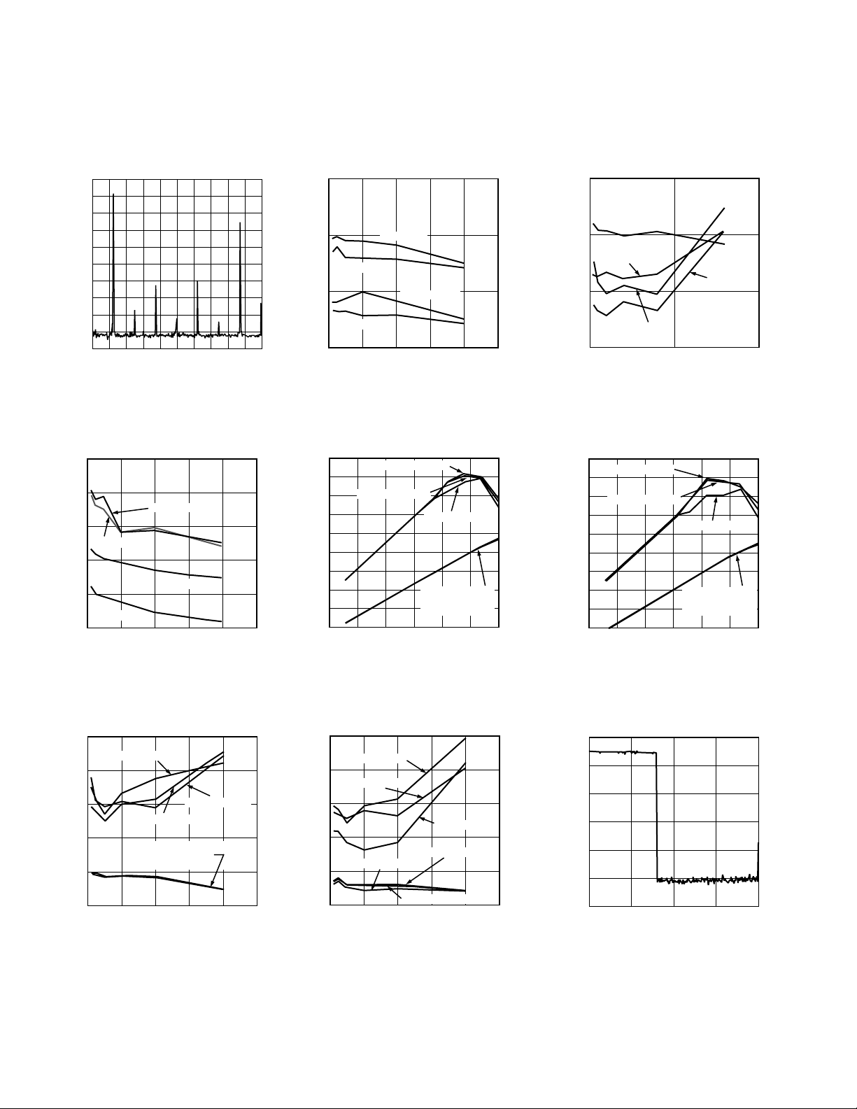
Typical AC Characterization Curves @ 5 V Supplies
(AVDD = 5 V, DVDD = 5 V, 50 Doubly Terminated Load, TA = 25C, f
performance shown.)
= 40 MSPS, unless otherwise noted, worst of I or Q output
CLOCK
TPC 1. Single-Tone SFDR (DC
to 2 f
DATA
, f
CLOCK
= 2 f
DATA
TPC 4. Out-of-Band SFDR vs.
f
(f
OUT
/2 to 3/2 f
DATA
DATA
TPC 2. SINAD (ENOBs) vs.
f
)
OUT
(DC to f
TPC 5. SINAD vs. A
f
)
/2, Differential Output)
DATA
DATA
/2)
OUT
(DC to
TPC 3. SFDR vs. f
TPC 6. SINAD vs. A
f
/2, Single-Ended Output)
DATA
(DC to f
OUT
OUT
(DC to
DATA
/2)
TPC 7. SINAD/SFDR vs. I
(DC to f
/2, Differential Output)
DATA
OUTFS
TPC 8. SINAD/SFDR vs. I
(DC to f
/2, Single-Ended Output)
DATA
–8–
OUTFS
TPC 9. Wideband SpreadSpectrum Spectral Plot (DC to f
DATA
)
REV. C
 Loading...