a
10-Bit, 300 MSPS
High Speed TxDAC+
®
D/A Converter
FEATURES
10-Bit Dual Muxed Port DAC
300 MSPS Output Update Rate
Excellent SFDR and IMD Performance
SFDR to Nyquist @ 25 MHz Output: 64 dB
Internal Clock Doubling PLL
Differential or Single-Ended Clock Input
On-Chip 1.2 V Reference
Single 3.3 V Supply Operation
Power Dissipation: 155 mW @ 3.3 V
48-Lead LQFP
APPLICATIONS
Communications: LMDS, LMCS, MMDS
Base Stations
Digital Synthesis
QAM and OFDM
PRODUCT DESCRIPTION
The AD9751 is a dual muxed port, ultrahigh speed, singlechannel, 10-bit CMOS DAC. It integrates a high quality 10-bit
TxDAC+
core, a voltage reference, and digital interface circuitry
into a small 48-lead LQFP package. The AD9751 offers exceptional ac and dc performance while supporting update rates up
to 300 MSPS.
The AD9751 has been optimized for ultrahigh speed applications up to 300 MSPS where data rates exceed those possible on
a single data interface port DAC. The digital interface consists
of two buffered latches as well as control logic. These latches
can be time multiplexed to the high speed DAC in several ways.
This PLL drives the DAC latch at twice the speed of the externally applied clock and is able to interleave the data from the
two input channels. The resulting output data rate is twice that
of the two input channels. With the PLL disabled, an external
2× clock may be supplied and divided by two internally.
The CLK inputs (CLK+/CLK–) can be driven either differentially or single-ended, with a signal swing as low as 1 V p-p.
I
OUTA
I
OUTB
REFIO
FSADJ
*
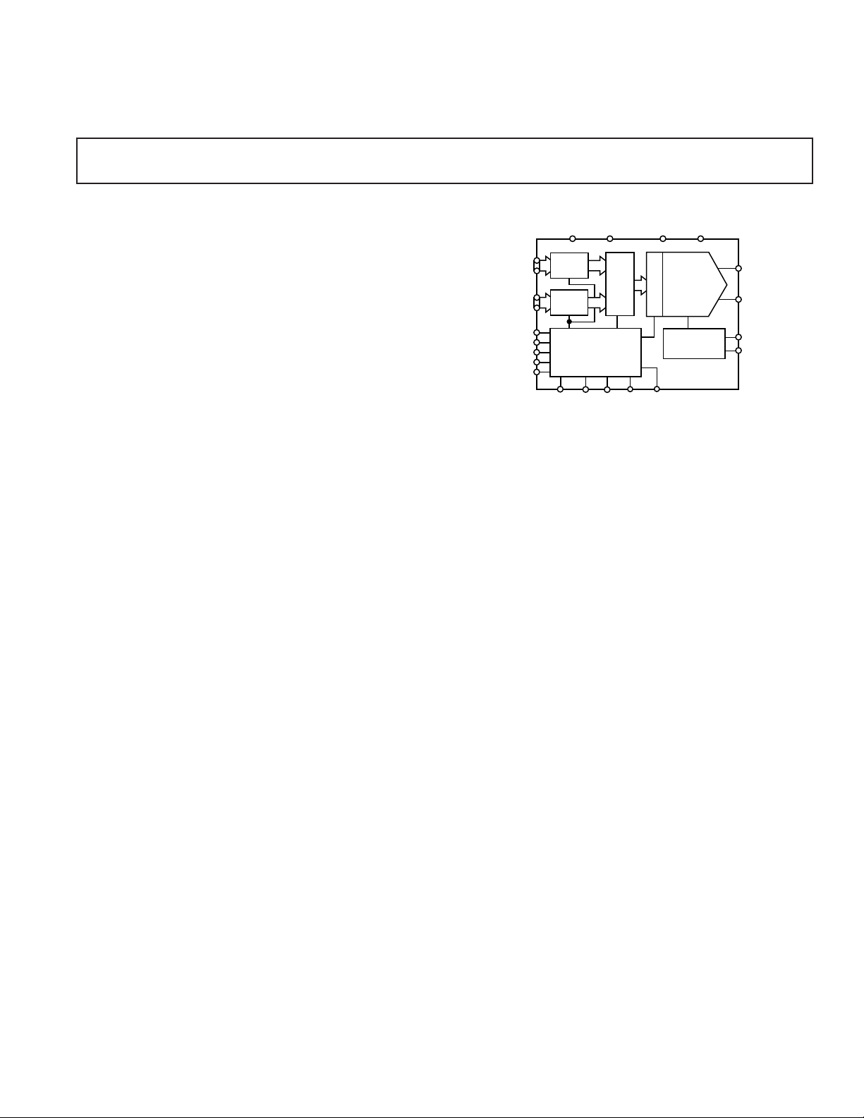
FUNCTIONAL BLOCK DIAGRAM
PORT1
PORT2
CLK+
CLK–
CLKVDD
PLLVDD
CLKCOM
DVDD
DCOM
LATCH
LATCH
PLL
CLOCK
MULTIPLIER
RESET LPF DIV0 DIV1 PLLLOCK
AVDD ACOM
MUX
DAC LATCH
REFERENCE
AD9751
DAC
AD9751
The DAC utilizes a segmented current source architecture combined with a proprietary switching technique to reduce glitch
energy and maximize dynamic accuracy. Differential current
outputs support single-ended or differential applications. The
differential outputs each provide a nominal full-scale current
from 2 mA to 20 mA.
The AD9751 is manufactured on an advanced low cost 0.35 µm
CMOS process. It operates from a single supply of 3.0 V to 3.6 V
and consumes 155 mW of power.
PRODUCT HIGHLIGHTS
1. The AD9751 is a member of a pin compatible family of high
speed TxDAC+s, providing 10-, 12-, and 14-bit resolution.
2. Ultrahigh Speed 300 MSPS Conversion Rate.
3. Dual 10-Bit Latched, Multiplexed Input Ports. The AD9751
features a flexible digital interface allowing high speed data
conversion through either a single or dual port input.
4. Low Power. Complete CMOS DAC function operates on
155 mW from a 3.0 V to 3.6 V single supply. The DAC fullscale current can be reduced for lower power operation.
5. On-Chip Voltage Reference. The AD9751 includes a 1.20 V
temperature compensated band gap voltage reference.
*Protected by U.S. Patent numbers 5450084, 5568145, 5689257, and 5703519.
Other patents pending.
REV. C
Information furnished by Analog Devices is believed to be accurate and
reliable. However, no responsibility is assumed by Analog Devices for its
use, nor for any infringements of patents or other rights of third parties that
may result from its use. No license is granted by implication or otherwise
under any patent or patent rights of Analog Devices. Trademarks and
registered trademarks are the property of their respective companies.
One Technology Way, P.O. Box 9106, Norwood, MA 02062-9106, U.S.A.
Tel: 781/329-4700 www.analog.com
Fax: 781/326-8703 © 2003 Analog Devices, Inc. All rights reserved.

AD9751–SPECIFICATIONS
DC SPECIFICATIONS
(T
to T
MIN
, AVDD = DVDD = PLLVDD = CLKVDD = 3.3 V, I
MAX
= 20 mA, unless otherwise noted.)
OUTFS
Parameter Min Typ Max Unit
RESOLUTION 10 Bits
DC ACCURACY
1
Integral Linearity Error (INL) –1 ±0.3 +1 LSB
Differential Nonlinearity (DNL) –0.5 ± 0.2 +0.5 LSB
ANALOG OUTPUT
Offset Error –0.025 ±0.01 +0.025 % of FSR
Gain Error (Without Internal Reference) –5 ±0.5 +2 % of FSR
Gain Error (With Internal Reference) –7 ±0.25 +2 % of FSR
Full-Scale Output Current
2
2.0 20.0 mA
Output Compliance Range –1.0 +1.25 V
Output Resistance 100 kΩ
Output Capacitance 5 pF
REFERENCE OUTPUT
Reference Voltage 1.14 1.20 1.26 V
Reference Output Current
3
100 nA
REFERENCE INPUT
Input Compliance Range 0.1 1.25 V
Reference Input Resistance 1 MΩ
TEMPERATURE COEFFICIENTS
Offset Drift 0 ppm of FSR/°C
Gain Drift (Without Internal Reference) ±50 ppm of FSR/°C
Gain Drift (With Internal Reference) ±100 ppm of FSR/°C
Reference Voltage Drift ±50 ppm/°C
POWER SUPPLY
Supply Voltages
AVDD 3.0 3.3 3.6 V
DVDD 3.0 3.3 3.6 V
PLLVDD 3.0 3.3 3.6 V
CLKVDD 3.0 3.3 3.6 V
Analog Supply Current (I
Digital Supply Current (I
PLL Supply Current (I
Clock Supply Current (I
Power Dissipation
Power Dissipation
4
(3 V, I
5
(3 V, I
PLLVDD
Power Supply Rejection Ratio
4
)
AVDD
4
)
DVDD
4
)
4
)
CLKVDD
= 20 mA) 155 165 mW
OUTFS
= 20 mA) 216 mW
OUTFS
6
—AVDD –0.1 +0.1 % of FSR/V
33 36 mA
3.5 4.5 mA
4.5 5.1 mA
10.0 11.5 mA
Power Supply Rejection Ratio6—DVDD –0.04 +0.04 % of FSR/V
OPERATING RANGE –40 +85 °C
NOTES
1
Measured at I
2
Nominal full-scale current, I
3
An external buffer amplifier is recommended to drive any external load.
4
100 MSPS f
5
300 MSPS f
6
±5% power supply variation.
Specifications subject to change without notice.
, driving a virtual ground.
OUTA
with PLL on, f
DAC
.
DAC
OUTFS
, is 32× the I
= 1 MHz, all supplies = 3.0 V.
OUT
current.
REF
–2–
REV. C

AD9751
(T
to T
, AVDD = DVDD = CLKVDD = 3.3 V, PLLVDD = 0 V, I
MAX
DYNAMIC SPECIFICATIONS
MIN
Transformer-Coupled Output, 50 ⍀ Doubly Terminated, unless otherwise noted.)
Parameter Min Typ Max Unit
DYNAMIC PERFORMANCE
Maximum Output Update Rate (f
Output Settling Time (t
Output Propagation Delay (t
Glitch Impulse
1
) (to 0.1%)
ST
PD
Output Rise Time (10% to 90%)
Output Fall Time (90% to 10%)
Output Noise (I
Output Noise (I
= 20 mA) 50 pA/√Hz
OUTFS
= 2 mA) 30 pA/√Hz
OUTFS
) 300 MSPS
DAC
1
1
)
1
1
11 ns
1ns
5 pV-s
2.5 ns
2.5 ns
AC LINEARITY
Spurious-Free Dynamic Range to Nyquist
= 100 MSPS; f
f
DAC
= 1.00 MHz
OUT
0 dBFS Output 70 80 dBc
–6 dBFS Output 72 dBc
–12 dBFS Output 72 dBc
= 65 MSPS; f
f
DATA
= 65 MSPS; f
f
DATA
f
= 65 MSPS; f
DATA
= 65 MSPS; f
f
DATA
= 65 MSPS; f
f
DATA
f
= 200 MSPS; f
DAC
= 200 MSPS; f
f
DAC
= 200 MSPS; f
f
DAC
f
= 200 MSPS; f
DAC
= 200 MSPS; f
f
DAC
= 300 MSPS; f
f
DAC
f
= 300 MSPS; f
DAC
= 300 MSPS; f
f
DAC
= 300 MSPS; f
f
DAC
f
= 300 MSPS; f
DAC
= 1.1 MHz
OUT
= 5.1 MHz
OUT
= 10.1 MHz
OUT
= 20.1 MHz
OUT
= 30.1 MHz
OUT
= 1.1 MHz 74 dBc
OUT
= 11.1 MHz 71 dBc
OUT
= 31.1 MHz 66 dBc
OUT
= 51.1 MHz 66 dBc
OUT
= 71.1 MHz 63 dBc
OUT
= 1.1 MHz 74 dBc
OUT
= 26.1 MHz 71 dBc
OUT
= 51.1 MHz 66 dBc
OUT
= 101.1 MHz 66 dBc
OUT
= 141.1 MHz 63 dBc
OUT
2
2
2
2
2
73 dBc
73 dBc
72 dBc
68 dBc
64 dBc
Spurious-Free Dynamic Range within a Window
= 100 MSPS; f
f
DAC
= 1 MHz; 2 MHz Span
OUT
0 dBFS 81 91 dBc
= 65 MSPS; f
f
DAC
= 150 MSPS; f
f
DAC
= 5.02 MHz; 2 MHz Span 81 dBc
OUT
= 5.04 MHz; 4 MHz Span 81 dBc
OUT
Total Harmonic Distortion
= 100 MSPS; f
f
DAC
= 1.00 MHz
OUT
0 dBFS –80 –69 dBc
= 65 MHz; f
f
DAC
= 150 MHz; f
f
DAC
= 2.00 MHz –72 dBc
OUT
= 2.00 MHz –72 dBc
OUT
Multitone Power Ratio (Eight Tones at 110 kHz Spacing)
= 65 MSPS; f
f
DAC
= 2.00 MHz to 2.77 MHz
OUT
0 dBFS Output 69 dBc
–6 dBFS Output 67 dBc
–12 dBFS Output 65 dBc
NOTES
1
Measured single-ended into 50 Ω load.
2
Single-Port Mode (PLL disabled, DIV0 = 1, DIV1 = 0, data on Port 1).
Specifications subject to change without notice.
= 20 mA, Differential
OUTFS
REV. C
–3–

AD9751
DIGITAL SPECIFICATIONS
(T
to T
MIN
, AVDD = DVDD = PLLVDD = CLKVDD = 3.3 V, I
MAX
= 20 mA, unless otherwise noted.)
OUTFS
Parameter Min Typ Max Unit
DIGITAL INPUTS
Logic 1 2.1 3 V
Logic 0 0 0.9 V
Logic 1 Current –10 +10 µA
Logic 0 Current –10 +10 µA
Input Capacitance 5 pF
Input Setup Time (t
Input Hold Time (t
Latch Pulsewidth (t
Input Setup Time (t
Input Hold Time (t
CLK to PLLLOCK Delay (t
Latch Pulsewidth (t
PLLOCK (V
OH
), TA = 25°C 1.0 0.5 ns
S
), TA = 25°C 1.0 0.5 ns
H
), TA = 25°C 1.5 ns
LPW
PLLVDD = 0 V), TA = 25°C –1.0 –1.5 ns
S,
PLLVDD = 0 V), TA = 25°C 2.5 1.7 ns
H,
LPW
, PLLVDD = 0 V), TA = 25°C 3.5 4.0 ns
D
PLLVDD = 0 V), TA = 25°C 1.5 ns
) 3.0 V
PLLOCK (VOL) 0.3 V
CLK INPUTS
Input Voltage Range 0 3 V
Common-Mode Voltage 0.75 1.5 2.25 V
Differential Voltage 0.5 1.5 V
Min CLK Frequency* 6.25 MHz
*Min CLK Frequency applies only when using internal PLL. When PLL is disabled, there is no minimum CLK frequency.
Specifications subject to change without notice.
–4–
REV. C
AD9751
ABSOLUTE MAXIMUM RATINGS*
Parameter With Respect to Min Max Unit
AVDD, DVDD, CLKVDD, PLLVDD ACOM, DCOM, CLKCOM, PLLCOM –0.3 +3.9 V
AVDD, DVDD, CLKVDD, PLLVDD AVDD, DVDD, CLKVDD, PLLVDD –3.9 +3.9 V
ACOM, DCOM, CLKCOM, PLLCOM ACOM, DCOM, CLKCOM, PLLCOM –0.3 +0.3 V
REFIO, REFLO, FSADJ ACOM –0.3 AVDD + 0.3 V
, I
I
OUTA
OUTB
Digital Data Inputs (DB9 to DB0) DCOM –0.3 DVDD + 0.3 V
CLK+/CLK–, PLLLOCK CLKCOM –0.3 CLKVDD + 0.3 V
DIV0, DIV1, RESET CLKCOM –0.3 CLKVDD + 0.3 V
LPF PLLCOM –0.3 PLLVDD + 0.3 V
Junction Temperature 150 °C
Storage Temperature –65 +150 °C
Lead Temperature (10 sec) 300 °C
*Stresses above those listed under Absolute Maximum Ratings may cause permanent damage to the device. This is a stress rating only; functional operation of the device
at these or any other conditions above those indicated in the operational sections of this specification is not implied. Exposure to absolute maximum ratings for extended
periods may affect device reliability.
t
t
H
S
ACOM –1.0 AVDD + 0.3 V
ORDERING GUIDE
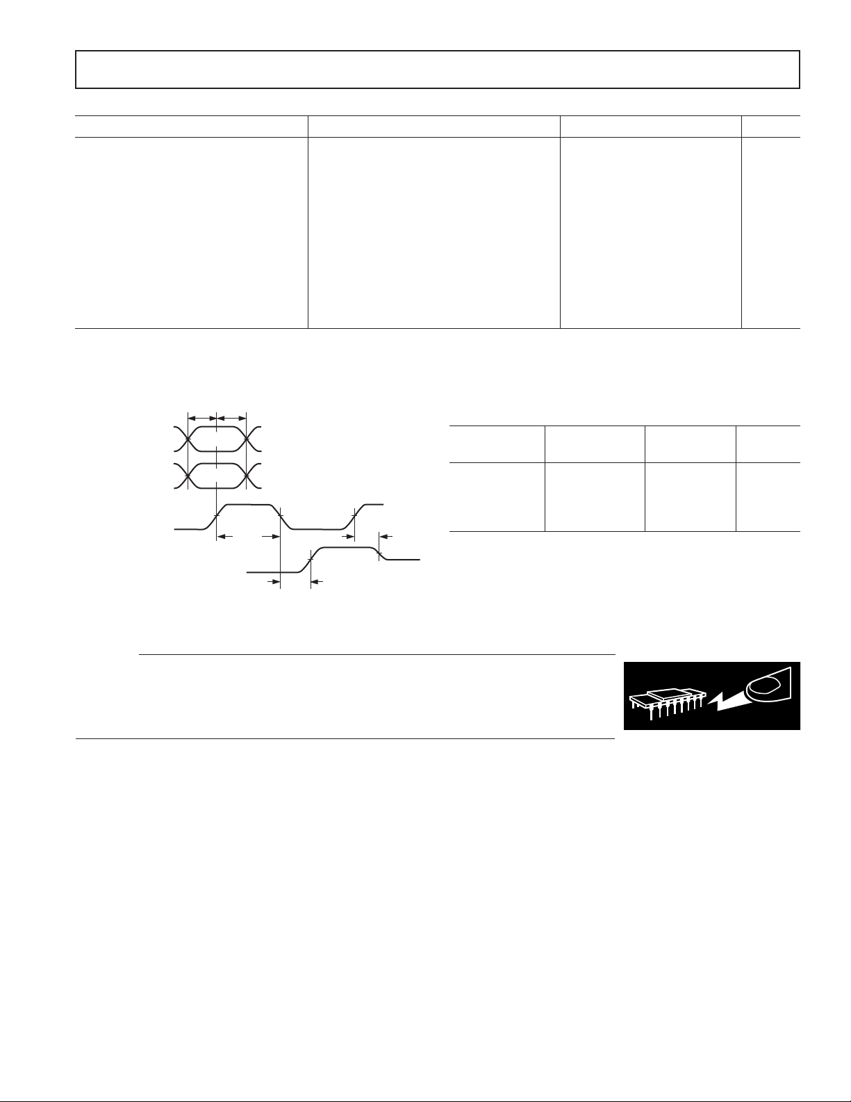
PORT 1
DATA IN
PORT 2
DATA X
DATA Y
Model Range Description Option
AD9751AST –40°C to +85°C 48-Lead LQFP ST-48
Temperature Package Package
AD9751ASTRL –40°C to +85°C 48-Lead LQFP ST-48
AD9751-EB Evaluation
INPUT CLK
(PLL ENABLED)
OR I
I
OUTA
OUTB
t
LPW
t
PD
DATA X
t
PD
DATA Y
THERMAL CHARACTERISTIC
Thermal Resistance
θJA = 91°C/W
Figure 1. I/O Timing
CAUTION
ESD (electrostatic discharge) sensitive device. Electrostatic charges as high as 4000 V readily
accumulate on the human body and test equipment and can discharge without detection. Although
the AD9751 features proprietary ESD protection circuitry, permanent damage may occur on
devices subjected to high energy electrostatic discharges. Therefore, proper ESD precautions are
recommended to avoid performance degradation or loss of functionality.
Board
WARNING!
ESD SENSITIVE DEVICE
REV. C
–5–

AD9751
PIN CONFIGURATION
LPF
CLKCOM
ACOM
AD9751
TOP VIEW
(Not to Scale)
LSB–P1B0
RESERVED
OUTAIOUTB
I
AVDD
RESERVED
RESERVED
RESERVED
FSADJ
REFIO
DVDD
DCOM
DIV1
DIV0
36
RESERVED
35
RESERVED
34
RESERVED
33
RESERVED
32
P2B0–LSB
31
P2B1
30
P2B2
29
P2B3
28
P2B4
27
P2B5
26
P2B6
25
P2B7
RESERVED = NO
USER CONNECTIONS
P2B8
MSB–P2B9
MSB–P1B9
RESET
CLK+
CLK–
DCOM
DVDD
PLLLOCK
P1B8
P1B7
P1B6
P1B5
P1B4
CLKVDD
PLLVDD
48 47 46 45 44 39 38 3743 42 41 40
1
PIN 1
2
IDENTIFIER
3
4
5
6
7
8
9
10
11
12
13 14 15 16 17 18 19 20 21 22 23 24
P1B3
P1B2
P1B1
PIN FUNCTION DESCRIPTIONS
Pin No. Mnemonic Description
1 RESET Internal Clock Divider Reset
2 CLK+ Differential Clock Input
3 CLK– Differential Clock Input
4, 22 DCOM Digital Common
5, 21 DVDD Digital Supply Voltage
6PLLLOCK Phase-Locked Loop Lock Indicator Output
7–16 P1B9–P1B0 Data Bits P1B9 to P1B0, Port 1
17–20, 33–36 RESERVED
23–32 P2B9–P2B0 Data Bits P2B9 to P2B0, Port 2
37, 38 DIV0, DIV1 Control Inputs for PLL and Input Port Selector Mode; see Tables I and II for details.
39 REFIO Reference Input/Output
40 FSADJ Full-Scale Current Output Adjust
41 AVDD Analog Supply Voltage
42 I
43 I
OUTB
OUTA
Differential DAC Current Output
Differential DAC Current Output
44 ACOM Analog Common
45 CLKCOM Clock and Phase-Locked Loop Common
46 LPF Phase-Locked Loop Filter
47 PLLVDD Phase-Locked Loop Supply Voltage
48 CLKVDD Clock Supply Voltage
–6–
REV. C
AD9751
TERMINOLOGY
Linearity Error (Also Called Integral Nonlinearity or INL)
Linearity error is defined as the maximum deviation of the actual
analog output from the ideal output, determined by a straight
line drawn from zero to full scale.
Differential Nonlinearity (DNL)
DNL is the measure of the variation in analog value, normalized
to full scale, associated with a 1 LSB change in digital input code.
Monotonicity
A D/A converter is monotonic if the output either increases or
remains constant as the digital input increases.
Offset Error
The deviation of the output current from the ideal of zero is
called offset error. For I
inputs are all 0s. For I
, 0 mA output is expected when the
OUTA
, 0 mA output is expected when the
OUTB
inputs are all 1s.
Gain Error
The difference between the actual and ideal output span. The
actual span is determined by the output when all inputs are set
to 1s minus the output when all inputs are set to 0s.
Output Compliance Range
The range of allowable voltage at the output of a current-output
DAC. Operation beyond the maximum compliance limits may
cause either output stage saturation or breakdown, resulting in
nonlinear performance.
Temperature Drift
Specified as the maximum change from the ambient (25°C)
value to the value at either T
MIN
or T
. For offset and gain
MAX
drift, the drift is reported in ppm of full-scale range (FSR) per
degree C. For reference drift, the drift is reported in ppm per
degree C.
Power Supply Rejection
The maximum change in the full-scale output as the supplies
are varied from minimum to maximum specified voltages.
Settling Time
The time required for the output to reach and remain within a
specified error band around its final value, measured from the
start of the output transition.
Glitch Impulse
Asymmetrical switching times in a DAC cause undesired output
transients that are quantified by a glitch impulse. It is specified
as the net area of the glitch in pV-s.
Spurious-Free Dynamic Range
The difference, in dB, between the rms amplitude of the output
signal and the peak spurious signal over the specified bandwidth.
Total Harmonic Distortion (THD)
THD is the ratio of the rms sum of the first six harmonic components to the rms value of the measured fundamental. It is
expressed as a percentage or in decibels (dB).
Signal-to-Noise Ratio (SNR)
SNR is the ratio of the rms value of the measured output signal
to the rms sum of all other spectral components below the
Nyquist frequency, excluding the first six harmonics and dc.
The value for SNR is expressed in decibels.
Adjacent Channel Power Ratio (ACPR)
A ratio in dBc between the measured power within a channel
relative to its adjacent channel.
0.1F
R
SET
2k⍀
1.2V REF
REFIO
FSADJ
DCOM
AD9751
ACOM
3.0V TO 3.6V
DVDD
AVDD
PMOS CURRENT
SOURCE ARRAY
I
SEGMENTED
SWITCHES FOR
DB0 TO DB9
DAC LATCH
2–1 MUX
PORT 1 LATCH
DB0 – DB9
DIGITAL DATA INPUTS
TEKTRONIX DG2020
AWG2021 w/OPTION 4
LECROY 9210
PULSE GENERATOR
(FOR DATA RETIMING)
PORT 2 LATCH
OR
DAC
DB0 – DB9
CLK+
MINI
CIRCUITS
T1-1T
PLL ENABLED
PLL DISABLED
PLL
CIRCUITRY
CLK–
OUTA
I
OUTB
PLLVDD
CLKVDD
RESET
LPF
CLKCOM
DIV0
DIV1
PLLLOCK
1k⍀
1k⍀
HP8644
SIGNAL
GENERATOR
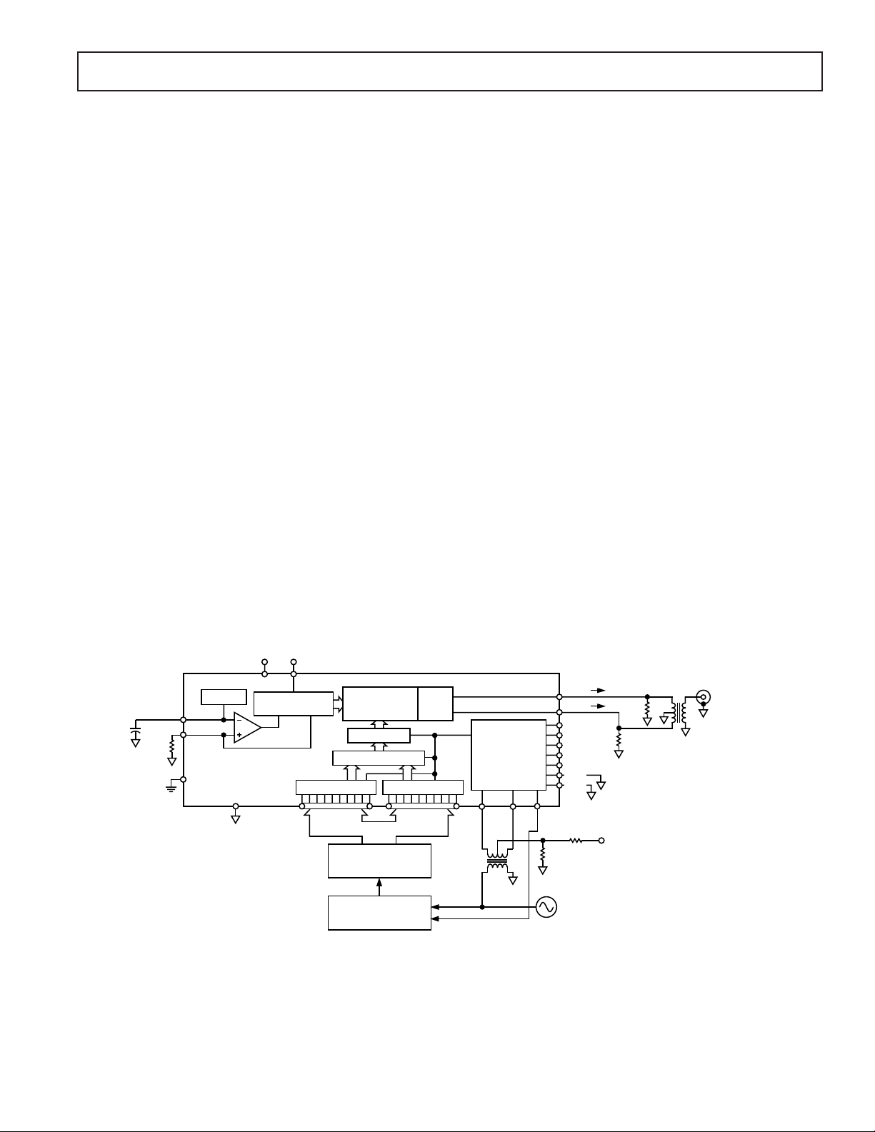
Figure 2. Basic AC Characterization Test Setup
50⍀
50⍀
3.0V TO 3.6V
MINI
CIRCUITS
T1-1T
TO ROHDE &
SCHWARZ
FSEA30
SPECTRUM
ANALYZER
REV. C
–7–
AD9751–Typical Performance Characteristics
f
OUT
(MHz)
90
70
40
1000
SFDR (dBc)
80
60
50
20 40 60 80 120 140 160
SFDR NEAR CARRIERS
(2F1-F2, 2F2-F1)
SFDR OVER NYQUIST BAND
A
OUT
(dBm)
90
70
40
–6–16
SFDR (dBc)
80
60
50
–14 –12 –10 –8 –4 –2 0–18–20
18.18/19.18MHz
@ 200MSPS
11.82/12.82MHz
@ 130MSPS
27.27/28.27MHz
@ 300MSPS
90
80
70
–6dBFS
60
SFDR (dBc)
50
40
0dBFS
–12dBFS
10 15 20 25 30
f
(MHz)
OUT
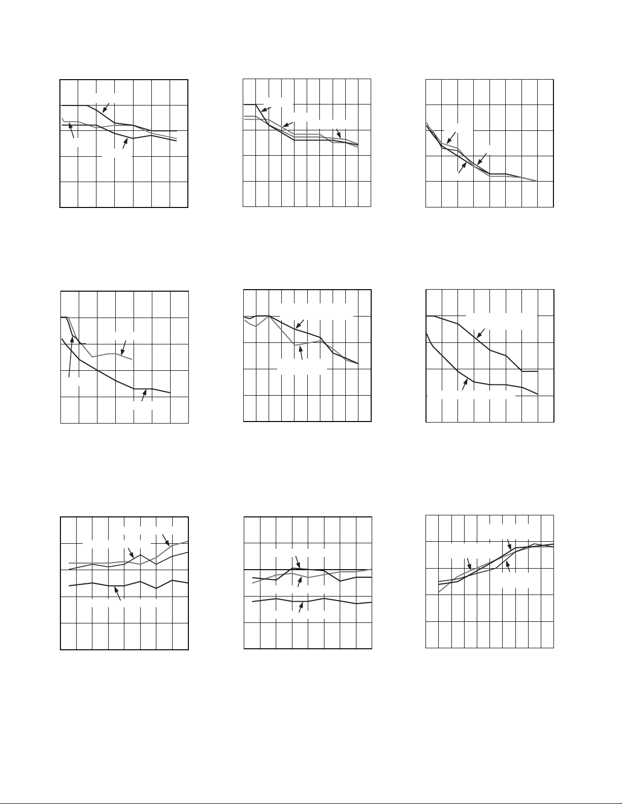
TPC 1. Single-Tone SFDR vs. f
= 65 MSPS; Single Port Mode
f
DAC
90
80
70
60
SFDR (dBc)
65MSPS
50
40
20 40 60 80 120 140
TPC 4. SFDR vs. f
200MSPS
f
(MHz)
OUT
300MSPS
1000
@ 0 dBFS
OUT
OUT
3550
@
90
80
70
60
SFDR (dBc)
50
40
0dBFS
–6dBFS
20 30 40 50 60 70 80 90
f
OUT
–12dBFS
(MHz)
TPC 2. Single-Tone SFDR vs. f
@ f
= 200 MSPS
DAC
90
SFDR NEAR CARRIERS
80
70
60
SFDR (dBc)
50
40
(2F1-F2, 2F2-F1)
SFDR OVER
NYQUIST BAND
20 30 40 50 60 70 80 90
f
(MHz)
OUT
TPC 5. Two-Tone IMD vs. f
f
= 200 MSPS, 1 MHz Spacing
DAC
between Tones, 0 dBFS
OUT
100100
OUT
100100
@
90
80
–12dBFS
70
60
SFDR (dBc)
0dBFS
50
40
20 40 60 80 120 140 160
–6dBFS
f
OUT
1000
(MHz)
TPC 3. Single-Tone SFDR vs. f
f
= 300 MSPS
DAC
TPC 6. Two-Tone IMD vs. f
= 300 MSPS, 1 MHz Spacing
f
DAC
between Tones, 0 dBFS
OUT
OUT
@
@
90
80
70
60
SFDR (dBc)
50
40
TPC 7. Single-Tone SFDR vs. A
f
= f
OUT
18.18MHz @ 200MSPS
27.27MHz @ 300MSPS
–14 –12 –10 –8 –4 –2 0
/11
DAC
11.82MHz @ 130MSPS
–6–16
A
(dB)
OUT
OUT
@
90
80
70
60
SFDR (dBc)
50
40
40MHz @ 200MSPS
26MHz @ 130MSPS
60MHz @ 300MSPS
–14 –12 –10 –8 –4 –2 0
–6–16
A
(dBm)
OUT
TPC 8. Single-Tone SFDR vs. A
@ f
= f
DAC
/5
OUT
–8–
OUT
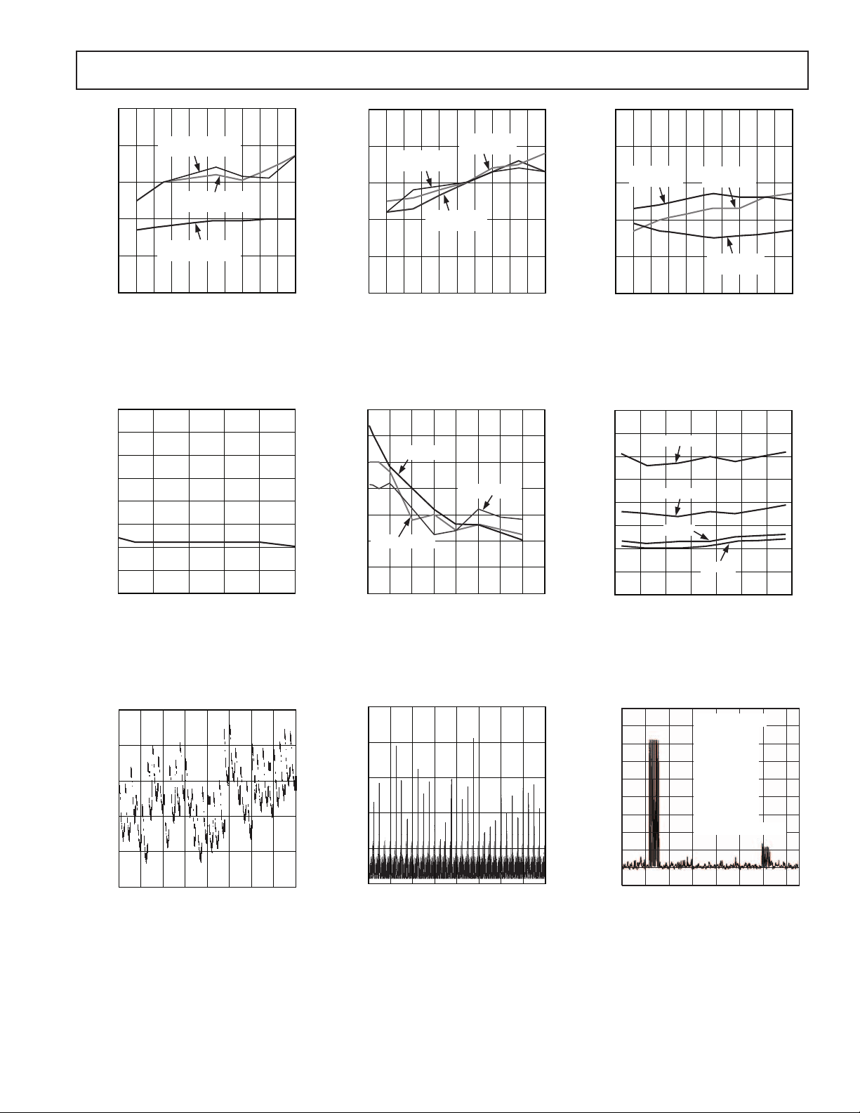
TPC 9. Two-Tone IMD (Third Order
Products) vs. A
OUT
@ f
OUT
= f
DAC
/11
REV. C
AD9751
)
90
80
70
60
SFDR (dBc)
50
40
18.18MHz/19.18MHz
@ 200MSPS
11.82MHz/12.82MHz
@ 130MSPS
27.27MHz/28.27MHz
@ 300MSPS
–14 –12 –10 –8 –4 –2 0–18–20
A
(dBm)
OUT
–6–16
TPC 10. Two-Tone IMD (to Nyquist)
vs. A
TPC 13. SINAD vs. f
@ f
OUT
90
85
80
75
70
65
SINAD (dBm)
60
55
50
= f
f
DAC
DAC
(MHz)
/11
DAC
@ f
OUT
OUT
100 150 200 250
30050
=
10 MHz, 0 dBFS
90
80
70
60
SFDR (dBc)
50
40
60MHz/61MHz
@ 300MSPS
–14 –12 –10 –8 –4 –2 0–18–20
26MHz/27MHz
@ 130MSPS
40MHz/41MHz
@ 200MSPS
A
(dBm)
OUT
–6–16
TPC 11. Two-Tone IMD (Third Order
Products) vs. A
75
70
I
OUTFS
65
60
55
SFDR (dBc)
50
I
= 10mA
OUTFS
45
40
TPC 14. SFDR vs. I
@ f
OUT
= 20mA
40 60 80 100 120
f
OUT
OUT
I
OUTFS
(MHz)
OUTFS
= f
= 5mA
, f
DAC
DAC
140
=
/5
160200
300 MSPS @ 0 dBFS
90
80
26MHz/27MHz
70
60
SFDR (dBc)
50
40
@ 130MSPS
–14 –12 –10 –8 –4 –2 0–18–20
40MHz/41MHz
@ 200MSPS
60MHz/61MHz
A
(dBm)
OUT
@ 300MSPS
–6–16
TPC 12. Two-Tone IMD (to Nyquist)
vs. A
OUT
80
75
70
65
60
SFDR (dBc)
55
50
45
40
@ f
= f
OUT
10MHz
40MHz
80MHz
–10 10 30 50
TEMPERATURE (ⴗC
DAC
120MHz
/5
90–30–50
70
TPC 15. SFDR vs. Temperature,
f
= 300 MSPS @ 0 dBFS
DAC
0.10
0.05
INL (LSB)
–0.05
–0.10
–0.15
REV. C
0
255 383 511 767
TPC 16. Typical INL
CODE
639
895
0.18
0.14
0.10
DNL (LSB)
0.06
0.02
10241270
–0.02
255 383 511 767
639
CODE
895
10241270
TPC 17. Typical DNL
0
–10
–20
–30
–40
–50
–60
AMPLITUDE (dBm)
–70
–80
–90
–100
200
f
= 300MSPS
DAC
= 24MHz
f
OUT1
= 25MHz
f
OUT2
= 26MHz
f
OUT3
= 27MHz
f
OUT4
f
= 28MHz
OUT5
= 29MHz
f
OUT6
= 30MHz
f
OUT7
= 31MHz
f
OUT8
SFDR = 58dBc
MAGNITUDE = 0dBFS
40 60 100 120
80
FREQUENCY (MHz)
TPC 18. Eight-Tone SFDR @ f
f
DAC
/11, f
= 300 MSPS
DAC
OUT
140
≈
–9–
 Loading...