10-Bit, 210 MSPS TxDAC® D/A Converter
FEATURES
High performance member of pin-compatible
TxDAC product family
Excellent spurious-free dynamic range performance
SNR @ 5 MHz output, 125 MSPS: 65 dB
Twos complement or straight binary data format
Differential current outputs: 2 mA to 20 mA
Power dissipation: 135 mW @ 3.3 V
Power-down mode: 15 mW @ 3.3 V
On-chip 1.2 V Reference
CMOS-compatible digital interface
28-lead SOIC, 28-lead TSSOP, and 32-lead LFCSP
packages
Edge-triggered latches
APPLICATIONS
Wideband communication transmit channel
Direct IF
Base stations
Wireless local loops
Digital radio links
Direct digital synthesis (DDS)
Instrumentation
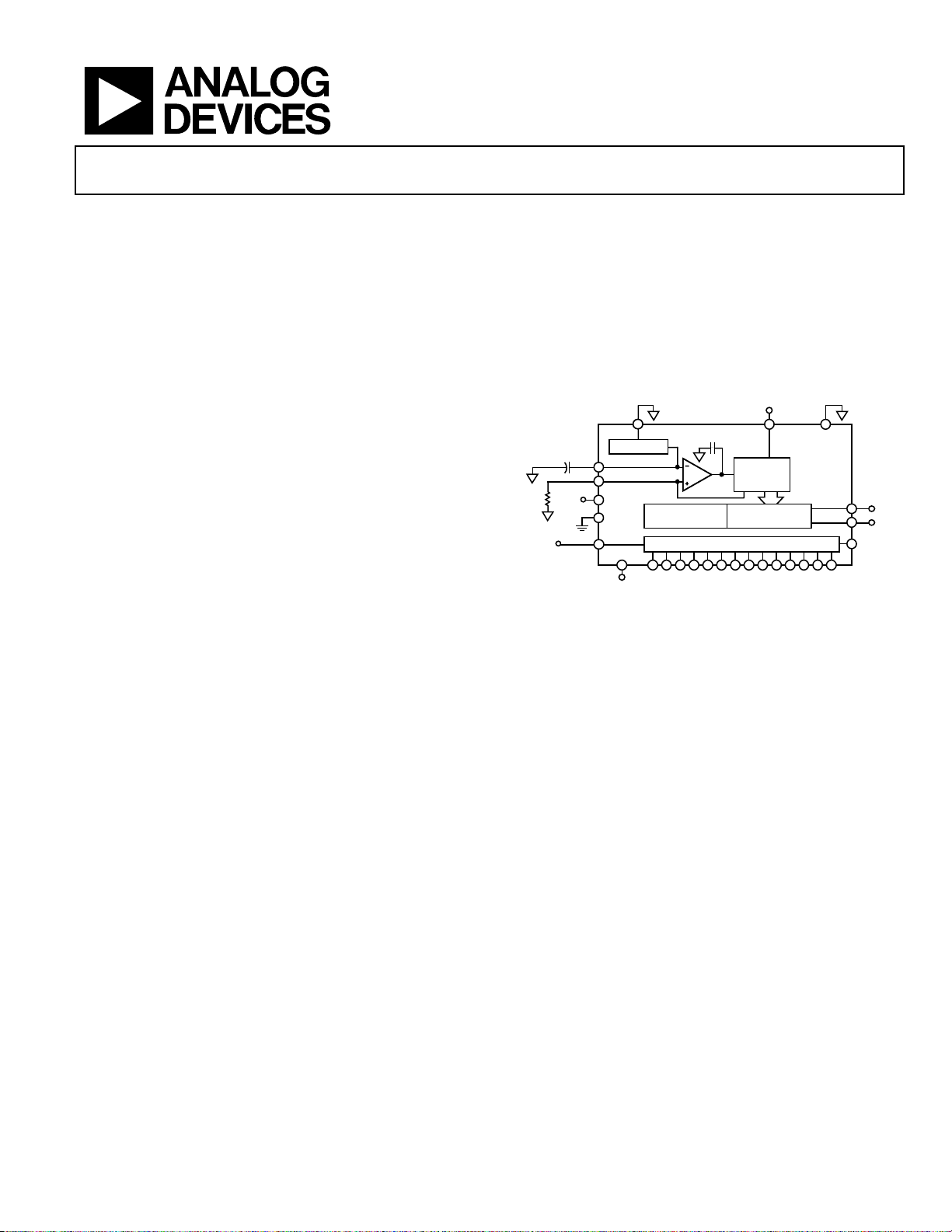
FUNCTIONAL BLOCK DIAGRAM
3.3V
R
SET
CLOCK
0.1μF
3.3V
1.2V REF
REFIO
FS ADJ
DVDD
DCOM
CLOCK
SLEEP
REFLO
150pF
SEGMENTED
SWITCHES
LATCHES
DIGITAL DATA INPUTS (DB9–DB0)
Figure 1.
AVDD ACOM
CURRENT
SOURCE
ARRAY
LSB
SWITCHES
AD9740
AD9740
IOUTA
IOUTB
MODE
02911-001
GENERAL DESCRIPTION
The AD97401 is a 10-bit resolution, wideband, third generation
member of the TxDAC series of high performance, low power
CMOS digital-to-analog converters (DACs). The TxDAC
family, consisting of pin-compatible 8-, 10-, 12-, and 14-bit
DACs, is specifically optimized for the transmit signal path
of communication systems. All of the devices share the same
interface options, small outline package, and pinout, providing
an upward or downward component selection path based
on performance, resolution, and cost. The AD9740 offers
exceptional ac and dc performance while supporting update
rates up to 210 MSPS.
The AD9740’s low power dissipation makes it well suited for
portable and low power applications. Its power dissipation
can be further reduced to 60 mW with a slight degradation in
performance by lowering the full-scale current output. In
addition, a power-down mode reduces the standby power
dissipation to approximately 15 mW. A segmented current
source architecture is combined with a proprietary switching
technique to reduce spurious components and enhance
dynamic performance.
Edge-triggered input latches and a 1.2 V temperature-compensated
band gap reference have been integrated to provide a complete
monolithic DAC solution. The digital inputs support 3 V CMOS
logic families.
PRODUCT HIGHLIGHTS
1. The AD9740 is the 10-bit member of the pin-compatible
TxDAC family, which offers excellent INL and DNL
performance.
2. Data input supports twos complement or straight binary
data coding.
3. High speed, single-ended CMOS clock input supports
210 MSPS conversion rate.
4. Low power: Complete CMOS DAC function operates on
135 mW from a 2.7 V to 3.6 V single supply. The DAC fullscale current can be reduced for lower power operation,
and a sleep mode is provided for low power idle periods.
5. On-chip voltage reference: The AD9740 includes a 1.2 V
temperature-compensated band gap voltage reference.
6. Industry-standard 28-lead SOIC, 28-lead TSSOP, and 32-
lead LFCSP packages.
1
Protected by U.S. Patent Numbers 5568145, 5689257, and 5703519.
Rev. B
Information furnished by Analog Devices is believed to be accurate and reliable. However, no
responsibility is assumed by Anal og Devices for its use, nor for any infringements of patents or ot her
rights of third parties that may result from its use. Specifications subject to change without notice. No
license is granted by implication or otherwise under any patent or patent rights of Analog Devices.
Trademarks and registered trademarks are the property of their respective owners.
One Technology Way, P.O. Box 9106, Norwood, MA 02062-9106, U.S.A.
Tel: 781.329.4700 www.analog.com
Fax: 781.461.3113 © 2005 Analog Devices, Inc. All rights reserved.

AD9740
TABLE OF CONTENTS
Features .............................................................................................. 1
DAC Transfer Function ............................................................. 14
Applications....................................................................................... 1
Functional Block Diagram .............................................................. 1
General Description......................................................................... 1
Product Highlights........................................................................... 1
Revision History ............................................................................... 3
Specifications..................................................................................... 4
DC Specifications ......................................................................... 4
Dynamic Specifications ............................................................... 5
Digital Specifications ................................................................... 6
Absolute Maximum Ratings............................................................ 7
Thermal Characteristics .............................................................. 7
ESD Caution.................................................................................. 7
Pin Configurations and Function Descriptions ........................... 8
Te r mi n ol o g y ...................................................................................... 9
Typical Performance Characteristics ........................................... 10
Functional Description ..................................................................13
Reference Operation ..................................................................13
Analog Outputs .......................................................................... 14
Digital Inputs .............................................................................. 15
Clock Input.................................................................................. 15
DAC Timing................................................................................ 16
Power Dissipation....................................................................... 16
Applying the AD9740 ................................................................ 17
Differential Coupling Using a Transformer............................... 17
Differential Coupling Using an Op Amp................................ 18
Single-Ended, Unbuffered Voltage Output............................. 18
Single-Ended, Buffered Voltage Output Configuration........ 18
Power and Grounding Considerations, Power Supply
Rejection...................................................................................... 19
Evaluation Board ............................................................................ 20
General Description................................................................... 20
Outline Dimensions ....................................................................... 30
Ordering Guide .......................................................................... 31
Reference Control Amplifier .................................................... 14
Rev. B | Page 2 of 32

AD9740
REVISION HISTORY
12/05—Rev. A to Rev. B
Updated Format.................................................................. Universal
Changes to General Description and Product Highlights...........1
Changes to Table 1 ............................................................................4
Changes to Table 2 ............................................................................5
Changes to Table 5 ............................................................................8
Changes to Figure 6.........................................................................10
Inserted Figure 11; Renumbered Sequentially ............................10
Changes to Figure 12, Figure 13, Figure 14, and Figure 15 .......11
Changes to Functional Description and Reference
Operation Sections..........................................................................13
Inserted Figure 23; Renumbered Sequentially ............................13
Changes to DAC Transfer Function Section and Figure 25 ......14
Changes to Digital Inputs Section.................................................15
Changes to Figure 30 and Figure 31 .............................................17
Updated Outline Dimensions........................................................30
Changes to Ordering Guide...........................................................31
5/03—Rev. 0 to Rev. A
Added 32-Lead LFCSP Package....................................... Universal
Edits to Features ................................................................................1
Edits to Product Highlights ............................................................. 1
Edits to DC Specifications ...............................................................2
Edits to Dynamic Specifications .....................................................3
Edits to Digital Specifications..........................................................4
Edits to Absolute Maximum Ratings..............................................5
Edits to Thermal Characteristics ....................................................5
Edits to Ordering Guide................................................................... 5
Edits to Pin Configuration...............................................................6
Edits to Pin Function Descriptions ................................................6
Edits to Figure 2 ................................................................................7
Replaced TPCs 1, 4, 7, and 8............................................................ 8
Edits to Figure 3 ..............................................................................10
Edits to Functional Description Section ......................................10
Edits to Digital Inputs Section.......................................................12
Added Clock Input Section............................................................12
Added Figure 7 ................................................................................12
Edits to DAC Timing Section........................................................12
Edits to Sleep Mode Operation Section .......................................13
Edits to Power Dissipation Section...............................................13
Renumbered Figures 8 to 26..........................................................13
Added Figure 11..............................................................................13
Added Figures 27 to 35...................................................................21
Updated Outline Dimensions........................................................26
5/02—Revision 0: Initial Version
Rev. B | Page 3 of 32

AD9740
SPECIFICATIONS
DC SPECIFICATIONS
T
to T
MIN
Table 1.
Parameter Min Typ Max Unit
RESOLUTION 10 Bits
DC ACCURACY1
Integral Linearity Error (INL) −0.7 ±0.15 +0.7 LSB
Differential Nonlinearity (DNL) −0.5 ±0.12 +0.5 LSB
ANALOG OUTPUT
Offset Error −0.02 +0.02 % of FSR
Gain Error (Without Internal Reference) −2 ±0.1 +2 % of FSR
Gain Error (With Internal Reference) −2 ±0.1 +2 % of FSR
Full-Scale Output Current2 2 20 mA
Output Compliance Range −1 +1.25 V
Output Resistance 100 kΩ
Output Capacitance 5 pF
REFERENCE OUTPUT
Reference Voltage 1.14 1.20 1.26 V
Reference Output Current3 100 nA
REFERENCE INPUT
Input Compliance Range 0.1 1.25 V
Reference Input Resistance (External Reference) 7 kΩ
Small Signal Bandwidth 0.5 MHz
TEMPERATURE COEFFICIENTS
Offset Drift 0 ppm of FSR/°C
Gain Drift (Without Internal Reference) ±50 ppm of FSR/°C
Gain Drift (With Internal Reference) ±100 ppm of FSR/°C
Reference Voltage Drift ±50 ppm/°C
POWER SUPPLY
Supply Voltages
Analog Supply Current (I
Digital Supply Current (I
Clock Supply Current (I
Supply Current Sleep Mode (I
Power Dissipation
Power Dissipation5 145 mW
Power Supply Rejection Ratio—AVDD6 −1 +1 % of FSR/V
Power Supply Rejection Ratio—DVDD
OPERATING RANGE −40 +85 °C
1
Measured at IOUTA, driving a virtual ground.
2
Nominal full-scale current, I
3
An external buffer amplifier with input bias current <100 nA should be used to drive any external load.
4
Measured at f
5
Measured as unbuffered voltage output with I
6
±5% power supply variation.
, AVDD = 3.3 V, DVDD = 3.3 V, CLKVDD = 3.3 V, I
MAX
= 20 mA, unless otherwise noted.
OUTFS
AVDD 2.7 3.3 3.6 V
DVDD 2.7 3.3 3.6 V
CLKVDD 2.7 3.3 3.6 V
) 33 36 mA
AVDD
)4 8 9 mA
DVDD
) 5 6 mA
CLKVDD
) 5 6 mA
4
= 25 MSPS and f
CLOCK
AVDD
, is 32 times the I
OUTFS
= 1 MHz.
OUT
6
current.
REF
= 20 mA, 50 Ω R
OUTFS
at IOUTA and IOUTB, f
LOAD
135 145 mW
−0.04 +0.04 % of FSR/V
= 100 MSPS, and f
CLOCK
= 40 MHz.
OUT
Rev. B | Page 4 of 32

AD9740
DYNAMIC SPECIFICATIONS
T
to T
MIN
terminated, unless otherwise noted.
Table 2.
Parameter Min Typ Max Unit
DYNAMIC PERFORMANCE
Maximum Output Update Rate (f
Output Settling Time (tST) (to 0.1%)1 11 ns
Output Propagation Delay (tPD) 1 ns
Glitch Impulse 5 pV-s
Output Rise Time (10% to 90%)
Output Fall Time (10% to 90%)
Output Noise (I
Output Noise (I
Noise Spectral Density3 −143 dBm/Hz
AC LINEARITY
Spurious-Free Dynamic Range to Nyquist
Spurious-Free Dynamic Range within a Window
Total Harmonic Distortion
Signal-to-Noise Ratio
, AVDD = 3.3 V, DVDD = 3.3 V, CLKVDD = 3.3 V, I
MAX
) 210 MSPS
CLOCK
1
1
= 20 mA)2 50 pA/√Hz
f
= 25 MSPS; f
CLOCK
OUTFS
OUTFS
= 2 mA)
2
= 1.00 MHz
OUT
= 20 mA, differential transformer coupled output, 50 Ω doubly
OUTFS
2.5 ns
2.5 ns
30 pA/√Hz
0 dBFS Output 71 79 dBc
−6 dBFS Output 75 dBc
−12 dBFS Output 67 dBc
−18 dBFS Output 61 dBc
f
= 65 MSPS; f
CLOCK
f
= 65 MSPS; f
CLOCK
f
= 65 MSPS; f
CLOCK
f
= 65 MSPS; f
CLOCK
f
= 65 MSPS; f
CLOCK
f
= 165 MSPS; f
CLOCK
f
= 165 MSPS; f
CLOCK
f
= 210 MSPS; f
CLOCK
f
= 210 MSPS; f
CLOCK
f
= 25 MSPS; f
CLOCK
f
= 50 MSPS; f
CLOCK
f
= 65 MSPS; f
CLOCK
f
= 125 MSPS; f
CLOCK
f
= 25 MSPS; f
CLOCK
f
= 50 MSPS; f
CLOCK
f
= 65 MSPS; f
CLOCK
f
= 125 MSPS; f
CLOCK
f
= 65 MSPS; f
CLOCK
f
= 65 MSPS; f
CLOCK
f
= 125 MSPS; f
CLOCK
f
= 125 MSPS; f
CLOCK
f
= 165 MSPS; f
CLOCK
f
= 165 MSPS; f
CLOCK
f
= 210 MSPS; f
CLOCK
f
= 210 MSPS; f
CLOCK
= 1.00 MHz 84 dBc
OUT
= 2.51 MHz 80 dBc
OUT
= 10 MHz 78 dBc
OUT
= 15 MHz 76 dBc
OUT
= 25 MHz 75 dBc
OUT
= 21 MHz 70 dBc
OUT
= 41 MHz 60 dBc
OUT
= 40 MHz 67 dBc
OUT
= 69 MHz 63 dBc
OUT
= 1.00 MHz; 2 MHz Span 80 dBc
OUT
= 5.02 MHz; 2 MHz Span 90 dBc
OUT
= 5.03 MHz; 2.5 MHz Span 90 dBc
OUT
= 5.04 MHz; 4 MHz Span 90 dBc
OUT
= 1.00 MHz −79 −71 dBc
OUT
= 2.00 MHz −77 dBc
OUT
= 2.00 MHz −77 dBc
OUT
= 2.00 MHz −77 dBc
OUT
= 5 MHz; I
OUT
= 5 MHz; I
OUT
= 5 MHz; I
OUT
= 5 MHz; I
OUT
= 5 MHz; I
OUT
= 5 MHz; I
OUT
= 5 MHz; I
OUT
= 5 MHz; I
OUT
= 20 mA 68 dB
OUTFS
= 5 mA 64 dB
OUTFS
= 20 mA 64 dB
OUTFS
= 5 mA 62 dB
OUTFS
= 20 mA 64 dB
OUTFS
= 5 mA 62 dB
OUTFS
= 20 mA 63 dB
OUTFS
= 5 mA 60 dB
OUTFS
Rev. B | Page 5 of 32
AD9740
Parameter Min Typ Max Unit
Multitone Power Ratio (8 Tones at 400 kHz Spacing)
f
= 78 MSPS; f
CLOCK
0 dBFS Output 65 dBc
−6 dBFS Output 66 dBc
−12 dBFS Output 60 dBc
−18 dBFS Output 55 dBc
1
Measured single-ended into 50 Ω load.
2
Output noise is measured with a full-scale output set to 20 mA with no conversion activity. It is a measure of the thermal noise only.
3
Noise spectral density is the average noise power normalized to a 1 Hz bandwidth, with the DAC converting and producing an output tone.
DIGITAL SPECIFICATIONS
T
to T
MIN
Table 3.
Parameter Min Typ Max Unit
DIGITAL INPUTS
Logic 1 Voltage 2.1 3 V
Logic 0 Voltage 0 0.9 V
Logic 1 Current −10 +10 μA
Logic 0 Current −10 +10 μA
Input Capacitance 5 pF
Input Setup Time (tS) 2.0 ns
Input Hold Time (tH) 1.5 ns
Latch Pulse Width (t
CLK INPUTS
Input Voltage Range 0 3 V
Common-Mode Voltage 0.75 1.5 2.25 V
Differential Voltage 0.5 1.5 V
1
Includes CLOCK pin on SOIC/TSSOP packages and CLK+ pin on LFCSP package in single-ended clock input mode.
2
Applicable to CLK+ and CLK− inputs when configured for differential or PECL clock input mode.
, AVDD = 3.3 V, DVDD = 3.3 V, CLKVDD = 3.3 V, I
MAX
1
2
= 15.0 MHz to 18.2 MHz
OUT
= 20 mA, unless otherwise noted.
OUTFS
) 1.5 ns
LPW
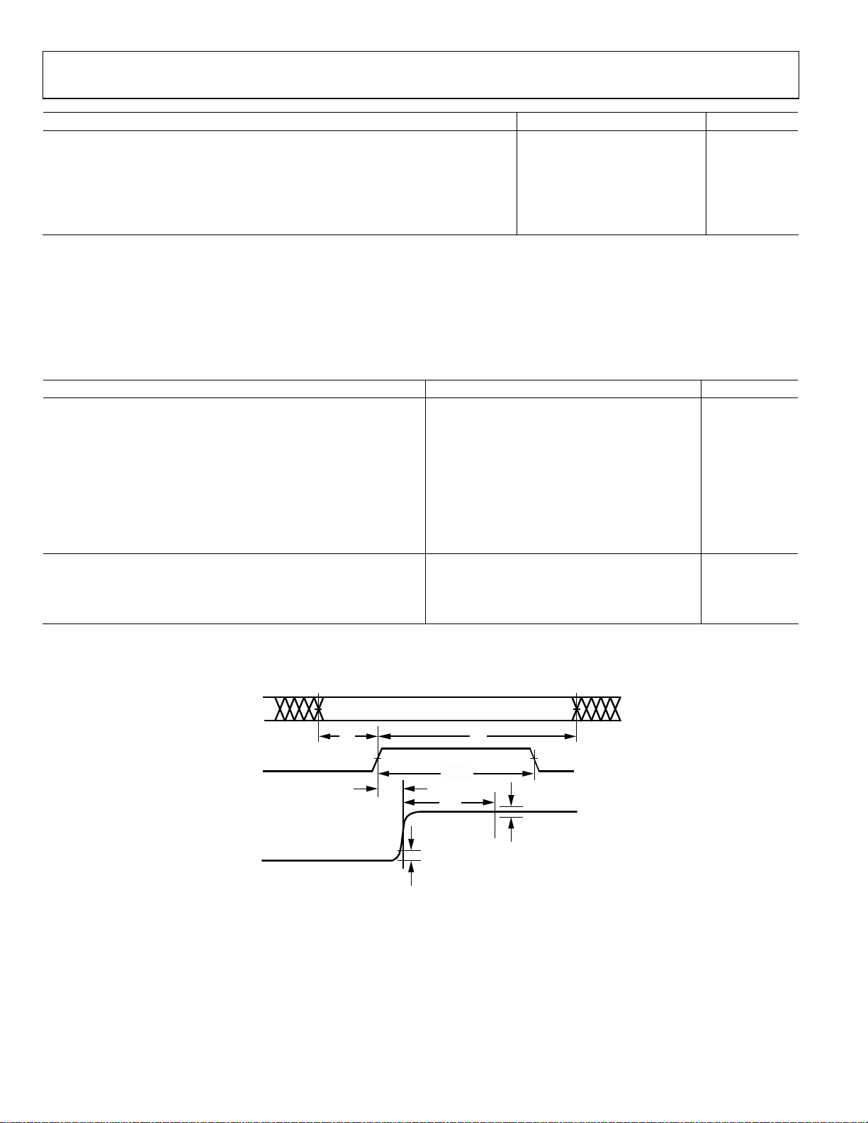
DB0–DB9
CLOCK
IOUTA
OR
IOUTB
t
S
t
PD
0.1%
t
t
ST
LPW
t
H
0.1%
02911-002
Figure 2. Timing Diagram
Rev. B | Page 6 of 32
AD9740
ABSOLUTE MAXIMUM RATINGS
Table 4.
With
Parameter
AVDD ACOM −0.3 +3.9 V
DVDD DCOM −0.3 +3.9 V
CLKVDD CLKCOM −0.3 +3.9 V
ACOM DCOM −0.3 +0.3 V
ACOM CLKCOM −0.3 +0.3 V
DCOM CLKCOM −0.3 +0.3 V
AVDD DVDD −3.9 +3.9 V
AVDD CLKVDD −3.9 +3.9 V
DVDD CLKVDD −3.9 +3.9 V
CLOCK, SLEEP DCOM −0.3 DVDD + 0.3 V
Digital Inputs, MODE DCOM −0.3 DVDD + 0.3 V
IOUTA, IOUTB ACOM −1.0 AVDD + 0.3 V
REFIO, REFLO, FS ADJ ACOM −0.3 AVDD + 0.3 V
CLK+, CLK−, MODE CLKCOM −0.3 CLKVDD + 0.3 V
Junction
Temperature
Storage
Temperature
Range
Lead Temperature
(10 sec)
Respect to
150 °C
−65 +150 °C
300 °C
Min Max Unit
Stresses above those listed under Absolute Maximum Ratings
may cause permanent damage to the device. This is a stress
rating only; functional operation of the device at these or any
other conditions above those indicated in the operational
sections of this specification is not implied. Exposure to
absolute maximum ratings for extended periods may effect
device reliability.
THERMAL CHARACTERISTICS
Thermal Resistance
28-Lead 300-Mil SOIC
= 55.9°C/W
θ
JA
28-Lead TSSOP
= 67.7°C/W
θ
JA
32-Lead LFCSP
= 32.5°C/W
θ
JA
1
Thermal impedance measurements were taken on a 4-layer board in still air,
in accordance with EIA/JESD51-7.
1
ESD CAUTION
ESD (electrostatic discharge) sensitive device. Electrostatic charges as high as 4000 V readily accumulate on
the human body and test equipment and can discharge without detection. Although this product features
proprietary ESD protection circuitry, permanent damage may occur on devices subjected to high energy
electrostatic discharges. Therefore, proper ESD precautions are recommended to avoid performance
degradation or loss of functionality.
Rev. B | Page 7 of 32

AD9740
(
PIN CONFIGURATIONS AND FUNCTION DESCRIPTIONS
MSB) DB9
1
2
DB8
3
DB7
4
DB6
5
DB5
6
DB4
DB3
DB2
DB1
DB0
NC
NC
NC REFLO
NC
AD9740
7
TOP VIEW
(Not to Scale)
8
9
10
11
12
13
14
NC = NO CONNECT
Figure 3. 28-Lead SOIC and TSSOP Pin Configuration
28
CLOCK
27
DVDD
26
DCOM
25
MODE
24
AVDD
23
RESERVED
22
IOUTA
21
IOUTB
20
ACOM
19
NC
18
FS ADJ
17
REFIO
16
15
SLEEP
02911-003
DB8
DB9 (MSB)
DB6
DB7
DCOM
DB4
DB5
1
2
29
3
30
3
1DB3
2DB2
3DVDD
4DB1
5DB0
6NC
7NC
8NC
PIN 1
INDICATOR
AD9740
TOP VIEW
(Not to Scale)
9
11
12
10
NC
CLK+
DCOM
CLKVDD
NC = NO CONNECT
SLEEP
26
25
28
27
24 FS ADJ
23 REFIO
22 ACOM
21 IOUTA
20 IOUTB
19 ACOM
18 AVDD
17 AVDD
13
14
15
16
–
CLK
MODE
CMODE
CLKCOM
02911-004
Figure 4. 32-Lead LFCSP Pin Configuration
Table 5. Pin Function Descriptions
SOIC/TSSOP
Pin No.
LFCSP
Pin No.
Mnemonic Description
1 27 DB9 (MSB) Most Significant Data Bit (MSB).
2 to 9 28 to 32, 1, 2, 4 DB8 to DB1 Data Bits 8 to 1.
10 5 DB0 (LSB) Least Significant Data Bit (LSB).
11 to 14, 19 6 to 9 NC No Internal Connection.
15 25 SLEEP
Power-Down Control Input. Active high. Contains active pull-down circuit; it can be
left unterminated if not used.
16 N/A REFLO
Reference Ground when Internal 1.2 V Reference Used. Connect to ACOM for both
internal and external reference operation modes.
17 23 REFIO
Reference Input/Output. Serves as reference input when using external reference.
Serves as 1.2 V reference output when using internal reference. Requires 0.1 μF capacitor
to ACOM when using internal reference.
18 24 FS ADJ Full-Scale Current Output Adjust.
20 19, 22 ACOM Analog Common.
21 20 IOUTB Complementary DAC Current Output. Full-scale current when all data bits are 0s.
22 21 IOUTA DAC Current Output. Full-scale current when all data bits are 1s.
23 N/A RESERVED Reserved. Do Not Connect to Common or Supply.
24 17, 18 AVDD Analog Supply Voltage (3.3 V).
25 16 MODE Selects Input Data Format. Connect to DCOM for straight binary, DVDD for twos complement.
N/A 15 CMODE
Clock Mode Selection. Connect to CLKCOM for single-ended clock receiver (drive CLK+
and float CLK–). Connect to CLKVDD for differential receiver. Float for PECL receiver
(terminations on-chip).
26 10, 26 DCOM Digital Common.
27 3 DVDD Digital Supply Voltage (3.3 V).
28 N/A CLOCK Clock Input. Data latched on positive edge of clock.
N/A 12 CLK+ Differential Clock Input.
N/A 13 CLK− Differential Clock Input.
N/A 11 CLKVDD Clock Supply Voltage (3.3 V).
N/A 14 CLKCOM Clock Common.
Rev. B | Page 8 of 32
AD9740
TERMINOLOGY
Linearity Error (Also Called Integral Nonlinearity or INL)
Linearity error is defined as the maximum deviation of the
actual analog output from the ideal output, determined by a
straight line drawn from zero to full scale.
Power Supply Rejection
The maximum change in the full-scale output as the supplies
are varied from nominal to minimum and maximum specified
voltages.
Differential Nonlinearity (or DNL)
DNL is the measure of the variation in analog value, normalized
to full scale, associated with a 1 LSB change in digital input code.
Monotonicity
A DAC is monotonic if the output either increases or remains
constant as the digital input increases.
Offset Error
The deviation of the output current from the ideal of zero is
called the offset error. For IOUTA, 0 mA output is expected
when the inputs are all 0s. For IOUTB, 0 mA output is expected
when all inputs are set to 1s.
Gain Error
The difference between the actual and ideal output span. The
actual span is determined by the output when all inputs are set
to 1s minus the output when all inputs are set to 0s.
Output Compliance Range
The range of allowable voltage at the output of a current output
DAC. Operation beyond the maximum compliance limits can
cause either output stage saturation or breakdown, resulting in
nonlinear performance.
Tem p er at u re Dr i ft
Temperature drift is specified as the maximum change from the
ambient (25°C) value to the value at either T
MIN
or T
MAX
. For
offset and gain drift, the drift is reported in ppm of full-scale
range (FSR) per °C. For reference drift, the drift is reported in
ppm per °C.
3.3V
Settling Time
The time required for the output to reach and remain within a
specified error band about its final value, measured from the
start of the output transition.
Glitch Impulse
Asymmetrical switching times in a DAC give rise to undesired
output transients that are quantified by a glitch impulse. It is
specified as the net area of the glitch in pV-s.
Spurious-Free Dynamic Range
The difference, in dB, between the rms amplitude of the output
signal and the peak spurious signal over the specified bandwidth.
Total Harmonic Distortion (THD)
T
THD is the ratio of the rms sum of the first six harmonic
components to the rms value of the measured input signal. It is
expressed as a percentage or in decibels (dB).
Multitone Power Ratio
The spurious-free dynamic range containing multiple carrier
tones of equal amplitude. It is measured as the difference
between the rms amplitude of a carrier tone to the peak
spurious signal in the region of a removed tone.
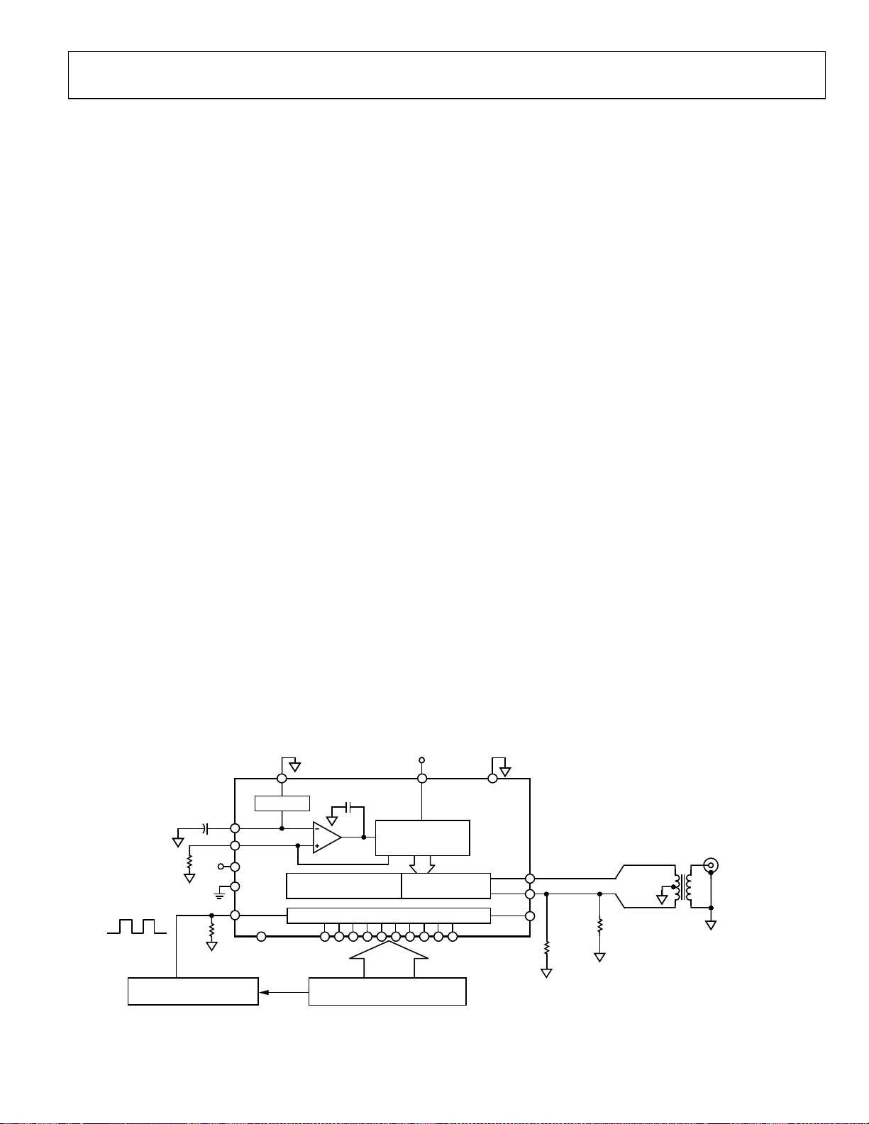
DVDD
DCOM
R
SET
2kΩ
50Ω
RETIMED
CLOCK
OUTPUT*
LECROY 9210
PULSE GENERATOR
0.1μF
3.3V
REFIO
FS ADJ
DVDD
DCOM
CLOCK
SLEEP
REFLO
1.2V REF
SEGMENTED SWITCHES
FOR DB9–DB1
CLOCK
OUTPUT
150pF
CURRENT SOURCE
LATCHES
DIGITAL
DATA
TEKTRONIX AWG-2021
WITH OPTION 4
AVDD ACOM
PMOS
ARRAY
LSB
SWITCHES
AD9740
IOUTA
IOUTB
MODE
50Ω
Figure 5. Basic AC Characterization Test Setup (SOIC/TSSOP Packages)
Rev. B | Page 9 of 32
MINI-CIRCUITS
T1-1T
50Ω
*AWG2021 CLOCK RETIMED
SO THAT THE DIGITAL DATA
TRANSITIONS ON FALLING EDGE
OF 50% DUTY CYCLE CLOCK.
ROHDE & SCHWARZ
FSEA30
SPECTRUM
ANALYZER
02911-005
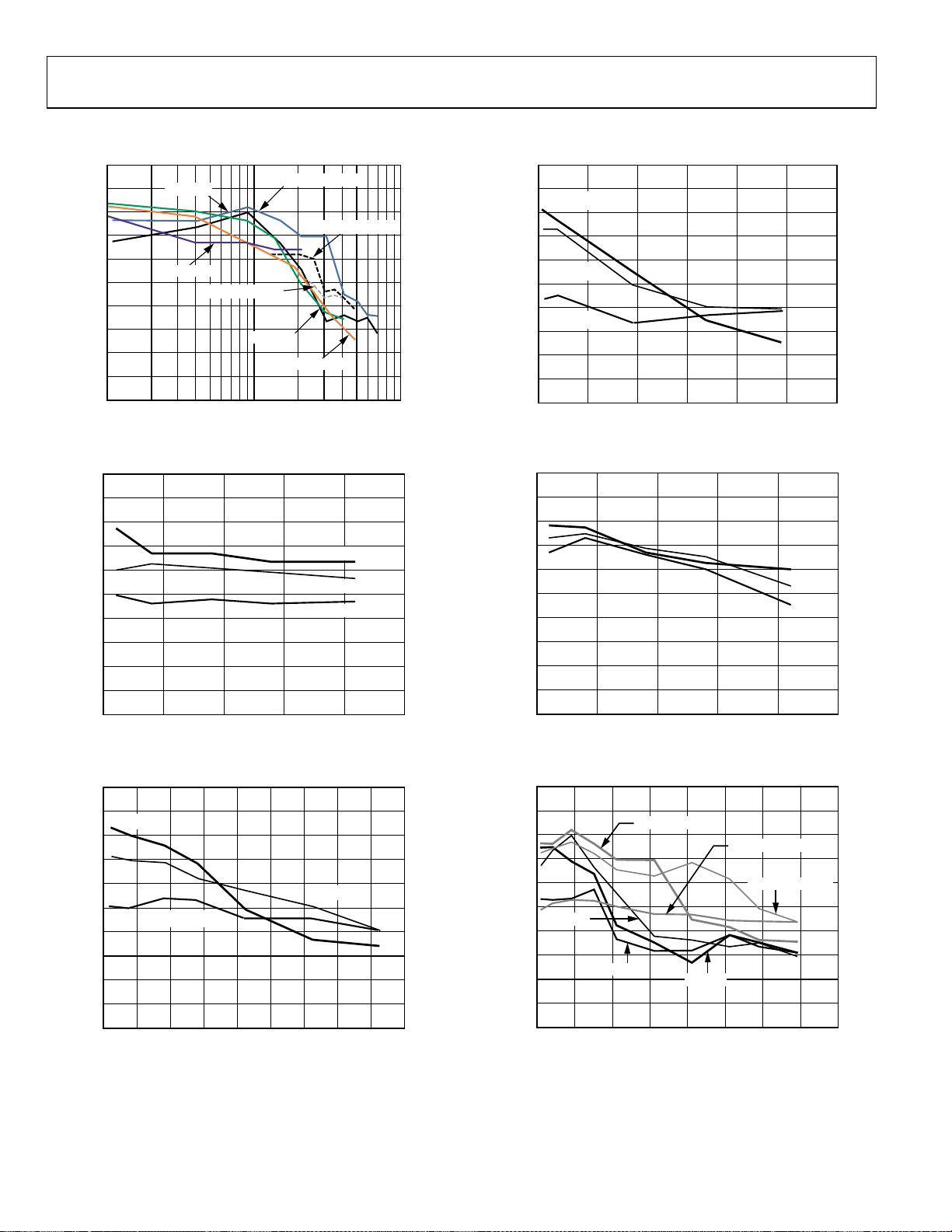
AD9740
TYPICAL PERFORMANCE CHARACTERISTICS
95
90
85
80
75
70
SFDR (dBc)
65
60
55
50
45
0 10 100
125MSPS
65MSPS
125MSPS (LFCSP)
f
Figure 6. SFDR vs. f
95
90
85
80
75
70
SFDR (dBc)
65
60
55
50
45
0 5 10 15 20 25
f
Figure 7. SFDR vs. f
95
90
0dBFS
85
80
75
70
SFDR (dBc)
65
60
55
50
45
01052015 3025 4035 45
–12dBFS
f
Figure 8. SFDR vs. f
OUT
OUT
OUT
210MSPS
(MHz)
(MHz)
OUT
(MHz)
OUT
210MSPS (LFCSP)
165MSPS (LFCSP)
165MSPS
@ 0 dBFS
OUT
@ 65 MSPS
@ 125 MSPS
–6dBFS
–12dBFS
–6dBFS
0dBFS
02911-006
02911-007
02911-008
95
90
85
80
75
70
SFDR (dBc)
65
60
55
50
45
95
90
85
80
75
70
SFDR (dBc)
65
60
55
50
45
95
90
85
80
75
70
SFDR (dBc)
65
60
55
50
45
0dBFS
–6dBFS
–12dBFS
02010 30 40 50 60
Figure 9. SFDR vs. f
01051520
Figure 10. SFDR vs. f
0dBFS
–12dBFS
02010 30 40 50 60 70 80
Figure 11. SFDR vs. f
f
(MHz)
OUT
OUT
f
(MHz)
OUT
and I
OUT
OUTFS
0dBFS (LFCSP)
–6dBFS
f
(MHz)
OUT
OUT
@ 165 MSPS
20mA
10mA
5mA
@ 65 MSPS and 0 dBFS
–12dBFS (LFCSP)
–6dBFS (LFCSP)
@ 210 MSPS
02911-009
25
02911-010
02911-054
Rev. B | Page 10 of 32
 Loading...