14-Bit, 2.5 GSPS,
SCLK
FEATURES
Direct RF synthesis at 2.5 GSPS update rate
DC to 1.25 GHz in baseband mode
1.25 GHz to 3.0 GHz in mix mode
Industry leading single/multicarrier IF or RF synthesis
Dual-port LVDS data interface
Up to 1.25 GSPS operation
Source synchronous DDR clocking
Pin-compatible with the AD9739
Programmable output current: 8.7 mA to 31.7 mA
Low power: 1.1 W at 2.5 GSPS
APPLICATIONS
Broadband communications systems
DOCSIS CMTS systems
Military jammers
Instrumentation, automatic test equipment
Radar, avionics
RF Digital-to-Analog Converter
AD9739A
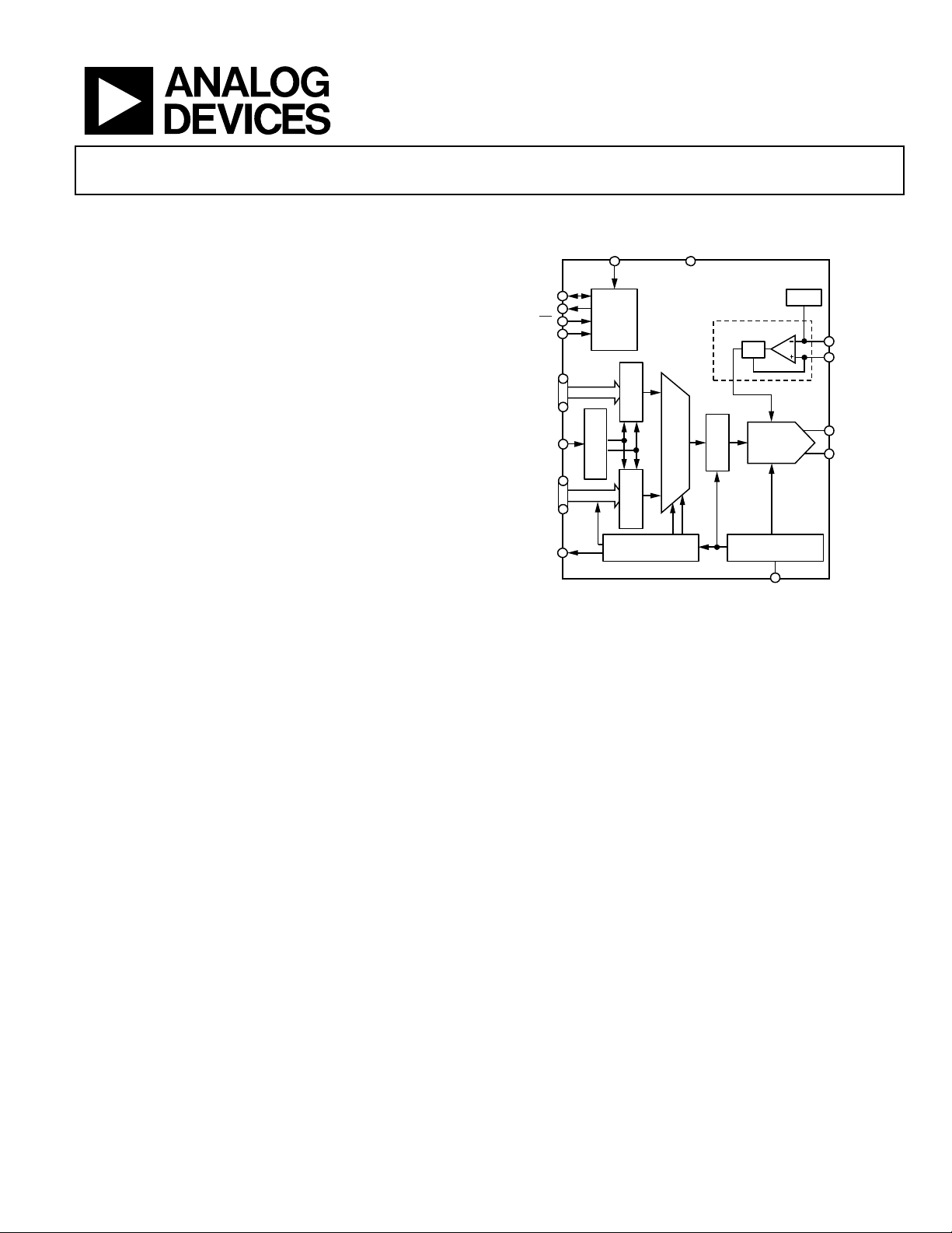
FUNCTIONAL BLOCK DIAGRAM
SDIO
SDO
CS
DCI
DCO
RESET
SPI
DB0[13:0]DB1[13:0]
LVDS DDR
DATA
CONTROLLER
LVDS DDR
(DIV-BY-4)
IRQ
AD9739A
1.2V
DAC BIAS
RECEIVER
TxDAC
DATA
4-TO-1
DATA ASSEMBLER
RECEIVER
CLK DISTRIBUTION
CORE
LATCH
DLL
(MU CONTROL LER)
VREF
I120
IOUTN
IOUTP
GENERAL DESCRIPTION
The AD9739A is a 14-bit, 2.5 GSPS high performance RF DAC
capable of synthesizing wideband signals from dc up to 3 GHz.
The AD9739A is pin and functionally compatible with the AD9739
with the exception that the AD9739A does not support
synchronization and is specified to operate between 1.6 GSPS
and 2.5 GSPS. By elimination of the synchronization circuitry,
some nonideal artifacts such as images and discrete clock spurs
remain stationary on the AD9739A between power-up cycles,
thus allowing for possible system calibration. AC linearity and
noise performance remain the same between the AD9739 and
AD9739A.
The inclusion of on-chip controllers simplifies system integration. A dual-port, source synchronous, LVDS interface
simplifies the digital interface with existing FGPA/ASIC
technology. On-chip controllers are used to manage external
and internal clock domain variations over temperature to
ensure reliable data transfer from the host to the DAC core. A
serial peripheral interface (SPI) is used for device configuration
as well as readback of status registers.
The AD9739A is manufactured on a 0.18 μm CMOS process
and operates from 1.8 V and 3.3 V supplies. It is supplied in a
160-ball chip scale ball grid array for reduced package parasitics.
Rev. A
Information furnished by Analog Devices is believed to be accurate and reliable. However, no
responsibility is assumed by Analog Devices for its use, nor for any infringements of patents or other
rights of third parties that may result from its use. Specifications subject to change without notice. No
license is granted by implication or otherwise under any patent or patent rights of Analog Devices.
Trademarks and registered trademarks are the property of their respective owners.
DACCLK
Figure 1.
PRODUCT HIGHLIGHTS
1. Ability to synthesize high quality wideband signals with
bandwidths of up to 1.25 GHz in the first or second
Nyquist zone.
2. A proprietary quad-switch DAC architecture provides
exceptional ac linearity performance while enabling mixmode operation.
3. A dual-port, double data rate, LVDS interface supports the
maximum conversion rate of 2500 MSPS.
4. On-chip controllers manage external and internal clock
domain skews.
5. Programmable differential current output with a 8.66 mA
to 31.66 mA range.
One Technology Way, P.O. Box 9106, Norwood, MA 02062-9106, U.S.A.
Tel: 781.329.4700 www.analog.com
Fax: 781.461.3113 ©2011 Analog Devices, Inc. All rights reserved.
09616-001

AD9739A
TABLE OF CONTENTS
Features .............................................................................................. 1
Applications ....................................................................................... 1
Functional Block Diagram .............................................................. 1
General Description ......................................................................... 1
Product Highlights ........................................................................... 1
Revision History ............................................................................... 2
Specifications ..................................................................................... 3
DC Specifications ......................................................................... 3
LVDS Digital Specifications ........................................................ 4
Serial Port Specifications ............................................................. 5
AC Specifications .......................................................................... 6
Absolute Maximum Ratings ............................................................ 7
Thermal Resistance ...................................................................... 7
ESD Caution .................................................................................. 7
Pin Configurations and Function Descriptions ........................... 8
Typical Performance Characteristics ........................................... 11
AC (Normal Mode) .................................................................... 11
AC (Mix Mode) .......................................................................... 14
One-Carrier DOCSIS Performance (Normal Mode) ............ 16
Four-Carrier DOCSIS Performance (Normal Mode) ........... 17
Eight-Carrier DOCSIS Performance (Normal Mode) .......... 18
16-Carrier DOCSIS Performance (Normal Mode) ............... 19
32-Carrier DOCSIS Performance (Normal Mode) ............... 20
64- and 128-Carrier DOCSIS Performance (Normal Mode)21
Terminolog y .................................................................................... 22
Serial Port Interface (SPI) Register .............................................. 23
SPI Register Map Description .................................................. 23
SPI Operation ............................................................................. 23
SPI Register Map ........................................................................ 25
Theory of Operation ...................................................................... 28
LVDS Data Port Interface .......................................................... 29
Mu Controller ............................................................................. 32
Interrupt Requests ...................................................................... 33
Analog Interface Considerations .................................................. 35
Analog Modes of Operation ..................................................... 35
Clock Input Considerations ...................................................... 36
Voltage Reference ....................................................................... 37
Analog Outputs .......................................................................... 37
Nonideal Spectral Artifacts ....................................................... 39
Lab Evaluation of the AD9739A .............................................. 40
Recommended Start-Up Sequence .......................................... 41
Outline Dimensions ....................................................................... 43
Ordering Guide .......................................................................... 43
REVISION HISTORY
7/11—Rev 0 to Rev. A
Changed Maximum Update Rate (DACCLK Input) Parameter
to DAC Clock Rate Parameter in Table 4 ...................................... 6
Added Adjusted DAC Update Rate Parameter and Endnote 1 in
Table 4 ................................................................................................ 6
Updated Outline Dimensions ....................................................... 43
1/11—Revision 0: Initial Version
Rev. A | Page 2 of 44

AD9739A
SPECIFICATIONS
DC SPECIFICATIONS
VDDA = VDD33 = 3.3 V ± 6%, VDDC = VDD = 1.8 V ± 6%, I
Table 1.
Parameter Min Typ Max Unit
RESOLUTION 14 Bits
ACCURACY
Integral Nonlinearity (INL) ±2.5 LSB
Differential Nonlinearity (DNL) ±2.0 LSB
ANALOG OUTPUTS
Gain Error (with Internal Reference) 5.5 %
Full-Scale Output Current 8.66 20.2 31.66 mA
Output Compliance Range −1.0 +1.0 V
Common-Mode Output Resistance 10 MΩ
Differential Output Resistance 70 Ω
Output Capacitance 1 pF
DAC CLOCK INPUT (DACCLK_P, DACCLK_N)
Differential Peak-to-Peak Voltage 1.2 1.6 2.0 V
Common-Mode Voltage 900 mV
Clock Rate 1.6 2.5 GHz
TEMPERATURE DRIFT
Gain 60 ppm/°C
Reference Voltage 20 ppm/°C
REFERENCE
Internal Reference Voltage 1.15 1.2 1.25 V
Output Resistance 5 kΩ
ANALOG SUPPLY VOLTAGES
VDDA 3.1 3.3 3.5 V
VDDC 1.70 1.8 1.90 V
DIGITAL SUPPLY VOLTAGES
VDD33 3.10 3.3 3.5 V
VDD 1.70 1.8 1.90 V
SUPPLY CURRENTS AND POWER DISSIPATION, 2.0 GSPS
I
37 38 mA
VDDA
I
158 167 mA
VDDC
I
14.5 16 mA
VDD33
I
173 183 mA
VDD
Power Dissipation 0.770 W
Sleep Mode, I
2.5 2.75 mA
VDDA
Power-Down Mode (All Power-Down Bits Set in Register 0x01 and
Register 0x02)
I
0.02 mA
VDDA
I
6 mA
VDDC
I
0.6 mA
VDD33
I
0.1 mA
VDD
SUPPLY CURRENTS AND POWER DISSIPATION, 2.5 GSPS
I
37 mA
VDDA
I
223 mA
VDDC
I
14.5 mA
VDD33
I
215 mA
VDD
Power Dissipation 0.960 W
OUTFS
= 20 mA.
Rev. A | Page 3 of 44

AD9739A
LVDS DIGITAL SPECIFICATIONS
VDDA = VDD33 = 3.3 V ± 6%, VDDC = VDD = 1.8 V ± 6%, I
Standard 1596.3-1996 reduced range link, unless otherwise noted.
Table 2.
Parameter Min Typ Max Unit
LVDS DATA INPUTS (DB0[13:0], DB1[13:0])1
Input Common-Mode Voltage Range, V
Logic High Differential Input Threshold, V
Logic Low Differential Input Threshold, V
825 1575 mV
COM
175 400 mV
IH_DTH
−175 −400 mV
IL_DTH
Receiver Differential Input Impedance, RIN 80 120 Ω
Input Capacitance 1.2 pF
LVDS Input Rate 1250 MSPS
LVDS Minimum Data Valid Period (t
) (See Figure 76) 344 ps
MDE
LVDS CLOCK INPUT (DCI)2
Input Common-Mode Voltage Range, V
Logic High Differential Input Threshold, V
Logic Low Differential Input Threshold, V
825 1575 mV
COM
175 400 mV
IH_DTH
−175 −400 mV
IL_DTH
Receiver Differential Input Impedance, RIN 80 120 Ω
Input Capacitance 1.2 pF
Maximum Clock Rate 625 MHz
LVDS CLOCK OUTPUT (DCO)3
Output Voltage High (DCO_P or DCO_N) 1375 mV
Output Voltage Low (DCO_P or DCO_N) 1025 mV
Output Differential Voltage, |VOD| 150 200 250 mV
Output Offset Voltage, VOS 1150 1250 mV
Output Impedance, Single-Ended, RO 80 100 120 Ω
RO Single-Ended Mismatch 10 %
Maximum Clock Rate 625 MHz
1
DB0[x]P, DB0[x]N, DB1[x]P, and DB1[x]N pins.
2
DCI_P and DCI_N pins.
3
DCO_P and DCO_N pins with 100 Ω differential termination.
= 20 mA. LVDS drivers and receivers are compliant to the IEEE
OUTFS
Rev. A | Page 4 of 44

AD9739A
SERIAL PORT SPECIFICATIONS
VDDA = VDD33 = 3.3 V ± 6%, VDDC = VDD = 1.8 V ± 6%.
Tabl e 3
.
Parameter Min Typ Max Unit
WRITE OPERATION (See Figure 71)
SCLK Clock Rate, f
SCLK Clock High, tHI 18 ns
SCLK Clock Low, t
SDIO to SCLK Setup Time, tDS 2 ns
SCLK to SDIO Hold Time, tDH 1 ns
CS to SCLK Setup Time, tS
SCLK to CS Hold Time, tH
READ OPERATION (See Figure 72 and Figure 73)
SCLK Clock Rate, f
SCLK Clock High, tHI 18 ns
SCLK Clock Low, t
SDIO to SCLK Setup Time, tDS 2 ns
SCLK to SDIO Hold Time, tDH 1 ns
CS to SCLK Setup Time, tS
SCLK to SDIO (or SDO) Data Valid Time, tDV 15 ns
CS to SDIO (or SDO) Output Valid to High-Z, tEZ
INPUTS (SDI, SDIO, SCLK, CS)
Voltage in High, VIH 2.0 3.3 V
Voltage in Low, VIL 0 0.8 V
Current in High, IIH −10 +10 μA
Current in Low, IIL −10 +10 μA
OUTPUT (SDIO)
Voltage Out High, VOH 2.4 3.5 V
Voltage Out Low, VOL 0 0.4 V
Current Out High, IOH 4 mA
Current Out Low, IOL 4 mA
, 1/t
SCLK
LOW
20 MHz
SCLK
18 ns
3 ns
2 ns
, 1/t
SCLK
LOW
20 MHz
SCLK
18 ns
3 ns
2 ns
Rev. A | Page 5 of 44

AD9739A
AC SPECIFICATIONS
VDDA = VDD33 = 3.3 V ± 6%, VDDC = VDD = 1.8 V ± 6%, I
Table 4.
Parameter Min Typ Max Unit
DYNAMIC PERFORMANCE
DAC Clock Rate 800 2500 MSPS
Adjusted DAC Update Rate1 800 2500 MSPS
Output Settling Time to 0.1% 13 ns
SPURIOUS-FREE DYNAMIC RANGE (SFDR)
f
= 100 MHz 69.5 dBc
OUT
f
= 350 MHz 58.5 dBc
OUT
f
= 550 MHz 54 dBc
OUT
f
= 950 MHz 60 dBc
OUT
TWO-TONE INTERMODULATION DISTORTION (IMD), f
f
= 100 MHz 94 dBc
OUT
f
= 350 MHz 78 dBc
OUT
f
= 550 MHz 72 dBc
OUT
f
= 950 MHz 68 dBc
OUT
OUT2
= f
OUT1
NOISE SPECTRAL DENSITY (NSD), 0 dBFS SINGLE TONE
f
= 100 MHz −166 dBm/Hz
OUT
f
= 350 MHz −161 dBm/Hz
OUT
f
= 550 MHz −160 dBm/Hz
OUT
f
= 850 MHz −160 dBm/Hz
OUT
WCDMA ACLR (SINGLE CARRIER), ADJACENT/ALTERNATE ADJACENT CHANNEL
f
= 2457.6 MSPS f
DAC
f
= 2457.6 MSPS, f
DAC
f
= 2457.6 MSPS, f
DAC
f
= 2457.6 MSPS, f
DAC
1
Adjusted DAC updated rate is calculated as f
with f
= 2500 MSPS, f
DAC
= 350 MHz 80/80 dBc
OUT
= 950 MHz 78/79 dBc
OUT
= 1700 MHz (Mix Mode) 74/74 dBc
OUT
= 2100 MHz (Mix Mode) 69/72 dBc
OUT
divided by the minimum required interpolation factor. For the AD9739A, the minimum interpolation factor is 1. Thus,
, adjusted, = 2500 MSPS.
DAC
DAC
= 20 mA.
OUTFS
+ 1.25 MHz
Rev. A | Page 6 of 44
AD9739A
ABSOLUTE MAXIMUM RATINGS
Table 5.
With
Parameter
VDDA VSSA −0.3 V to +3.6 V
VDD33 VSS −0.3 V to +3.6 V
VDD VSS −0.3 V to +1.98 V
VDDC VSSC −0.3 V to +1.98 V
VSSA VSS −0.3 V to +0.3 V
VSSA VSSC −0.3 V to +0.3 V
VSS VSSC −0.3 V to +0.3 V
DACCLK_P,
DACCLK_N
DCI, DCO VSS −0.3 V to VDD33 + 0.3 V
LVDS Data Inputs VSS −0.3 V to VDD33 + 0.3 V
IOUTP, IOUTN VSSA −1.0 V to VDDA + 0.3 V
I120, VREF VSSA −0.3 V to VDDA + 0.3 V
IRQ, CS, SCLK, SDO,
SDIO, RESET
Junction
Temperature
Storage Temperature −65°C to +150°C
Respect To
VSSC −0.3 V to VDDC + 0.18 V
VSS −0.3 V to VDD33 + 0.3 V
150°C
Rating
Stresses above those listed under Absolute Maximum Ratings
may cause permanent damage to the device. This is a stress
rating only; functional operation of the device at these or any
other conditions above those indicated in the operational
section of this specification is not implied. Exposure to absolute
maximum rating conditions for extended periods may affect
device reliability.
THERMAL RESISTANCE
θJA is specified for the worst-case conditions, that is, a device
soldered in a circuit board for surface-mount packages.
Table 6. Thermal Resistance
Package Type θJA θ
160-Ball CSP_BGA 31.2 7.0 °C/W1
1
With no airflow movement.
Unit
JC
ESD CAUTION
Rev. A | Page 7 of 44
AD9739A
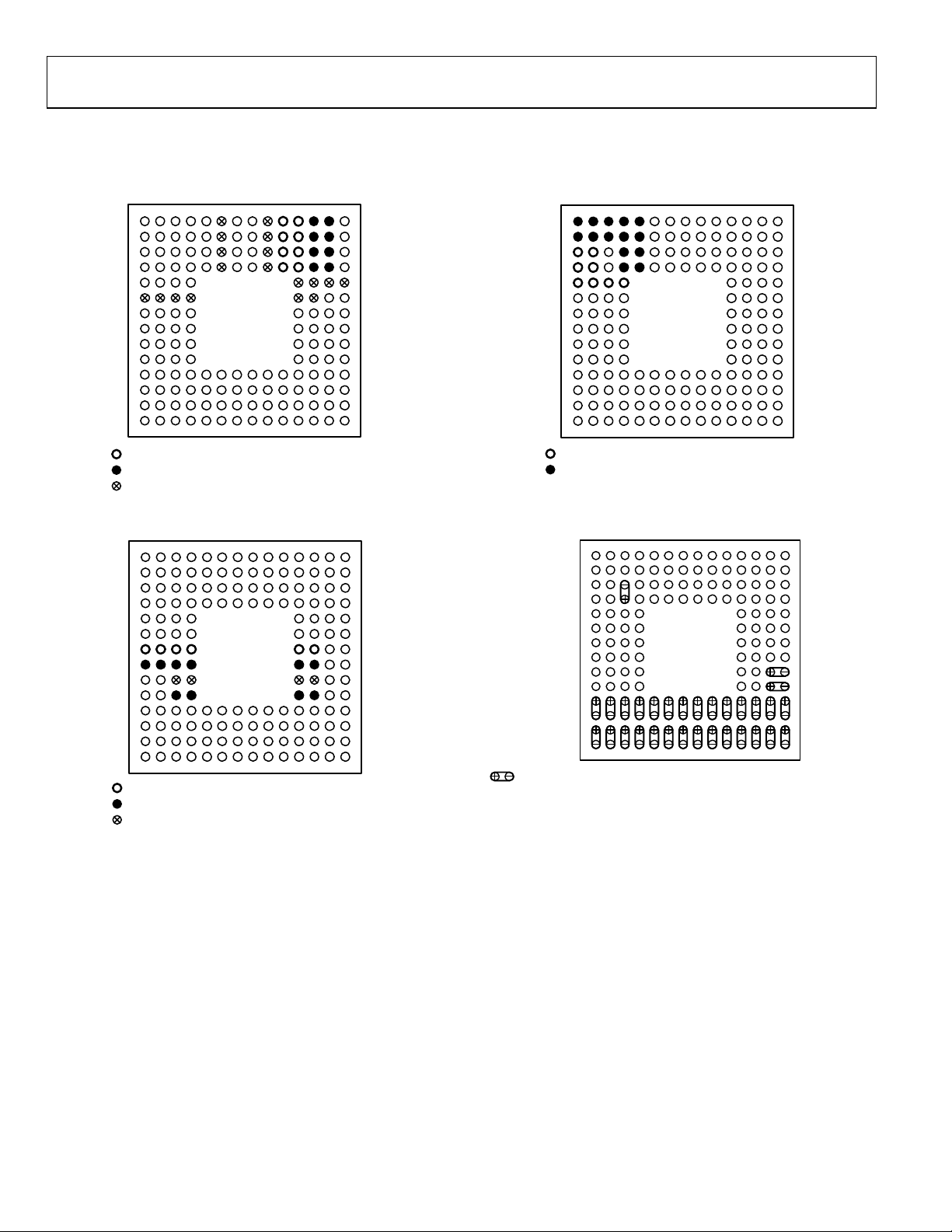
PIN CONFIGURATIONS AND FUNCTION DESCRIPTIONS
1413121110876321954
1413121110876321954
A
B
C
D
E
F
G
H
J
K
L
M
N
P
VDDA, 3.3V, ANALOG SUPPLY
VSSA, ANALOG SUPPLY GROUND
VSSA SHIELD, ANALOG SUPPLY GROUND SHIELD
Figure 2. Analog Supply Pins (Top View)
A
B
C
D
E
F
G
H
J
K
L
M
N
P
VDD, 1.8V, DIGITAL SUPPLY
VSS DIGITAL SUPPLY GROUND
VDD33, 3.3V DI GITAL SUPPLY
Figure 3. Digital Supply Pins (Top View)
A
B
C
D
E
F
G
H
J
K
L
M
N
P
VDDC, 1.8V, CLOCK SUPPLY
VSSC, CLOCK SUPPLY GROUND
09616-002
09616-004
Figure 4. Digital LVDS Clock Supply Pins (Top View)
1413121110876321954
A
B
DACCLK_N
DACCLK_P
DB1[0:13] P
DB1[0:13]N
DB0[0:13] P
DB0[0:13]N
09616-003
C
D
E
F
G
H
J
K
L
M
N
P
DIFFERE NTIAL INPUT SIGNAL (CL OCK OR DATA)
1413121110876321954
DCO_P/_N
DCI_P/_N
09616-005
Figure 5. Digital LVDS Input, Clock I/O (Top View)
Rev. A | Page 8 of 44
AD9739A
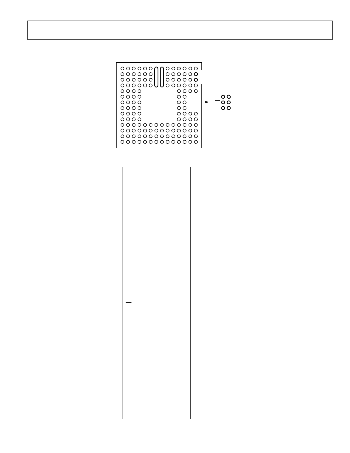
IOUTN
IOUTP
1413121110876321954
A
B
C
D
E
F
G
H
J
K
L
M
N
P
Figure 6. Analog I/O and SPI Control Pins (Top View)
I120
VREF
IRQ
CS
SCLK
RESET
SDIO
SDO
09616-006
Table 7. AD9739A Pin Function Descriptions
Pin No. Mnemonic Description
C1, C2, D1, D2, E1, E2, E3, E4 VDDC 1.8 V Clock Supply Input.
A1, A2, A3, A4, A5, B1, B2, B3, B4, B5, C4,
VSSC
Clock Supply Return.
C5, D4, D5
A10, A11, B10, B11, C10, C11, D10, D11 VDDA
A12, A13, B12, B13, C12, C13, D12, D13, VSSA
A6, A9, B6, B9, C6, C9, D6, D9, F1, F2, F3,
VSSA Shield Analog Supply Return Shield.
F4, E11, E12, E13, E14, F11, F12
A14 NC
A7, B7, C7, D7 IOUTN
A8, B8, C8, D8 IOUTP
B14 I120
3.3 V Analog Supply Input.
Analog Supply Return.
Tie to VSSA at the DAC.
Do not connect to this pin.
DAC Negative Current Output Source.
DAC Positive Current Output Source.
Nominal 1.2 V Reference. Tie to analog ground via a 10 kΩ
resistor to generate a 120 μA reference current.
C14 VREF Voltage Reference Input/Output.
Decouple to VSSA with a 1 nF capacitor.
D14 NC
C3, D3 DACCLK_N/DACCLK_P
F13 IRQ
Factory Test Pin. Do not connect to this pin.
Negative/Positive DAC Clock Input (DACCLK).
Interrupt Request Open Drain Output. Active high. Pull up to
VDD33 with a 10 kΩ resistor.
F14 RESET
G13
CS
G14 SDIO
H13 SCLK
H14 SDO
J3, J4, J11, J12 VDD33
G1, G2, G3, G4, G11, G12 VDD
H1, H2, H3, H4, H11, H12, K3, K4, K11, K12 VSS
J1, J2 NC
Reset Input. Active high. Tie to VSS if unused.
Serial Port Enable Input.
Serial Port Data Input/Output.
Serial Port Clock Input.
Serial Port Data Output.
3.3 V Digital Supply Input.
1.8 V Digital Supply. Input.
Digital Supply Return.
Differential resistor of 200 Ω exists between J1 and J2. Do not
connect to this pin.
K1, K2 NC
Differential resistor of 100 Ω exists between J1 and J2. Do not
connect to this pin.
J13, J14 DCO_P/DCO_N
K13, K14 DCI_P/DCI_N
L1, M1 DB1[0]P/DB1[0]N
L2, M2 DB1[1]P/DB1[1]N
L3, M3 DB1[2]P/DB1[2]N
Positive/Negative Data Clock Output (DCO).
Positive/Negative Data Clock Input (DCI).
Port 1 Positive/Negative Data Input Bit 0.
Port 1 Positive/Negative Data Input Bit 1.
Port 1 Positive/Negative Data Input Bit 2.
L4, M4 DB1[3]P/DB1[3]N Port 1 Positive/Negative Data Input Bit 3.
Rev. A | Page 9 of 44

AD9739A
Pin No. Mnemonic Description
L5, M5 DB1[4]P/DB1[4]N Port 1 Positive/Negative Data Input Bit 4.
L6, M6 DB1[5]P/DB1[5]N Port 1 Positive/Negative Data Input Bit 5.
L7, M7 DB1[6]P/DB1[6]N Port 1 Positive/Negative Data Input Bit 6.
L8, M8 DB1[7]P/DB1[7]N Port 1 Positive/Negative Data Input Bit 7.
L9, M9 DB1[8]P/DB1[8]N Port 1 Positive/Negative Data Input Bit 8.
L10, M10 DB1[9]P/DB1[9]N Port 1 Positive/Negative Data Input Bit 9.
L11, M11 DB1[10]P/DB1[10]N Port 1 Positive/Negative Data Input Bit 10.
L12, M12 DB1[11]P/DB1[11]N Port 1 Positive/Negative Data Input Bit 11.
L13, M13 DB1[12]P/DB1[12]N Port 1 Positive/Negative Data Input Bit 12.
L14, M14 DB1[13]P/DB1[13]N Port 1 Positive/Negative Data Input Bit 13.
N1, P1 DB0[0]P/DB0[0]N Port 0 Positive/Negative Data Input Bit 0.
N2, P2 DB0[1]P/DB0[1]N Port 0 Positive/Negative Data Input Bit 1.
N3, P3 DB0[2]P/DB0[2]N Port 0 Positive/Negative Data Input Bit 2.
N4, P4 DB0[3]P/DB0[3]N Port 0 Positive/Negative Data Input Bit 3.
N5, P5 DB0[4]P/DB0[4]N Port 0 Positive/Negative Data Input Bit 4.
N6, P6 DB0[5]P/DB0[5]N Port 0 Positive/Negative Data Input Bit 5.
N7, P7 DB0[6]P/DB0[6]N Port 0 Positive/Negative Data Input Bit 6.
N8, P8 DB0[7]P/DB0[7]N Port 0 Positive/Negative Data Input Bit 7.
N9, P9 DB0[8]P/DB0[8]N Port 0 Positive/Negative Data Input Bit 8.
N10, P10 DB0[9]P/DB0[9]N Port 0 Positive/Negative Data Input Bit 9.
N11, P11 DB0[10]P/DB0[10]N Port 0 Positive/Negative Data Input Bit 10.
N12, P12 DB0[11]P/DB0[11]N Port 0 Positive/Negative Data Input Bit 11.
N13, P13 DB0[12]P/DB0[12]N Port 0 Positive/Negative Data Input Bit 12.
N14, P14 DB0[13]P/DB0[13]N Port 0 Positive/Negative Data Input Bit 13.
Rev. A | Page 10 of 44
AD9739A
–
–
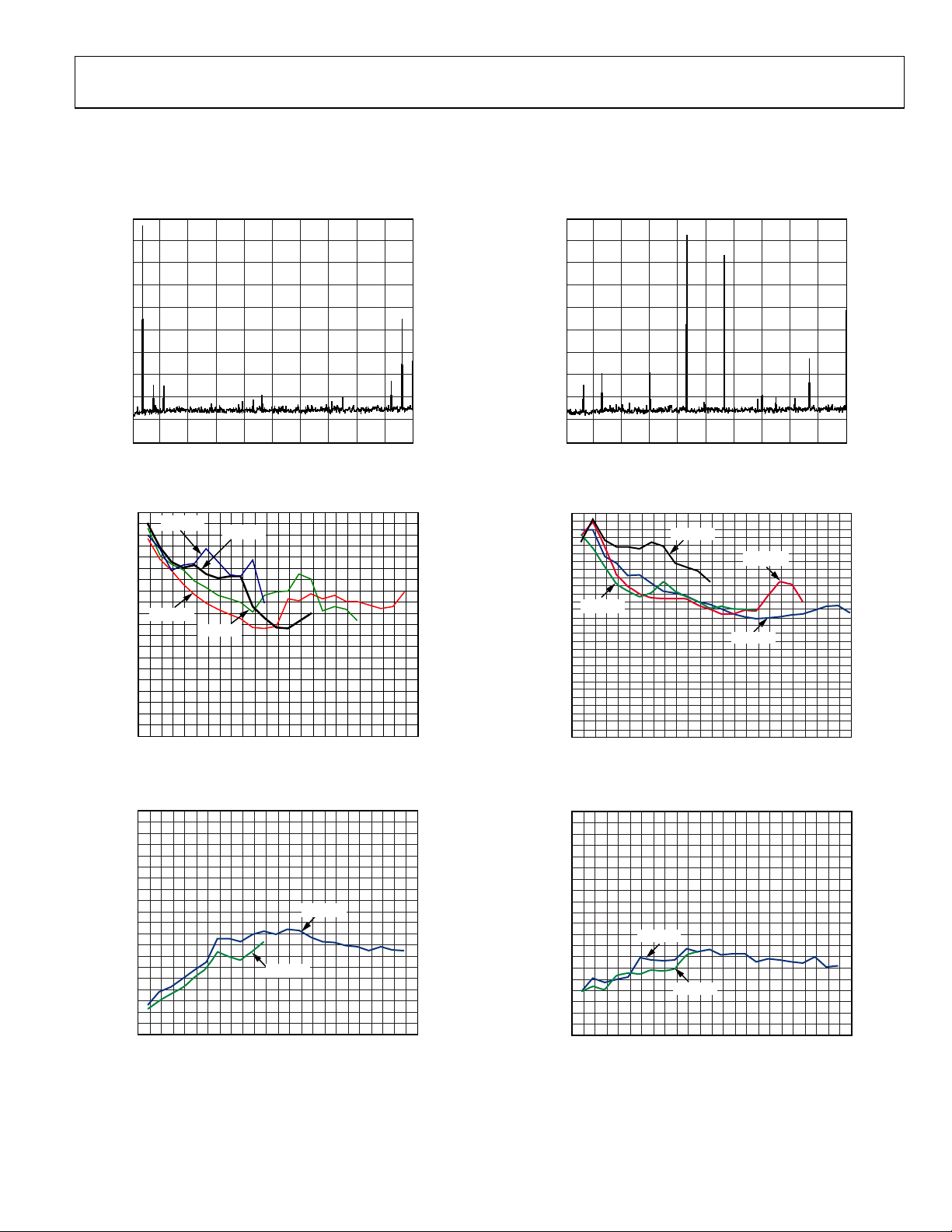
TYPICAL PERFORMANCE CHARACTERISTICS
AC (NORMAL MODE)
I
= 20 mA, nominal supplies, 25°C, unless otherwise noted.
OUTFS
10dB/DIV
Figure 7. Single-Tone Spectrum at f
80
1.2GSPS
75
70
65
60
2.4GSPS
55
50
SFDR (dBc)
45
40
35
30
0 100 200 300 400 500 600 700 800 900 1000 1100 1200
2.0GSPS
Figure 8. SFDR vs. f
150
–152
–154
–156
–158
–160
–162
NSD (dBm/Hz)
–164
–166
–168
–170
0 100 200 300 400 500 600 700 800 900 1000 110 0 1200
Figure 9. Single-Tone NSD over f
VBW 10kHz
1.6GSPS
f
f
OUT
OUT
OUT
(MHz)
OUT
1.2GSPS
(MHz)
= 91 MHz, f
over f
DAC
2.4GSPS
OUT
STOP 2.4GHzSTART 20MHz
DAC
= 2.4 GSPS
10dB/DIV
STOP 2.4GHzSTART 20MHz
2.4GSPS
VBW 10kHz
1.2GSPS
f
OUT
1.2GSPS
f
OUT
= 1091 MHz, f
OUT
2.4GSPS
(MHz)
over f
OUT
(MHz)
2.0GSPS
DAC
OUT
DAC
= 2.4 GSPS
1100 1200
09616-010
09616-011
09616-012
09616-007
Figure 10. Single-Tone Spectrum at f
100
95
90
85
80
75
1.6GSPS
70
65
60
IMD (dBc)
55
50
45
40
35
30
0 100 200 300 400 500 600 700 800 90 0 1000
09616-008
Figure 11. IMD vs. f
160
–161
–162
–163
–164
–165
–166
NSD (dBm/Hz)
–167
–168
–169
–170
0 100 200 300 400 500 600 700 800 900 1000 1100 1200
09616-009
Figure 12. Eight-Tone NSD over f
Rev. A | Page 11 of 44
AD9739A
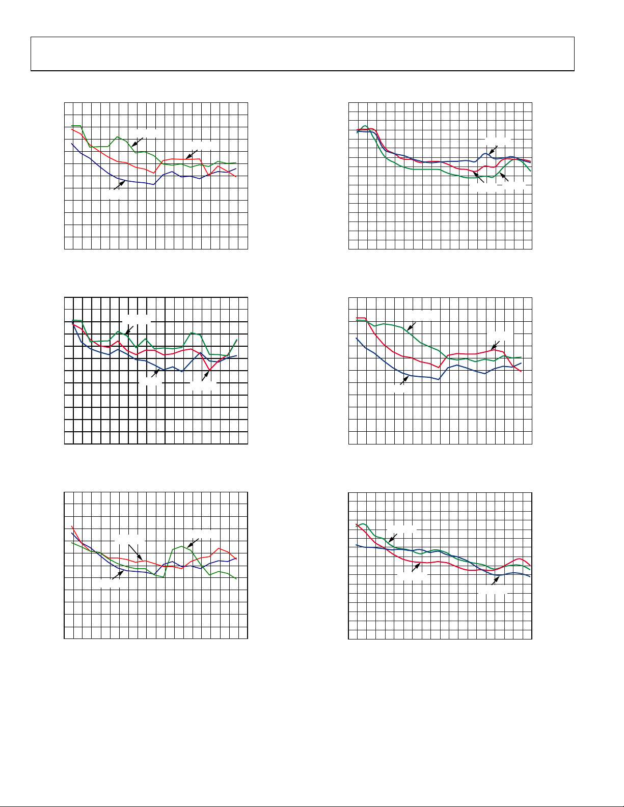
f
= 2 GSPS, I
DAC
90
= 20 mA, nominal supplies, 25°C, unless otherwise noted.
OUTFS
110
80
70
60
SFDR (dBc)
50
40
30
0 100 200 300 400 500 600 700 800 900 1000
Figure 13. SFDR vs. f
90
80
70
60
SFDR (dB)
50
0dBFS
–6dBFS
f
(MHz)
OUT
over Digital Full Scale
OUT
–6dBFS
0dBFS
–3dBFS
–3dBFS
100
90
80
70
IMD (dBc)
60
50
40
30
0 100 200 300 400 500 600 700 800 900 1000
f
(MHz)
09616-013
Figure 16. IMD vs. f
90
80
70
60
SFDR (dB)
50
0dBFS
OUT
over Digital Full Scale
OUT
–6dBFS
–3dBFS
–6dBFS
–3dBFS
0dBFS
09616-016
40
30
0 100 200 300 400 500 600 700 800 900 1000
f
(MHz)
OUT
Figure 14. SFDR for Second Harmonic over f
90
80
70
60
SFDR (dBc)
50
40
30
0 100 200 300 400 500 600 700 800 900 1000
10mA FS
20mA FS
f
OUT
Figure 15. SFDR vs. f
(MHz)
OUT
OUT
30mA FS
over DAC I
vs. Digital Full Scale
OUTFS
40
30
0 100 200 300 400 500 600 700 800 900 1000
f
(MHz)
10mA FS
f
OUT
OUT
(MHz)
over DAC I
OUT
vs. Digital Full Scale
OUT
30mA FS
OUTFS
09616-014
Figure 17. SFDR for Third Harmonic over f
110
100
90
80
70
IMD (dBc)
60
50
40
30
0 100 200 300 400 500 600 700 800 900 1000
09616-015
20mA FS
Figure 18. IMD vs. f
9616-017
09616-018
Rev. A | Page 12 of 44
AD9739A
–
–
–
90
110
80
70
–40°C
+85°C
60
SFDR (dBc)
50
+25°C
40
30
0 100 200 300 400 500 600 700 800 900 1000
f
(MHz)
OUT
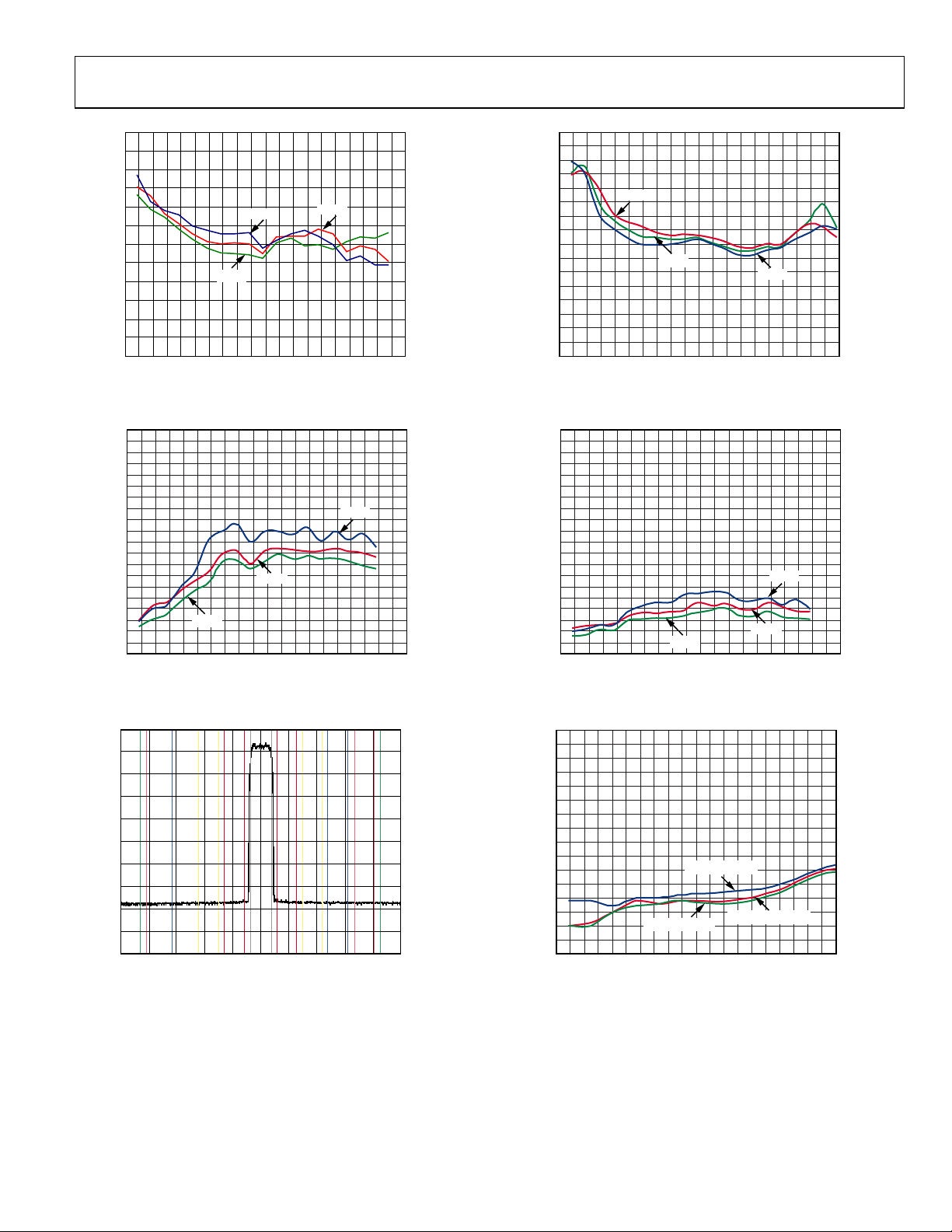
Figure 19. SFDR vs. f
over Temperature
OUT
150
–152
–154
–156
–158
–40°C
–160
–162
NSD (dBm/Hz)
–164
–166
–168
–170
0 200 400 600 800 1000100 300 500 700 900
+25°C
Figure 20. Single-Tone NSD vs. f
f
OUT
+85°C
(MHz)
OUT
over Temperature
100
90
+85°C
80
70
IMD (dBc)
60
+25°C
–40°C
50
40
30
0 100 200 300 400 500 600 700 800 900 1000
f
(MHz)
09616-019
Figure 22. IMD vs. f
OUT
over Temperature
OUT
09616-022
150
–152
–154
–156
–158
–160
–162
NSD (dBm/Hz)
–164
–40°C
–166
–168
–170
0 200 400 600 800 1000100300500700900
09616-020
+25°C
f
OUT
(MHz)
Figure 23. Eight-Tone NSD vs. f
+85°C
over Temperature
OUT
09616-023
50
10dB/DIV
CENTER 350.27MHz
#RES BW 30kHz
RMS RESULTS
CARRIER POW ER
–14.54dBm/
3.84MHz
FREQ
OFFSET
(MHz)
5
10
15
20
25
VBW 300kHz
REF
BW
(dBc)
(MHz)
–79.90
3.84
–80.60
3.84
–80.90
3.84
–80.62
3.84
–80.76
3.84
LOWER
(dBm)
–94.44
–95.14
–95.45
–95.16
–95.30
Figure 21. Single-Carrier WCDMA at 350 MHz, f
SPAN 53.84MHz
SWEEP 174.6ms (601p ts)
UPPER
(dBm)
(dBc)
–93.57
–79.03
–94.40
–79.36
–95.27
–80.73
–95.51
–80.97
–95.49
–80.95
= 2457.6 MSPS
DAC
09616-021
Rev. A | Page 13 of 44
–55
–60
–65
–70
ACLR (dBc)
–75
FIRST ADJ CH
–80
–85
–90
0
122.88
245.76
FIFTH ADJ CH
491.52
368.64
f
OUT
614.40
(MHz)
737.28
Figure 24. Four-Carrier WCDMA at 350 MHz, f
SECOND ADJ CH
983.04
860.16
1105.90
= 2457.6 MSPS
DAC
1228.80
09616-108
AD9739A
–
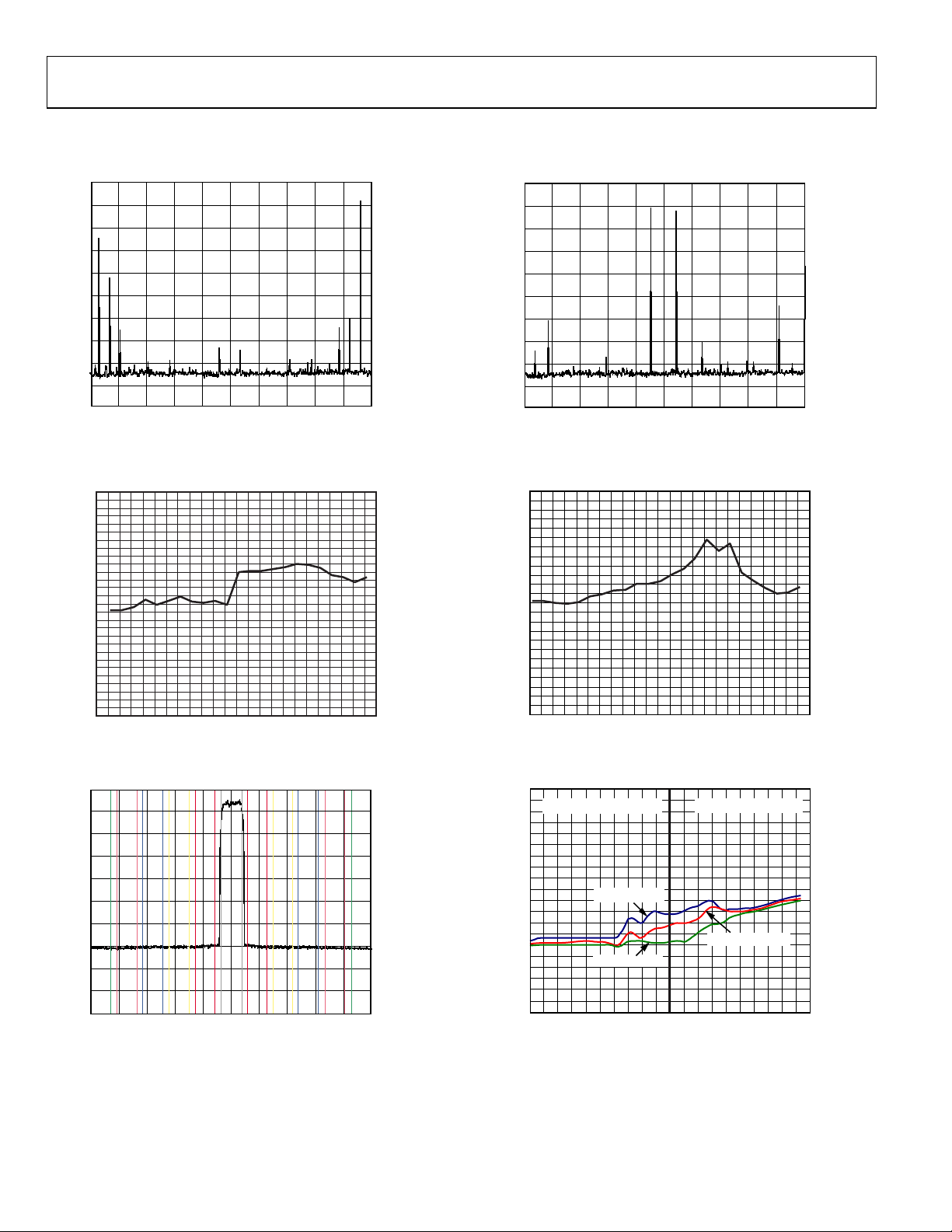
AC (MIX MODE)
f
= 2.4 GSPS, I
DAC
OUTFS
= 20 mA, nominal supplies, 25°C, unless otherwise noted.
10dB/DIV
START 20MHz
#RES BW 10kHz
Figure 25. Single-Tone Spectrum at f
80
75
70
65
60
55
50
45
40
SFDR (dBc)
35
30
25
20
15
10
1200 1300 1400 1500 1600 1700 1800 1900 2000 2100 2200 2300 2400
VBW 10kHz
f
(MHz)
OUT
= 2.31 GHz, f
OUT
Figure 26. SFDR in Mix Mode vs. f
10dB/DIV
CENTER 2.10706MHz
#RES VW 30kHz
RMS RESULTS
CARRIER PO WER
–21.43dBm/
3.84MHz
FREQ
OFFSET
(MHz)
5
10
15
20
25
VBW 300kHz
REF
BW
(MHz)
3.84
3.84
3.84
3.84
3.84
SWEEP 174.6ms ( 601pts)
LOWER
(dBc)
(dBm)
–68.99
–90.43
–72.09
–93.52
–72.86
–94.30
–74.34
–95.77
–74.77
–96.20
STOP 2.4GHz
SWEEP 28.7s (601p ts)
= 2.4 GSPS
DAC
at 2.4 GSPS
OUT
SPAN 53.84MHz
UPPER
(dBc)
(dBm)
–63.94
–90.37
–71.07
–92.50
–71.34
–92.77
–72.60
–94.03
–73.26
–94.70
09616-026
09616-032
Figure 27. Typical Single-Carrier WCDMA ACLR Performance at 2.1 GHz,
= 2457.6 MSPS (Second Nyquist Zone)
f
DAC
10dB/DIV
START 20MHz
#RES BW 10kHz
VBW 10kHz
Figure 28. Single-Tone Spectrum in Mix Mode at f
f
= 2.4 GSPS
DAC
90
85
80
75
70
65
60
55
IMD (dBc)
50
45
40
35
30
1200 1300 1400 1500 1600 1700 1800 1900 2000 2100 2200 2300 2400
f
(MHz)
09616-027
OUT
Figure 29. IMD in Mix Mode vs. f
40
SECOND NYQUIS T ZONE THIRD NYQUIST ZONE
–45
–50
–55
–60
–65
–70
ACLR (dBc)
–75
–80
–85
–90
1229 1475 1720 1966 2212 2458 2703 2949 3195 3441 3686
FIRST ADJ CH
FIFTH ADJ CH
f
OUT
(MHz)
Figure 30. Single-Carrier WCDMA ACLR vs. f
STOP 2.4GHz
STOP 2.4GHzSTART 20MHz
SWEEP 28.7s ( 601pts)
= 1.31 GHz,
OUT
at 2.4 GSPS
OUT
SECOND ADJ CH
at 2457.6 MSPS
OUT
09616-030
09616-031
09616-025
Rev. A | Page 14 of 44
 Loading...