FEATURES
Pin-compatible family
Excellent dynamic performance
AD9736: SFDR = 82 dBc at f
AD9736: SFDR = 69 dBc at f
AD9736: IMD = 87 dBc at f
AD9736: IMD = 82 dBc at f
LVDS data interface with on-chip 100 Ω terminations
Built-in self test
LVDS sampling integrity
LVDS-to-DAC data transfer integrity
Low power: 380 mW (I
= 20 mA; f
FS
1.8/3.3 V dual-supply operation
Adjustable analog output
8.66 mA to 31.66 mA (RL = 25 Ω to 50 Ω)
On-chip 1.2 V reference
160-lead chip scale ball grid array (CSP_BGA) package
APPLICATIONS
Broadband communications systems
Cellular infrastructure (digital predistortion)
Point-to-point wireless
CMTS/VOD
Instrumentation, automatic test equipment
Radar, avionics
PRODUCT DESCRIPTION
= 30 MHz
OUT
= 130 MHz
OUT
= 30 MHz
OUT
= 130 MHz
OUT
OUT
= 330 MHz)
10-, 12-, 14-Bit, 1200 MSPS DACS
AD9734/AD9735/AD9736
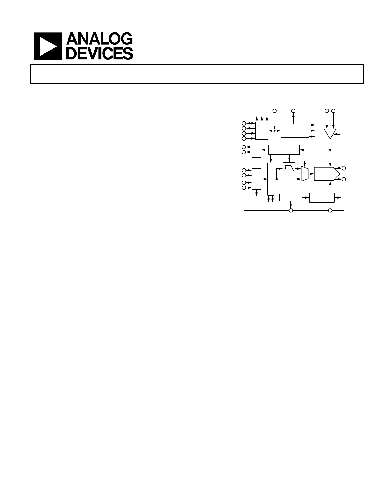
FUNCTIONAL BLOCK DIAGRAM
DACCLK–
S3
REFERENCE
CURRENT
SDI
SDO
CSB
SCLK
DATACLK_OUT+
DATACLK_OUT–
DATACLK_IN+
DATACLK_IN–
DB[13:0]+
DB[13:0]–
S1S2S3
SPI
LVDS
DRIVER
LVDS
RECEIVER
C2
RESET
CONTROLLER
CLOCK
DISTRIBUTION
SYNCHRONIZER
BAND GAP
C1S1
Figure 1.
IRQ
2×
PRODUCT HIGHLIGHTS
1. Low noise and intermodulation distortion (IMD) features
enable high quality synthesis of wideband signals at
intermediate frequencies up to 600 MHz.
2. Double data rate (DDR) LVDS data receivers support the
maximum conversion rate of 1200 MSPS.
3. Direct pin programmability of basic functions or SPI port
access for complete control of all AD973x family functions.
C1
C2
C3
14-, 12-,
10-BIT DAC
CORE
I120VREF
DACCLK+
C3
S2
IOUTA
IOUTB
04862-001
The AD9736, AD9735, and AD9734 are high performance, high
frequency DACs that provide sample rates of up to 1200 MSPS,
permitting multicarrier generation up to their Nyquist
frequency. The AD9736 is the 14-bit member of the family,
while the AD9735 and the AD9734 are the 12-bit and 10-bit
members, respectively. They include a serial peripheral interface
(SPI) port that provides for programming of many internal
parameters and also enables readback of status registers. A
reduced-specification LVDS interface is utilized to achieve the
high sample rate. The output current can be programmed
over a range of 8.66 mA to 31.66 mA. The AD973x family is
manufactured on a 0.18 µm CMOS process and operates from
1.8 V and 3.3 V supplies for a total power consumption of
380 mW in bypass mode. It is supplied in a 160-lead chip scale
ball grid array for reduced package parasitics.
Rev. 0
Information furnished by Analog Devices is believed to be accurate and reliable.
However, no responsibility is assumed by Analog Devices for its use, nor for any
infringements of patents or other rights of third parties that may result from its use.
Specifications subject to change without notice. No license is granted by implication
or otherwise under any patent or patent rights of Analog Devices. Trademarks and
registered trademarks are the property of their respective owners.
4. Manufactured on a CMOS process, the AD973x family
uses a proprietary switching technique that enhances
dynamic performance.
5. The current output(s) of the AD9736 family are easily con-
figured for single-ended or differential circuit topologies.
One Technology Way, P.O. Box 9106, Norwood, MA 02062-9106, U.S.A.
Tel: 781.329.4700
Fax: 781.461.3113 © 2005 Analog Devices, Inc. All rights reserved.
www.analog.com

AD9734/AD9735/AD9736
TABLE OF CONTENTS
DC Specifications ............................................................................. 4
Digital Specifications........................................................................ 6
AC Specifications.............................................................................. 8
Absolute Maximum Ratings............................................................ 9
ESD Caution.................................................................................. 9
Pin Configuration and Function Descriptions........................... 10
Te r mi n ol o g y .................................................................................... 13
Typical Performance Characteristics........................................... 14
AD9736 Static Linearity, 10 mA Full Scale............................. 14
AD9736 Static Linearity, 20 mA Full Scale............................. 15
AD9736 Static Linearity, 30 mA Full Scale............................. 16
AD9735 Static Linearity, 10 mA, 20 mA, 30 mA Full Scale .17
AD9734 Static Linearity, 10 mA, 20 mA, 30 mA Full Scale .18
AD9736 Power Consumption, 20 mA Full Scale................... 19
AD9736 Dynamic Performance, 20 mA Full Scale................ 19
Theory of Operation ...................................................................... 31
Serial Peripheral Interface............................................................. 32
General Operation of the Serial Interface............................... 32
Short Instruction Mode (8-Bit Instruction) ........................... 32
Long Instruction Mode (16-Bit Instruction).......................... 32
Serial Interface Port Pin Descriptions..................................... 32
MSB/LSB Transfers .................................................................... 33
Notes on Serial Port Operation ................................................ 33
Pin Mode Operation .................................................................. 34
Reset Operation.......................................................................... 34
Programming Sequence ............................................................ 34
Interpolation Filter ..................................................................... 35
Data Interface Controllers......................................................... 35
LVDS Samp l e Logic .................................................................... 36
LVDS Samp l e Logic C a l ibr ation ............................................... 36
AD9736 Dynamic Performance, 20 mA Full Scale................ 21
AD9736, AD9735, AD9734 WCDMA ACLR, 20 mA Full
.............................................................................................. 22
Scale
AD9735, AD9734 Dynamic Performance, 20 mA Full Scale24
SPI Register Map............................................................................. 25
SPI Register Descriptions.............................................................. 26
MODE Register (REG 00)......................................................... 26
Interrupt Request Register (IRQ) (Reg 01)............................. 26
Full Scale Current (FSC) Register (Regs 02, 03)..................... 27
LVDS Controller (LVDS_CNT) Register (Regs 04, 05, 06).. 27
SYNC Controller (SYNC_CNT) Register (Regs 07, 08) .......28
Cross Controller (CROS_CNT) Register (Regs 10, 11)........ 28
Analog Control (ANA_CNT) Register (Regs 14, 15)............ 29
Built-in Self Test Control (BIST_CNT) Registers (Regs 17, 18,
19, 20, 21)
Controller Clock Predivider (CCLK_DIV) Reading Register
(Reg 22)
.................................................................................... 29
........................................................................................ 30
Operating the LVDS Controller In Manual Mode via the SPI
............................................................................................... 37
Port
Operating the LVDS Controller in Surveillance and Auto
............................................................................................ 37
Mode
SYNC Logic and Controller.......................................................... 38
SYNC Logic and Controller Operation................................... 38
Operating in Manual Mode ...................................................... 38
Operation in Surveillance and Auto Modes ........................... 38
FIFO Bypass................................................................................ 38
Digital Built-In Self Test (BIST) ................................................... 40
Overview ..................................................................................... 40
AD973x BIST Procedure........................................................... 41
AD973x Expected BIST Signatures.......................................... 41
Generating Expected Signatures .............................................. 42
Cross Controller Registers............................................................. 43
Rev. 0 | Page 2 of 68

AD9734/AD9735/AD9736
Analog Control Registers...............................................................44
DAC Data Sources ..........................................................................49
Band Gap Temperature Characteristic Trim Bits ...................44
Mirror Roll-Off Frequency Control .........................................44
Headroom Bits.............................................................................44
Volt a ge R e fere n ce ........................................................................45
Applications Information...............................................................46
Driving the DACCLK Input......................................................46
DAC Output Distortion Sources ...................................................47
DC-Coupled DAC Outputs ...........................................................48
REVISION HISTORY
4/05—Revision 0: Initial Version
Input Data Timing ..........................................................................50
Synchronization Timing.................................................................51
Power Supply Sequencing ..............................................................52
AD973X Evaluation Board Schematics ........................................53
AD973X Evaluation Board PCB Layout .......................................58
Outline Dimensions........................................................................65
Ordering Guide...........................................................................65
Rev. 0 | Page 3 of 68

AD9734/AD9735/AD9736
DC SPECIFICATIONS
AVDD33 = DVDD33 = 3.3 V, CVDD18 = DVDD18 = 1.8 V, maximum sample rate, IFS = 20 mA, 1× mode, 25 Ω 1% balanced load,
unless otherwise noted.
Table 1.
AD9736 AD9735 AD9734
Parameter Min Typ Max Min Typ Max Min Typ Max Unit
RESOLUTION 14 12 10 Bits
ACCURACY
Integral Nonlinearity (INL) −5.6 ±1.0 +5.6 −1.5 ±0.50 +1.5 −0.5 ±0.12 +0.5 LSB
Differential Nonlinearity (DNL) −2.1 ±0.6 +2.1 −0.5 ±0.25 +0.5 −0.1 ±0.06 +0.1 LSB
ANALOG OUTPUTS
Offset Error −0.01 ±0.005 +0.01 −0.01 ±0.005 +0.01 −0.01 ±0.005 +0.01 % FSR
Gain Error (With Internal
Reference)
Gain Error (Without Internal
Reference)
Full-Scale Output Current 8.66 20.2 31.66 8.66 20.2 31.66 8.66 20.2 31.66 mA
Output Compliance Range −1.0 +1.0 −1.0 1.0 −1.0 +1.0 V
Output Resistance 10 10 10 MΩ
Output Capacitance 1 1 1 pF
TEMPERATURE DRIFT
Offset 0 0 0 ppm/°C
Gain 80 80 80 ppm/°C
Reference Voltage
1
REFERENCE
Internal Reference Voltage1 1.14 1.2 1.26 1.14 1.2 1.26 1.14 1.2 1.26 V
Output Resistance
2
ANALOG SUPPLY VOLTAGES
AVDD33 3.13 3.3 3.47 3.13 3.3 3.47 3.13 3.3 3.47 V
CVDD18 1.70 1.8 1.90 1.70 1.8 1.90 1.70 1.8 1.90 V
DIGITAL SUPPLY VOLTAGES
DVDD33 3.13 3.3 3.47 3.13 3.3 3.47 3.13 3.3 3.47 V
DVDD18 1.70 1.8 1.90 1.70 1.8 1.90 1.70 1.8 1.90 V
SUPPLY CURRENTS
1× Mode, 1.2 GSPS
I
AVDD33
I
CVDD18
I
DVDD33
I
DVDD18
FIR Bypass (1×) Mode 380 380 380 mW
2× Mode, 1.2 GSPS
I
AVDD33
I
CVDD18
I
DVDD33
I
DVDD18
FIR 2× Interpolation Filter
Enabled
±1.0 ±1.0 ±1.0 % FSR
±1.0 ±1.0 ±1.0 % FSR
40 40 40 ppm/°C
5 5 5 kΩ
25 25 25 mA
47 47 47 mA
10 10 10 mA
122 122 122 mA
25 25 25 mA
47 47 47 mA
10 10 10 mA
234 234 234 mA
550 550 550 mW
Rev. 0 | Page 4 of 68

AD9734/AD9735/AD9736
AD9736 AD9735 AD9734
Parameter Min Typ Max Min Typ Max Min Typ Max Unit
Static, No Clock
I
AVDD33
I
CVDD18
I
DVDD33
I
DVDD18
FIR Bypass (1×) Mode 133 133 133 mW
Sleep Mode, No Clock
I
AVDD33
FIR Bypass (1×) Mode 59 65 59 65 59 65 mW
Power-Down Mode
I
AVDD33
I
CVDD18
I
DVDD33
I
DVDD18
FIR Bypass (1×) Mode 0.12 1.24 0.12 1.24 0.12 1.24 mW
1
Default band gap adjustment (Reg0E<2:0> = 0h).
2
Use an external amplifier to drive any external load.
25 25 25 mA
8 8 8 mA
10 10 10 mA
2 2 2 mA
2.5 3.15 2.5 3.15 2.5 3.15 mA
0.01 0.13 0.01 0.13 0.01 0.13 mA
0.02 0.12 0.02 0.12 0.02 0.12 mA
0.01 0.12 0.01 0.12 0.01 0.12 mA
0.01 0.11 0.01 0.11 0.01 0.11 mA
Rev. 0 | Page 5 of 68

AD9734/AD9735/AD9736
DIGITAL SPECIFICATIONS
AVDD33 = DVDD33 = 3.3 V, CVDD18 = DVDD18 = 1.8 V, maximum sample rate, IFS = 20 mA, 1× mode, 25 Ω 1% balanced load,
unless otherwise noted.
LVDS drivers and receivers are compliant to the IEEE-1596 reduced range link, unless otherwise noted.
Table 2.
Parameter Min Typ Max Unit
LVDS DATA INPUTS
(DB[13:0]+, DB[13:0]−) DB+ = V
Input Voltage Range, Via or Vib 825 1575 mV
Input Differential Threshold, V
Input Differential Hysteresis, V
Receiver Differential Input Impedance, R
LVDS Input Rate 1200 MSPS
LVDS Minimum Data Valid Period (t
LVDS CLOCK INPUT
(DATACLK_IN+, DATACLK_IN−) DATACLK_IN+ = V
Input Voltage Range, Via or V
Input Differential Threshold1, V
Input Differential Hysteresis, V
Receiver Differential Input Impedance, R
Maximum Clock Rate 600 MHz
LVDS CLOCK OUTPUT
(DATACLK_OUT+, DATACLK_ OUT−) DATACLK_OUT+ = V
Termination
Output Voltage High, Voa or V
Output Voltage Low, Voa or V
Output Differential Voltage, |Vod| 150 200 250 mV
Output Offset Voltage, V
Output Impedance, Single-Ended, R
Ro Mismatch Between A and B, ∆R
Change in |Vod| Between 0 and 1, |∆Vod|
Change in Vos Between 0 and 1, ∆V
Output Current—Driver Shorted to Ground, Isa, I
Output Current—Drivers Shorted Together, I
Power-Off Output Leakage, |Ixa|, |Ixb| 10 mA
Maximum Clock Rate 600 MHz
DAC CLOCK INPUT (CLK+, CLK−)
Input Voltage Range, CLK– or CLK+ 0 800
Differential Peak-to-Peak Voltage 400 800 1600 mV
Common-Mode Voltage 300 400 500 mV
Maximum Clock Rate 1200 MHz
SERIAL PERIPHERAL INTERFACE
Maximum Clock Rate (f
Minimum Pulse Width High, t
Minimum Pulse Width Low, t
Minimum SDIO and CSB to SCLK Setup, t
Minimum SCLK to SDIO Hold, t
Maximum SCLK to Valid SDIO and SDO, t
Minimum SCLK to Invalid SDIO and SDO, t
, DB- = Vib
ia
idth
– V
idthh
idthl
in
) 344 ps
MDE
, DATACLK_IN− = V
ia
ib
idth
- V
idthh
idthl
in
, DATACLK_OUT− = Vob 100 Ω
oa
ib
−100 +100 mV
20 mV
80 120 Ω
825 1575 mV
−100 +100 mV
20 mV
80 120 Ω
ob
ob
os
o
o
1375 mV
1025 mV
1150 1250 mV
80 100 120 Ω
10 %
25 mV
SCLK
os
sb
sab
, 1/t
) 20 MHz
SCLK
PWH
PWL
DS
DH
DV
DNV
25 mV
20 mA
4 mA
20 ns
20 ns
10 ns
5 ns
20 ns
5 ns
Rev. 0 | Page 6 of 68

AD9734/AD9735/AD9736
Parameter Min Typ Max Unit
INPUTS (SDI, SDIO, SCLK, CSB)
Voltage in High, V
Voltage in Low, V
Current in High, I
Current in Low, I
ih
il
ih
il
Input Capacitance pF
SDIO OUTPUT
Voltage out High, V
Voltage out Low, V
Current out High, I
Current out Low, I
1
Refer to the section for recommended LVDS differential drive levels. Input Data Timing
oh
ol
oh
ol
2.0 3.3 V
0 0.8 V
−10 +10 µA
−10 +10 µA
2.4 3.6 V
0 0.4 V
4 mA
4 mA
Rev. 0 | Page 7 of 68

AD9734/AD9735/AD9736
AC SPECIFICATIONS
AVDD33 = DVDD33 = 3.3 V, CVDD18 = DVDD18 = 1.8 V, maximum sample rate, IFS = 20 mA, 1× mode, 25 Ω 1% balanced load,
unless otherwise noted.
Table 3.
AD9736 AD9735 AD9734
Parameter Min Typ Max Min Typ Max Min Typ Max Unit
DYNAMIC PERFORMANCE
Maximum Update Rate 1200 1200 1200 MSPS
SPURIOUS-FREE DYNAMIC RANGE (SFDR)
f
= 800 MSPS
DAC
f
= 20 MHz 75 75 75 dBc
OUT
f
= 1200 MSPS
DAC
f
= 50 MHz 80 76 76 dBc
OUT
f
= 100 MHz 77 74 71 dBc
OUT
f
= 316 MHz 63 63 60 dBc
OUT
f
= 550 MHz 55 54 53 dBc
OUT
TWO-TONE INTERMODULATION
DISTORTION (IMD)
f
= 1200 MSPS
DAC
f
= f
OUT2
+ 1.25 MHz
OUT
f
= 40 MHz 88 84 83 dBc
OUT
f
= 50 MHz 85 84 83 dBc
OUT
f
= 100 MHz 84 81 79 dBc
OUT
f
= 315 MHz 70.5 67 66 dBc
OUT
f
= 550 MHz 65 60 60 dBc
OUT
NOISE SPECTRAL DENSITY (NSD)
Single Tone
f
= 1200 MSPS
DAC
f
= 50 MHz −165
OUT
f
= 100 MHz −164 −161 −154 dBm/Hz
OUT
f
= 241MHz −158.5 −160.5 −159.5 −155 dBm/Hz
OUT
f
= 316 MHz −158 −157 −152 dBm/Hz
OUT
f
= 550 MHz −155 −155 −149 dBm/Hz
OUT
Eight-Tone
f
= 1200 MSPS, 500 kHz Tone
DAC
Spacing
f
= 50 MHz −166.5 −163 −154 dBm/Hz
OUT
f
= 100 MHz −166 −163 −152 dBm/Hz
OUT
f
= 241MHz −163.3 −165 −161.5 −150.5 dBm/Hz
OUT
f
= 316 MHz −164 −162 −151 dBm/Hz
OUT
f
= 550 MHz −162 −160 −150 dBm/Hz
OUT
−162
−154 dBm/Hz
Rev. 0 | Page 8 of 68
AD9734/AD9735/AD9736
ABSOLUTE MAXIMUM RATINGS
Table 4.
With
Parameter
AVDD33 AVSS −0.3 V +3.6 V
DVDD33 DVSS −0.3 V +3.6 V
DVDD18 DVSS −0.3 V +1.98 V
CVDD18 CVSS −0.3 V +1.98 V
AVSS DVSS −0.3 V +0.3 V
AVSS CVSS −0.3 V +0.3 V
DVSS CVSS −0.3 V +0.3 V
CLK+, CLK− CVSS −0.3 V CVDD18 + 0.18 V
PIN_MODE DVSS −0.3 V DVDD33 + 0.3 V
DATACLK_IN,
DATACLK_OUT
LVDS Data Inputs DVSS −0.3 V DVDD33 + 0.3 V
IOUTA, IOUTB AVSS −1.0 V AVDD33 + 0.3 V
I120, VREF, IPTAT AVSS −0.3 V AVDD33 + 0.3 V
IRQ, CSB, SCLK,
SDO, SDIO, RESET DVSS −0.3 V DVDD33 + 0.3 V
Junction Temp. 150°C
Storage Temp. −65°C +150°C
Respect to
DVSS −0.3 V DVDD33 + 0.3 V
Min Max
Stresses above those listed under Absolute Maximum Ratings
may cause permanent damage to the device. This is a stress
rating only; functional operation of the device at these or any
other conditions above those indicated in the operational
sections of this specification is not implied. Exposure to
absolute maximum ratings for extended periods may effect
device reliability.
ESD CAUTION
ESD (electrostatic discharge) sensitive device. Electrostatic charges as high as 4000 V readily accumulate on
the human body and test equipment and can discharge without detection. Although this product features
proprietary ESD protection circuitry, permanent damage may occur on devices subjected to high energy
electrostatic discharges. Therefore, proper ESD precautions are recommended to avoid performance
degradation or loss of functionality.
Note that this device in its current form does not meet Analog Devices’ standard requirements for ESD as measured against the charged
device model (CDM). As such, special care should be used when handling this product, especially in a manufacturing environment. Analog
Devices will provide a more ESD-hardy product in the near future at which time this warning will be removed from this datasheet.
Rev. 0 | Page 9 of 68
AD9734/AD9735/AD9736
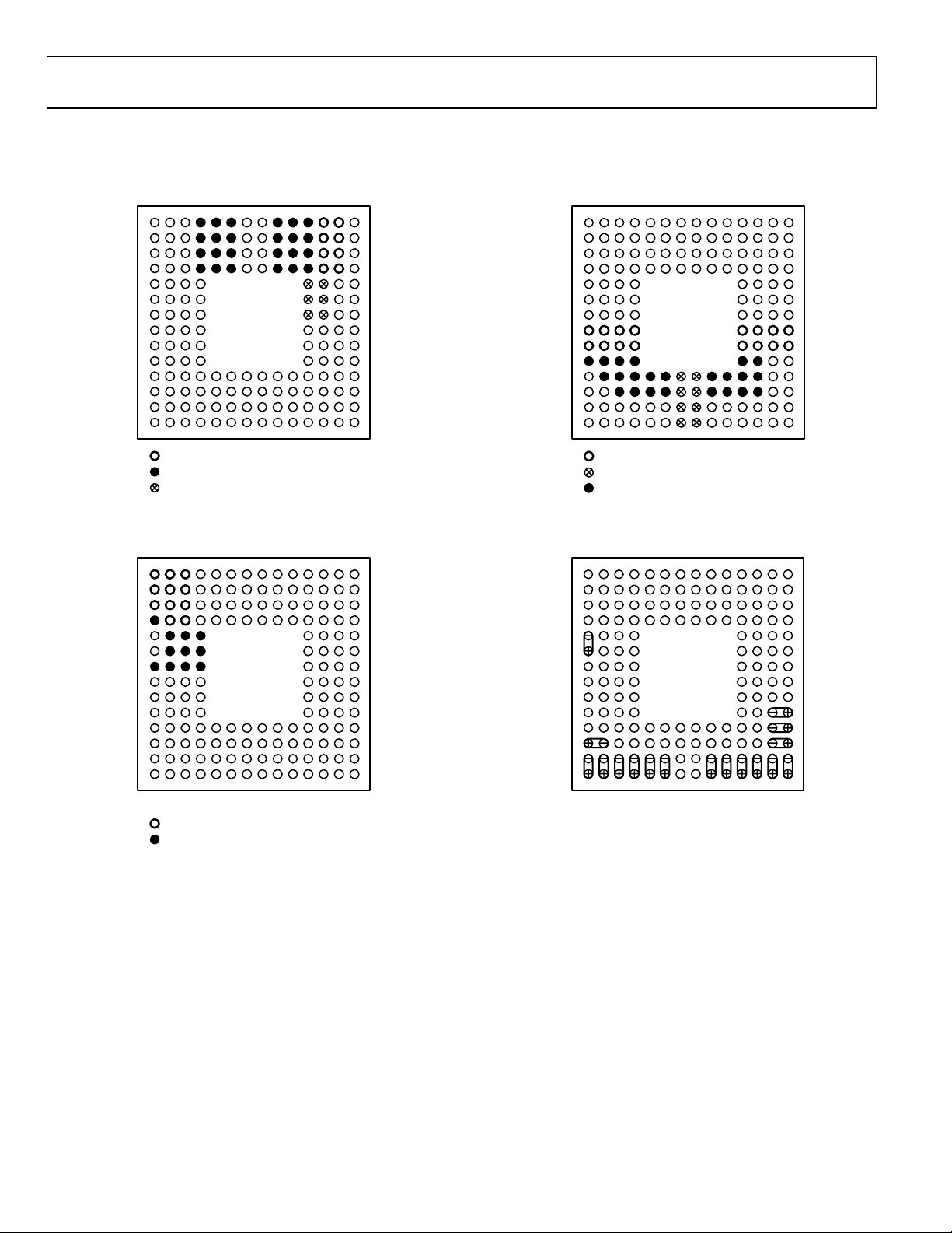
PIN CONFIGURATION AND FUNCTION DESCRIPTIONS
1413121110876321954
1413121110876321954
A
B
C
D
E
F
G
H
J
K
L
M
N
P
AVDD33, 3.3V, ANALOG SUPPLY
AVSS, ANALOG SUPPLY GROUND
AVSS, ANALOG SUPPLY GROUND SHIELD
Figure 2. AD9736 Analog Supply Pins ( Top View)
A
B
C
D
E
F
G
H
J
K
L
M
N
P
A
B
C
D
E
F
G
H
J
K
L
M
N
P
DVDD18, 1.8V DIGITAL SUPPLY
DVDD33, 3.3V DIGITAL SUPPLY
04862-002
DVSS DIGITAL SUPPLY GROUND
04862-004
Figure 4. AD9736 Digital Supply Pins ( Top View)
1413121110876321954
A
B
C
D
E
CLK–
F
CLK+
G
H
J
K
L
MDB0 (LSB)
N
P
1413121110876321954
DB13 (MSB)
DB12
DB11
CVDD18, 1.8V CLOCK SUPPLY
CVSS, CLOCK SUPPLY GROUND
Figure 3. AD9736 Clock Supply Pins ( Top View)
04862-003
DB1
DATACLK_OUT
DB6
DATACLK_IN
Figure 5. AD9736 Digital LVDS Inputs, Clock I/O (Top View)
DB7
DB8
DB9
DB10
04862-005
DB5
DB4
DB3
DB2
Rev. 0 | Page 10 of 68
AD9734/AD9735/AD9736
IOUTB
IOUTA
1413121110876321954
PIN_MODE
A
B
C
D
E
F
G
H
J
K
L
M
N
P
I120
VREF
IPTAT
CSB
SCLK
UNSIGNED
FSC0
PIN_MODE = 0,
SPI ENABLED
IRQ
PIN_MODE = 1,
SPI DISABLED
2×
RESET
SDIO
SDO
PD
FIFO
FSC1
04862-006
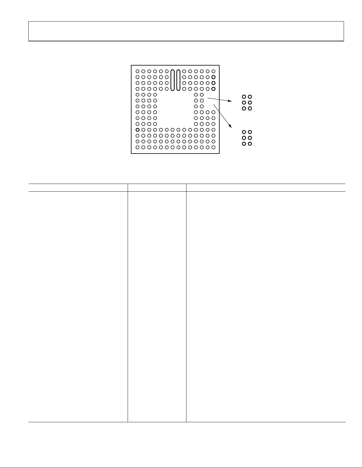
Figure 6. AD9736 Analog I/O and SPI Control Pins ( Top View)
Table 5. Pin Function Descriptions
Pin No. Mnemonic Description
A1, A2, A3, B1, B2, B3, C1, C2, C3, D2, D3 CVDD18 1.8 V Clock Supply.
A4, A5, A6, A9, A10, A11, B4, B5, B6, B9,
AVSS Analog Supply Ground.
B10, B11, C4, C5, C6, C9, C10, C11, D4, D5,
D6, D9, D10, D11
A7, B7, C7, D7 IOUTB DAC Negative Output; 10 mA to 30 mA full-scale output current.
A8, B8, C8, D8 IOUTA DAC Positive Output; 10 mA to 30 mA full-scale output current.
A12, A13, B12, B13, C12, C13, D12, D13 AVDD33 3.3 V Analog Supply.
A14 DNC Do Not Connect.
B14 I120
Nominal 1.2 V Reference; tie to analog ground via 10 kΩ resistor to
generate a 120 µA reference current.
C14 VREF
Band Gap Voltage Reference I/O; tie to analog ground via 1 nF
capacitor, output impedance approximately 5 kΩ.
D1, E2, E3, E4, F2, F3, F4, G1, G2, G3, G4 CVSS Clock Supply Ground.
D14 IPTAT
Factory Test Pin; output current proportional to absolute
temperature, approximately 10 µA at 25°C with approximately
20 nA/°C slope.
E1, F1 DACCLK−/DACCLK+ Negative/Positive DAC Clock Input (DACCLK).
E11, E12, F11, F12, G11, G12 AVSS Analog Supply Ground Shield; tie to AVSS at the DAC.
E13 IRQ/UNSIGNED
If PIN_MODE = 0, IRQ: Active low open-drain interrupt request
output, pull up to DVDD33 with 10 kΩ resistor.
If PIN_MODE = 1, UNSIGNED: Digital input pin where 0 = twos
complement input data format, 1 = unsigned.
E14 RESET/PD If PIN_MODE = 0, RESET: 1 resets the AD9736.
If PIN_MODE = 1, PD: 1 puts the AD9736 in the power-down state.
F13 CSB/2×
See Serial Peripheral Interface and Pin Mode Operation sections for
pin description.
F14 SDIO/FIFO See the Pin Mode Operation section for pin description.
G13 SCLK/FSC0 See the Pin Mode Operation section for pin description.
G14 SDO/FSC1 See the Pin Mode Operation section for pin description.
H1, H2, H3, H4, H11, H12, H13, H14, J1, J2,
DVDD18 1.8 V Digital Supply.
J3, J4, J11, J12, J13, J14
K1, K2, K3, K4, K11, K12, L2, L3, L4, L5, L6,
DVSS Digital Supply Ground.
L9, L10, L11, L12, M3, M4, M5, M6, M9,
M10, M11, M12
Rev. 0 | Page 11 of 68

AD9734/AD9735/AD9736
Pin No. Mnemonic Description
K13, K14 DB<13>−/DB<13>+ Negative/Positive Data Input Bit 13 (MSB); reduced swing LVDS.
L1 PIN_MODE 0 = SPI Mode; SPI enabled.
1 = PIN Mode; SPI disabled, direct pin control.
L7, L8, M7, M8, N7, N8, P7, P8 DVDD33 3.3 V Digital Supply.
L13, L14 DB<12>−/DB<12>+ Negative/Positive Data Input Bit 12; reduced swing LVDS.
M2, M1 DB<0>−/DB<0>+ Negative/Positive Data Input Bit 0 (LSB); reduced swing LVDS.
M13, M14 DB<11>−/DB<11>+ Negative/Positive Data Input Bit 11; reduced swing LVDS.
N1, P1 DB<1>−/DB<1>+ Negative/Positive Data Input Bit 1; reduced swing LVDS.
N2, P2 DB<2>−/DB<2>+ Negative/Positive Data Input Bit 2; reduced swing LVDS.
N3, P3 DB<3>−/DB<3>+ Negative/Positive Data Input Bit 3; reduced swing LVDS.
N4, P4 DB<4>−/DB<4>+ Negative/Positive Data Input Bit 4; reduced swing LVDS..
N5, P5 DB<5>−/DB<5>+ Negative/Positive Data Input Bit 5; reduced swing LVDS.
N6, P6 DATACLK_OUT−/
DATACLK_OUT+
N9, P9 DATACLK_IN−/
DATACLK_IN+
N10, P10 DB<6>−/DB<6>+ Negative/Positive Data Input Bit 6; reduced swing LVDS.
N11, P11 DB<7>−/DB<7>+ Negative/Positive Data Input Bit 7; reduced swing LVDS.
N12, P12 DB<8>−/DB<8>+ Negative/Positive Data Input Bit 8; reduced swing LVDS.
N13, P13 DB<9>−/DB<9>+ Negative/Positive Data Input Bit 9; reduced swing LVDS.
N14, P14 DB<10>−/DB<10>+ Negative/Positive Data Input Bit 10; reduced swing LVDS.
Negative/Positive Data Output Clock; reduced swing LVDS.
Negative/Positive Data Input Clock; reduced swing LVDS
Rev. 0 | Page 12 of 68

AD9734/AD9735/AD9736
TERMINOLOGY
Linearity Error (Integral Nonlinearity or INL)
The maximum deviation of the actual analog output from the
ideal output, determined by a straight line drawn from zero to
full scale.
Power Supply Rejection
The maximum change in the full-scale output as the supplies
are varied from nominal to minimum and maximum specified
voltages.
Differential Nonlinearity (DNL)
The measure of the variation in analog value, normalized to full
scale, associated with a 1 LSB change in digital input code.
Monotonicity
A DAC is monotonic if the output either increases or remains
constant as the digital input increases.
Offset Error
The deviation of the output current from the ideal of zero is
called the offset error. For IOUTA, 0 mA output is expected
when the inputs are all 0s. For IOUTB, 0 mA output is expected
when all inputs are set to 1s.
Gain Error
The difference between the actual and ideal output span. The
actual span is determined by the output when all inputs are set
to 1s minus the output when all inputs are set to 0s.
Output Compliance Range
The range of allowable voltage at the output of a current output
DAC. Operation beyond the maximum compliance limits may
cause either output stage saturation or breakdown, resulting in
nonlinear performance.
Temp er at u re D ri ft
Specified as the maximum change from the ambient (25°C)
value to the value at either T
drift, the drift is reported in ppm of full-scale range (FSR)
per °C. For reference drift, the drift is reported in ppm per °C.
MIN
or T
. For offset and gain
MAX
Settling Time
The time required for the output to reach and remain within a
specified error band about its final value, measured from the
start of the output transition.
Glitch Impulse
Asymmetrical switching times in a DAC give rise to undesired
output transients that are quantified by a glitch impulse. It is
specified as the net area of the glitch in pV-s.
Spurious-Free Dynamic Range
The difference, in dB, between the rms amplitude of the output
signal and the peak spurious signal over the specified bandwidth.
Total Harmonic Distortion (THD)
THD is the ratio of the rms sum of the first six harmonic
components to the rms value of the measured input signal. It is
expressed as a percentage or in decibels (dB).
Multitone Power Ratio
The spurious-free dynamic range containing multiple carrier
tones of equal amplitude. It is measured as the difference
between the rms amplitude of a carrier tone to the peak
spurious signal in the region of a removed tone.
Rev. 0 | Page 13 of 68
AD9734/AD9735/AD9736
TYPICAL PERFORMANCE CHARACTERISTICS
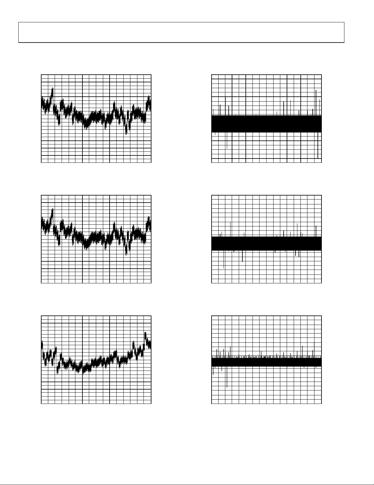
AD9736 STATIC LINEARITY, 10 mA FULL SCALE
1.00
0.75
0.50
0.25
0
–0.25
–0.50
–0.75
ERROR (LSB)
–1.00
–1.25
–1.50
–1.75
–2.00
–0.25
–0.50
–0.75
ERROR (LSB)
–1.00
–1.25
–1.50
–1.75
–2.00
–0.25
–0.50
–0.75
ERROR (LSB)
–1.00
–1.25
–1.50
–1.75
–2.00
CODE
Figure 7. AD9736 INL, −40°C, 10 mA FS
1.00
0.75
0.50
0.25
0
CODE
Figure 8. AD9736 INL, 25°C, 10 mA FS
1.00
0.75
0.50
0.25
0
CODE
Figure 9. AD9736 INL, 85°C, 10 mA FS
163840 2048 4096 6144 8192 10240 12288 14336
04862-008
163840 2048 4096 6144 8192 10240 12288 14336
04862-008
163840 2048 4096 6144 8192 10240 12288 14336
04862-009
1.0
0.8
0.6
0.4
0.2
0
–0.2
ERROR (LSB)
–0.4
–0.6
–0.8
–1.0
CODE
163840 2048 4096 6144 8192 10240 12288 14336
04862-010
Figure 10. AD9736 DNL, −40°C, 10 mA FS
1.0
0.8
0.6
0.4
0.2
0
–0.2
ERROR (LSB)
–0.4
–0.6
–0.8
–1.0
CODE
163840 2048 4096 6144 8192 10240 12288 14336
04862-011
Figure 11. AD976 DNL, 25°C, 10 mA FS
1.0
0.8
0.6
0.4
0.2
0
–0.2
ERROR (LSB)
–0.4
–0.6
–0.8
–1.0
CODE
163840 2048 4096 6144 8192 10240 12288 14336
04862-012
Figure 12. AD9736 DNL, 85°C, 10 mA FS
Rev. 0 | Page 14 of 68

AD9734/AD9735/AD9736
AD9736 STATIC LINEARITY, 20 mA FULL SCALE
1.0
0.8
0.6
0.4
0.2
0
–0.2
–0.4
ERROR (LSB)
–0.6
–0.8
–1.0
–1.2
–1.4
CODE
163840 2048 4096 6144 8192 10240 12288 14336
04862-013
Figure 13. AD9736 INL, −40°C, 20 mA FS
1.0
0.8
0.6
0.4
0.2
0
–0.2
–0.4
ERROR (LSB)
–0.6
–0.8
–1.0
–1.2
–1.4
CODE
163840 2048 4096 6144 8192 10240 12288 14336
04862-014
Figure 14. AD9736 INL, 25°C, 20 mA FS
1.0
0.8
0.6
0.4
0.2
0
–0.2
–0.4
ERROR (LSB)
–0.6
–0.8
–1.0
–1.2
–1.4
CODE
163840 2048 4096 6144 8192 10240 12288 14336
04862-015
Figure 15. AD9736 INL, 85°C, 20 mA FS
0.6
0.5
0.4
0.3
0.2
0.1
0
–0.1
ERROR (LSB)
–0.2
–0.3
–0.4
–0.5
–0.6
CODE
163840 2048 4096 6144 8192 10240 12288 14336
04862-016
Figure 16. AD9736 DNL, −40°C, 20 mA FS
0.6
0.5
0.4
0.3
0.2
0.1
0
–0.1
ERROR (LSB)
–0.2
–0.3
–0.4
–0.5
–0.6
CODE
163840 2048 4096 6144 8192 10240 12288 14336
04862-017
Figure 17. AD9736 DNL, 25°C, 20 mA FS
0.6
0.5
0.4
0.3
0.2
0.1
0
–0.1
ERROR (LSB)
–0.2
–0.3
–0.4
–0.5
–0.6
CODE
163840 2048 4096 6144 8192 10240 12288 14336
04862-018
Figure 18. AD9736 DNL, 85°C, 20 mA FS
Rev. 0 | Page 15 of 68
AD9734/AD9735/AD9736
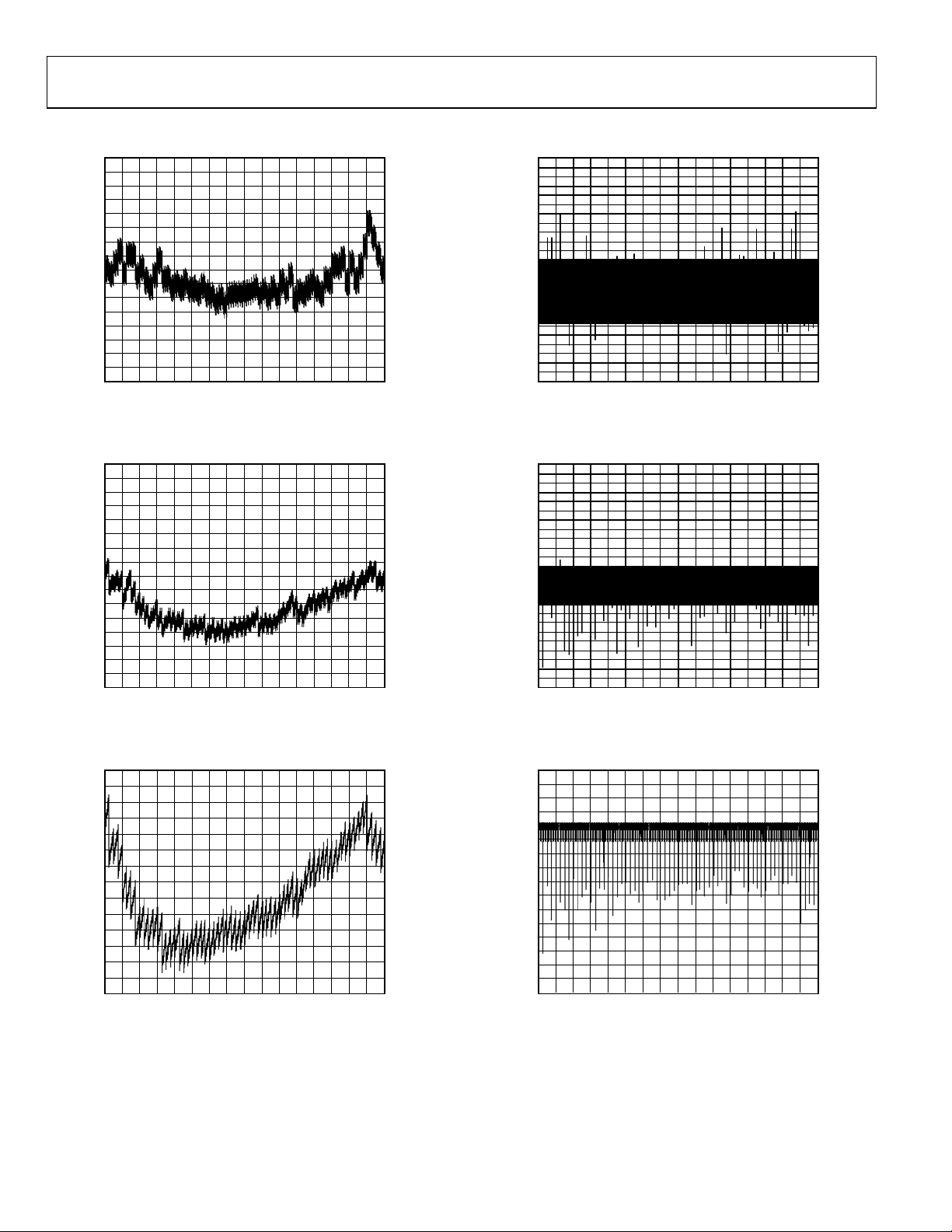
AD9736 STATIC LINEARITY, 30 mA FULL SCALE
2.0
1.5
1.0
0.5
0
–0.5
ERROR (LSB)
–1.0
–1.5
–2.0
CODE
Figure 19. AD9736 INL, −40°C, 30 mA FS
2.0
1.5
1.0
0.5
0
–0.5
ERROR (LSB)
–1.0
–1.5
–2.0
CODE
Figure 20. AD9736 INL, 25°C, 30 mA FS
2.0
1.5
1.0
0.5
0
0
0
0
–0.5
–0.5
ERROR (LSB)
–1.0
–1.0
–1.5
–1.5
–2.0
CODE
Figure 21. AD9736 INL, 85°C, 30 mA FS
163840 2048 4096 6144 8192 10240 12288 14336
163840 2048 4096 6144 8192 10240 12288 14336
163840 2048 4096 6144 8192 10240 12288 14336
04862-019
04862-020
04862-021
0.6
0.5
0.4
0.3
0.2
0.1
0
–0.1
ERROR (LSB)
–0.2
–0.3
–0.4
–0.5
–0.6
CODE
163840 2048 4096 6144 8192 10240 12288 14336
04862-022
Figure 22. AD9736 DNL, −40°C, 30 mA FS
0.6
0.5
0.4
0.3
0.2
0.1
0
–0.1
ERROR (LSB)
–0.2
–0.3
–0.4
–0.5
–0.6
CODE
163840 2048 4096 6144 8192 10240 12288 14336
04862-023
Figure 23. AD9736 DNL, 25°C, 30 mA FS
1.0
0.5
0
–0.5
–1.0
–1.5
ERROR (LSB)
–2.0
–2.5
–3.0
CODE
163840 2048 4096 6144 8192 10240 12288 14336
04862-024
Figure 24. AD9736 DNL, 85°C, 30 mA FS
Rev. 0 | Page 16 of 68
AD9734/AD9735/AD9736
–
–
–
–
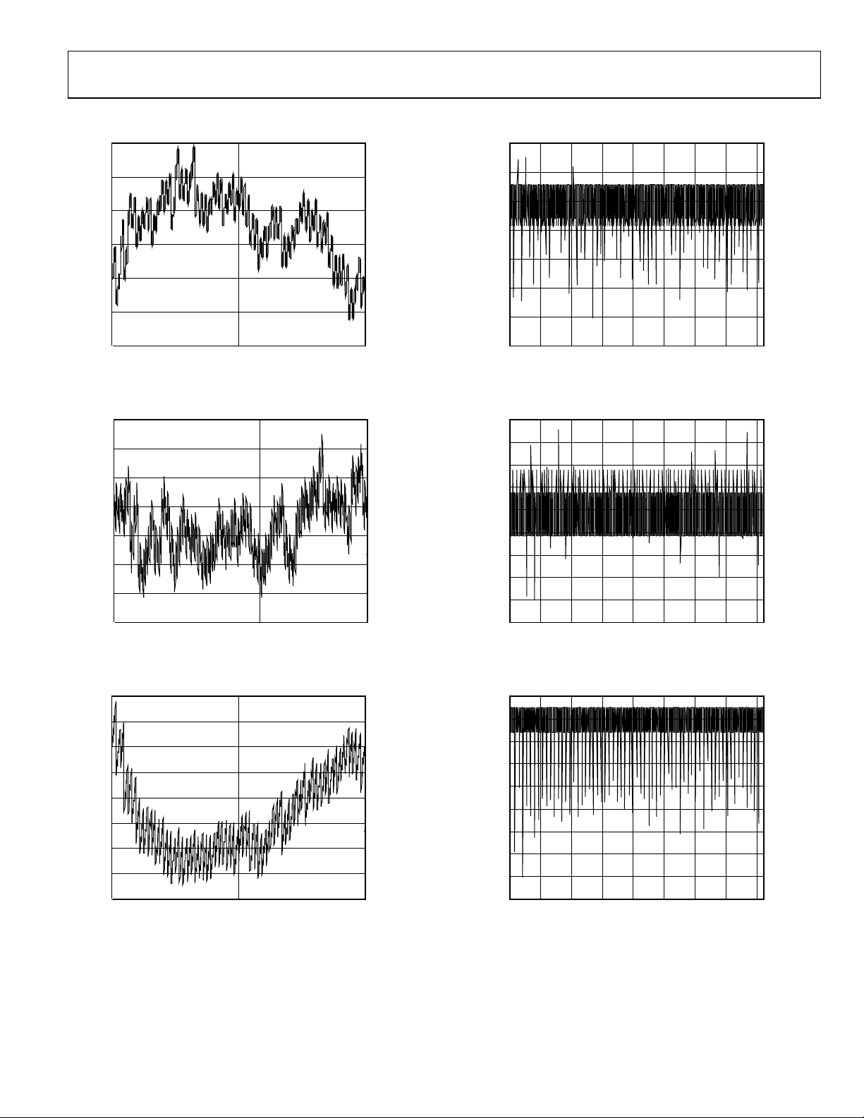
AD9735 STATIC LINEARITY, 10 mA, 20 mA, 30 mA FULL SCALE
0.4
0.100
0.3
0.2
0.1
–0.1
–0.2
0.15
0.10
0.05
0.05
0.10
0.15
0.20
0.2
0.1
–0.1
–0.2
–0.3
–0.4
–0.5
–0.6
0.050
0
–0.050
–0.100
0
40950 2341
04862-025
Figure 25. AD9735 INL, 25°C, 10 mA FS
0
40950 2341
04862-026
Figure 26. AD9735 INL, 25°C, 20 mA FS
0
40950 2341
04862-027
Figure 27. AD9735 INL, 25°C, 30 mA FS
–0.150
–0.200
–0.250
0.100
0.075
0.050
0.025
–0.025
–0.050
–0.075
–0.100
–0.125
0.050
–0.050
–1.000
–1.150
–0.200
–0.250
–0.300
–0.350
–0.400
40950 500 1000 1500 2000 2500 3000 3500
04862-028
Figure 28. AD9735 DNL, 25°C, 10 mA FS
0
40950 500 1000 1500 2000 2500 3000 3500
04862-029
Figure 29. AD9735 DNL, 25°C, 20 mA FS
0
40950 500 1000 1500 2000 2500 3000 3500
04862-030
Figure 30. AD9735 DNL, 25°C, 30 mA FS
Rev. 0 | Page 17 of 68
AD9734/AD9735/AD9736
–
–
–
–
–
–
–
–
–
–
–
–
–
–
–
–
–
–
–
–
–
–
–
–
–
–
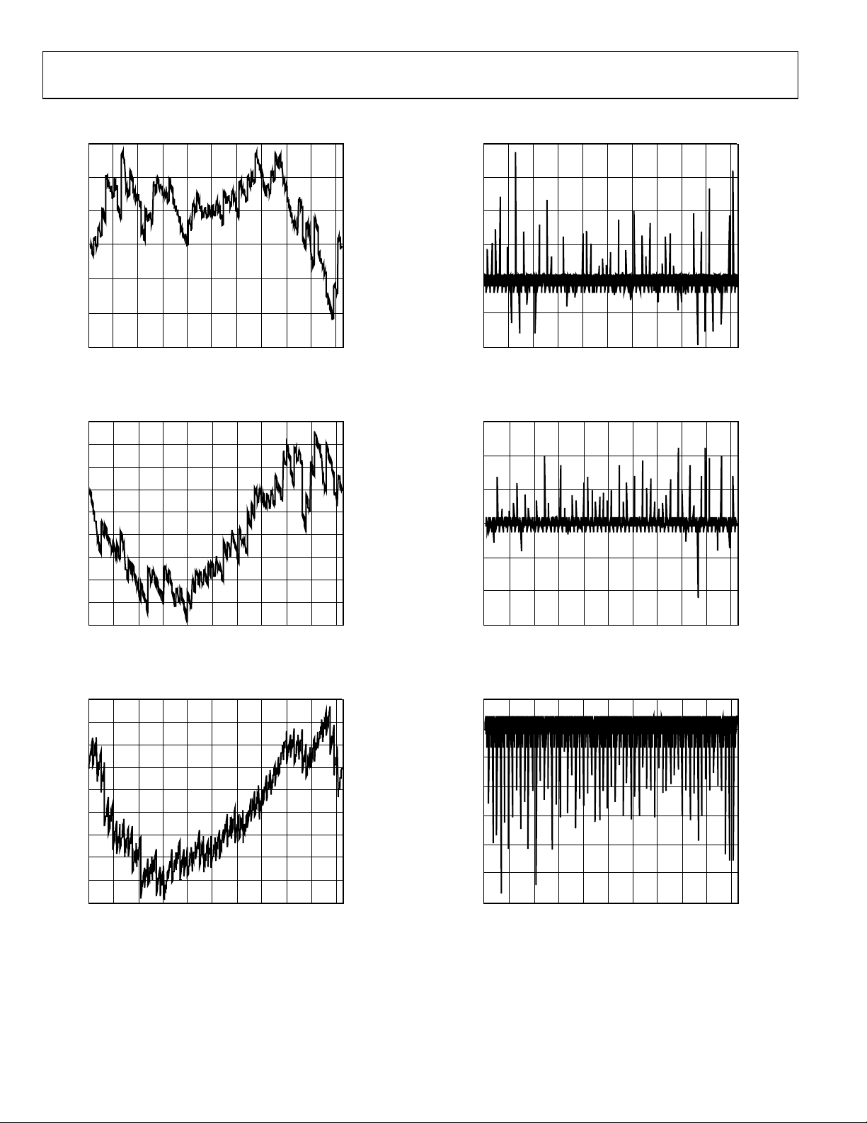
AD9734 STATIC LINEARITY, 10 mA, 20 mA, 30 mA FULL SCALE
0.06
0.04
0.04
0.02
0.02
0.04
0.06
0.03
0.02
0.01
0.01
0.02
0.03
0.04
0.05
0.06
0.06
0.04
0.02
0.02
0.04
0.06
0.08
0.10
0.12
0.03
0.02
0
10230 100 200 300 400 500 600 800 900700
04862-031
Figure 31. AD9734 INL, 25°C, 10 mA FS
0
10230 100 200 300 400 500 600 800 900700
04862-032
Figure 32. AD9734 INL, 25°C, 20 mA FS
0
10230 100 200 300 400 500 600 800 900700
04862-033
Figure 33. AD9734 INL, 25°C, 30 mA FS
0.01
0.01
0.02
0.03
0.02
0.01
0.01
0.02
0.03
0.01
0.01
0.02
0.03
0.04
0.05
0.06
0
10230 100 200 300 400 500 600 800 900700
04862-034
Figure 34. AD9734 DNL, 25°C, 10 mA FS
0
10230 100 200 300 400 500 600 800 900700
04862-035
Figure 35. AD9734 DNL, 25°C, 20 mA FS
0
10230 100 200 300 400 500 600 800 900700
04862-036
Figure 36. AD9734 DNL, 25°C, 30 mA FS
Rev. 0 | Page 18 of 68
AD9734/AD9735/AD9736
AD9736 POWER CONSUMPTION, 20 mA FULL SCALE
0.50
0.45
0.40
0.35
0.30
0.25
0.20
POWER (W)
0.15
0.10
0.05
0
f
DAC
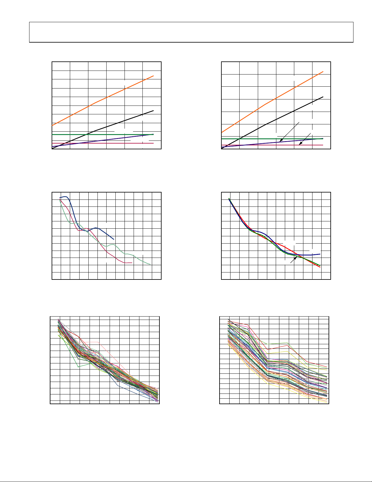
Figure 37. AD9736 1× Mode Power vs. f
(MHz)
TOTAL
AVDD33
DVDD18
CVDD18
DVDD33
at 25°C
DAC
15000 250 500 750 1000 1250
04862-037
AD9736 DYNAMIC PERFORMANCE, 20 mA FULL SCALE
80
0.7
0.6
0.5
0.4
0.3
POWER (W)
0.2
0.1
0
AVDD33
f
DAC
(MHz)
TOTAL
Figure 38. AD9736, 2× Interpolation Mode Power vs. f
80
DVDD18
VCDD18
DVDD33
DAC
15000 250 500 750 1000 1250
04862-038
at 25°C
75
70
65
SFDR (dBc)
60
55
50
Figure 39. AD9736 SFDR vs. f
78
76
74
72
70
68
66
64
SFDR (dBc)
62
60
58
56
54
52
Figure 41. AD9736 SFDR vs. f
800MSPS
1.2GSPS
1GSPS
f
(MHz)
OUT
over f
OUT
DAC
f
(MHz)
OUT
over 50 parts, 25°C, 1.2 GSPS
OUT
at 25°C
75
70
65
SFDR (dBc)
60
55
6000 50 100 150 200 250 300 350 400 450 500 550
04862-039
50
Figure 40. AD9736 SFDR vs. f
92
90
88
86
84
82
80
78
76
74
IMD (dBc)
72
70
68
66
64
62
60
5500 50 100 150 200 250 300 350 400 450 500
04862-041
58
f
Figure 42. AD9736 IMD vs. f
+85°C
+25°C
f
(MHz)
OUT
over Temperature
OUT
(MHz)
OUT
over 50 parts, 25°C,1.2 GSPS
OUT
–40°C
6000 50 100 150 200 250 300 350 400 450 500 550
04862-040
5500 50 100 150 200 250 300 350 400 450 500
04862-042
Rev. 0 | Page 19 of 68
AD9734/AD9735/AD9736
90
85
80
1GSPS
90
85
80
THIRD-ORDER IMD
SFDR
75
70
IMD (dBc)
65
60
55
50
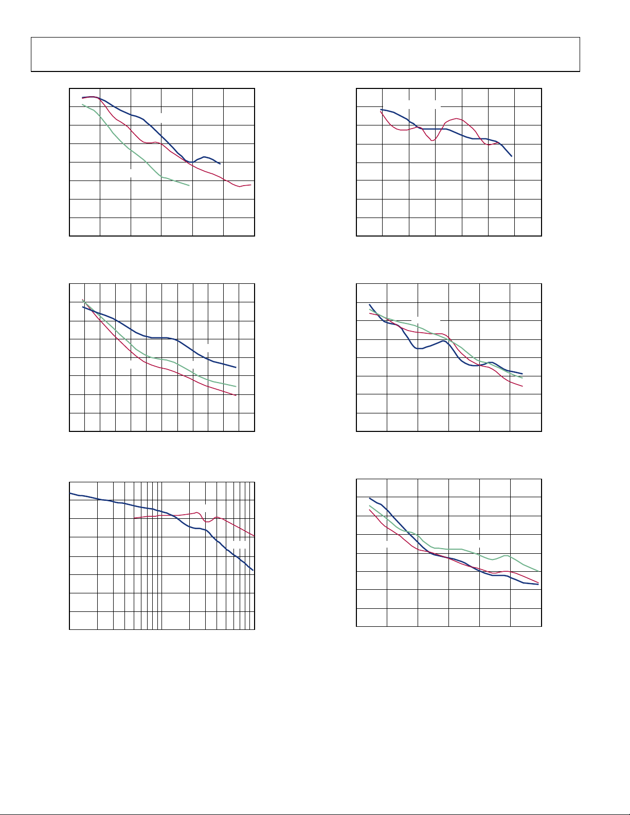
Figure 43. AD9736 IMD vs. f
90
85
80
75
70
IMD (dBc)
65
60
55
50
Figure 44. AD9736 IMD vs. f
95
90
85
80
75
70
IMD AND SFDR (dBc)
65
60
55
800MSPS
+85°C
f
(MHz)
OUT
over f
OUT
DAC
–40°C
+25°C
f
(MHz)
OUT
over Temperature, 1.2 GSPS
OUT
IMD
f
(MHz)
OUT
Figure 45. AD9736 Low Frequency IMD and SFDR vs. f
1.2GSPS
at 25°C
SFDR
, 25°C, 1.2 GSPS
OUT
75
70
65
SFDR, IMID (dBc)
60
55
6000 100 200 300 400 500
04862-043
6000 100 200 300 400 500
04862-044
100010
04862-045
50
f
OUT
Figure 46. AD9736 IMD and SFDR vs. f
80
75
70
65
60
55
SFDR (dBc)
50
45
40
0dBFS
–12dBFS
f
OUT
Figure 47. AD9736 SFDR vs. f
90
85
80
75
70
IMD (dBc)
65
60
55
50
0dBFS
–6dBFS
f
OUT
Figure 48. AD9736 IMD vs. f
(MHz)
, 25°C, 1.2 GSPS, 2× Interpolation
OUT
–6dBFS
(MHz)
OUT
(MHz)
OUT
over A
over A
–12dBFS
, 25°C, 1.2 GSPS
OUT
, 25°C, 1.2 GSPS
OUT
3500 50 100 150 200 250 300
04862-046
6000 100 200 300 400 500
04862-047
6000 100 200 300 400 500
04862-048
Rev. 0 | Page 20 of 68
AD9734/AD9735/AD9736
AD9736 DYNAMIC PERFORMANCE, 20 mA FULL SCALE
90
85
80
75
70
65
SFDR, IMD (dBc)
60
55
50
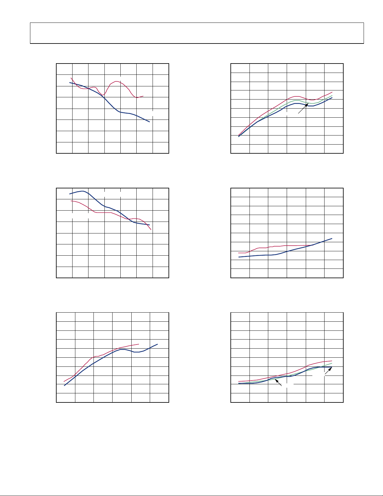
Figure 49. AD9736 SFDR vs. f
90
85
80
THIRD-ORDER IMD_2×
75
70
65
SFDR, IMD (dBc)
60
55
50
Figure 50. AD9736 IMD vs. f
–150
–152
–154
–156
–158
–160
–162
NSD (dBm/Hz)
–164
–166
–168
–170
Figure 51. AD9736 1-Tone NSD vs. f
SFDR_2×
SFDR_1×
f
(MHz)
OUT
, 25°C, 1.2 GSPS, 1× and 2× Interpolation
OUT
THIRD-ORDER IMD_1×
f
(MHz)
OUT
, 25°C, 1.2 GSPS, 1× and 2× Interpolation
OUT
1GSPS
1.2GSPS
f
(MHz)
OUT
over f
DAC
, 25°C
OUT
3500 50 100 150 200 250 300
04862-049
3500 50 100 150 200 250 300
04862-050
6000 100 200 300 400 500
04862-051
–150
–152
–154
–156
–158
–160
–162
NSD (dBm/Hz)
–164
–166
–168
–170
Figure 52. AD9736 1-Tone NSD vs. f
–150
–152
–154
–156
–158
–160
–162
NSD (dBm/Hz)
–164
–166
–168
–170
1GSPS
Figure 53. AD9736 8-Tone NSD vs. f
–150
–152
–154
–156
–158
–160
–162
NSD (dBm/Hz)
–164
–166
–168
–170
Figure 54. AD9736 8-Tone NSD vs. f
f
f
f
+85°C
+25°C
(MHz)
OUT
over Temperature, 1.2 GSPS
OUT
1.2GSPS
(MHz)
OUT
over f
OUT
+85°C
+25°C
(MHz)
OUT
over Temperature, 1.2 GSPS
OUT
–40°C
DAC
–40°C
6000 100 200 300 400 500
04862-052
6000 100 200 300 400 500
04862-053
, 25°C
6000 100 200 300 400 500
04862-054
Rev. 0 | Page 21 of 68
 Loading...