Analog Devices AD9731 b Datasheet

10-Bit, 170 MSPS
a
FEATURES
170 MSPS Update Rate
TTL/High Speed CMOS-Compatible Inputs
Wideband SFDR: 66 dB @ 2 MHz/50 dB @ 65 MHz
Pin-Compatible, Lower Cost Replacement for
Industry Standard AD9721 DAC
Low Power: 439 mW @ 170 MSPS
Fast Settling: 3.8 ns to 1/2 LSB
Internal Reference
Two Package Styles: 28-Lead SOIC and SSOP
APPLICATIONS
Digital Communications
Direct Digital Synthesis
Waveform Reconstruction
High Speed Imaging
5 MHz to 65 MHz HFC Upstream Path
CLOCK
D/A Converter
AD9731
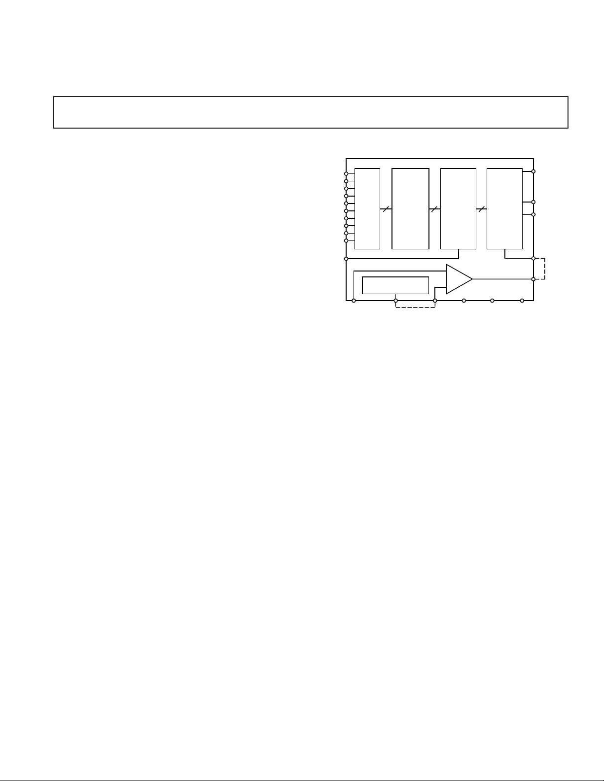
FUNCTIONAL BLOCK DIAGRAM
ANALOG
–V
S
ANALOG
RETURN
IOUT
IOUT
REF IN
AMP OUT
D9
D8
D7
D6
TTL
D5
DRIVE
D4
LOGIC
D3
D2
D1
D0
R
SET
DECODERS
AND
DRIVERS
INTERNAL VOLTAGE
REFERENCE
REF OUT CONTROL
AMP IN
REGISTER
CONTROL
AMP
DIGITAL
–V
S
SWITCH
NETWORK
DIGITAL
+V
S
GENERAL DESCRIPTION
The AD9731 is a 10-bit, 170 MSPS, bipolar D/A converter that is
optimized to provide high dynamic performance, yet offer lower
power dissipation and more economical pricing than afforded by
previous bipolar high performance DAC solutions. The AD9731
was designed primarily for demanding communications systems
applications where wideband spurious-free dynamic range (SFDR)
requirements are strenuous and could previously only be met by
using a high performance DAC such as the industry-standard
AD9721. The proliferation of digital communications into base
station and high volume subscriber-end markets has created a
demand for excellent DAC performance delivered at reduced
levels of power dissipation and cost. The AD9731 is the answer
to that demand.
REV. B
Optimized for direct digital synthesis (DDS) waveform reconstruction, the AD9731 provides 50 dB of wideband harmonic
suppression over a dc-to-65 MHz analog output bandwidth.
This signal bandwidth addresses the transmit spectrum in many
of the emerging digital communications applications where
signal purity is critical. Narrowband, the AD9731 provides an
SFDR of greater than 79 dB. This excellent wideband and
narrowband ac performance, coupled with a lower pricing structure,
make the AD9731 the optimum high performance DAC value.
The AD9731 is packaged in 28-lead SOIC (same footprint
as the industry-standard AD9721) and super space-saving
28-lead SSOP; both are specified to operate over the extended
industrial temperature range of –40∞C to +85∞C.
Information furnished by Analog Devices is believed to be accurate and
reliable. However, no responsibility is assumed by Analog Devices for its
use, nor for any infringements of patents or other rights of third parties that
may result from its use. No license is granted by implication or otherwise
under any patent or patent rights of Analog Devices. Trademarks and
registered trademarks are the property of their respective companies.
One Technology Way, P.O. Box 9106, Norwood, MA 02062-9106, U.S.A.
Tel: 781/329-4700 www.analog.com
Fax: 781/326-8703 © 2003 Analog Devices, Inc. All rights reserved.

AD9731–SPECIFICATIONS
(+VS = +5 V, –VS = –5.2 V, CLOCK = 125 MHz, R
V
= –1.25 V, unless otherwise noted.)
REF
= 1.96 k⍀ for 20.4 mA I
SET
OUT
,
Test
Parameter Temp Level Min Typ Max Unit
RESOLUTION 10 Bits
MAX CONVERSION RATE –40∞C to +85∞CIV 170 MHz
DC ACCURACY
Differential Nonlinearity 25∞CI 0.25 1 LSB
Full VI 0.35 1.5 LSB
Integral Nonlinearity 25∞CI 0.6 1 LSB
Full VI 0.7 1.5 LSB
INITIAL OFFSET ERROR
Zero-Scale Offset Error 25∞CI 3570 mA
Full VI 40 100 mA
25∞CI 2.5 5 % FS
Full-Scale Gain Error
1
Full VI 2.5 5 % FS
Offset Drift Coefficient V 0.04 mA/∞C
REFERENCE/CONTROL AMP
Internal Reference Voltage
Internal Reference Voltage Drift Full IV 100 mV/∞C
Internal Reference Output Current
2
3
25∞CI–1.35 –1.25 –1.15 V
Full VI –50 +500 mA
Amplifier Input Impedance 25∞CV 50 kW
Amplifier Bandwidth 25∞CV 2.5 MHz
4, 6
4
5
25∞CV 75 MHz
25∞CV 20 mA
REFERENCE INPUT
Reference Input Impedance 25∞CV 4.6 kW
Reference Multiplying Bandwidth
OUTPUT PERFORMANCE
Output Current
Output Compliance 25∞CIV–1.5 +3 V
Output Resistance 25∞CV 240 W
Output Capacitance 25∞CV 5 pF
Voltage Settling Time to 1/2 LSB (t
Propagation Delay (t
Glitch Impulse
9
Output Slew Rate
Output Rise Time
Output Fall Time
8
)
PD
10
10
10
ST
7
)
25∞CV 3.8 ns
25∞CV 2.9 ns
25∞CV 4.1 pVs
25∞CV 400 V/ms
25∞CV 1 ns
25∞CV 1 ns
DIGITAL INPUTS
Input Capacitance Full IV 2 pF
Logic “1” Voltage Full VI 2.0 V
Logic “0” Voltage Full VI 0.8 V
Logic “1” Current 25∞CVI 850mA
Logic “0” Current 25∞CVI 30100 mA
Data Setup Time (t
Data Hold Time (t
11
)
S
12
)
H
25∞CIV2 ns
Full IV 2.5 ns
25∞CIV1.0 0.1 ns
Full IV 1.0 0.1 ns
Clock Pulsewidth Low (pw
Clock Pulsewidth High (pw
SFDR PERFORMANCE (Wideband)
A
= 0 dBFS
OUT
2 MHz f
10 MHz f
20 MHz f
40 MHz f
65 MHz f
70 MHz f
OUT
OUT
OUT
OUT
(Clock = 170 MHz) 25∞CV 50 dB
OUT
(Clock = 170 MHz) 25∞CV 47 dB
OUT
)25∞CIV2 ns
MIN
)25∞CIV2 ns
MAX
13
25∞CV 66 dB
25∞CV 62 dB
25∞CV 61 dB
25∞CV 55 dB
–2–
REV. B

AD9731
SPECIFICATIONS
Test
Parameter Temp Level Min Typ Max Unit
SFDR PERFORMANCE (Narrowband)
2 MHz; 2 MHz Span 25∞CV 79 dB
25 MHz, 2 MHz Span 25∞CV 61 dB
10 MHz, 5 MHz Span (Clock = 170 MHz) 25∞CV 73 dB
INTERMODULATION DISTORTION
F1 = 800 kHz, F2 = 900 kHz 25∞CV 58 dB
POWER SUPPLY
15
Digital –V Supply Current 25∞CI 2737 mA
Analog –V Supply Current 25∞CI 4553 mA
Digital +V Supply Current 25∞CI 1320 mA
Power Dissipation 25∞CV 439 mW
PSRR 25∞CV 100 mA/V
NOTES
1
Measured as an error in ratio of full-scale current to current through R
2
Internal reference voltage is tested under load conditions specified in Internal Reference Output current specification.
3
Internal reference output current defines load conditions applied during Internal Reference Voltage test.
4
Full-scale current variations among devices are higher when driving REFERENCE IN directly.
5
Frequency at which a 3 dB change in output of DAC is observed; RL = 50 W; 100 mV modulation at midscale.
6
Based on IFS = 32 (CONTROL AMP IN/R
7
Measured as voltage settling at midscale transition to ± 0.5 LSB, RL = 50 W.
8
Measured from 50% point of rising edge of CLOCK signal to 1/2 LSB change in output signal.
9
Peak glitch impulse is measured as the largest area under a single positive or negative transient.
10
Measured with RL = 50 W and DAC operating in latched mode.
11
Data must remain stable for specified time prior to rising edge of CLOCK.
12
Data must remain stable for specified time after rising edge of CLOCK.
13
SFDR is defined as the difference in signal energy between the full-scale fundamental signal and worst-case spurious frequencies in the output spectrum window.
The frequency span is dc-to-Nyquist unless otherwise noted.
14
Intermodulation distortion is the measure of the sum and difference products produced when a two-tone input is driven into the DAC. The distortion products
created will manifest themselves at (2F2–F1) and (2F1–F2) of the two tones.
15
Supply voltages should remain stable within ± 5% for nominal operation.
Specifications subject to change without notice.
13
14
Full VI 27 42 mA
Full VI 45 66 mA
Full VI 15 22 mA
Full V 449 mW
(640 mA nominal); ratio is nominally 32. DAC load is virtual ground.
SET
) when using internal control amplifier. DAC load is virtual ground.
SET
pw
MIN
pw
MAX
REV. B
CLOCK
DATA
ANALOG OUTPUT
ANALOG OUTPUT
t
S
CODE 1
DATA
CODE 1
DETAIL OF SETTLING TIME
CLOCK
t
PD
t
ST
t
H
CODE 2
DATA
CODE 2
SPECIFIED
ERROR BAND
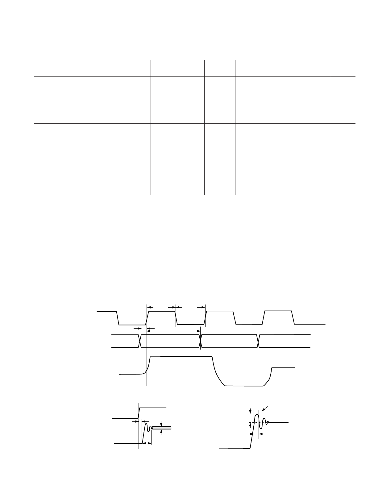
Figure 1. Timing Diagrams
–3–
CODE 3
DATA
CODE 3
CODE 4
CODE 4
GLITCH AREA =
1/2 HEIGHT ⴛ WIDTH
H
W
DATA

AD9731
ABSOLUTE MAXIMUM RATINGS*
Analog Output . . . . . . . . . . . . . . . . . . . . . . . . . . . . –VS to +V
S
+VS . . . . . . . . . . . . . . . . . . . . . . . . . . . . . . . . . . . . . . . . +6 V
Digital Inputs . . . . . . . . . . . . . . . . . . . . . . . . . –0.7 V to +V
S
–VS . . . . . . . . . . . . . . . . . . . . . . . . . . . . . . . . . . . . . . . . . –7 V
Analog Output Current . . . . . . . . . . . . . . . . . . . . . . . . 30 mA
Control Amplifier Input Voltage Range . . . . . . . . 0 V to –4 V
Reference Input Voltage Range . . . . . . . . . . . . . . . 0 V to –V
S
Maximum Junction Temperature . . . . . . . . . . . . . . . . 150∞C
Operating Temperature Range . . . . . . . . . . . –40∞C to +85∞C
Internal Reference Output Current . . . . . . . . . . . . . . . 500 mA
Lead Temperature (10 sec Soldering) . . . . . . . . . . . . . 300∞C
Storage Temperature . . . . . . . . . . . . . . . . . . –65∞C to +165∞C
Control Amplifier Output Current . . . . . . . . . . . . . ± 2.5 mA
*Stresses above those listed under Absolute Maximum Ratings may cause perma-
nent damage to the device. This is a stress rating only; functional operation of the
device at these or any other conditions above those indicated in the operational
sections of this specification is not implied. Exposure to absolute maximum rating
conditions for extended periods may affect device reliability.
ORDERING GUIDE
Temperature Package Package
Model Range Description Options
AD9731BR –40∞C to +85∞C 28-Lead Wide Body (SOIC) R-28
AD9731BR-REEL –40∞C to +85∞C 28-Lead Wide Body (SOIC) R-28
AD9731BRS –40∞C to +85∞C 28-Lead Shrink Small (SSOP) RS-28
AD9731BRS-REEL –40∞C to +85∞C 28-Lead Shrink Small (SSOP) RS-28
AD9731-PCB 0∞C to 70∞C PCB
EXPLANATION OF TEST LEVELS
Test Level Definition
I 100% production tested
II The parameter is 100% production tested at
25∞C; sampled at temperature production.
III Sample tested only
IV Parameter is guaranteed by design and
characterization testing.
V Parameter is a typical value only.
VI All devices are 100% production tested at 25∞C;
guaranteed by design and characterization testing
for industrial temperature range devices.
CAUTION
ESD (electrostatic discharge) sensitive device. Electrostatic charges as high as 4000 V readily
accumulate on the human body and test equipment and can discharge without detection. Although
the AD9731 features proprietary ESD protection circuitry, permanent damage may occur on
devices subjected to high energy electrostatic discharges. Therefore, proper ESD precautions are
recommended to avoid performance degradation or loss of functionality.
–4–
REV. B
 Loading...