16-Bit, 400 MSPS
FEATURES
Dynamic performance
SFDR ≥ 78 dBc @ f
IMD ≥ 82 dBc @ f
ACLR ≥ 76 dBc @ f
NSD ≤ –160 dB/Hz @ f
Precision calibrated linearity
DNL ≤ ±0.5 LSB @ +25°C
INL ≤ ±1.0 LSB @ +25°C
THD ≤ –95 dB @ f
LVDS inputs with internal 100 Ω terminations
Automatic data/clock timing synchronization
Single data rate or double data rate capable
Differential current outputs
Internal precision reference
Operates on 2.5 V and 3.3 V supplies
Extended industrial temperature range
Thermally enhanced, 80-lead, lead-free TQFP_EP package
APPLICATIONS
Instrumentation
Test equipment
Waveform synthesis
Communications systems
GENERAL DESCRIPTION
The AD9726 is a 16-bit digital-to-analog converter (DAC)
that offers leading edge performance at conversion rates up to
400 MSPS. The device uses low voltage differential signaling
(LVDS) inputs and includes internal 100 Ω terminations. The
analog output can be single-ended or differential current. An
internal precision reference is included.
The AD9726 also features synchronization logic to monitor and
optimizes the timing between incoming data and the sample clock.
This reduces system complexity and simplifies timing requirements. An LVDS clock output is also available to drive an external
data pump in either single data rate (SDR) or double data rate
(DDR) mode.
All device operation is fully programmable using the flexible
serial port interface (SPI). The AD9726 is also fully functional
in its default state for applications without a controller.
= 20 MHz
OUT
= 70 MHz
OUT
= 70 MHz
OUT
OUT
= 1 MHz
OUT
= 70 MHz
D/A Converter
AD9726
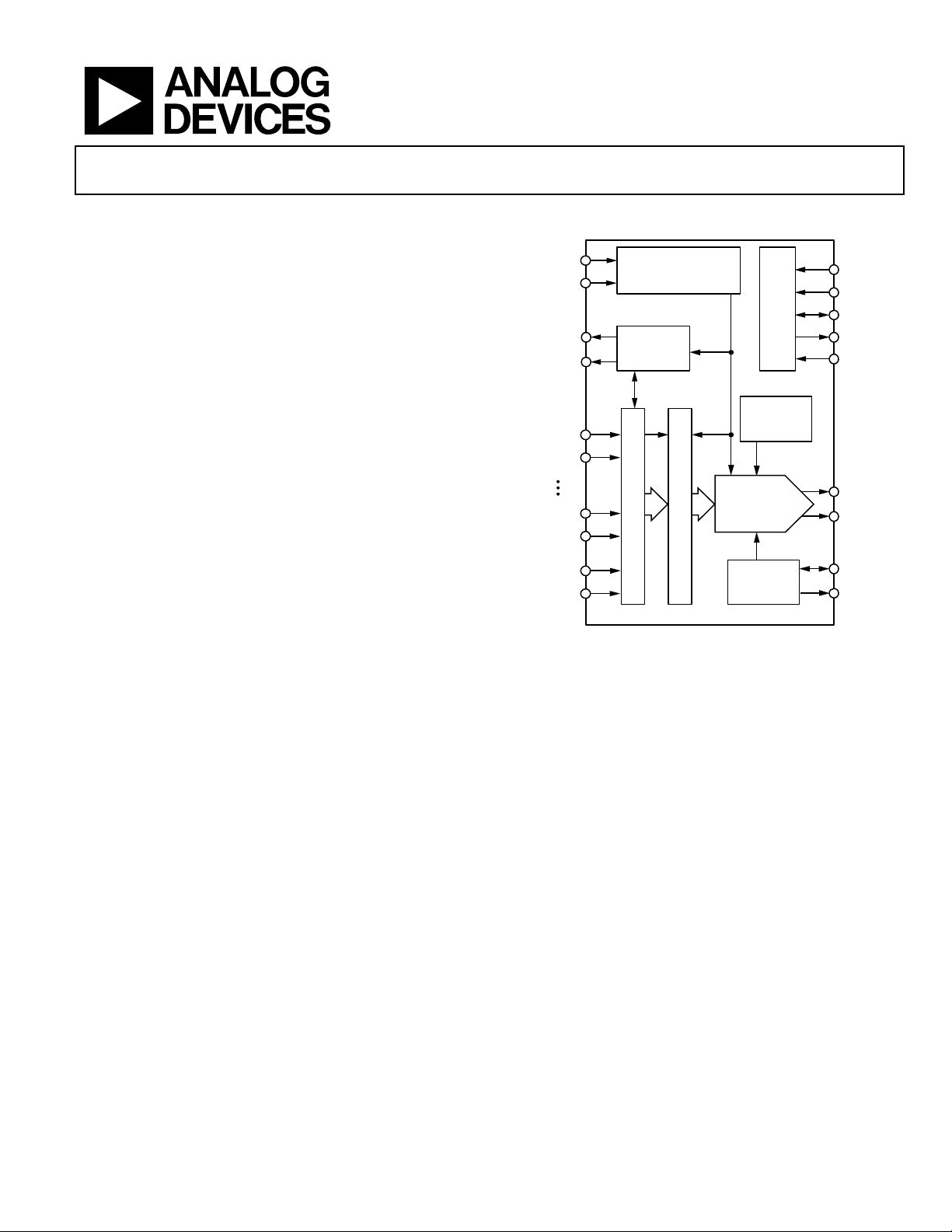
FUNCTIONAL BLOCK DIAGRAM
CLK+
CLK–
DCLK_OUT+
DCLK_OUT–
DB[15]+
DB[15]–
DB[0]+
DB[0]–
DCLK_IN+
DCLK_IN–
PRODUCT HIGHLIGHTS
1. A unique combination of precision and performance
makes the AD9726 equally suited to applications with
demanding frequency domain or demanding time domain
requirements.
2. Nonvolatile factory calibration assures a highly linear
transfer function. Internal logic offers on demand selfcalibration for linearity even at extended operating
temperatures.
3. Proprietary architecture minimizes data dependent,
discrete mixing spurs and offers enhanced dynamic
performance over a wide range of output frequencies.
High input data rates create a very high frequency
synthesis bandwidth.
4. The fully automatic, transparent synchronizer maintains
optimized timing between clock and data in real time and
offers programmable control options for added flexibility.
5. Full-scale output current is external resistor programmable.
CLOCK DISTRIBUTION
AND CONTROL
LVDS OUTPUT
DRIVER
LVDS INPUT DATA CAPTURE
DATA SYNCHRONIZATION
Figure 1.
.
SPI
CALIBRATION
MEMORY
16-BIT
DAC
INTERNAL
REFERENCE
CSB
SCLK
SDIO
SDO
RESET
I
OUTA
I
OUTB
REFIO
FSADJ
04540-001
Rev. A
Information furnished by Analog Devices is believed to be accurate and reliable. However, no
responsibility is assumed by Anal og Devices for its use, nor for any infringements of patents or other
rights of third parties that may result from its use. Specifications subject to change without notice. No
license is granted by implication or otherwise under any patent or patent rights of Analog Devices.
Trademarks and registered trademarks are the property of their respective owners.
One Technology Way, P.O. Box 9106, Norwood, MA 02062-9106, U.S.A.
Tel: 781.329.4700
Fax: 781.461.3113 © 2005 Analog Devices, Inc. All rights reserved.
www.analog.com

AD9726
TABLE OF CONTENTS
Features .............................................................................................. 1
Applications....................................................................................... 1
Functional Block Diagram .............................................................. 1
General Description......................................................................... 1
Product Highlights........................................................................... 1
Specifications..................................................................................... 3
DC Specifications ......................................................................... 3
AC Specifications.......................................................................... 4
Digital Signal Specifications........................................................ 5
Timing Specifications .................................................................. 5
Timing Diagrams.......................................................................... 6
Absolute Maximum Ratings............................................................ 7
Thermal Resistance ...................................................................... 7
ESD Caution.................................................................................. 7
Pin Configuration and Function Descriptions............................. 8
Serial Port Interface........................................................................ 13
Theory of Operation ...................................................................... 15
DAC Clock and Data Clock Output........................................ 15
Data Clock Input........................................................................ 15
Data Synchronization Circuitry............................................... 16
Analog Output............................................................................ 16
Internal Reference and Full-Scale Output .............................. 16
Reset ............................................................................................. 17
Serial Port Interface ................................................................... 17
SPI Pin Description.................................................................... 18
Calibration................................................................................... 18
Sync Logic Operation and Programming ............................... 20
Outline Dimensions ....................................................................... 22
Ordering Guide .......................................................................... 22
Te r mi n ol o g y .................................................................................... 10
Typical Performance Characteristics ........................................... 11
REVISION HISTORY
11/05—Rev. 0 to Rev. A
Changes to Features.......................................................................... 1
Changes to Table 3 and Table 4....................................................... 5
Changes to the Terminology Section........................................... 10
Changes to the Driving the DAC Clock Inputs Section............ 15
Changes to the Reset and Serial Port Interface Sections........... 17
Updated Outline Dimensions....................................................... 22
Changes to the Ordering Guide.................................................... 22
7/05—Revision 0: Initial Version
Rev. A | Page 2 of 24

AD9726
SPECIFICATIONS
DC SPECIFICATIONS
DBVDD = AVDD1 = AVDD2 = 3.3 V, DVDD = CLKVDD = ADVDD = ACVDD = 2.5 V, I
to T
T
MIN
, unless otherwise specified.
MAX
Table 1.
Parameter Min Typ Max Unit
ACCURACY
1
DNL ±0.5 ±1.0 LSB
INL ±1.0 ±2.5 LSB
Offset Error 0.003 % FS
Gain Error 0.003 % FS
ANALOG OUTPUT
Full-Scale Current 20 mA
Compliance Voltage ±1 V
Output Impedance
10
INTERNAL REFERENCE
Output Voltage 1.18 1.22 1.27 V
Output Current
2
1 µA
EXTERNAL REFERENCE
Input Voltage 1.2 V
Input Resistance 10 MΩ
Small Signal Bandwidth 200 kHz
TEMPERATURE COEFFICIENTS
Gain Drift ±10 ppm of FS/ºC
Offset Drift ±10 ppm of FS/ºC
Reference Drift ±30 ppm/ºC
POWER SUPPLIES
3
AVDD1, AVDD2
Voltage Range 3.13 3.47 V
Supply Current (I
AVDD1
+ I
) 52 60 mA
AVDD2
ADVDD, ACVDD
Voltage Range 2.37 2.63 V
Supply Current (I
ACVDD
+ I
) 16 18 mA
ADVDD
CLKVDD
Voltage Range 2.37 2.63 V
Supply Current (I
) 45 50 mA
CLKVDD
DVDD
Voltage Range 2.37 2.63 V
Supply Current (I
) 80 90 mA
DVDD
DBVDD
Voltage Range 3.13 3.47 V
Supply Current (I
POWER DISSIPATION (P
) 16 18 mA
DBVDD
) 575 mW
DISS
Sleep Mode 465 mW
Power-Down Mode ≤10 mW
OPERATING TEMPERATURE RANGE –40 +85 °C
1
T
= 25°C.
AMB
2
Use buffer amplifier to drive external load.
3
Supply currents and power dissipation measured in SDR with f
= 400 MHz and f
DAC
= 1 MHz.
OUT
= 20 mA, internal reference,
OUT-FS
MΩ
Rev. A | Page 3 of 24

AD9726
AC SPECIFICATIONS
DBVDD = AVDD1 = AVDD2 = 3.3 V, DVDD = CLKVDD = ADVDD = ACVDD = 2.5 V, I
to T
T
MIN
, unless otherwise specified.
MAX
Table 2.
Parameter Min Typ Max Unit
TOTAL HARMONIC DISTORTION (THD)
f
= 400 MHz, f
DAC
= 1 MHz, 0 dBFS –95 dB
OUT
SPURIOUS-FREE DYNAMIC RANGE (SFDR)
f
= 400 MHz, 0 dBFS
DAC
f
= 20 MHz 78 dBc
OUT
f
= 70 MHz 68 dBc
OUT
f
= 140 MHz 62 dBc
OUT
f
= 400 MHz, –3 dBFS
DAC
f
= 20 MHz 80 dBc
OUT
f
= 70 MHz 70 dBc
OUT
f
= 140 MHz 62 dBc
OUT
f
= 200 MHz, 0 dBFS
DAC
f
= 20 MHz 84 dBc
OUT
f
= 70 MHz 62 dBc
OUT
f
= 200 MHz, –3 dBFS
DAC
f
= 20 MHz 82 dBc
OUT
f
= 70 MHz 68 dBc
OUT
TWO-TONE INTERMODULATION DISTORTION (IMD)
f
= 400 MHz, 0 dBFS
DAC
f
= 20 MHz, f
OUT1
f
= 70 MHz, f
OUT1
f
= 140 MHz, f
OUT1
= 21 MHz 86 dBc
OUT2
= 71 MHz 82 dBc
OUT2
= 141 MHz 74 dBc
OUT2
ADJACENT CHANNEL LEAKAGE RATIO (ACLR)
f
= 245.76 MSPS, f
DATA
f
= 245.76 MSPS, f
DATA
f
= 245.76 MSPS, f
DATA
f
= 245.76 MSPS, f
DATA
= 70 MHz, 1-Carrier WCDMA 76 dBc
CARRIER
= 70 MHz, 2-Carrier WCDMA 70 dBc
CARRIER
= 70 MHz, 4-Carrier WCDMA 66 dBc
CARRIER1
= 70 MHz, 8-Carrier WCDMA 62 dBc
CARRIER1
NOISE SPECTRAL DENSITY (NSD)
f
= 400 MHz, f
DAC
f
= 400 MHz, f
DAC
f
= 400 MHz, f
DAC
= 70 MHz, 0 dBFS –160 dBm/Hz
OUT
= 70 MHz, –3 dBFS –163 dBm/Hz
OUT
= 70 MHz, –6 dBFS –165 dBm/Hz
OUT
UPDATE RATE 0 400 MSPS
= 20 mA, internal reference,
OUT-FS
Rev. A | Page 4 of 24

AD9726
DIGITAL SIGNAL SPECIFICATIONS
DBVDD = AVDD1 = AVDD2 = 3.3 V, DVDD = CLKVDD = ADVDD = ACVDD = 2.5 V, I
to T
T
MIN
, unless otherwise specified.
MAX
Table 3.
Parameter Min Typ Max Unit
DAC CLOCK INPUTS (CLK+/–)
Differential Voltage 0.5 1.0 V
Common-Mode Voltage 1.0 1.25 V
LVDS INPUTS (DB[15:0]+/–, DCLK_IN+/–)
Input Voltage Range 825 1575 mV
Differential Threshold Voltage 100 mV
Differential Input Impedance 100 Ω
LVDS OUTPUT (DCLK_OUT+/–)
Differential Output Voltage
1
250 400 mV
Offset Voltage 1.0 1.2 V
Short-Circuit Output Current 20 mA
CMOS INPUTS (CSB, SCLK, SDIO, RESET)
Logic 0 Voltage 0.5 V
Logic 1 Voltage 2.5 V
Input Current 1 nA
CMOS OUTPUTS (SDO, SDIO)
Logic 0 Voltage 0.5 V
Logic 1 Voltage 3.0 V
Short-Circuit Output Current 10 mA
CONTROL INPUTS (SPI_DIS, SDR_EN)
Logic 0 Voltage 0.5 V
Logic 1 Voltage 2.0 V
Input Current 1 nA
1
With 100 Ω external load.
= 20 mA, internal reference,
OUT-FS
TIMING SPECIFICATIONS
DBVDD = AVDD1 = AVDD2 = 3.3 V, DVDD = CLKVDD = ADVDD = ACVDD = 2.5 V, I
to T
T
MIN
, unless otherwise specified.
MAX
Table 4.
Parameter Min Typ Max Unit
LVDS DATA BUS
DDR DCLK_OUT+/– Propagation Delay (t
DDR DB[15:0]+/– Set-Up Time (t
DDR DB[15:0]+/– Hold Time (t
) –100 ps
DSU-DDR
) 500 ps
DH-DDR
SDR DCLK_OUT+/– Propagation Delay (t
SDR DB[15:0]+/– Set-Up Time (t
SDR DB[15:0]+/– Hold Time (t
) –100 ps
DSU-SDR
) 500 ps
DH-SDR
) 2000 ps
DCPD-DDR
) 300 ps
DCPD-SDR
SERIAL PORT INTERFACE
SCLK Frequency (f
) 15 MHz
SCLK
SCLK Rise/Fall Time 1 ms
SCLK Pulse Width High (t
SCLK Pulse Width Low (t
SCLK Set-Up Time (t
SDIO Set-Up Time (t
CSU
DSU
) 30 ns
CPWH
) 30 ns
CPWL
) 30 ns
) 30 ns
SDIO Hold Time (tDH) 0 ns
SDIO/SDO Valid Time (tDV) 30 ns
RESET PULSE WIDTH 1.5 ns
Rev. A | Page 5 of 24
= 20 mA, internal reference,
OUT-FS

AD9726
T
T
S
TIMING DIAGRAMS
DAC CLOCK
t
DCPD-DDR
DATACLOCK OUTPU
DATA BUS
DATACLOCK INPUT
DAC CLOCK
DATACLOCK OUTPU
DATA BUS
DATACLOCK INPUT
CSB
SCLK
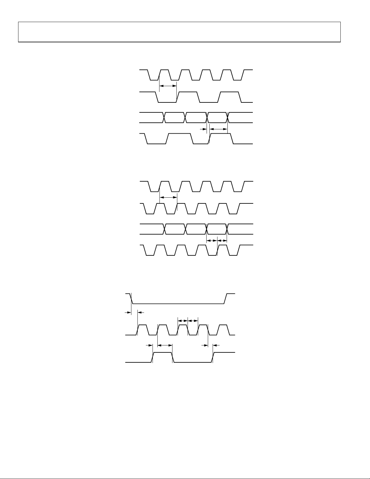
Figure 2. DDR Timing Diagram
t
DCPD-SDR
Figure 3. SDR Timing Diagram
SCLK SET-UP TIME
t
CSU
SCLK PULSE WIDTH HIGH/LOW TIME
t
CPWH
t
DSU-DDR
t
DSU-SDR
t
CPWL
t
DH-DDR
t
DH-SDR
04540-002
04540-003
SDIO SET-UP TIME SDIO HOLD TIME SDIO (SD0) VALID TIME
DIO (SD0)
t
DSU
t
DH
t
DV
04540-004
Figure 4. SPI Timing Diagram
Rev. A | Page 6 of 24

AD9726
ABSOLUTE MAXIMUM RATINGS
Table 5.
Parameter With Respect to Rating
DBVDD, AVDD1, AVDD2 DBGND, AGND1,
DVDD, CLKVDD,
ACVDD, ADVDD
DBGND, AGND1,
AGND2
DGND, CLKGND,
ACGND, ADGND
REFIO, FSDAJ AGND1 –0.3 V to AVDD1
IOUTA, IOUTB AGND1 –1.0 V to AVDD1
CLK+, CLK– CLKGND –0.3 V to
DB[15:0]+/–,
DCLK_IN+/–,
DCLK_OUT+/–
CSB, SCLK, SDIO,
SDO, RESET, REXT
SDR_EN, SPI_DIS ADGND –0.3 V to
AGND2
DGND, CLKGND,
ACGND, ADGND
DBGND, AGND1,
AGND2
DGND, CLKGND,
ACGND, ADGND
DBGND −0.3 V to
DBGND –0.3 V to DBVDD
–0.3 V to 3.6 V
–0.3 V to 2.8 V
–0.3 V to +0.3 V
–0.3 V to +0.3 V
+ 0.3 V
+ 0.3 V
CLKVDD + 0.3 V
DBVDD + 0.3 V
+ 0.3 V
ADVDD + 0.3 V
Stresses above those listed under Absolute Maximum Ratings
may cause permanent damage to the device. This is a stress
rating only; functional operation of the device at these or any
other conditions above those indicated in the operational
section of this specification is not implied. Exposure to absolute
maximum rating conditions for extended periods may affect
device reliability.
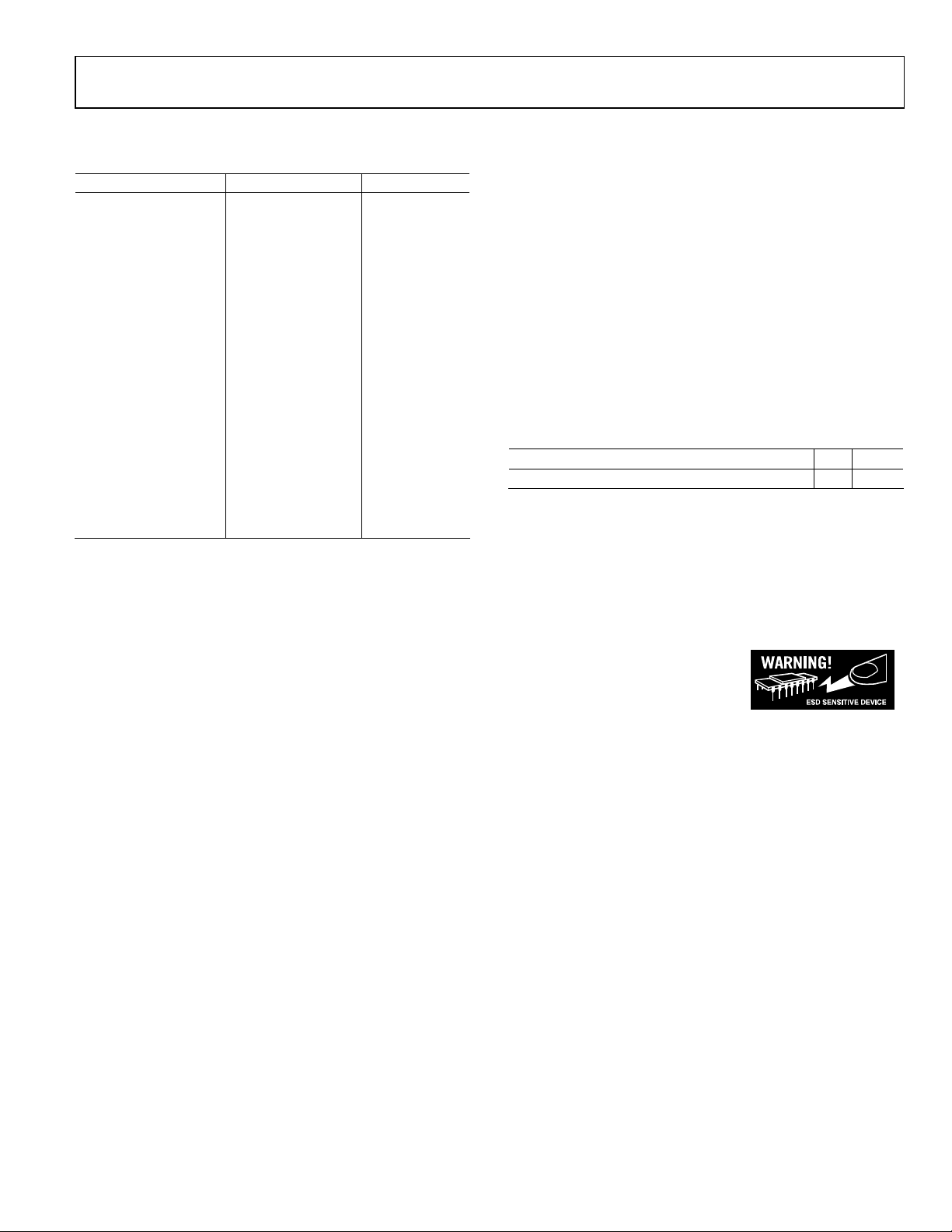
THERMAL RESISTANCE
Thermal impedance can be lowered to 23°C/W by soldering the
exposed package pad to an external heat sink (for example, the
internal PCB copper ground plane). However, this is not necessary
for the power dissipation and operating temperature range of
the AD9726.
Table 6. Thermal Resistance
Package Type θJAUnit
80-Lead TQFP_EP Package, Thermally Enhanced 32 °C/W
ESD CAUTION
ESD (electrostatic discharge) sensitive device. Electrostatic charges as high as 4000 V readily accumulate on the
human body and test equipment and can discharge without detection. Although this product features
proprietary ESD protection circuitry, permanent damage may occur on devices subjected to high energy
electrostatic discharges. Therefore, proper ESD precautions are recommended to avoid performance degradation or loss of functionality.
Rev. A | Page 7 of 24

AD9726
PIN CONFIGURATION AND FUNCTION DESCRIPTIONS
SPI_DIS79ADVDD78ADGND77ACVDD76ACGND75AVDD274AGND273AVDD172AGND171IOUTA70IOUTB69AGND168AVDD167AGND266AVDD265ACGND64ACVDD63ADGND62ADVDD61SDR_EN
80
REXT
CLK+
CLK–
DGND
DVDD
DB15+
DB15–
DB14+
DB14–
DB13+
DB13–
DB12+
DB12–
DB11+
DB11–
DBVDD
1
PIN 1
2
3
4
5
6
7
8
9
10
11
12
13
14
15
16
17
18
19
20
21
22
23
24
25
26
27
28
DB9–
DB8–
DB9+
DB10+
DBGND
DB10–
DB8+
CLKVDD
CLKVDD
CLKGND
CLKGND
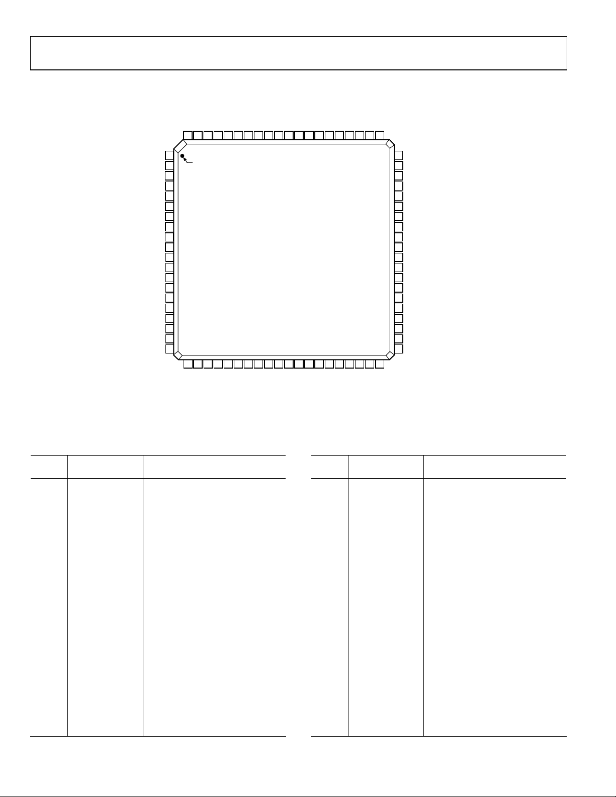
Figure 5. Pin Configuration
Table 7. Pin Function Descriptions
Pin
No. Mnemonic Description
1 CLKVDD Clock Supply Voltage
2 REXT Sets Data Clock Output Drive
3 CLKVDD Clock Supply Voltage
4 CLKGND Clock Supply Common
5 CLK+ DAC Clock Input True
6 CLK− DAC Clock Input Complement
7 CLKGND Clock Supply Common
8 DGND Digital Supply Common
9 DVDD Digital Supply Voltage
10 DB15+ Data Bit 15 True
11 DB15− Data Bit 15 Complement
12 DB14+ Data Bit 14 True
13 DB14− Data Bit 14 Complement
14 DB13+ Data Bit 13 True
15 DB13− Data Bit 13 Complement
16 DB12+ Data Bit 12 True
17 DB12− Data Bit 12 Complement
18 DB11+ Data Bit 11 True
19 DB11− Data Bit 11 Complement
20 DBVDD Data Bus Supply Voltage
21 DBGND Data Bus Supply Common
AD9726
TOP VIEW
(Not to Scale)
29
30
DBVDD
DCLK_OUT–
DCLK_OUT+
1
31
DBGND
60
FSADJ
59
REFIO
58
RESET
57
CSB
56
SCLK (SYNCUPD)
55
SDIO
54
SDO (SYNCALRM)
53
DGND
52
DVDD
51
DB0–
50
DB0+
49
DB1–
48
DB1+
47
DB2–
46
DB2+
45
DB3–
44
DB3+
43
DB4–
42
DB4+
41
DBGND
32
33
34
35
36
37
38
39
40
DB7–
DB6–
DB5–
DB5+
DBVDD
04540-005
DCLK_IN+
DCLK_IN–
DB7+
DB6+
Pin
No. Mnemonic Description
22 DB10+ Data Bit 10 True
23 DB10− Data Bit 10 Complement
24 DB9+ Data Bit 9 True
25 DB9− Data Bit 9 Complement
26 DB8+ Data Bit 8 True
27 DB8− Data Bit 8 Complement
28 DCLK_OUT+ Data Clock Output True
29 DCLK_OUT− Data Clock Output Complement
30 DBVDD Data Bus Supply Voltage
31 DBGND Data Bus Supply Common
32 DCLK_IN+ Data Clock Input True
33 DCLK_IN− Data Clock Input Complement
34 DB7+ Data Bit 7 True
35 DB7− Data Bit 7 Complement
36 DB6+ Data Bit 6 True
37 DB6− Data Bit 6 Complement
38 DB5+ Data Bit 5 True
39 DB5− Data Bit 5 Complement
40 DBVDD Data Bus Supply Voltage
41 DBGND Data Bus Supply Common
42 DB4+ Data Bit 4 True
Rev. A | Page 8 of 24
 Loading...