14-Bit, 600+ MSPS
Preliminary Technical Data
FEATURES
600+ MSPS DAC update rate
16/14/12/10-bit resolution family
LVDS interface with built-in 100-termination resistors
Single data rate and double data rate capability
Excellent dynamic performance
SFDR = 63 dBc at 140 MHz
IMD = 73 dBc at 140 MHz
Differential current outputs: 2 mA to 20 mA
–40°C to +85°C temperature range operation
On-chip 1.20 V reference
Package: 80-lead thermally-enhanced TQFP
Versatile clock and data interface
APPLICATIONS
Instrumentation and test
Wideband communications systems
Point-to-point wireless
LMDS
PA linearization
High resolution displays
PRODUCT DESCRIPTION
The AD9725 is a 14-bit digital-to-analog converter (DAC) that
utilizes an LVDS interface to achieve conversion rates in excess
of 600 MSPS. It is in a family of pin compatible converters that
offers selection of 10-bit, 12-bit, 14-bit, and 16-bit resolution
grades. All of the devices share the same interface options, small
outline package, and pinout, providing an upward or downward
component selection path based on performance, resolution
and cost.
D/A Converter
AD9725
FUNCTIONAL BLOCK DIAGRAM
CALIBRATION REFERENCE
DB[13:0]+
DB[13:0]–
DDR
DATACLK_IN+
DATACLK_IN–
REXT
DATACLK_OUT+
DATACLK_OUT–
CLK+
CLK–
DATA
FORMATTER
DATA CLOCK
FORMATTER
DATA SYNC.
CLOCK DISTRIBUTIO N
AND CONTROL
14-BIT
DAC
SPI
Figure 1
PRODUCT HIGHLIGHTS
Ultralow noise and intermodulation distortion (IMD) enable
high quality waveform synthesis at intermediate frequencies up
to 200 MHz.
LVDS receivers support SDR or DDR modes, with the maximum conversion rate exceeding 600 MSPS.
Manufactured on a CMOS process, the AD9725 uses a proprietary switching technique that enhances dynamic performance.
The current output of the AD9725 can be easily configured for
various single-ended or differential circuit topologies.
FSADJ
REFIO
IOUTA
IOUTB
SDIO
SDO/SYNC _ALRM
CSB
SCLK/SYN C_UPD
RESET
04540-0-001
Rev. PrA
Information furnished by Analog Devices is believed to be accurate and reliable.
However, no responsibility is assumed by Analog Devices for its use, nor for any
infringements of patents or other rights of third parties that may result from its use.
Specifications subject to change without notice. No license is granted by implication
or otherwise under any patent or patent rights of Analog Devices. Trademarks and
registered trademarks are the property of their respective owners.
One Technology Way, P.O. Box 9106, Norwood, MA 02062-9106, U.S.A.
Tel: 781.329.4700 www.analog.com
Fax: 781.326.8703 © 2004 Analog Devices, Inc. All rights reserved.

AD9725
TABLE OF CONTENTS
Preliminary Technical Data
Specifications..................................................................................... 3
DC Specifications ......................................................................... 3
AC Specifications.......................................................................... 4
Digital Specifications ................................................................... 5
Digital Timing Information........................................................ 5
Absolute Maximum Ratings............................................................ 6
Pin Configuration and Function Description .............................. 7
Serial Port Interface Register Maps................................................ 9
Definitions....................................................................................... 11
Typical Performance Curves......................................................... 12
Theory of Operation ...................................................................... 13
LVDS Inputs................................................................................ 13
Data Synchronization Circuitry............................................... 13
Internal Reference and Full-Scale Output Current................ 13
Analog Output............................................................................ 14
SPI Port Control......................................................................... 14
General Operation of the Serial Port Interface ...................... 14
Instruction Byte.......................................................................... 14
Serial Port Interface Pin Description....................................... 14
Notes on Serial Port Operation................................................ 15
Outline Dimension......................................................................... 16
Ordering Guide .......................................................................... 16
Rev. PrA | Page 2 of 16

Preliminary Technical Data
AD9725
SPECIFICATIONS
DC SPECIFICATIONS
Table 1. T
otherwise noted. Specifications subject to change without notice
Parameter Min Typ Max Unit
Resolution 14 Bits
DC Accuracy
Integral Nonlinearity ±1.5 LSB
Differential Nonlinearity ±0.75 LSB
Analog Output
Offset Error –1 1 %FSR
Gain Error %FSR
Full Scale Output Current 20 1.26 mA
Output Compliance Range 1.14 V
Output Resistance TBD 1.25 kW
Output Capacitance 0.1 TBD pF
Reference Output
Reference Voltage 1.2 V
Reference Output Current 100 nA
Reference Input
Reference Input Compliance Range V
Reference Input Resistance 5 kW
Small Signal Bandwidth 0.5 MHz
Temperature Coefficients
Offset Drift TBD ppm of FSR/ºC
Gain Drift (With Internal Reference) TBD ppm of FSR/ºC
Reference Voltage Drift TBD ppm/ºC
Power Supply1
AVDD1, AVDD2
Voltage Range 3.3 V
Analog Supply Current (I
ADVDD
Voltage Range 2.5 V
ACVDD mA
Voltage Range 2.5 V
Analog Supply Current ( I
CLKVDD
Voltage Range 2.5 V
Clock Supply Current (I
DVDD
Voltage Range 2.5 V
Digital Supply Current (I
DBVDD
Voltage Range 3.3 V
Digital Supply Current (I
Nominal Power Dissipation (P
Nominal Power Dissipation (P
1
Supply currents measured under the following conditions: f
2
Power dissipation measured under the following conditions: f
3
Power dissipation measured under the following conditions: f
MIN
to T
, AVDD1, AVDD2, DBVDD = 3.3 V, ADVDD, ACVDD, CLKVDD, DVDD = 2.5 V, I
MAX
+ I
AVDD1
ADVDD
) 20 mA
CLKVDD
) 69 mA
DVDD
DBVDD
) 51 mA
AVDD2
+ I
) 9 mA
ACVDD
) 20 mA
)2 479 mW
DIS
)3 1000 mW
DIS
= 200 MSPS, f
DAC
= 200 MSPS, f
DAC
= 600 MSPS, f
DAC
= 11 MHz, nominal power supply voltages
OUT
= 11 MHz, nominal power supply voltages
OUT
= 111 MHz, nominal power supply voltages
OUT
= 20 mA, unless
OUTFS
Rev. PrA | Page 3 of 16

AD9725
Preliminary Technical Data
AC SPECIFICATIONS
Table 2. T
otherwise noted. Specifications subject to change without notice.
Parameter Typ Unit
Dynamic Performance
Max DAC Output Update Rate (DDR) 600 MSPS
Max DAC Output Update Rate (SDR) 440 MSPS
AC Linearity
Spurious Free Dynamic Range (SFDR) to Nyquist (f
f
f
f
f
f
f
f
f
f
Two Tone IMD to Nyquist (f
f
f
f
f
f
f
f
f
f
Noise Spectral Density (NSD)
f
f
f
f
CDMA2000 Adjacent Channel Leakage Ratio (ACLR)
f
f
f
WCDMA Adjacent Channel Leakage Ratio (ACLR), Single Carrier
f
f
f
f
WCDMA Adjacent Channel Leakage Ratio (ACLR), Four Carrier
f
f
to T
MIN
= 260 MSPS, f
DATA
= 260 MSPS, f
DATA
= 260 MSPS, f
DATA
= 400 MSPS, f
DATA
= 400 MSPS, f
DATA
= 400 MSPS, f
DATA
= 600 MSPS, f
DATA
= 600 MSPS, f
DATA
= 600 MSPS, f
DATA
= 300 MSPS, f
DATA
= 300 MSPS, f
DATA
= 300 MSPS, f
DATA
= 500 MSPS, f
DATA
= 500 MSPS, f
DATA
= 500 MSPS, f
DATA
= 600 MSPS, f
DATA
= 600 MSPS, f
DATA
= 600 MSPS, f
DATA
= 500 MSPS, f
DATA
= 500 MSPS, f
DATA
= 500 MSPS, f
DATA
= 500 MSPS, f
DATA
= 245.76 MSPS, IF = 61.44 MHz TBD dBc
DATA
= 491.52 MSPS, IF = 122.88 MHz TBD dBc
DATA
= 491.52 MSPS, IF = 190 MHz TBD dBc
DATA
= 184.32 MSPS, IF = 61.44 MHz 79 dBc
DATA
= 245.76 MSPS, IF= 61.44 MHz 79 dBc
DATA
= 491.52 MSPS, IF = 122.88 MHz 76 dBc
DATA
= 491.52 MSPS, IF = 190 MHz 74 dBc
DATA
= 184.32 MSPS, IF = 61.44 MHz, 69 dBc
DATA
= 368.64 MSPS, IF = 92.16 MHz 67 dBc
DATA
, AVDD1, AVDD2, DBVDD = 3.3 V, ADVDD, ACVDD, CLKVDD, DVDD = 2.5 V, I
MAZ
= 0 dBFS)
OUT
= 20 MHz 71 dBc
OUT
= 70 MHz 68 dBc
OUT
= 120 MHz 68 dBc
OUT
= 20 MHz 72 dBc
OUT
= 70 MHz 66 dBc
OUT
= 140 MHz 60 dBc
OUT
= 20 MHz TBD dBc
OUT
= 125 MHz TBD dBc
OUT
= 250 MHz TBD dBc
OUT
= f
OUT1
= 26 MHz, f
OUT1
= 100 MHz, f
OUT1
= 126 MHz, f
OUT1
= 26 MHz, f
OUT1
= 100 MHz, f
OUT1
= 126 MHz, f
OUT1
= 26 MHz, f
OUT1
= 126 MHz, f
OUT1
= 250 MHz, f
OUT1
= 20 MHz, 0 dBFS –162 dBm/Hz
OUT
= 20 MHz, –12 dBFS –165 dBm/Hz
OUT
= 120 MHz, 0 dBFS –151 dBm/Hz
OUT
= 120 MHz, –12 dBFS –161 dBm/Hz
OUT
= –6 dBFS)
OUT2
= 27 MHz 89 dBc
OUT2
= 101 MHz 80 dBc
OUT2
= 127 MHz 80 dBc
OUT2
= 27 MHz 90 dBc
OUT2
= 101 MHz 78 dBc
OUT2
= 127 MHz 76 dBc
OUT2
= 27 MHz TBD dBc
OUT2
= 127 MHz TBD dBc
OUT2
= 251 MHz TBD dBc
OUT2
OUTFS
= 20 mA, unless
Rev. PrA | Page 4 of 16

Preliminary Technical Data
T
AD9725
DIGITAL SPECIFICATIONS
Table 3. T
otherwise noted. Specifications subject to change without notice.
Parameter Conditions Min Typ Max Unit
Digital Inputs VCM = 0.875 V to 1.575 V
Differential Logic ‘1’
Differential Logic ‘0’ –0.6 –0.1 V
Logic ‘1’ current 3.5 mA
Logic ‘0’ current 3.5 mA
Differential Input Resistance 100 W
Differential Input Capacitance 3 pF
Data Setup Time (tDS) 0.9 ns
Data Hold Time (tDH) –0.3 ns
Data Clock Output Delay ( t
Serial Control Bus
Maximum SCLK Frequency (fSCLK) 15 MHz
Minimum Clock Pulse Width High (t
Minimum Clock Pulse Width Low (t
Maximum Clock Rise/Fall Time 1 ms
Minimum Data/Chip Select Set Up Time (tDS) 25 ns
Minimum Data Hold Time (tDH) 0 ns
Maximum Data Valid Time (tDV) 30 ns
RESET Pulse Width 1.5 ns
Inputs (SDI, SDIO, SCLK, CSB)
Logic ‘1’ Voltage 2.1 3 V
Logic ‘0’ Voltage 0 0.9 V
Logic ‘1’ Current –10 +10 µA
Logic ‘0’ Current –10 +10 µA
Input Capacitance 5 pF
SDIO Output
Logic ‘1’ Voltage DRVDD–0.6 V
Logic ‘0’ Voltage 0.4 V
Logic ‘1’ Current 30 50 mA
Logic ‘0’ Current 30 50 mA
MIN
to T
, AVDD1, AVDD2, DBVDD = 3.3 V, ADVDD, ACVDD, CLKVDD, DVDD = 2.5 V , I
MAX
(put into footnote, and delete
0.1 0.6 V
column?)
) 2.4 ns
DCO
) 30 ns
PWH
) 30 ns
PWL
= 20 mA, unless
OUTFS
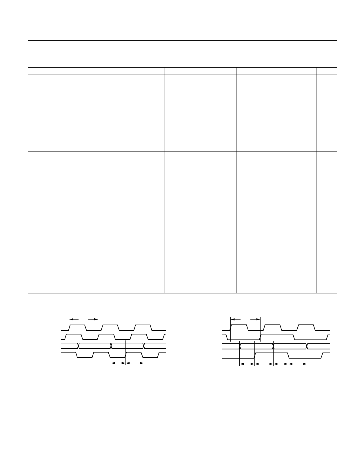
DIGITAL TIMING INFORMATION
t
DCO
CLK
DATACLK_OU
DB[15:0]
DATACLK_IN
Figure 2. Single Datarate (SDR) Mode
t
DCO
CLK
DATACLK_OUT
DB[15:0]
DATACLK_IN
t
t
DH
DS
04540-0-002
Rev. PrA | Page 5 of 16
t
t
DS
Figure 3. Double Datarate (DDR) Mode
t
DH
DS
t
DH
04540-0-003
 Loading...