REFERENCE
IN
TRANSPARENT LATCHES
DECODERS
AND
DRIVERS
SWITCH
NETWORK
I
OUT
CONTROL
AMP OUT
REFERENCE
OUT
CONTROL
AMP IN
R
SET
LATCH
ENABLE
AD9712B/AD9713B
(MSB)
(LSB)
DIGITAL
INPUTS
D1
THRU
D
12
I
OUT
+
–
CONTROL
AMP
16
14
19
26
17
18
28
24
1
11
20
INTERNAL
VOLTAGE
REFERENCE
12-Bit, 100 MSPS
a
FEATURES
100 MSPS Update Rate
ECL/TTL Compatibility
SFDR @ 1 MHz: 70 dBc
Low Glitch Impulse: 28 pV-s
Fast Settling: 27 ns
Low Power: 725 mW
1/2 LSB DNL (B Grade)
40 MHz Multiplying Bandwidth
APPLICATIONS
ATE
Signal Reconstruction
Arbitrary Waveform Generators
Digital Synthesizers
Signal Generators
GENERAL DESCRIPTION
The AD9712B and AD9713B D/A converters are replacements
for the AD9712 and AD9713 units which offer improved ac and
dc performance. Like their predecessors, they are 12-bit, high
speed digital-to-analog converters fabricated in an advanced
oxide isolated bipolar process. The AD9712B is an ECLcompatible device featuring update rates of 100 MSPS minimum; the TTL-compatible AD9713B will update at 80 MSPS
minimum.
D/A Converters
AD9712B/AD9713B
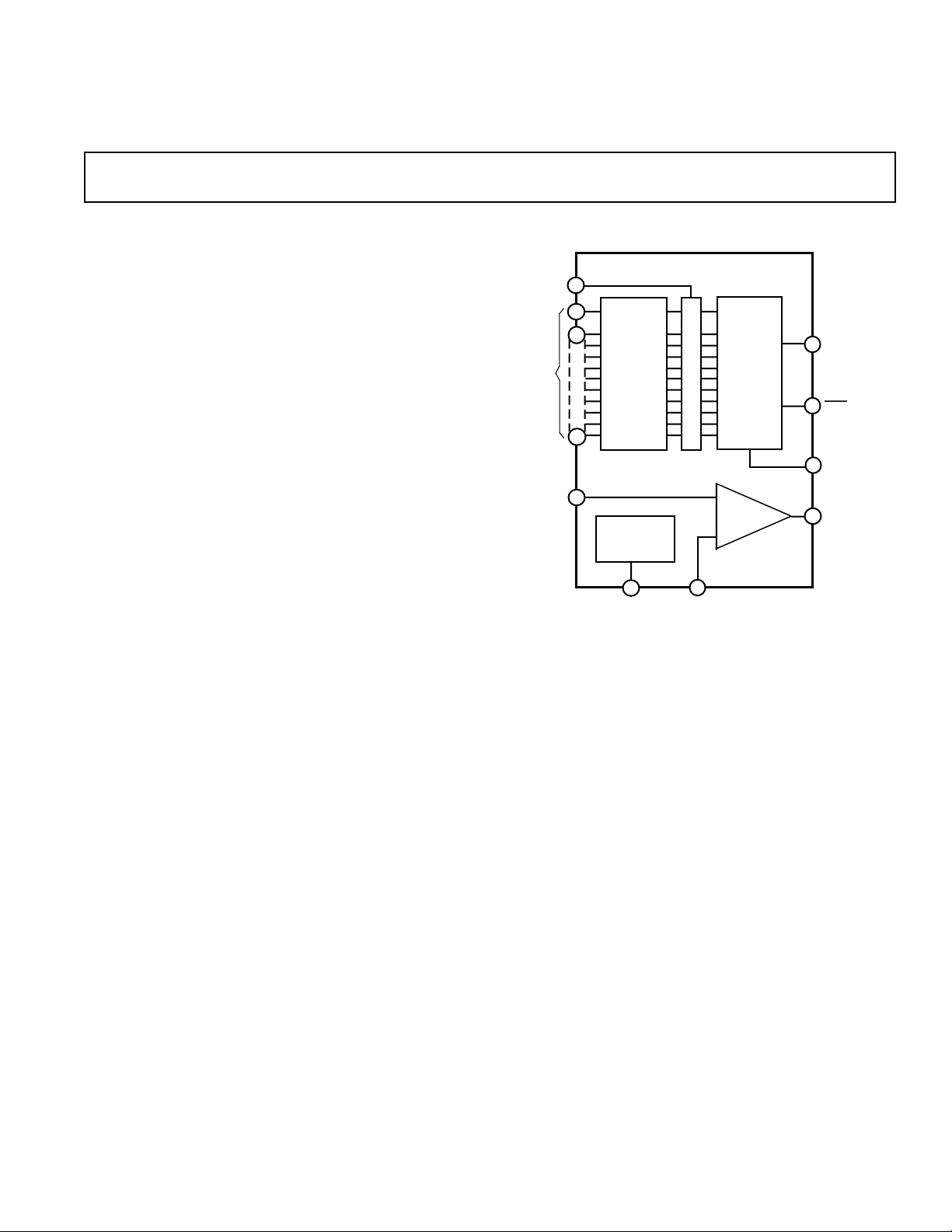
FUNCTIONAL BLOCK DIAGRAM
REV. B
Information furnished by Analog Devices is believed to be accurate and
reliable. However, no responsibility is assumed by Analog Devices for its
use, nor for any infringements of patents or other rights of third parties
which may result from its use. No license is granted by implication or
otherwise under any patent or patent rights of Analog Devices.
Designed for direct digital synthesis, waveform reconstruction,
and high resolution imaging applications, both devices feature
low glitch impulse of 28 pV-s and fast settling times of 27 ns.
Both units are characterized for dynamic performance and have
excellent harmonic suppression.
The AD9712B and AD9713B are available in 28-pin plastic
DIPs and PLCCs, with an operating temperature range of
–25°C to +85°C. Both are also available for extended temperature ranges of –55°C to +125°C in cerdips and 28-pin LCC
packages.
One Technology Way, P.O. Box 9106, Norwood, MA 02062-9106, U.S.A.
Tel: 617/329-4700 Fax: 617/326-8703

AD9712B/AD9713B–SPECIFICA TIONS
[–VS = –5.2 V; +VS = +5 V (AD9713B only); Reference Voltage = –1.2 V;
R
ELECTRICAL CHARACTERISTICS
= 7.5 kV; V
SET
AD9712B/AD9713B AD9712B/AD9713B AD9712B/AD9713B AD9712B/AD9713B
Test AN/AP BN/BP SE/SQ TE/TQ
Parameter (Conditions) Temp Level Min Typ Max Min Typ Max Min Typ Max Min Typ Max Units
RESOLUTION 12 12 12 12 Bits
DC ACCURACY
Differential Nonlinearity +25°C I –1.25 1.0 +1.25 –0.75 0.5 +0.75 –1.5 1.0 +1.5 –1.0 0.5 +1.0 LSB
Full VI –2.0 2.0 –1.5 1.5 –2.0 2.0 –1.5 1.5 LSB
Integral Nonlinearity +25°C I –1.5 1.0 1.5 –1.0 0.75 1.0 –1.75 1.5 1.75 –1.25 1.0 1.25 LSB
(“Best Fit” Straight Line) Full VI –2.0 2.0 –1.75 1.75 –2.0 2.0 –1.75 1.75 LSB
Test All Grades All Grades
Parameter (Conditions) Temp Level Min Typ Max Min Typ Max Units
INITIAL OFFSET ERROR
Zero-Scale Offset Error +25°C I 0.5 2.5 0.5 2.5 µA
Full VI 5.0 5.0 µA
+25°C I 1.0 5 1.0 5 %
Full-Scale Gain Error
1
Full VI 8 8 %
Offset Drift Coefficient +25°C V 0.01 0.01 µA/°C
REFERENCE/CONTROL AMP
Internal Reference Voltage +25°C I –1.14 –1.18 –1.22 –1.14 –1.18 –1.22 V
Full VI –1.12 –1.24 –1.12 –1.24 V
Internal Reference Voltage Drift Full V 50 50 ppm/°C
Internal Reference Output Current Full IV –50 +500 –50 +500 µA
Amplifier Input Impedance +25°C V 50 50 kΩ
Amplifier Bandwidth +25°C V 300 300 kHz
REFERENCE INPUT
Reference Input Impedance +25°CV 3 3 kΩ
Reference Multiplying Bandwidth
DYNAMIC PERFORMANCE
Full-Scale Output Current
2
3
4
+25°C V 40 40 MHz
+25°C V 20.48 20.48 mA
Output Compliance Range +25°C IV –1.2 +2 –1.2 +2 V
Output Resistance +25°C IV 2.0 2.5 3.0 2.0 2.5 3.0 kΩ
Output Capacitance +25°C V 15 15 pF
Output Update Rate
Output Settling Time (tST)
Output Propagation Delay (tPD)
Glitch Impulse
Output Rise Time
Output Fall Time
5
6
7
8
9
9
+25°C IV 100 110 80 100 MSPS
+25°C V 27 27 ns
+25°CV 6 7 ns
+25°C V 28 28 pV-s
+25°CV 2 2 ns
+25°CV 2 2 ns
DIGITAL INPUTS
Logic “1” Voltage Full VI –1.0 –0.8 2.0 V
Logic “0” Voltage Full VI –1.7 –1.5 0.8 V
Logic “1” Current Full VI 20 20 µA
Logic “0” Current Full VI 10 600 µA
Input Capacitance +25°CV 3 3 pF
Input Setup Time (tS)
Input Hold Time (tH)
10
11
+25°C IV 0.5 –0.3 0.5 –0.3 ns
Full IV 0.8 0.8 ns
+25°C IV 1.8 1.2 1.8 1.2 ns
Full IV 2.0 2.0 ns
Latch Pulse Width (t
) (LOW) +25°C IV 2.5 1.7 2.5 1.7 ns
LPW
(Transparent) Full 2.8 2.8 ns
AC LINEARITY
12
Spurious-Free Dynamic Range (SFDR)
1.23 MHz; 10 MSPS; 2 MHz Span +25 °C V 70 70 dB
5.055 MHz; 20 MSPS; 2 MHz Span +25°C V 72 72 dB
10.1 MHz; 50 MSPS; 2 MHz Span +25 °C V 68 68 dB
16 MHz; 40 MSPS; 10 MHz Span +25° C V 68 68 dB
= 0 V (virtual ground); unless otherwise noted]
OUT
AD9712B AD9713B
–2–
REV. B

AD9712B/AD9713B
Test All Grades All Grades
AD9712B AD9713B
Parameter (Conditions) Temp Level Min Typ Max Min Typ Max Units
POWER SUPPLY
13
Positive Supply Current (+5.0 V) +25°CI 6 12 mA
Negative Supply Current (–5.2 V)
14
Full VI 14 mA
+25°C I 140 178 145 184 mA
Full VI 183 188 mA
Nominal Power Dissipation +25°C V 728 784 mW
Power Supply Rejection Radio (PSRR)15+25°C I 30 100 30 100 µA/V
NOTES
1
Measured as error in ratio of full-scale current to current through R
2
Full-scale variations among devices are higher when driving REFERENCE INPUT directly.
3
Frequency at which the gain is flat ±0.5 dB; RL = 50 Ω; 50% modulation at midscale.
4
Based on IFS = 128 (V
5
Data registered into DAC accurately at this rate; does not imply settling to 12-bit accuracy.
6
Measured as voltage settling at midscale transition to ±0.024%, RL = 50 Ω.
7
Measured as the time between the 50% point of the falling edge of LATCH ENABLE and the point where the output signal has left a 1 LSB error band
around its previous value.
8
Peak glitch impulse is measured as the largest area under a single positive or negative transient.
9
Measured with RL = 50 Ω and DAC operating in latched mode.
10
Data must remain stable for specified time prior to falling edge of LATCH ENABLE signal.
11
Data must remain stable for specified time after rising edge of LATCH ENABLE signal.
12
SFDR is defined as the difference in signal energy between the fundamental and worst case spurious frequencies in the output spectrum window, which is
centered at the fundamental frequency and covers the indicated span.
13
Supply voltages should remain stable within ±5% for normal operation.
14
108 mA typ on Digital –VS, 37 mA typ on Analog –VS.
15
Measured at ±5% of +VS (AD9713B only) and –VS (AD9712B or AD9713B) using external reference.
Specifications subject to change without notice.
ABSOLUTE MAXIMUM RATINGS
) when using internal amplifier.
REF/RSET
1
Positive Supply Voltage (+VS) (AD9713B Only) . . . . . . . +6 V
Negative Supply Voltage (–V
) . . . . . . . . . . . . . . . . . . . . . –7 V
S
Analog-to-Digital Ground Voltage Differential . . . . . . . . 0.5 V
Digital Input Voltages (D
, LATCH ENABLE)
1–D12
AD9712B . . . . . . . . . . . . . . . . . . . . . . . . . . . . . . . 0 V to –V
AD9713B . . . . . . . . . . . . . . . . . . . . . . . . . . . . .–0.5 V to +V
Internal Reference Output Current . . . . . . . . . . . . . . . .500 µA
Control Amplifier Input Voltage Range . . . . . . . . . 0 V to –4 V
Control Amplifier Output Current . . . . . . . . . . . . . . . ±2.5 mA
Reference Input Voltage Range (V
) . . . . . . . . . . . 0 V to –V
REF
Analog Output Current . . . . . . . . . . . . . . . . . . . . . . . . . 30 mA
Operating Temperature Range
AD9712B/AD9713BAN/AP/BN/BP . . . . . . .–25°C to +85°C
AD9712B/AD9713BSE/SQ/TE/TQ . . . . . .–55°C to +125°C
Maximum Junction Temperature
2
AD9712B/AD9713BAN/AP/BN/BP . . . . . . . . . . . . . +150°C
AD9712B/AD9713BSE/SQ/TE/TQ . . . . . . . . . . . . . +175°C
Lead Temperature (Soldering, 10 sec) . . . . . . . . . . . . . +300°C
(160 µA nominal); ratio is nominally 128.
SET
Model Range Description Option
AD9712BAN –25°C to +85°C 28-Pin PDIP N-28
AD9712BBN –25°C to +85°C 28-Pin PDIP N-28
S
AD9712BAP –25°C to +85°C 28-Pin PLCC P-28A
S
AD9712BBP –25°C to +85°C 28-Pin PLCC P-28A
AD9712BSQ/883B –55°C to +125°C 28-Pin Cerdip Q-28
AD9712BSE/883B –55°C to +125°C 28-Pin LCC E-28A
AD9712BTQ/883B –55°C to +125°C 28-Pin Cerdip Q-28
S
AD9712BTE/883B –55°C to +125°C 28-Pin LCC E-28A
AD9713BAN –25°C to +85°C 28-Pin PDIP N-28
AD9713BBN –25°C to +85°C 28-Pin PDIP N-28
AD9713BAP –25°C to +85°C 28-Pin PLCC P-28A
AD9713BBP –25°C to +85°C 28-Pin PLCC P-28A
AD9713BSQ/883B –55°C to +125°C 28-Pin Cerdip Q-28
AD9713BSE/883B –55°C to +125°C 28-Pin LCC E-28A
AD9713BTQ/883B –55°C to +125°C 28-Pin Cerdip Q-28
AD9713BTE/883B –55°C to +125°C 28-Pin LCC E-28A
ORDERING GUIDE
Temperature Package Package
Storage Temperature Range . . . . . . . . . . . . .–65°C to +150°C
NOTES
1
Absolute maximum ratings are limiting values to be applied individually, and
beyond which the serviceability of the circuit may be impaired. Functional
operability is not necessarily implied. Exposure to absolute maximum rating
conditions for an extended period of time may affect device reliability.
2
Typical thermal impedances with parts soldered in place: 28-pin plastic DIP:
θJA = 37°C/W, θJC = 10°C/W; 28-pin PLCC: θJA = 44°C/W, θJC = 14°C/W;
Cerdip: θJA = 32°C/W, θJC = 10°C/W; LCC: θJA = 41°C/W, θJC = 13°C/W. No air
flow.
EXPLANATION OF TEST LEVELS
Test Level
I – 100% production tested.
II – 100% production tested at +25°C, and sample tested at
specified temperatures.
III – Sample tested only.
IV – Parameter is guaranteed by design and characterization
testing.
V – Parameter is a typical value only.
VI – All devices are 100% tested at +25°C. 100% production
tested at temperature extremes for extended tempera-
ture devices; sample tested at temperature extremes for
commercial/industrial devices.
REV. B
–3–

AD9712B/AD9713B
Pin # Name Function
PIN DESCRIPTIONS
1–10 D2–D
11 D
(LSB) Least Significant Bit (LSB) of digital input word.
12
11
Ten bits of twelve-bit digital input word.
Input Coding vs. Current Output
Input Code D
1–D12
I
(mA) I
OUT
OUT
(mA)
1111111111 –20.475 0
0000000000 0 –20.475
12 DIGITAL –V
S
One of two negative digital supply pins; nominally –5.2 V.
13 ANALOG RETURN Analog ground return. This point and the reference side of the DAC load resistors should be
connected to the same potential (nominally ground).
14 I
OUT
15 ANALOG –V
16 I
OUT
S
Analog current output; full-scale output occurs with digital inputs at all “1.”
One of two negative analog supply pins; nominally –5.2 V.
Complementary analog current output; zero scale output occurs with digital inputs at all “1.”
17 REFERENCE IN Normally connected to CONTROL AMP OUT (Pin 18). Direct line to DAC current source
network. Voltage changes at this point have a direct effect on the full-scale output value of
unit. Full-scale current output = 128 (Reference voltage/R
) when using internal amplifier.
SET
18 CONTROL AMP OUT Normally connected to REFERENCE INPUT (Pin 17). Output of internal control amplifier,
which provides a temperature-compensated drive level to the current switch network.
19 CONTROL AMP IN Normally connected to REFERENCE OUT (Pin 20) if not connected to external reference.
20 REFERENCE OUT Normally connected to CONTROL AMP IN (Pin 19). Internal voltage reference, nominally
–1.18 V.
21 DIGITAL –V
S
One of two negative digital supply pins; nominally –5.2 V.
22 REFERENCE GROUND Ground return for the internal voltage reference and amplifier.
23 DIGITAL +V
S
Positive digital supply pin, used only on the AD9713B; nominally +5 V. No connection to this
pin on AD9712B.
24 R
SET
25 ANALOG –V
S
Connection for external resistance reference. Full-scale current out = 128 (Reference voltage/
R
) when using internal amplifier. Nominally 7.5 kΩ.
SET
One of two negative analog supply pins; nominally –5.2 V.
26 LATCH ENABLE Transparent latch control line. Register is transparent when LATCH ENABLE is LOW.
27 DIGITAL GROUND Digital ground return.
28 D1 (MSB) Most Significant Bit (MSB) of digital input word.
D
D
D12 (LSB)
DIGITAL –V
ANALOG RETURN
I
OUT
D
D
D
D
D
D
D
D
10
11
2
3
4
5
6
7
8
9
S
1
2
3
4
5
AD9712B
6
AD9713B
7
8
(Not to Scale)
9
10
11
12
13
14
DIP
TOP VIEW
D1 (MSB0)
28
27
DIGITAL GROUND
26
LATCH ENABLE
25
ANALOG –V
R
24
SET
23
DIGITAL +V
REFERENCE GROUND
22
21
DIGITAL –V
20
REFERENCE OUT
CONTROL AMP IN
19
18
CONTROL AMP OUT
17
REFERENCE IN
I
16
OUT
15
ANALOG –V
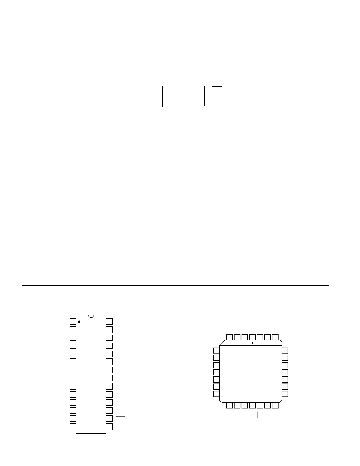
PIN CONFIGURATIONS
S
S
S
S
–4–
D
D
D (LSB)
12
PLCC/LCC
4
5
D
4
5
D
6
6
D
7
7
D
8
8
D
9
9
10
10
11
11
12
13 141516 17 18
S
DIGITAL –V
3
D
D
D
1
23
AD9712B
AD9713B
TOP VIEW
(Not to Scale)
S
OUT
I
RETURN
ANALOG
ANALOG –V
2
1
D (MSB)
28 27
OUT
I
ENABLE
LATCH
GROUND
DIGITAL
26
25
24
23
22
21
20
19
AMP OUT
CONTROL
REFERENCE IN
ANALOG –V
R
SET
DIGITAL +V
REFERENCE
GROUND
DIGITAL –V
REFERENCE
OUT
CONTROL
AMP IN
S
S
S
REV. B
 Loading...