ANALOG DEVICES AD9709 Service Manual
8-Bit, 125 MSPS, Dual TxDAC+
W
FEATURES
8-bit dual transmit digital-to-analog converter (DAC)
125 MSPS update rate
Excellent SFDR to Nyquist @ 5 MHz output: 66 dBc
Excellent gain and offset matching: 0.1%
Fully independent or single-resistor gain control
Dual port or interleaved data
On-chip 1.2 V reference
Single 5 V or 3.3 V supply operation
Power dissipation: 380 mW @ 5 V
Power-down mode: 50 mW @ 5 V
48-lead LQFP
APPLICATIONS
Communications
Base stations
Digital synthesis
Quadrature modulation
3D ultrasound
Digital-to-Analog Converter
AD9709
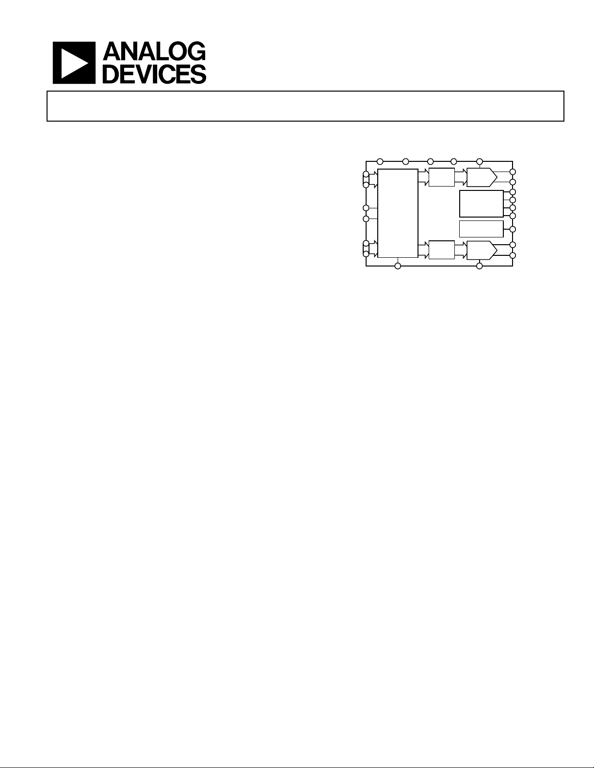
FUNCTIONAL BLOCK DIAGRAM
DCOM1/
PORT1
RT1/IQWRT
WRT2/IQSEL
PORT2
DVDD1/
DCOM2
DVDD2 AVDD ACOM
1
LATCH
DIGITAL
INTERFACE
AD9709
2
LATCH
Figure 1.
CLK1
1
DAC
REFERENCE
BIAS
GENERATOR
2
DAC
CLK2/IQ RESETMODE
I
OUTA1
I
OUTB1
REFIO
FSADJ1
FSADJ2
GAINCTRL
SLEEP
I
OUTA2
I
OUTB2
0606-001
GENERAL DESCRIPTION
The AD97091 is a dual-port, high speed, 2-channel, 8-bit CMOS
DAC. It integrates two high quality 8-bit TxDAC+® cores, a voltage
reference, and digital interface circuitry into a small 48-lead LQFP
package. The AD9709 offers exceptional ac and dc performance
while supporting update rates of up to 125 MSPS.
The AD9709 has been optimized for processing I and Q data in
communications applications. The digital interface consists of two
double-buffered latches as well as control logic. Separate write
inputs allow data to be written to the two DAC ports independent
of one another. Separate clocks control the update rate of the DACs.
A mode control pin allows the AD9709 to interface to two separate
data ports, or to a single interleaved high speed data port. In interleaving mode, the input data stream is demuxed into its original
I and Q data and then latched. The I and Q data is then converted
by the two DACs and updated at half the input data rate.
The GAINCTRL pin allows two modes for setting the full-scale
current (I
independently using two external resistors, or I
DACs can be set by using a single external resistor. See the Gain
Control Mode section for important date code information on
this feature.
The DACs utilize a segmented current source architecture
combined with a proprietary switching technique to reduce
1
Patent pending.
) of the two DACs. I
OUTFS
for each DAC can be set
OUTFS
for both
OUTFS
glitch energy and to maximize dynamic accuracy. Each DAC
provides differential current output, thus supporting singleended or differential applications. Both DACs can be
simultaneously updated and provide a nominal full-scale
current of 20 mA. The full-scale currents between each DAC
are matched to within 0.1%.
The AD9709 is manufactured on an advanced low-cost CMOS
process. It operates from a single supply of 3.3 V or 5 V and
consumes 380 mW of power.
PRODUCT HIGHLIGHTS
1. The AD9709 is a member of a pin-compatible family of
dual TxDACs providing 8-, 10-, 12-, and 14-bit resolution.
2. Dual 8-Bit, 125 MSPS DACs. A pair of high performance
DACs optimized for low distortion performance provide
for flexible transmission of I and Q information.
3. Matching. Gain matching is typically 0.1% of full scale, and
offset error is better than 0.02%.
4. Low Power. Complete CMOS dual DAC function operates
at 380 mW from a 3.3 V or 5 V single supply. The DAC
full-scale current can be reduced for lower power operation,
and a sleep mode is provided for low power idle periods.
5. On-Chip Voltage Reference. The AD9709 includes a 1.20 V
temperature-compensated band gap voltage reference.
6. Dual 8-Bit Inputs. The AD9709 features a flexible dual-
port interface, allowing dual or interleaved input data.
Rev. B
Information furnished by Analog Devices is believed to be accurate and reliable. However, no
responsibility is assumed by Analog Devices for its use, nor for any infringements of patents or other
rights of third parties that may result from its use. Specifications subject to change without notice. No
license is granted by implication or otherwise under any patent or patent rights of Analog Devices.
Trademarks and registered trademarks are the property of their respective owners.
One Technology Way, P.O. Box 9106, Norwood, MA 02062-9106, U.S.A.
Tel: 781.329.4700 www.analog.com
Fax: 781.461.3113 ©2000–2009 Analog Devices, Inc. All rights reserved.

AD9709
TABLE OF CONTENTS
Features .............................................................................................. 1
Applicat ions ....................................................................................... 1
Functional Block Diagram .............................................................. 1
General Description ......................................................................... 1
Product Highlights ........................................................................... 1
Revision History ............................................................................... 2
Specifications ..................................................................................... 3
DC Specifications ......................................................................... 3
Dynamic Specifications ............................................................... 4
Digital Specifications ................................................................... 5
Absolute Maximum Ratings ............................................................ 6
Thermal Resistance ...................................................................... 6
ESD Caution .................................................................................. 6
Pin Configuration and Function Descriptions ............................. 7
Typical Performance Characteristics ............................................. 8
Terminology .................................................................................... 11
Theory of Operation ...................................................................... 12
Functional Description .............................................................. 12
Reference Operation .................................................................. 13
Gain Control Mode .................................................................... 13
Setting the Full-Scale Current ................................................... 13
DAC Transfer Function ............................................................. 14
Analog Outputs .......................................................................... 14
Digital Inputs .............................................................................. 15
DAC Timing ................................................................................ 15
Sleep Mode Operation ............................................................... 18
Power Dissipation....................................................................... 18
Applying the AD9709 .................................................................... 19
Output Configurations .............................................................. 19
Differential Coupling Using a Transformer ............................ 19
Differential Coupling Using an Op Amp ................................ 19
Single-Ended, Unbuffered Voltage Output ............................. 20
Single-Ended, Buffered Voltage Output Configuration ........ 20
Power and Grounding Considerations .................................... 20
Applications Information .............................................................. 22
Quadrature Amplitude Modulation (QAM) Using the
AD9709 ........................................................................................ 22
CDMA ......................................................................................... 23
Evaluation Board ............................................................................ 24
General Description ................................................................... 24
Schematics ................................................................................... 24
Evaluation Board Layout ........................................................... 30
Outline Dimensions ....................................................................... 32
Ordering Guide .......................................................................... 32
REVISION HISTORY
9/09—Rev. A to Rev. B
Changes to Power and Grounding Considerations Section ..... 20
Changes to Schematics Section ..................................................... 24
Changes to Evaluation Board Layout Section ............................. 30
1/08—Rev. 0 to Rev. A
Updated Format .................................................................. Universal
Changed Single Supply Operation to 5 V or 3.3 V ........ Universal
Changes to Figure 1 .......................................................................... 1
Added Timing Diagram Section .................................................... 5
Changes to Figure 3 and Table 6 ..................................................... 7
Change to Figure 12 ......................................................................... 9
Changes to Figure 18 to Figure 20 ................................................ 10
Changes to Functional Description Section ............................... 13
Changes to Reference Operation Section .................................... 13
Changes to Figure 23 and Figure 24 ............................................. 13
Changes to Gain Control Mode Section ...................................... 13
Rev. B | Page 2 of 32
Replaced Reference Control Amplifier Section with Setting
the Full-Scale Current Section ...................................................... 13
Changes to DAC Transfer Function Section............................... 14
Changes to Interleaved Mode Timing Section ........................... 16
Added Figure 28 ............................................................................. 16
Changes to Power and Grounding Considerations Section ..... 20
Changes to Figure 44 ...................................................................... 22
Deleted Figure 43 ............................................................................ 17
Changes to CDMA Section ........................................................... 23
Changes to Figure 45 Caption ...................................................... 23
Changes to Figure 46 ...................................................................... 24
Changes to Figure 48 ...................................................................... 26
Updated Outline Dimensions ....................................................... 30
Changes to Ordering Guide .......................................................... 30
5/00—Revision 0: Initial Version

AD9709
SPECIFICATIONS
DC SPECIFICATIONS
T
to T
MIN
Table 1.
Parameter Min Typ Max Unit
RESOLUTION 8 Bits
DC ACCURACY1
Integral Linearity Error (INL) −0.5 ±0.1 +0.5 LSB
Differential Nonlinearity (DNL) −0.5 ±0.1 +0.5 LSB
ANALOG OUTPUT
Offset Error −0.02 +0.02 % of FSR
Gain Error Without Internal Reference −2 ±0.25 +2 % of FSR
Gain Error with Internal Reference −5 +1 +5 % of FSR
Gain Match
Full-Scale Output Current2 2.0 20.0 mA
Output Compliance Range −1.0 +1.25 V
Output Resistance 100 kΩ
Output Capacitance 5 pF
REFERENCE OUTPUT
Reference Voltage 1.14 1.20 1.26 V
Reference Output Current3 100 nA
REFERENCE INPUT
Input Compliance Range 0.1 1.25 V
Reference Input Resistance 1 MΩ
Small-Signal Bandwidth 0.5 MHz
TEMPERATURE COEFFICIENTS
Offset Drift 0 ppm of FSR/°C
Gain Drift Without Internal Reference ±50 ppm of FSR/°C
Gain Drift with Internal Reference ±100 ppm of FSR/°C
Reference Voltage Drift ±50 ppm/°C
POWER SUPPLY
Supply Voltages
AVDD 3 5 5.5 V
DVDD1, DVDD2 2.7 5 5.5 V
Analog Supply Current (I
Digital Supply Current (I
Digital Supply Current (I
Supply Current Sleep Mode (I
Power Dissipation4 (5 V, I
Power Dissipation5 (5 V, I
Power Dissipation6 (5 V, I
Power Supply Rejection Ratio7—AVDD −0.4 +0.4 % of FSR/V
Power Supply Rejection Ratio7—DVDD1, DVDD2 −0.025 +0.025 % of FSR/V
OPERATING RANGE −40 +85 °C
1
Measured at I
2
Nominal full-scale current, I
3
An external buffer amplifier with input bias current <100 nA should be used to drive any external load.
4
Measured at f
5
Measured at f
6
Measured as unbuffered voltage output with I
7
±10% power supply variation.
, AVDD = 3.3 V or 5 V, DVDD1 = DVDD2 = 3.3 V or 5 V, I
MAX
= 20 mA, unless otherwise noted.
OUTFS
TA = 25°C −0.3 ±0.1 +0.3 % of FSR
T
to T
MIN
T
MIN
−1.6 +1.6 % of FSR
MAX
to T
−0.14 +0.14 dB
MAX
) 71 75 mA
AVDD
)4 5 7 mA
DVDD
)5 15 mA
DVDD
) 8 12 mA
AVDD
= 20 mA) 380 410 mW
OUTFS
= 20 mA) 420 450 mW
OUTFS
= 20 mA) 450 mW
OUTFS
, driving a virtual ground.
OUTA
= 25 MSPS and f
CLK
= 100 MSPS and f
CLK
, is 32 times the I
OUTFS
= 1.0 MHz.
OUT
= 1 MHz.
OUT
current.
REF
= 20 mA and R
OUTFS
= 50 Ω at I
LOAD
Rev. B | Page 3 of 32
OUTA
and I
, f
= 100 MSPS, and f
OUTB
CLK
= 40 MHz.
OUT

AD9709
DYNAMIC SPECIFICATIONS
T
to T
MIN
doubly terminated, unless otherwise noted.
Table 2.
Parameter Min Typ Max Unit
DYNAMIC PERFORMANCE
Maximum Output Update Rate (f
Output Settling Time (tST) to 0.1%1 35 ns
Output Propagation Delay (tPD) 1 ns
Glitch Impulse 5 pV-s
Output Rise Time (10% to 90%)1 2.5 ns
Output Fall Time (90% to 10%)1 2.5 ns
Output Noise (I
Output Noise (I
AC LINEARITY
Spurious-Free Dynamic Range to Nyquist
Signal to Noise and Distortion Ratio
Total Harmonic Distortion
Multitone Power Ratio (Eight Tones at 110 kHz Spacing)
Channel Isolation
1
Measured single-ended into 50 Ω load.
, AVDD = 3.3 V or 5 V, DVDD1 = DVDD2 = 3.3 V or 5 V, I
MAX
) 125 MSPS
CLK
= 20 mA) 50 pA/√Hz
OUTFS
= 2 mA) 30 pA/√Hz
OUTFS
f
= 100 MSPS, f
CLK
= 1.00 MHz
OUT
= 20 mA, differential transformer-coupled output, 50 Ω
OUTFS
0 dBFS Output 63 68 dBc
–6 dBFS Output 62 dBc
–12 dBFS Output 56 dBc
–18 dBFS Output 50 dBc
f
= 65 MSPS, f
CLK
f
= 65 MSPS, f
CLK
f
= 65 MSPS, f
CLK
f
= 65 MSPS, f
CLK
f
= 65 MSPS, f
CLK
f
= 125 MSPS, f
CLK
f
= 125 MSPS, f
CLK
f
= 50 MHz, f
CLK
f
= 100 MSPS, f
CLK
f
= 50 MSPS, f
CLK
f
= 125 MSPS, f
CLK
f
= 125 MSPS, f
CLK
f
= 65 MSPS, f
CLK
= 1.00 MHz 68 dBc
OUT
= 2.51 MHz 68 dBc
OUT
= 5.02 MHz 66 dBc
OUT
= 14.02 MHz 60 dBc
OUT
= 25 MHz 50 dBc
OUT
= 25 MHz 63 dBc
OUT
= 40 MHz 55 dBc
OUT
= 1 MHz 50 dB
OUT
= 1.00 MHz −67 −63 dBc
OUT
= 2.00 MHz −63 dBc
OUT
= 4.00 MHz −63 dBc
OUT
= 10.00 MHz −63 dBc
OUT
= 2.00 MHz to 2.99 MHz
OUT
0 dBFS Output 58 dBc
–6 dBFS Output 51 dBc
–12 dBFS Output 46 dBc
–18 dBFS Output 41 dBc
f
= 125 MSPS, f
CLK
f
= 125 MSPS, f
CLK
= 10 MHz 85 dBc
OUT
= 40 MHz 77 dBc
OUT
Rev. B | Page 4 of 32
AD9709
DIGITAL SPECIFICATIONS
T
to T
MIN
Table 3.
Parameter Min Typ Max Unit
DIGITAL INPUTS
Logic 1 Voltage @ DVDD1 = DVDD2 = 5 V 3.5 5 V
Logic 1 Voltage @ DVDD1 = DVDD2 = 3.3 V 2.1 3 V
Logic 0 Voltage @ DVDD1 = DVDD2 = 5 V 0 1.3 V
Logic 0 Voltage @ DVDD1 = DVDD2 = 3.3 V 0 0.9 V
Logic 1 Current −10 +10 μA
Logic 0 Current −10 +10 μA
Input Capacitance 5 pF
Input Setup Time (tS) 2.0 ns
Input Hold Time (tH) 1.5 ns
Latch Pulse Width (t
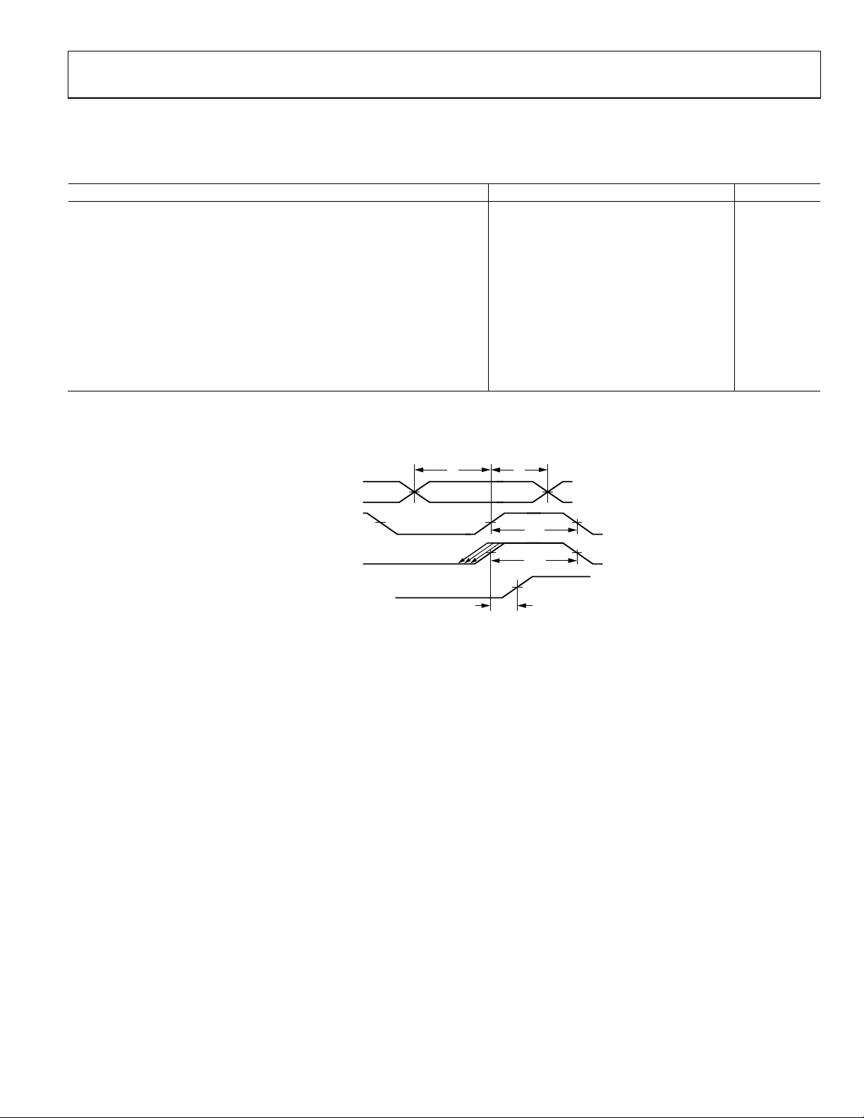
Timing Diagram
See Tab le 3 and the DAC Timing section for more information about the timing specifications.
, AVDD = 3.3 V or 5 V, DVDD1 = DVDD2 = 3.3 V or 5 V I
MAX
, t
) 3.5 ns
LPW
CPW
DATA IN
= 20 mA, unless otherwise noted.
OUTFS
t
S
t
H
(WRT2) (WRT1/IQWRT)
(CLK2) (CLK1/IQCLK)
I
OUTA
OR
I
OUTB
t
LPW
t
CPW
t
PD
00606-002
Figure 2. Timing for Dual and Interleaved Modes
Rev. B | Page 5 of 32
AD9709
ABSOLUTE MAXIMUM RATINGS
Table 4.
With
Parameter
AVDD ACOM −0.3 V to +6.5 V
DVDD1, DVDD2 DCOM1/DCOM2 −0.3 V to +6.5 V
ACOM DCOM1/DCOM2 −0.3 V to +0.3 V
AVDD DVDD1/DVDD2 −6.5 V to +6.5 V
MODE, CLK1/IQCLK,
CLK2/IQRESET,
WRT1/IQWRT,
WRT2/IQSEL
Digital Inputs DCOM1/DCOM2
I
OUTA1/IOUTA2
I
REFIO, FSADJ1,
FSADJ2
GAINCTRL, SLEEP ACOM −0.3 V to AVDD + 0.3 V
Junction Temperature 150°C
Storage Temperature
Range
Lead Temperature
(10 sec)
,
OUTB1/IOUTB2
Respect To
DCOM1/DCOM2
ACOM −1.0 V to AVDD + 0.3 V
ACOM −0.3 V to AVDD + 0.3 V
−65°C to +150°C
300°C
Rating
−0.3 V to DVDD1/
DVDD2 + 0.3 V
−0.3 V to DVDD1/
DVDD2 + 0.3 V
Stresses above those listed under Absolute Maximum Ratings
may cause permanent damage to the device. This is a stress
rating only; functional operation of the device at these or any
other conditions above those indicated in the operational
section of this specification is not implied. Exposure to absolute
maximum rating conditions for extended periods may affect
device reliability.
THERMAL RESISTANCE
θJA is specified for the worst-case conditions, that is, a device
soldered in a circuit board for surface-mount packages.
Table 5. Thermal Resistance
Package Type θJA Unit
48-Lead LQFP 91 °C/W
ESD CAUTION
Rev. B | Page 6 of 32

AD9709
PIN CONFIGURATION AND FUNCTION DESCRIPTIONS
OUTA1
MODE47AVDD46I
48
OUTB1
I
FSADJ143REFIO42GAINCTRL41FSADJ240I
45
44
OUTB2
OUTA2
I
ACOM37SLEEP
39
38
36
NC
35
NC
34
NC
33
NC
32
NC
31
NC
30
DB0P2 (LSB)
29
DB1P2
28
DB2P2
DB3P2
27
DB4P2
26
DB5P2
25
23
24
DB6P2
DVDD2
DB7P2 (MSB)
0606-003
DB6P1
DB5P1
DB4P1
DB3P1
DB2P1
DB1P1
DB0P1
NC
NC
NC
NC
1
2
3
4
5
6
7
8
9
10
11
12
DB7P1 (MSB)
NC = NO CONNECT
PIN 1
INDICATOR
13NC14NC15
AD9709
TOP VIEW
(Not to Scale)
16
17
DVDD1
DCOM1
18
19
20
21
22
DCOM2
CLK1/IQCLK
WRT2/IQSEL
WRT1/IQWRT
CLK2/IQRESET
Figure 3. Pin Configuration
Table 6. Pin Function Descriptions
Pin No. Mnemonic Description
1 to 8 DB7P1 to DB0P1 Data Bit Pins (Port 1)
9 to 14, 31 to 36 NC No Connection
15, 21 DCOM1, DCOM2 Digital Common
16, 22 DVDD1, DVDD2 Digital Supply Voltage
17 WRT1/IQWRT Input Write Signal for Port 1 (IQWRT in Interleaving Mode)
18 CLK1/IQCLK Clock Input for DAC1 (IQCLK in Interleaving Mode)
19 CLK2/IQRESET Clock Input for DAC2 (IQRESET in Interleaving Mode)
20 WRT2/IQSEL Input Write Signal for Port 2 (IQSEL in Interleaving Mode)
23 to 30 DB7P2 to DB0P2 Data Bit Pins (Port 2)
37 SLEEP Power-Down Control Input
38 ACOM Analog Common
39, 40 I
OUTA2
, I
Port 2 Differential DAC Current Outputs
OUTB2
41 FSADJ2 Full-Scale Current Output Adjust for DAC2
42 GAINCTRL Master/Slave Resistor Control Mode.
43 REFIO Reference Input/Output
44 FSADJ1 Full-Scale Current Output Adjust for DAC1
45, 46 I
OUTB1
, I
Port 1 Differential DAC Current Outputs
OUTA1
47 AVDD Analog Supply Voltage
48 MODE Mode Select (1 = dual port, 0 = interleaved)
Rev. B | Page 7 of 32
AD9709
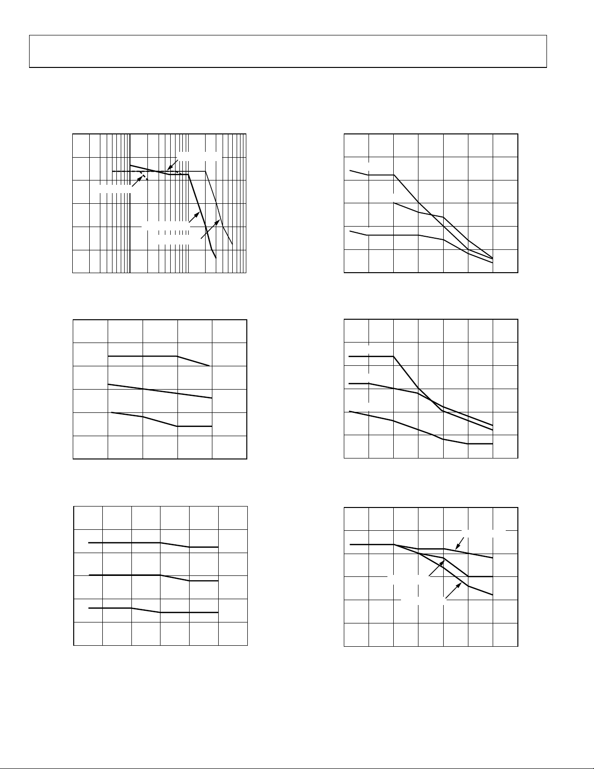
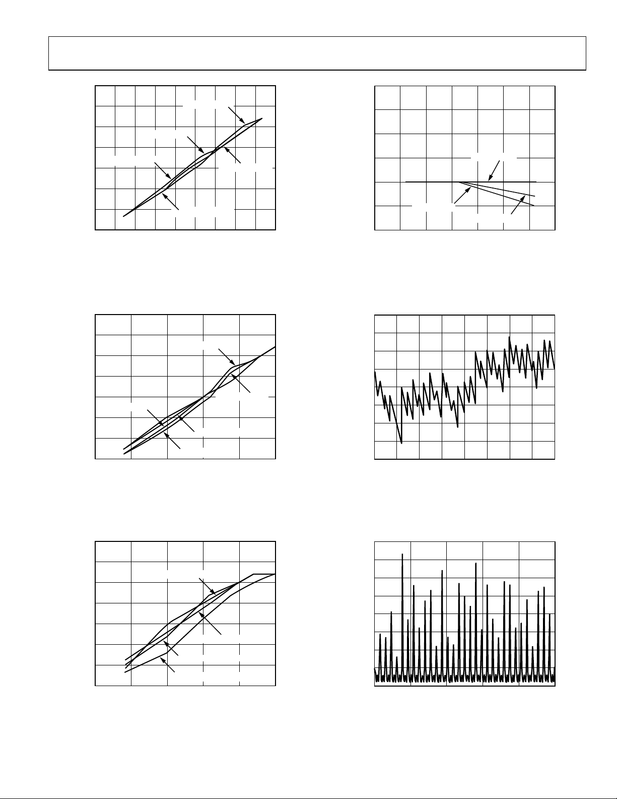
TYPICAL PERFORMANCE CHARACTERISTICS
AVDD = 3.3 V or 5 V, DVDD = 3.3 V, I
unless otherwise noted.
75
70
65
60
SFDR (dBc)
55
50
f
CLK
= 5MSPS
f
CLK
f
= 65MSPS
CLK
= 20 mA, 50 Ω doubly terminated load, differential output, TA = 25°C, SFDR up to Nyquist,
OUTFS
75
f
= 25MSPS
CLK
= 125MSPS
SFDR (dBc)
70
0dBFS
65
60
55
50
–6dBFS
–12dBFS
45
0.1 1 10 100
Figure 4. SFDR vs. f
75
70
65
60
SFDR (dBc)
55
50
45
0 0.5 1.0 1.5 2.0 2.5
0dBFS
–6dBFS
–12dBFS
Figure 5. SFDR vs. f
75
70
65
0dBFS
f
OUT
f
OUT
(MHz)
OUT
(MHz)
OUT
@ 0 dBFS
@ 5 MSPS
45
0 5 10 15 20 25 30 35
00606-005
Figure 7. SFDR vs. f
75
70
0dBFS
65
–6dBFS
60
SFDR (dBc)
00606-006
–12dBFS
55
50
45
0 10203040506070
Figure 8. SFDR vs. f
75
70
65
f
f
OUT
OUT
(MHz)
@ 65 MSPS
OUT
(MHz)
@ 125 MSPS
OUT
I
OUTFS
00606-008
00606-009
= 20mA
60
SFDR (dBc)
55
50
45
024681012
–6dBFS
–12dBFS
f
OUT
Figure 6. SFDR vs. f
(MHz)
@ 25 MSPS
OUT
00606-007
Rev. B | Page 8 of 32
60
SFDR (dBc)
55
50
45
0 5 10 15 20 25 30 35
Figure 9. SFDR vs. f
I
OUTFS
OUT
= 10mA
I
OUTFS
f
OUT
and I
= 5mA
(MHz)
@ 65 MSPS and 0 dBFS
OUTFS
00606-010
AD9709
75
70
70
65
60
25MSPS/2.27MHz
55
SFDR (dBc)
50
45
40
–25 –22 –19 –16 –13 –10 –7 –4 –1 2
10MSPS/0.91MHz
Figure 10. Single-Tone SFDR vs. A
75
70
65
60
55
SFDR (dBc)
10MSPS/2.0MHz
50
45
40
–25 –20 –15 –10 –5 0
Figure 11. Single-Tone SFDR vs. A
5MSPS/0.46MHz
125MSPS/11.37MHz
A
(dBFS)
OUT
OUT
5MSPS/1.0MHz
65MSPS/13.0MHz
25MSPS/5.0MHz
A
(dBFS)
OUT
OUT
65MSPS/5.91MHz
@ f
= f
OUT
125MSPS/5.0MHz
@ f
= f
OUT
65
60
I
55
SINAD (dBc)
50
45
40
0 20 40 60 80 100 120 140
00606-011
/11
CLK
/5
CLK
00606-012
Figure 13. SINAD vs. f
0.06
0.04
0.02
0
–0.02
INL (LSBs)
–0.04
–0.06
–0.08
–0.10
0 32 64 96 160 224128 192 256
I
= 5mA
OUTFS
f
(MSPS)
CLK
and I
CLK
OUTFS
CODE
Figure 14. Typical INL
= 20mA
OUTFS
I
= 10mA
OUTFS
@ f
= 5 MHz and 0 dBFS
OUT
00606-014
00606-015
75
70
65
60
55
SFDR (dBc)
50
45
40
–25 –20 –15 –10 –5 0
Figure 12. Dual-Tone SFDR vs. A
0.965MHz/1.035MHz @ 7MSPS
16.9MHz/19.1MHz @ 125MSPS
8.8MHz/9. 8M Hz @ 65MSPS
3.3MHz/3. 4M Hz @ 25MSPS
A
(dBFS)
OUT
@ f
OUT
OUT
= f
0.07
0.06
0.05
0.04
0.03
DNL (LSBs)
0.02
0.01
0
–0.01
0 50 100 150 200 250
/7
CLK
00606-013
Figure 15. Typical DNL
CODE
00606-016
Rev. B | Page 9 of 32
AD9709
75
70
65
60
SFDR (dBc)
55
50
45
–50 –30 –10 10 30 50 70 90
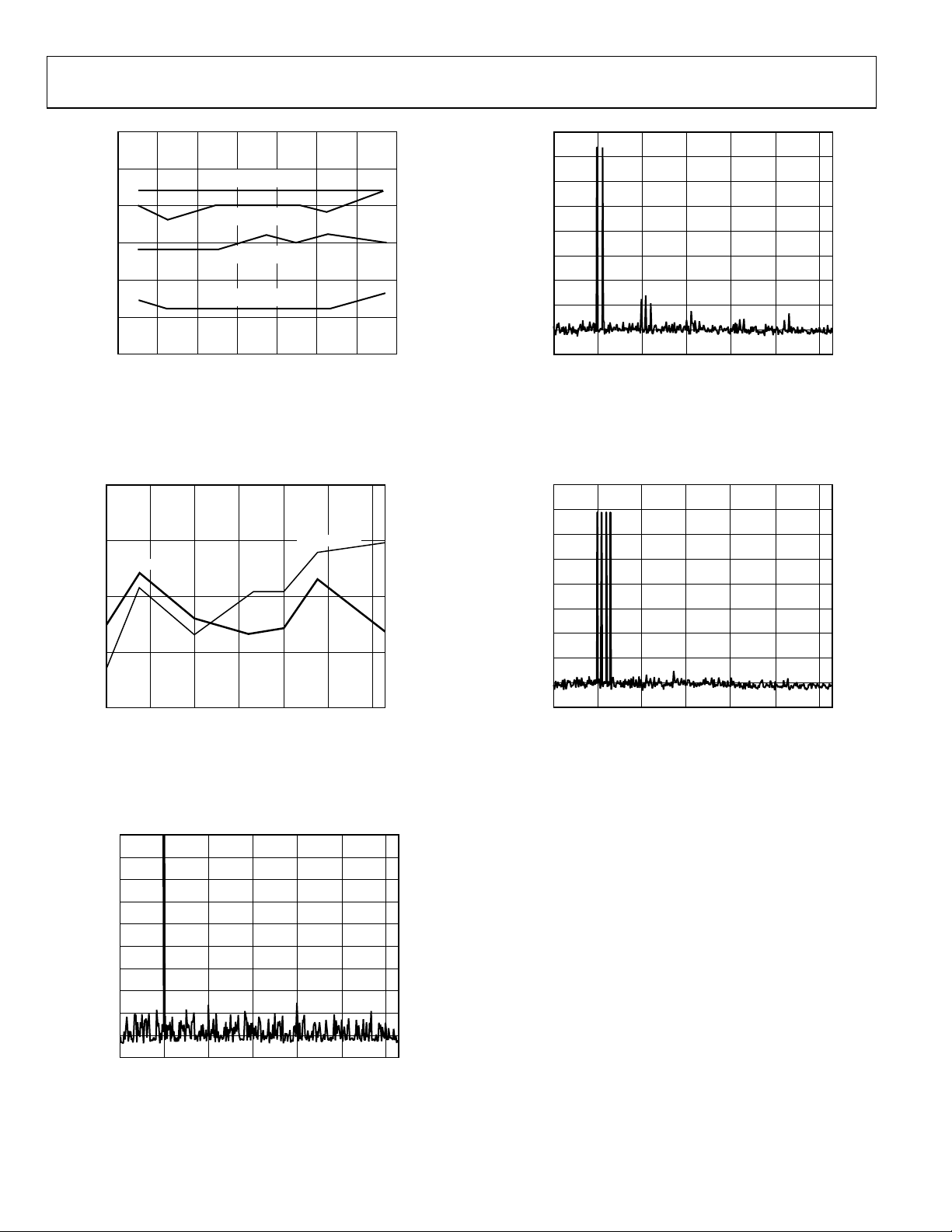
Figure 16. SFDR vs. Temperature @ f
0.05
0.03
OFFSET ERROR
0
OFFSET ERROR (%F S)
–0.03
–0.05
–40 –20 0 20 40 60 80
f
= 10MHz
OUT
f
= 25MHz
OUT
f
= 40MHz
OUT
f
= 60MHz
OUT
TEMPERATURE (°C)
TEMPERATURE (°C)
CLK
Figure 17. Gain and Offset Error vs. Temperature @ f
= 125 MSPS, 0 dBFS
GAIN ERROR
= 125 MSPS
CLK
1.0
0.5
0
–0.5
–1.0
0
–10
–20
–30
–40
–50
SFDR (dBm)
–60
–70
–80
–90
SFDR (dBm)
065040302010
Figure 19. Dual-Tone SFDR @ f
0
–10
–20
–30
–40
–50
–60
–70
–80
–90
065040302010
Figure 20. Four-Tone SFDR @ f
FREQUENCY (MHz)
CLK
FREQUENCY (MHz )
CLK
= 125 MSPS
= 125 MSPS
00606-017
GAIN ERROR (%F S )
0606-018
0
0606-020
0
00606-021
SFDR (dBm)
0
–10
–20
–30
–40
–50
–60
–70
–80
–90
–100
065040302010
Figure 18. Single-Tone SFDR @ f
FREQUENCY (MHz )
CLK
0
0606-019
= 125 MSPS
Rev. B | Page 10 of 32
 Loading...