Octal Ultrasound AFE
AD9670
Rev. PrB
Preliminary Technical Data
FEATURES
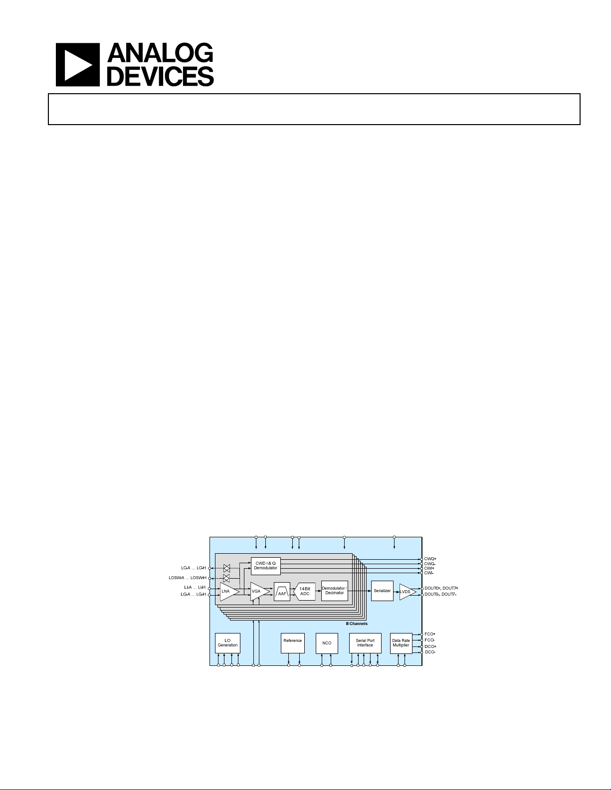
8 channels of LNA, VGA, AAF, ADC, and digital
demodulator/decimator
Low power: 130 mW per channel, TGC mode, 40 MSPS;
55mW per channel, CW mode; <5mW at power-up
10 mm × 10 mm, 144-ball CSP-BGA
TGC channel input-referred noise: 0.8 nV/√Hz, max gain
Flexible power-down modes
Fast recovery from low power standby mode: <2 μs
Low noise preamplifier (LNA)
Input-referred noise: 0.78 nV/√Hz, gain = 21.6 dB
Programmable gain: 15.6 dB/17.9 dB/21.6 dB
0.1 dB compression: 1000 mV p-p/750 mV p-p/450 mV p-p
Flexible active input impedance matching
Overload recovery: <10 ns
Variable gain amplifier (VGA)
Attenuator range: 45dB, Linear-in-dB gain control
Postamp gain (PGA): 21 dB/24 dB/27 dB/30 dB
Antialiasing filter (AAF)
Programmable second-order LPF from 8 MHz to 18 MHz or
13.5MHz to 30MHz and HPF
Analog-to-digital converter (ADC)
SNR: 75dB, 14 bits up to 125 MSPS
Configurable Serial LVDS
CW mode harmonic rejection I/Q demodulator
Individual programmable phase rotation
Output dynamic range per channel: >160 dBc/√Hz
Output-referred SNR: 156 dBc/√Hz, 1 kHz offset, −3dBFS
Digital demodulator/decimator
I/Q demodulator with programmable oscillator
FIR decimation filter: 16 taps per decimation factor
With Digital Demodulator
GENERAL DESCRIPTION
The AD9670 is designed for low cost, low power, small size,
and ease of use for medical ultrasound. It contains eight
channels of a variable gain amplifier (VGA) with a low noise
preamplifier (LNA), a CW harmonic rejection I/Q demodulator
with programmable phase rotation, an anti-aliasing filter
(AAF), an analog-to-digital converter (ADC), and a digital
demodulator and decimator for data processing and bandwidth
reduction.
Each channel features a maximum gain of up to 52 dB, a fully
differential signal path, and an active input preamplifier
termination. The channel is optimized for high dynamic
performance and low power in applications where a small
package size is critical.
The LNA has a single-ended-to-differential gain that is selectable
through the SPI. Assuming a 15 MHz noise bandwidth (NBW)
and a 21.6 dB LNA gain, the LNA input SNR is 94 dB. In CW
Doppler mode, each LNA output drives an I/Q demodulator
that has independently programmable phase rotation with 16
phase settings.
Power-down of individual channels is supported to increase
battery life for portable applications. Standby mode allows quick
power-up for power cycling. In CW Doppler operation, the
VGA, AAF, and ADC are powered down. The ADC contains
several features designed to maximize flexibility and minimize
system cost, such as a programmable clock, data alignment, and
programmable digital test pattern generation. The digital test
patterns include built-in fixed patterns, built-in pseudo random
patterns, and custom user-defined test patterns entered via the
serial port interface.
Information furnished by Analog Devices is believed to be accurate and reliable. However, no
responsibility is assumed by Analog Devices for its use, nor for any infringements of patents or other
rights of third parties that may result from its use. Specifications subject to change without notice. No
license is granted by implication or otherwise under any patent or patent rights of Analog Devices.
Trademarks and registered trademarks are the property of their respective owners.
AVDD2
AVDD1
R
R
E
E
S
S
E
E
T
T
-
+
GAIN-
GAIN+
M
M
L
L
O
O
-
+
PWDN
STDBY
V
R
R
B
E
I
A
F
S
DVDD
C
G
A
T
T
X
X
D
S
P
_
_
T
T
R
R
I
I
G
G
-
+
B
D
O
R
[
0
[
-
0
3
-
]
4
]
DRVDD
S
C
L
K
C
C
S
D
L
L
K
K
I
O
-
+
Figure 1.
One Technology Way, P.O. Box 9106, Norwood, MA 02062-9106, U.S.A.
Tel: 781.329.4700
Fax: 781.461.3113 ©2012 Analog Devices, Inc. All rights reserved.
www.analog.com

AD9670 Preliminary Technical Data
©2012 Analog Devices, Inc. All rights reserved. Trademarks and
registered trademarks are the property of their respective owners.
PR10946-0-7/12(PrB)
Rev. PrB | Page 2 of 2
 Loading...