

a
Ultrafast Comparators
AD96685/AD96687
FEATURES
Fast: 2.5 ns Propagation Delay
Low Power: 118 mW per Comparator
Packages: DIP, SOIC, PLCC
Power Supplies: +5 V, –5.2 V
Logic Compatibility: ECL
50 ps Delay Dispersion
APPLICATIONS
High Speed Triggers
High Speed Line Receivers
Threshold Detectors
Window Comparators
Peak Detectors
GENERAL DESCRIPTION
The AD96685 and AD96687 are ultrafast voltage comparators.
The AD96685 is a single comparator with 2.5 ns propagation
delay; the AD96687 is an equally fast dual comparator. Both
devices feature 50 ps propagation delay dispersion which is a
particularly important characteristic of high-speed comparators.
It is a measure of the difference in propagation delay under
differing overdrive conditions.
A fast, high precision differential input stage permits consistent
propagation delay with a wide variety of signals in the commonmode range from –2.5 V to +5 V. Outputs are complementary
digital signals fully compatible with ECL 10 K and 10 KH logic
families. The outputs provide sufficient drive current to directly
drive transmission lines terminated in 50 Ω to –2 V. A level
sensitive latch input which permits tracking, track-hold, or
sample-hold modes of operation is included.
The AD96685 is available in industrial –25°C to +85°C range
in 16-pin SOIC.
The AD96687 is available in industrial range –25°C to +85°C,
in 16-pin DIP, SOIC, and 20-lead PLCC.
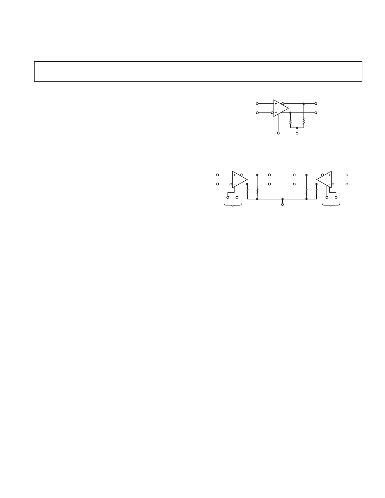
AD96685 FUNCTIONAL BLOCK DIAGRAM
NONINVERTING
AD96687 FUNCTIONAL BLOCK DIAGRAM
NONINVERTING
INPUT
INVERTING
INPUT
LE
LATCH
ENABLE
R
RLR
L
L
Q OUTPUT
Q OUTPUT
LE
LATCH
ENABLE
NONINVERTING
LE
INPUT
INVERTING
INPUT
R
L
Q OUTPUT
Q OUTPUT
V
T
V
T
LATCH
ENABLE
Q OUTPUT
Q OUTPUT
R
LRL
LE
THE OUTPUTS ARE OPEN EMITTERS, REQUIRING EXTERNAL
PULL-DOWN RESISTORS. THESE RESISTORS MAY BE IN THE
RANGE OF 50⍀-200⍀ CONNECTED TO –2.0V, OR 200⍀-2000⍀
INPUT
INVERTING
INPUT
REV. D
Information furnished by Analog Devices is believed to be accurate and
reliable. However, no responsibility is assumed by Analog Devices for its
use, nor for any infringements of patents or other rights of third parties that
may result from its use. No license is granted by implication or otherwise
under any patent or patent rights of Analog Devices.
One Technology Way, P.O. Box 9106, Norwood, MA 02062-9106, U.S.A.
Tel: 781/329-4700 www.analog.com
Fax: 781/326-8703 © Analog Devices, Inc., 2001
AD96685/AD96687–SPECIFICATIONS
ELECTRICAL CHARACTERISTICS
(Positive Supply Voltage = 5.0 V; Negative Supply Voltage = –5.2 V, unless otherwise noted.)
Industrial Temperature Range –25ⴗC to +85ⴗC
Test AD96685BR AD96687BQ/BP/BR
Parameter Temp Level Min Typ Max Min Typ Max Unit
INPUT CHARACTERISTICS
Input Offset Voltage 25°CI 12 12mV
Full VI 3 3 mV
Input Offset Drift Full V 20 20 µV/°C
Input Bias Current 25°CI 710 710µA
Full VI 13 13 µA
Input Offset Current 25°C I 0.1 1.0 0.1 1.0 µA
Full VI 1.2 1.2 µA
Input Resistance 25°C V 200 200 kΩ
Input Capacitance 25°CV 2 2 pF
Input Voltage Ranges
2
Full VI –2.5 +5.0 –2.5 +5.0 V
Common-Mode Rejection Ratio Full VI 80 90 80 90 dB
ENABLE INPUT
Logic “1” Voltage Full VI –1.1 –1.1 V
Logic “0” Voltage Full VI –1.5 –1.5 V
Logic “1” Current Full VI 40 40 µA
Logic “0” Current Full VI 5 5 µA
DIGITAL OUTPUTS
3
Logic “1” Voltage Full VI –1.1 –1.1 V
Logic “0” Voltage Full VI –1.5 –1.5 V
SWITCHING PERFORMANCES
Propagation Delays
4
Input to Output HIGH 25°C IV 2.5 3.5 2.5 3.5 ns
Input to Output LOW 25°C IV 2.5 3.5 2.5 3.5 ns
Latch Enable to Output HIGH 25°C IV 2.5 3.5 2.5 3.5 ns
Latch Enable to Output LOW 25°C IV 2.5 3.5 2.5 3.5 ns
Dispersions
5
25°C V 50 50 ps
Latch Enable
Minimum Pulsewidth 25°C IV 2.0 3.0 2.0 3.0 ns
Minimum Setup Time 25°C IV 0.5 1.0 0.5 1.0 ns
Minimum Hold Time 25°C IV 0.5 1.0 0.5 1.0 ns
POWER SUPPLY
6
Positive Supply Current (+5.0 V) Full VI 8 9 15 18 mA
Negative Supply Current (–5.2 V) Full VI 15 18 31 36 mA
Power Supply Rejection Ratio
NOTES
1
RS = 100 Ω.
2
Input Voltage Range can be extended to –3.3 V if –VS = –6.0 V.
3
Outputs terminated through 50 Ω to –2.0 V.
4
Propagation delays measured with 100 mV pulse (10 mV overdrive) to 50% transition point of the output.
5
Change in propagation delay from 100 mV to 1 V input overdrive.
6
Supply voltages should remain stable within ± 5% for normal operation.
7
Measured at ± 5% of +VS and –VS.
Specifications subject to change without notice.
7
Full VI 60 70 60 70 dB
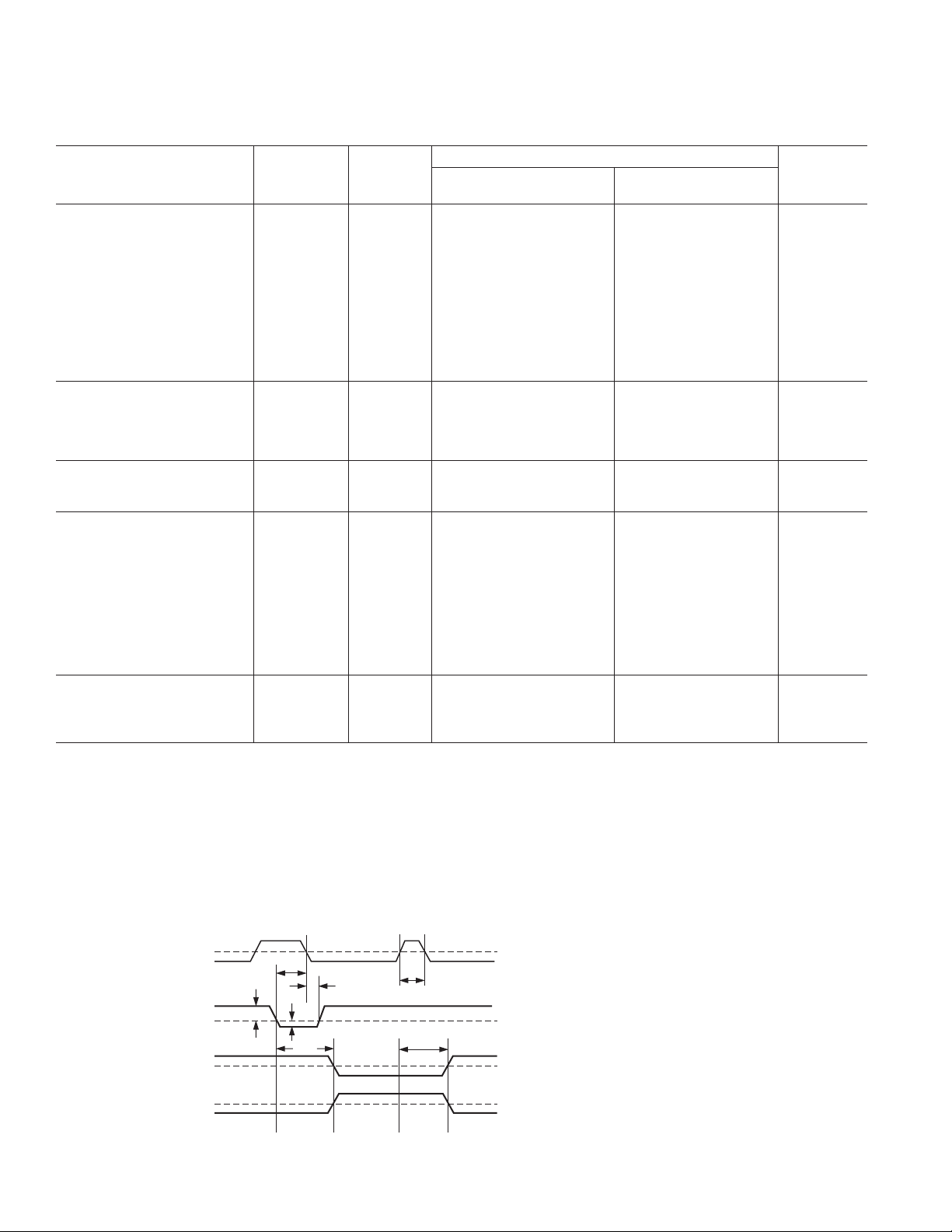
LATCH
ENABLE
DIFFERENTIAL
INPUT
VO LTAG E
COMPARE
LATCH
Q
Q
t
S
t
H
V
DD
V
IN
t
PD
t
(E)
PW
t
(E)
PD
50%
V
OS
50%
50%
t
– Minimum Setup Time
S
t
– Minimum Hold Time
H
t
– Input to Output Delay
PD
t
(E)
– LATCH ENABLE to Output Delay
PD
t
(E)
– Minimum LATCH ENABLE Pulsewidth
PW
V
– Input Offset Voltage
OS
V
– Overdrive Voltage
OD
Figure 1. System Timing Diagram
–2–
REV. D

AD96685/AD96687
ABSOLUTE MAXIMUM RATINGS
Positive Supply Voltage (+VS) . . . . . . . . . . . . . . . . . . . . . 6.5 V
Negative Supply Voltage (–V
Input Voltage Range
2
. . . . . . . . . . . . . . . . . . . . . . . . . . . . ±5 V
) . . . . . . . . . . . . . . . . . . . –6.5 V
S
Differential Input Voltage . . . . . . . . . . . . . . . . . . . . . . . . 5.5 V
Latch Enable Voltage . . . . . . . . . . . . . . . . . . . . . . . . –V
Output Current . . . . . . . . . . . . . . . . . . . . . . . . . . . . . . . 30 mA
Operating Temperature Range
AD96685BR/AD96687BQ/BR/BP . . . . . . . –25°C to +85°C
Storage Temperature Range . . . . . . . . . . . . –55°C to +150°C
Junction Temperature . . . . . . . . . . . . . . . . . . . . . . . . . . 175°C
Lead Soldering Temperature (10 sec) . . . . . . . . . . . . . . 300° C
NOTES
1
Absolute maximum ratings are limiting values, may be applied individually, and
beyond which serviceability of the circuit may be impaired. Functional operation
under any of these conditions is not necessarily implied. Exposure to absolute
maximum rating conditions for extended periods may affect device reliability.
2
Under no circumstances should the input voltages exceed the supply voltages.
3
Typical thermal impedances . . .
AD96685 SOIC qJA = 170°C/W; qJC = 60°C/W
AD96687 Ceramic qJA = 115°C/W; qJC = 57°C/W
AD96687 SOIC qJA = 92°C/W; qJC = 47°C/W
AD96687 PLCC qJA = 81°C/W; qJC = 45°C/W
1
EXPLANATION OF TEST LEVELS
Test Level
I – 100% production tested.
II – 100% production tested at 25°C, and sample tested at
specified temperatures.
to 0 V
S
3
III – Sample tested only.
IV – Parameter is guaranteed by design and characterization
testing.
V – Parameter is a typical value only.
VI – All devices are 100% production tested at 25°C; 100%
production tested at temperature extremes for extended
temperature devices; sample tested at temperature extremes for commercial/industrial devices.
FUNCTIONAL DESCRIPTION
Pin Name Description
+V
S
Positive supply terminal, nominally 5.0 V.
NONINVERTING INPUT Noninverting analog input of the differential input stage. The NONINVERTING INPUT must be
driven in conjunction with the INVERTING INPUT.
INVERTING INPUT Inverting analog input of the differential input stage. The INVERTING INPUT must be driven in
conjunction with the NONINVERTING INPUT.
LATCH ENABLE In the “compare” mode (logic HIGH), the output will track changes at the input of the compara-
tor. In the “latch” mode (logic LOW), the output will reflect the input state just prior to the
comparator being placed in the “latch” mode. LATCH ENABLE must be driven in conjunction
with LATCH ENABLE for the AD96687.
LATCH ENABLE In the “compare” mode (logic LOW), the output will track changes at the input of the comparator.
In the “latch” mode (logic HIGH), the output will reflect the input state just prior to the comparator
being placed in the “latch” mode. LATCH ENABLE must be driven in conjunction with
LATCH ENABLE for the AD96687.
–V
S
Negative supply terminal, nominally –5.2 V.
Q One of two complementary outputs. Q will be at logic HIGH if the analog voltage at the
NONINVERTING INPUT is greater than the analog voltage at the INVERTING INPUT (provided the comparator is in the “compare” mode). See LATCH ENABLE and LATCH ENABLE
(AD96687 only) for additional information.
Q One of two complementary outputs. Q will be at logic LOW if the analog voltage at the
NONINVERTING INPUT is greater than the analog voltage at the INVERTING INPUT
(provided the comparator is in the “compare” mode). See LATCH ENABLE and LATCH ENABLE
(AD96687 only) for additional information.
GROUND 1 One of two grounds, but primarily associated with the digital ground. Both grounds should be
connected together near the comparator.
GROUND 2 One of two grounds, but primarily associated with the analog ground. Both grounds should be
connected together near the comparator.
REV. D
–3–

AD96685/AD96687
PIN CONFIGURATIONS
GROUND 1
NONINVERTING
LATCH ENABLE
VS+
INPUT
INVERTING
INPUT
NC
NC
V
AD96685BR
1
2
3
AD96685
4
TOP VIEW
5
(Not to Scale)
6
7
–
8
S
NC = NO CONNECT
16
GROUND 2
15
NC
14
NC
13
NC
12
Q OUTPUT
Q OUTPUT
11
NC
10
NC
9
LATCH
ENABLE
NC
LATCH
ENABLE
V
4
5
6
7
8
–
S
GROUND
NC = NO CONNECT
AD96687BP
Q OUTPUT
Q OUTPUTNCQ OUTPUT
3 2 1 20 19
AD96687
TOP VIEW
(Not to Scale)
9 10 11 12 13
NC
INPUT
INPUT
INVERTING
NONINVERTING
NONINVERTING
Q OUTPUT
INPUT
INVERTING
18
17
16
15
14
INPUT
GROUND
LATCH
ENABLE
NC
LATCH
ENABLE
+
V
S
LATCH ENABLE
LATCH ENABLE
INVERTING INPUT
NONINVERTING
AD96687BQ/BR
Q OUTPUT
Q OUTPUT
GROUND
–
V
S
INPUT
1
2
3
4
AD96687
TOP VIEW
5
(Not to Scale)
6
7
8
16
Q OUTPUT
15
Q OUTPUT
14
GROUND
13
LATCH ENABLE
12
LATCH ENABLE
11
V
+
S
10
INVERTING INPUT
NONINVERTING
9
INPUT
ORDERING GUIDE
Temperature Package
Model Type Range Description Options
AD96685BR Single –25°C to +85°C 16-Pin SOIC, Industrial R-16A
AD96687BP Dual –25°C to +85°C 20-Pin PLCC, Industrial P-20A
AD96687BQ Dual –25°C to +85°C 16-Pin DIP, Industrial Q-16
AD96687BR Dual –25°C to +85°C 16-Pin SOIC, Industrial R-16A
AD96687BR-REEL Dual –25°C to +85°C 16-Pin SOIC, Industrial R-16A
CAUTION
ESD (electrostatic discharge) sensitive device. Electrostatic charges as high as 4000 V readily
accumulate on the human body and test equipment and can discharge without detection. Although
the AD96685/AD96687 features proprietary ESD protection circuitry, permanent damage may
occur on devices subjected to high-energy electrostatic discharges. Therefore, proper ESD
precautions are recommended to avoid performance degradation or loss of functionality.
WARNING!
ESD SENSITIVE DEVICE
–4–
REV. D

Typical Performance Characteristics–AD96685/AD96687
APPLICATIONS INFORMATION
The AD96685/AD96687 comparators are very high speed devices.
Consequently, high speed design techniques must be employed
to achieve the best performance. The most critical aspect of any
AD96685/AD96687 design is the use of a low impedance
ground plane.
Another area of particular importance is power supply decoupling.
Normally, both power supply connections should be separately
decoupled to ground through 0.1 µF ceramic and 0.001 µF mica
capacitors. The basic design of comparator circuits makes the
negative supply somewhat more sensitive to variations. As a
result, more attention should be placed on ensuring a “clean”
negative supply.
The LATCH ENABLE input is active LOW (latched). If the
latching function is not used, the LATCH ENABLE input should
be grounded (ground is an ECL logic HIGH). The LATCH
ENABLE input of the AD96687 should be tied to –2.0 V or left
“floating,” to disable the latching function. An alternate use of
the LATCH ENABLE input is as a hysteresis control input. By
varying the voltage at the LATCH ENABLE input for the
AD96685 and the differential voltage between both latch
inputs for the AD96687, small variations in the hysteresis can
be achieved.
Occasionally, one of the two comparator stages within the
AD96687 will not be used. The inputs of the unused comparator
should not be allowed to “float.” The high internal gain may
cause the output to oscillate (possibly affecting the other comparator which is being used) unless the output is forced into a
fixed state. This is easily accomplished by ensuring that the two
inputs are at least one diode drop apart, while also grounding
the LATCH ENABLE input.
The best performance will be achieved with the use of proper
ECL terminations. The open-emitter outputs of the AD96685/
AD96687 are designed to be terminated through 50 Ω resis-
tors to –2.0 V, or any other equivalent ECL termination. If high
speed ECL signals must be routed more than a few centimeters,
MicroStrip or StripLine techniques may be required to ensure
proper transition times and prevent output ringing.
The AD96685/AD96687 have been specifically designed to
reduce propagation delay dispersion over an input overdrive
range of 100 mV to 1 V. Propagation delay dispersion is the
change in propagation delay which results from a change in
the degree of overdrive (how far the switching point is exceeded
by the input). The overall result is a higher degree of timing
accuracy since the AD96685/AD96687 are far less sensitive
to input variations than most comparator designs.
REV. D
–5–

AD96685/AD96687
Typical Applications
AD96685/
V
IN
V
REF
LATCH ENABLE
INPUT
AD96687
50⍀ 50⍀
–2V
+V
REF
50⍀
V
OUTPUTS
50⍀ 50⍀50⍀
IN
50⍀
–V
REF
50⍀
AD96685/
AD96687
OUTPUT
50⍀ 50⍀ 50⍀
–2V
Figure 2. High Speed Sampling Circuit
Figure 3. High Speed Window Comparator
–6–
REV. D

(
)
OUTLINE DIMENSIONS
Dimensions shown in inches and (mm).
AD96685/AD96687
0.005 (0.13) MIN
PIN 1
0.200 (5.08)
MAX
0.200 (5.08)
0.125 (3.18)
16-Lead Ceramic DIP
0.098 (2.49) MAX
16
18
0.840 (21.34) MAX
0.023 (0.58)
0.014 (0.36)
0.100
(2.54)
BSC
9
0.070 (1.78)
0.030 (0.76)
0.310 (7.87)
0.220 (5.59)
0.060 (1.52)
0.015 (0.38)
0.150
(3.81)
MIN
SEATING
PLANE
15°
0°
0.045 (1.14)
0.042 (1.07)
0.020
(0.50)
MAX
0.320 (8.13)
0.290 (7.37)
0.310 (7.87)
0.220 (5.58)
0.045 (1.14)
0.042 (1.07)
3
4
TOP VIEW
(PINS DOWN)
8
9
0.353 (8.97)
0.350 (8.89)
0.390 (9.91)
0.385
PIN 1
IDENTIFIER
9.78
0.015 (0.38)
0.008 (0.20)
20-Lead PLCC
19
18
0.050
(1.27)
BSC
14
13
SQ
SQ
0.060 (1.53) MIN
0.158 (4.00)
0.150 (3.80)
0.173 (4.39)
0.165 (4.19)
16
1
PIN 1
0.050 (1.27)
0.010 (0.25)
0.004 (0.10)
0.020 (0.51) MIN
0.035 (0.890)
R
0.034 (0.864)
0.017 (0.432)
0.013 (0.330)
0.029 (0.737)
0.026 (0.660)
0.025 (0.64) MIN
16-Lead SOIC
0.394 (10.00)
0.385 (9.78)
BSC
0.018 (0.46)
0.014 (0.36)
0.330 (8.38)
0.290 (7.37)
9
0.244 (6.20)
0.228 (5.80)
8
0.069 (1.75)
0.053 (1.35)
SEATING
PLANE
0.015 (0.38)
0.007 (0.18)
0.205 (5.20)
0.181 (4.60)
8ⴗ
0ⴗ
0.045 (1.15)
0.025 (0.50)
Revision History
Location Page
Data Sheet changed from REV. C to REV. D.
Edits to FEATURES . . . . . . . . . . . . . . . . . . . . . . . . . . . . . . . . . . . . . . . . . . . . . . . . . . . . . . . . . . . . . . . . . . . . . . . . . . . . . . . . . . . . . 1
Edits to GENERAL DESCRIPTION . . . . . . . . . . . . . . . . . . . . . . . . . . . . . . . . . . . . . . . . . . . . . . . . . . . . . . . . . . . . . . . . . . . . . . . . 1
Edits to ELECTRICAL CHARACTERISTICS . . . . . . . . . . . . . . . . . . . . . . . . . . . . . . . . . . . . . . . . . . . . . . . . . . . . . . . . . . . . . . . . 2
Edits to ABSOLUTE MAXIMUM RATINGS . . . . . . . . . . . . . . . . . . . . . . . . . . . . . . . . . . . . . . . . . . . . . . . . . . . . . . . . . . . . . . . . . 3
Edits to ORDERING GUIDE . . . . . . . . . . . . . . . . . . . . . . . . . . . . . . . . . . . . . . . . . . . . . . . . . . . . . . . . . . . . . . . . . . . . . . . . . . . . . . 4
Deleted DIE LAYOUT AND MECHANICAL INFORMATION . . . . . . . . . . . . . . . . . . . . . . . . . . . . . . . . . . . . . . . . . . . . . . . . . . 4
Edits to OUTLINE DIMENSIONS . . . . . . . . . . . . . . . . . . . . . . . . . . . . . . . . . . . . . . . . . . . . . . . . . . . . . . . . . . . . . . . . . . . . . . . . . 8
REV. D
–7–

C00698–0–2/02(D)
–8–
PRINTED IN U.S.A.
 Loading...