4-Channel, LVDS, Dual-Output,
*
FEATURES
Dual, current-controlled output current sources with 4 input
channels
TTL-selectable output
Stable on-chip oscillators with independent frequency and
amplitude control
TTL- or LVDS-selectable write channel enables negative logic
Independent TTL oscillator enables positive logic
170 mA minimum output current for the read channel
510 mA minimum output current for Write Channel 1
330 mA minimum output current for Write Channel 2
165 mA minimum output current for Write Channel 3
950 mA typical total output current
Typical rise time/fall time of 0.8 ns
Low power consumption
Single 5 V power supply (±10%)
APPLICATIONS
DVD-R, DVD+R, DVD-RW, DVD+RW, DVD-RAM
supercombo drives
Magneto-optical (MO) drives
Laser diode current switching
GENERAL DESCRIPTION
The AD9665 is a laser diode driver for high performance CDRW and DVD recordable drives. It includes four channels for
four different optical power levels: the read channel generates a
continuous output power level, whereas Channel 1, Channel 2,
and Channel 3 can be used as write channels that can be
controlled with an LVDS or TTL interface. The WxDIS and
RDIS
pins are active low logic. The OSCEN pin is controlled by
an active high TTL signal. All active channels are summed at
the output where Write Channel 1 can contribute at least 325
mA output current, and Write Channel 2 and Write Channel 3
can contribute at least 250 mA and 150 mA, respectively. The
level of the output current is set by an external resistor, which
converts this voltage into a current at the WxSET pin.
An on-chip oscillator is provided to allow output current
modulation and to reduce laser-mode hopping. Four external
resistors permit the setting of two distinct values for the
frequency and swing of the oscillator. The oscillator can output
up to 100 mA p-p of current (push-pull oscillator) with a
frequency range of 200 MHz to 500 MHz.
Laser Diode Driver with Oscillator
AD9665
FUNCTIONAL BLOCK DIAGRAM
W3SET
W3DIS
W3DISN
W2SET
W2DIS
W2DISN
W1SET
W1DIS
W1DISN
RSET
RDIS
OSCEN
F
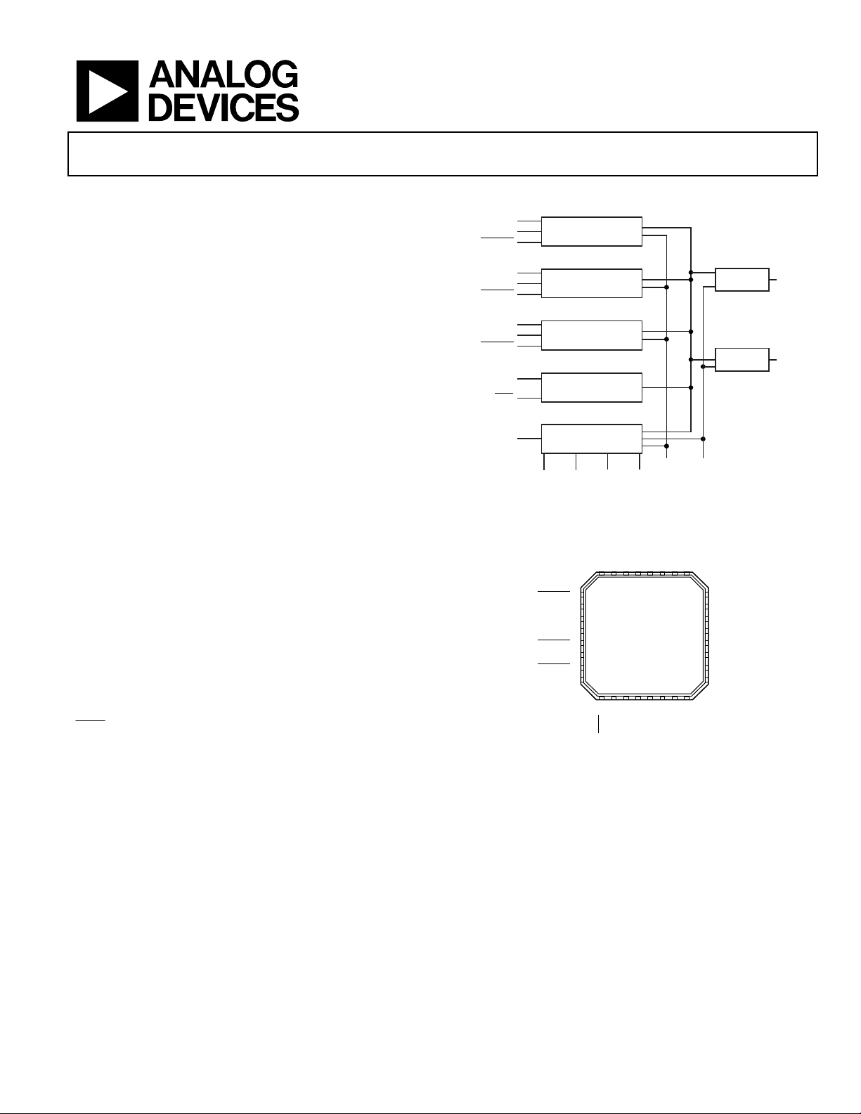
Figure 1. 4-Channel, LVDS, Laser Driver Block Diagram
Figure 2. 4-Channel, LVDS, Laser Driver Pin Configuration
For more information on the AD9665, email Analog Devices, Inc.
at
high_current_drivers.com@analog.com.
WRITE
CHANNEL 3
WRITE
CHANNEL 2
WRITE
CHANNEL 1
READ CHANNEL
OSCILLATOR
ADJ1FADJ2AADJ1AADJ2
VDDN/C
OSCEN
OUTSELF
32
31302928272625
1
W3DISN
2
W3DIS*
3
GND
4
GND
5
W2DISN
6
W2DIS*
7
W1DISN
8
W1DIS*
TTL ACTIVE LOW SEE TABLE 3
AD9665
LFCSP
5mm
×
5mm
(Not to Scale)
9
10111213141516
DD
VDDV
RDIS
W3SET
INS OUTSEL
ADJ1AADJ2
ADJ1FADJ2
A
RSET
W2SET
W1SET
ENABLE
OUTPUT A
OUTPUT B
ENABLE
24
INS
23
V
DD
22
LD1
21
LD1
20
GND
19
LD2
18
LD2
17
V
DD
05269-050
LD1
LD2
05269-001
Rev. SpD
Information furnished by Analog Devices is believed to be accurate and reliable. However, no
responsibility is assumed by Anal og Devices for its use, nor for any infringements of patents or ot her
rights of third parties that may result from its use. Specifications subject to change without notice. No
license is granted by implication or otherwise under any patent or patent rights of Analog Devices.
Trademarks and registered trademarks are the property of their respective owners.
One Technology Way, P.O. Box 9106, Norwood, MA 02062-9106, U.S.A.
Tel: 781.329.4700 www.analog.com
Fax: 781.461.3113 © 2005 Analog Devices, Inc. All rights reserved.

AD9665
© 2005 Analog Devices, Inc. All rights reserved. Trademarks and
registered trademarks are the property of their respective owners.
D05269F-0-12/05(SpD)
Rev. SpD | Page 2 of 2
 Loading...