

Quad Input Multiservice Line Card Adaptive
Data Sheet
FEATURES
Supports GR-1244 Stratum 3 stability in holdover mode
Supports smooth reference switchover with virtually
no disturbance on output phase
Supports Telcordia GR-253 jitter generation, transfer, and
tolerance for SONET/SDH up to OC-192 systems
Supports ITU-T G.8262 synchronous Ethernet slave clocks
Supports ITU-T G.823, G.824, G.825, and G.8261
Auto/manual holdover and reference switchover
4 reference inputs (single-ended or differential)
Input reference frequencies: 2 kHz to 1250 MHz
Reference validation and frequency monitoring (1 ppm)
Programmable input reference switchover priority
20-bit programmable input reference divider
6 pairs of clock output pins with each pair configurable as
a single differential LVDS/HSTL output or as 2 single-ended
CMOS outputs
Output frequencies: 352 Hz to 1250 MHz
Programmable 17-bit integer and 24-bit fractional
feedback divider in digital PLL
Programmable digital loop filter covering loop bandwidths
from 0.1 Hz to 5 kHz (2 kHz maximum for <0.1 dB of
peaking)
Low noise system clock multiplier
Frame sync support
Adaptive clocking
Optional crystal resonator for system clock input
On-chip EEPROM to store multiple power-up profiles
Clock Translator with Frame Sync
AD9558
Pin program function for easy frequency translation
configuration
Software controlled power-down
64-lead, 9 mm × 9 mm, LFCSP package
APPLICATIONS
Network synchronization, including synchronous Ethernet
and SDH to OTN mapping/demapping
Cleanup of reference clock jitter
SONET/SDH clocks up to OC-192, including FEC
Stratum 3 holdover, jitter cleanup, and phase transient
control
Wireless base station controllers
Cable infrastructure
Data communications
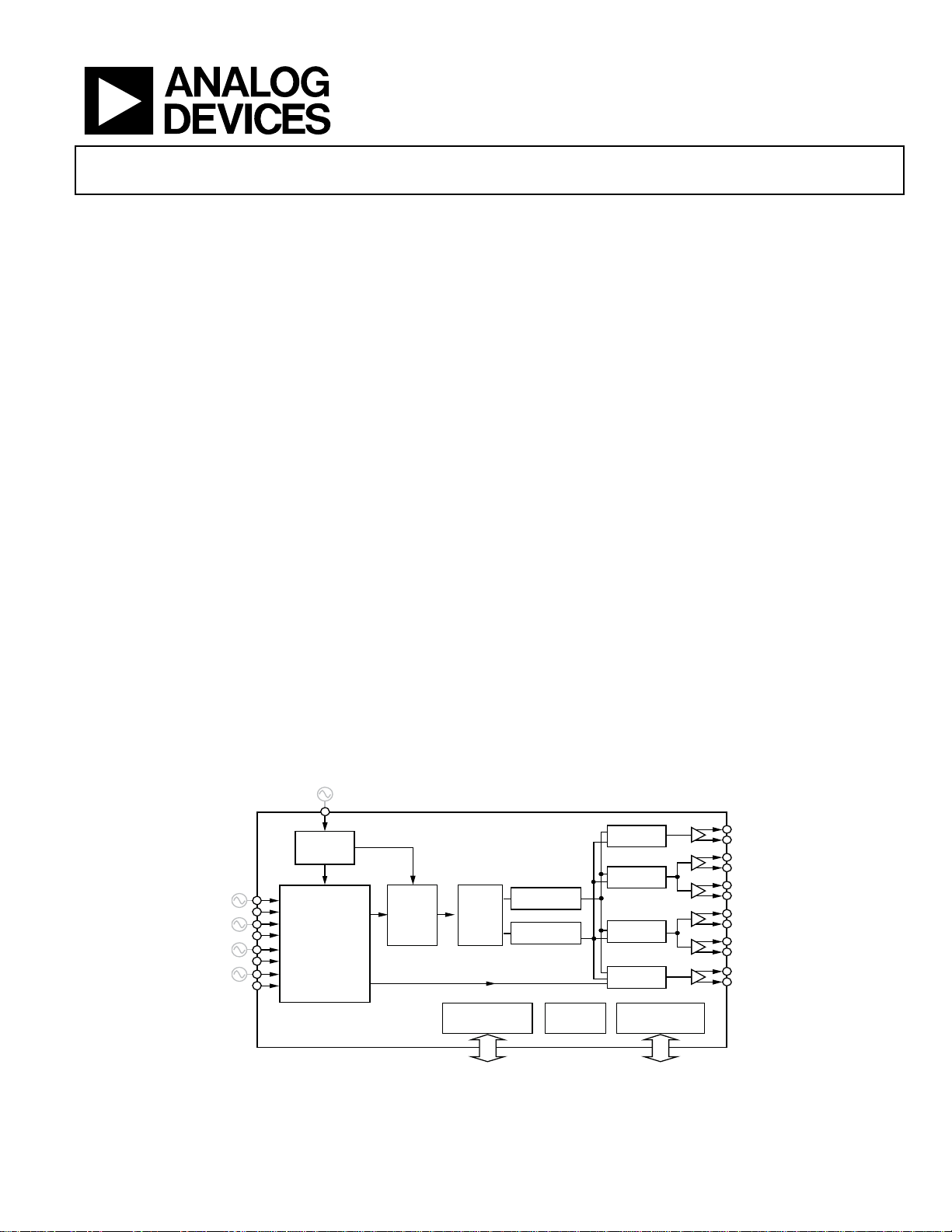
GENERAL DESCRIPTION
The AD9558 is a low loop bandwidth clock multiplier that
provides jitter cleanup and synchronization for many systems,
including synchronous optical networks (SONET/SDH). The
AD9558 generates an output clock synchronized to up to four
external input references. The digital PLL allows for reduction
of input time jitter or phase noise associated with the external
references. The digitally controlled loop and holdover circuitry
of the AD9558 continuously generates a low jitter output clock
even when all reference inputs have failed.
The AD9558 operates over an industrial temperature range of
−40°C to +85°C. If a smaller package is required, refer to the
AD9557 for the two-input/two-output version of the same part.
STABLE
FUNCTIONAL BLOCK DIAGRAM
SOURCE
CLOCK
MULTIPLIER
DIGITAL
REFERENCE INPUT
AND
MONITOR MUX
Rev. A
Information furnished by Analog Devices is believed to be accurate and reliable. However, no
responsibility is assumed by Anal og Devices for its use, nor for any infringements of patents or ot her
rights of third parties that may result from its use. Specifications subject to change without notice. No
license is granted by implication or otherwise under any patent or patent rights of Analog Devices.
Trademarks and registered trademarks are the property of their respective owners.
PLL
SERIAL I NTERFACE
AD9558
ANALOG
PLL
FRAME SYNC
(SPI OR I
Figure 1.
CHANNEL 0
DIVIDER
CHANNEL 1
÷3 TO ÷11
HF DIVIDER 0
÷3 TO ÷11
HF DIVIDER 1
2
C)
EEPROM
One Technology Way, P.O. Box 9106, Norwood, MA 02062-9106, U.S.A.
Tel: 781.329.4700 www.analog.com
Fax: 781.461.3113 ©2011–2012 Analog Devices, Inc. All rights reserved.
DIVIDER
CHANNEL 2
DIVIDER
CHANNEL 3
DIVIDER
STATUS AND
CONTROL P INS
09758-001

AD9558 Data Sheet
TABLE OF CONTENTS
Features.............................................................................................. 1
Applications....................................................................................... 1
General Description ......................................................................... 1
Functional Block Diagram .............................................................. 1
Revision History ............................................................................... 3
Specifications..................................................................................... 4
Supply Voltage............................................................................... 4
Supply Current.............................................................................. 4
Power Dissipation......................................................................... 5
Logic Inputs (
Logic Outputs (M7 to M0, IRQ) ................................................ 6
System Clock Inputs (XOA, XOB) ............................................. 6
Reference Inputs........................................................................... 7
Reference Monitors...................................................................... 8
Reference Switchover Specifications.......................................... 8
Distribution Clock Outputs........................................................ 9
Time Duration of Digital Functions........................................ 10
Digital PLL .................................................................................. 11
Digital PLL Lock Detection ...................................................... 11
Holdover Specifications............................................................. 11
Serial Port Specifications—SPI Mode...................................... 12
Serial Port Specifications—I2C Mode...................................... 13
Jitter Generation .........................................................................13
Absolute Maximum Ratings.......................................................... 16
ESD Caution................................................................................ 16
Pin Configuration and Function Descriptions........................... 17
Typical Performance Characteristics ........................................... 20
Input/Output Termination Recommendations.......................... 25
Getting Started................................................................................ 26
Chip Power Monitor and Startup............................................. 26
Multifunction Pins at Reset/Power-Up ................................... 26
Device Register Programming When Using a Register
Setup File .....................................................................................26
Register Programming Overview............................................. 26
Theory of Operation ...................................................................... 29
Overview...................................................................................... 29
Reference Clock Inputs.............................................................. 30
Reference Monitors .................................................................... 30
Reference Profiles....................................................................... 30
Reference Switchover ................................................................. 30
SYNC
RESET
,
, PINCONTROL, M7 to M0).... 5
Digital PLL (DPLL) Core .......................................................... 31
Loop Control State Machine..................................................... 34
System Clock (SYSCLK)................................................................ 35
System Clock Inputs................................................................... 35
System Clock Multiplier............................................................ 35
Output PLL (APLL) ....................................................................... 37
Clock Distribution.......................................................................... 38
Clock Dividers ............................................................................ 38
Output Power-Down ................................................................. 38
Output Enable............................................................................. 38
Output Mode .............................................................................. 38
Clock Distribution Synchronization........................................ 38
Frame Synchronization.................................................................. 40
Reference Configuration in Frame Synchronization Mode . 40
Clock Outputs in Frame Synchronization Mode................... 40
Control Registers for Frame Synchronization Mode............. 40
Level Sensitive Mode and One-Shot Mode............................. 40
Channel Divider 3/OUT5 Programming in Frame
Synchronization Mode .............................................................. 41
Status and Control.......................................................................... 42
Multifunction Pins (M7 to M0) ............................................... 42
Watchdog Timer......................................................................... 43
EEPROM ..................................................................................... 43
Serial Control Port ......................................................................... 49
SPI/IC Port Selection................................................................ 49
SPI Serial Port Operation.......................................................... 49
IC Serial Port Operation.......................................................... 53
Programming the I/O Registers ................................................... 56
Buffered/Active Registers.......................................................... 56
Autoclear Registers..................................................................... 56
Register Access Restrictions...................................................... 56
Thermal Performance.................................................................... 57
Power Supply Partitions................................................................. 58
Recommended Configuration for 3.3 V Switching Supply .. 58
Configuration for 1.8 V Supply................................................ 58
Pin Program Function Description ............................................. 59
Overview of On-Chip ROM Features ..................................... 59
Hard Pin Programming Mode.................................................. 60
Soft Pin Programming Overview............................................. 61
Register Map ................................................................................... 62
Rev. A | Page 2 of 104

Data Sheet AD9558
Register Map Bit Descriptions.......................................................72
Serial Port Configuration (Register 0x0000 to
Register 0x0005)..........................................................................72
Silicon Revision (Register 0x000A) ..........................................72
Clock Part Serial ID (Register 0x000C to Register 0x000D).72
System Clock (Register 0x0100 to Register 0x0108) ..............73
General Configuration (Register 0x0200 to
Register 0x0214)..........................................................................74
IRQ Mask (Register 0x020A to Register 0x020F)...................75
DPLL Configuration (Register 0x0300 to Register 0x032E).76
Output PLL Configuration (Register 0x0400 to
Register 0x0408)..........................................................................79
Output Clock Distribution (Register 0x0500 to
Register 0x0515)..........................................................................81
Reference Inputs (Register 0x0500 to Register 0x0507) ........85
REVISION HISTORY
4/12—Rev 0 to Rev. A
Changed 3 Hz to 352 kHz in Output Frequencies List Item,
Features Section................................................................................. 1
Change to Output Frequency Range Parameter, Min; and System
Clock Input Doubler Duty Cycle Parameter Description, Table 6... 6
Changes to Test Conditions/Comments Column, Table 9 .......... 8
Changes to Output Frequency Parameters, Min, Table 10.......... 9
Changes to Pin 4 and Pin 42, Table 20 .........................................17
Changes to Device Register Programming When Using a
Register Setup File and Register Programming Overview
Sections............................................................................................. 26
Changed APLL VCO Lower Frequency and OUT5 Frequency
Range, Figure 35; Changed 225 MHz to 200 MHz and 3.45 GHz
to 3.35 GHz in Overview Section...................................................29
Changes to Reference Profiles Section .........................................30
Changes to Programmable Digital Loop Filter Section ............. 32
Changes to System Clock Inputs Section..................................... 35
Changes to Output PLL (APLL) Section; Changes to Figure 39.... 37
Changes to Figure 40; Changed 1024 to 1023 in Clock Dividers
Section; Changes to Clock Distribution Synchronization
Section ..............................................................................................38
Changes to Multifunction Pins (M7 to M0) and IRQ Pin
Sections............................................................................................. 42
Changes to Figure 44 ......................................................................43
Changes to EEPROM Conditional Processing Section and
Figure 45............................................................................................ 46
Added Programming the EEPROM to Configure an M Pin
to Control Synchronization of Clock Distribution Section ......... 48
Changes to the Power Supply Partitions Section ........................58
Changed 89.5° to 88.5° in DPLL Phase Margin Section ............59
Changes to Address 0x0006, Address 0x0007, and
Address 0x000A, Table 35 ..............................................................62
Changes to Address 0x0304, Table 35 ..........................................63
Changes to Address 0x0405, Table 35 ..........................................64
Rev. A | Page 3 of 104
Frame Synchronization (Register 0x0640 to
Register 0x0641)..........................................................................86
DPLL Profile Registers (Register 0x0700 to
Register 0x07E6) .........................................................................87
Operational Controls (Register 0x0A00 to
Register 0x0A10).........................................................................89
Quick In/Out Frequency Soft Pin Configuration
(Register 0x0C00 to Register 0x0C08) .....................................92
Status ReadBack (Register 0x0D00 to Register 0x0D14).......93
EEPROM Control (Register 0x0E00 to Register 0x0E03).....97
EEPROM Storage Sequences (Register 0x0E10 to
Register 0x0E3C).........................................................................98
Outline Dimensions......................................................................104
Ordering Guide.........................................................................104
Changes to Address 0x071A and Address 0x071D, Table 35 ....65
Changes to Address 0x0780, Address 0x0785 to
Address 0x078A, Address 0x079A, Address 0x079D, Table 35 ...67
Changes to Address 0x07C0, Address 0x07DA, and
Address 0x07DD, Table 35 ............................................................. 68
Change to Address 0x0A01, Bit 7, Table 35................................. 69
Added Address 0x0E3D to Address 0x0E45, Table 35............... 71
Change to Table 38; Added Table 40, Renumbered Sequentially;
Changes to Table 41 ........................................................................72
Change to Bit 0, Address 0x0101, Table 43 .................................. 73
Changes to Address 0x0304, Table 55 .......................................... 76
Deleted Address 0x0305, Table 55 ................................................76
Changes to Table Title, Table 63; Changes to Address 0x0400
and Address 0x0403, Table 64........................................................ 79
Changes to Address 0x0405, Table 64 .......................................... 80
Changes to Descriptions, Address 0x0500, Table 67 ..................81
Changes to Bit 0, Address 0x0501, Table 68 ................................ 82
Changes to Bits[6:4], Address 0x0505 and Changes to
Address 0x0506, Table 70............................................................... 83
Changes to Bits[6:4] and Bit 0, Address 0x050F, Table 73......... 84
Change to Address 0x0704, Table 78; Changes to Bits[3:0] in
Address 0x0707 and Address 070A, Table 79; and Changes to
Address 0x070E, Table 82................................................................87
Changes to Address 0x0710, Table 83; and Changes to Bits[3:0],
Address 0x0714, Table 84................................................................. 88
Changes to Bits[1:0], Address 0x0A01, Table 90...........................89
Changes to Descriptions, Address 0x0A0B, Table 99................. 91
Changes to Bit 4, Address 0x0C06, Table 100 ............................. 93
Changes to Bit 6 and Bit 1, Address 0x0D01, Table 102 ............94
Changes to Table Summary, Table 114......................................... 98
Added Table 128............................................................................ 101
Changes to Table 129 ....................................................................102
Changes to Table 130 ....................................................................103
10/11—Revision 0: Initial Version

AD9558 Data Sheet
SPECIFICATIONS
Minimum (min) and maximum (max) values apply for the full range of supply voltage and operating temperature variations. Typical (typ)
values apply for AVDD3 = DVDD_I/O = 3.3 V; AVDD = DVDD
SUPPLY VOLTAGE
Table 1.
Parameter Min Typ Max Unit Test Conditions/Comments
SUPPLY VOLTAGE
DVDD3 3.135 3.30 3.465 V
DVDD 1.71 1.80 1.89 V
AVDD3 3.135 3.30 3.465 V
AVDD 1.71 1.80 1.89 V
SUPPLY CURRENT
The test conditions for the maximum (max) supply current are the same as the test conditions for the All Blocks Running parameter of
Tabl e 3. The test conditions for the typical (typ) supply current are the same as the test conditions for the Typical Configuration parameter
of Tabl e 3 .
Table 2.
Parameter Min Typ Max Unit Test Conditions/Comments
SUPPLY CURRENT FOR TYPICAL
CONFIGURATION
I
12 19 26 mA Pin 45, Pin 46, Pin 51, Pin 52, Pin 64
DVDD3
I
12 20 28 mA Pin 6, Pin 55, Pin 56
DVDD
I
50 70 92 mA Pin 25, Pin 26, Pin 31
AVDD3
I
152 230 305 mA
AVDD
SUPPLY CURRENT FOR THE ALL BLOCKS
RUNNING CONFIGURATION
I
23 34 46 mA Pin 45, Pin 46, Pin 51, Pin 52, Pin 64
DVDD3
I
11 22 32 mA Pin 6, Pin 55, Pin 56
DVDD
I
73 108 143 mA Pin 25, Pin 26, Pin 31
AVDD3
I
168 250 331 mA
AVDD
= 1.8 V; TA= 25°C, unless otherwise noted.
Typical numbers are for the typical configuration listed
in Table 3
Pin 7, Pin 10, Pin 12, Pin 17, Pin 22, Pin 29, Pin 30, Pin 35,
Pin 37, Pin 38
Maximum numbers are for all blocks running configuration
in Table 3
Pin 7, Pin 10, Pin 12, Pin 17, Pin 22, Pin 29, Pin 30, Pin 35,
Pin 37, Pin 38
Rev. A | Page 4 of 104
Data Sheet AD9558
POWER DISSIPATION
Table 3.
Parameter Min Typ Max Unit Test Conditions/Comments
POWER DISSIPATION
Typical Configuration 0.47 0.74 1.02 W
All Blocks Running 0.6 1.0 1.32 W
Full Power-Down 44 125 mW
Incremental Power Dissipation
Input Reference On/Off
Differential Without Divide-by-2 20 25 32 mW Additional current draw is in the DVDD3 domain only
Differential With Divide-by-2 26 32 40 mW Additional current draw is in the DVDD3 domain only
Single-Ended (Without Divide-by-2) 5 7 9 mW Additional current draw is in the DVDD3 domain only
Output Distribution Driver On/Off
LVDS (at 750 MHz) 12 17 22 mW Additional current draw is in the AVDD domain only
HSTL (at 750 MHz) 14 21 28 mW Additional current draw is in the AVDD domain only
1.8 V CMOS (at 250 MHz) 14 21 28 mW A single 1.8 V CMOS output with an 80 pF load
3.3 V CMOS (at 250 MHz) 18 27 36 mW A single 3.3 V CMOS output with an 80 pF load
Other Blocks On/Off
Second RF Divider 36 51 64 mW Additional current draw is in the AVDD domain only
Channel Divider Bypassed 10 17 23 mW Additional current draw is in the AVDD domain only
System clock: 49.152 MHz crystal; DPLL active;
both 19.44 MHz input references in differential mode;
one HSTL driver at 644.53125 MHz;
one 3.3 V CMOS driver at 161.1328125 MHz and 80 pF
capacitive load on CMOS output
System clock: 49.152 MHz crystal; DPLL active;
both input references in differential mode;
four HSTL drivers at 750 MHz;
four 3.3 V CMOS drivers at 250 MHz and 80 pF capacitive
load on CMOS outputs
Typical configuration with no external pull-up or pulldown resistors; about 2/3 of this power is on AVDD3
Conditions = typical configuration; table values show the
change in power due to the indicated operation
LOGIC INPUTS (SYNC, RESET, PINCONTROL, M7 TO M0)
Table 4.
Parameter Min Typ Max Unit Test Conditions/Comments
LOGIC INPUTS (SYNC, RESET, PINCONTROL)
Input High Voltage (VIH) 2.1 V
Input Low Voltage (VIL) 0.8 V
Input Current (I
, I
) ±50 ±100 µA
INH
INL
Input Capacitance (CIN) 3 pF
LOGIC INPUTS (M7 to M0)
Input High Voltage (VIH) 2.5 V
Input ½ Level Voltage (VIM) 1.0 2.2 V
Input Low Voltage (VIL) 0.6 V
Input Current (I
, I
) ±60 ±100 µA
INH
INL
Input Capacitance (CIN) 3 pF
Rev. A | Page 5 of 104

AD9558 Data Sheet
LOGIC OUTPUTS (M7 TO M0, IRQ)
Table 5.
Parameter Min Typ Max Unit Test Conditions/Comments
LOGIC OUTPUTS (M7 to M0, IRQ)
Output High Voltage (VOH) DVDD3 − 0.4 V IOH = 1 mA
Output Low Voltage (VOL) 0.4 V IOL = 1 mA
IRQ Leakage Current Open-drain mode
Active Low Output Mode −200 A VOH = 3.3 V
Active High Output Mode 100 A VOL = 0 V
SYSTEM CLOCK INPUTS (XOA, XOB)
Table 6.
Parameter Min Typ Max Unit Test Conditions/Comments
SYSTEM CLOCK MULTIPLIER
Output Frequency Range 750 805 MHz
Phase Frequency Detector (PFD) Rate 150 MHz
Frequency Multiplication Range 2 255
SYSTEM CLOCK REFERENCE INPUT PATH
Input Frequency Range 10 600 MHz
Minimum Input Slew Rate 20 V/s
Common-Mode Voltage 1.05 1.16 1.25 V Internally generated
Differential Input Voltage Sensitivity 250 mV p-p
System Clock Input Doubler Duty Cycle
System Clock Input = 50 MHz 45 50 55 %
System Clock Input = 20 MHz 46 50 54 %
System Clock Input = 16 MHz to 20 MHz 47 50 53 %
Input Capacitance 3 pF Single-ended, each pin
Input Resistance 4.2 kΩ
CRYSTAL RESONATOR PATH
Crystal Resonator Frequency Range 10 50 MHz Fundamental mode, AT cut crystal
Maximum Crystal Motional Resistance 100 Ω
The VCO range may place limitations on
nonstandard system clock input
frequencies
Assumes valid system clock and PFD
rates
Minimum limit imposed for jitter
performance
Minimum voltage across pins required
to ensure switching between logic
states; the instantaneous voltage on
either pin must not exceed the supply
rails; can accommodate single-ended
input by ac grounding of complementary
input; 1 V p-p recommended for optimal
jitter performance
This is the amount of duty cycle
variation that can be tolerated on the
system clock input to use the doubler
Rev. A | Page 6 of 104

Data Sheet AD9558
REFERENCE INPUTS
Table 7.
Parameter Min Typ Max Unit Test Conditions/Comments
DIFFERENTIAL OPERATION
Frequency Range
Sinusoidal Input 10 750 MHz
LVPECL Input 0.002 1250 MHz
LVDS Input 0.002 750 MHz
Minimum Input Slew Rate 40 V/s Minimum limit imposed for jitter performance
Common-Mode Input Voltage
AC-Coupled 1.9 2 2.2 V Internally generated
DC-Coupled 1.0 2.4 V
Differential Input Voltage Sensitivity mV
fIN < 800 MHz 240 mV
fIN = 800 to 1050 MHz 320 mV
fIN = 1050 to 1250 MHz 400 mV
Differential Input Voltage Hysteresis 58 100 mV
Input Resistance 21 kΩ
Input Capacitance 3 pF
Minimum Pulse Width High
LVPECL 390 ps
LVDS 640 ps
Minimum Pulse Width Low
LVPECL 390 ps
LVDS 640 ps
SINGLE-ENDED OPERATION
Frequency Range (CMOS) 0.002 300 MHz
Minimum Input Slew Rate 40 V/s Minimum limit imposed for jitter performance
Input Voltage High (VIH)
1.2 V to 1.5 V Threshold Setting 1.0 V
1.8 V to 2.5 V Threshold Setting 1.4 V
3.0 V to 3.3 V Threshold Setting 2.0 V
Input Voltage Low (VIL)
1.2 V to 1.5 V Threshold Setting 0.35 V
1.8 V to 2.5 V Threshold Setting 0.5 V
3.0 V to 3.3 V Threshold Setting 1.0 V
Input Resistance 47 kΩ
Input Capacitance 3 pF
Minimum Pulse Width High 1.5 ns
Minimum Pulse Width Low 1.5 ns
The reference input divide-by-2 block must be
engaged for fIN > 705 MHz
The reference input divide-by-2 block must be
engaged for f
Minimum differential voltage across pins is required to
ensure switching between logic levels; instantaneous
voltage on either pin must not exceed the supply rails
> 705 MHz
IN
Rev. A | Page 7 of 104

AD9558 Data Sheet
REFERENCE MONITORS
Table 8.
Parameter Min Typ Max Unit Test Conditions/Comments
REFERENCE MONITORS
Reference Monitor
Loss of Reference Detection Time 1.1
DPLL PFD
Nominal phase detector period = R/f
period
Frequency Out-of-Range Limits <2 105
∆f/f
REF
(ppm)
Programmable (lower bound is subject to quality
of the system clock (SYSCLK)); SYSCLK accuracy
must be better than the lower bound
Validation Timer 0.001 65.535 sec Programmable in 1 ms increments
1
f
is the frequency of the active reference; R is the frequency division factor determined by the R-divider.
REF
REFERENCE SWITCHOVER SPECIFICATIONS
Table 9.
Parameter Min Typ Max Unit Test Conditions/Comments
REFERENCE SWITCHOVER SPECIFICATIONS
Maximum Output Phase Perturbation
(Phase Build-Out Switchover)
50 Hz DPLL Loop Bandwidth Valid for automatic and manual reference switching
Peak 0 ±100 ps
Steady State 0 ±100 ps
2 kHz DPLL Loop Bandwidth Valid for automatic and manual reference switching
Peak 0 ±250 ps
Steady State 0 ±100 ps
Time Required to Switch to
a New Reference
Phase Build-Out Switchover 1.1
Assumes a jitter-free reference; satisfies Telcordia
GR-1244-CORE requirements; select high PM base
loop filter bit (Register 0x070E, Bit 0) is set to 1 for
all active references
DPLL PFD
period
Calculated using the nominal phase detector
period (NPDP = R/f
equal to the time plus the reference validation
time and the time required to lock to the new
reference
); the total time required is
REF
REF
1
Rev. A | Page 8 of 104

Data Sheet AD9558
DISTRIBUTION CLOCK OUTPUTS
Table 10.
Parameter Min Typ Max Unit Test Conditions/Comments
HSTL MODE
Output Frequency 0.000352 1250 MHz
Rise/Fall Time (20% to 80%)1 140 250 ps 100 Ω termination across output pins
Duty Cycle
Up to f
Up to f
Up to f
= 700 MHz 45 48 52 %
OUT
= 750 MHz 42 48 53 %
OUT
= 1250 MHz 43 %
OUT
Differential Output Voltage Swing 700 950 1200 mV Magnitude of voltage across pins; output driver static
Common-Mode Output Voltage 700 870 960 mV Output driver static
LVDS MODE
Output Frequency 0.000352 1250 MHz
Rise/Fall Time (20% to 80%)1 185 280 ps 100 Ω termination across the output pair
Duty Cycle
Up to f
Up to f
Up to f
= 750 MHz 44 48 53 %
OUT
= 800 MHz 43 47 53 %
OUT
= 1250 MHz 43 %
OUT
Differential Output Voltage Swing
Balanced, VOD 247 454 mV
Unbalanced, ∆VOD 50 mV
Offset Voltage
Common-Mode, VOS 1.125 1.26 1.375 V Output driver static
Common-Mode Difference, ∆VOS 50 mV Voltage difference between pins; output driver static
Short-Circuit Output Current 13 24 mA Output driver static
CMOS MODE
Output Frequency
1.8 V Supply 0.000352 150 MHz 10 pF load
3.3 V Supply (OUT0 and OUT5)
Strong Drive Strength Setting 0.000352 250 MHz 10 pF load
Weak Drive Strength Setting 0.000352 25 MHz 10 pF load
Rise/Fall Time (20% to 80%)1
1.8 V Supply 1.5 3 ns 10 pF load
3.3 V Supply
Strong Drive Strength Setting 0.4 0.6 ns 10 pF load
Weak Drive Strength Setting 8 ns 10 pF load
Duty Cycle
1.8 V Mode 50 % 10 pF load
3.3 V Strong Mode 47 % 10 pF load
3.3 V Weak Mode 51 % 10 pF load
Output Voltage High (VOH) Output driver static; strong drive strength
AVDD3 = 3.3 V, IOH = 10 mA AVDD3 − 0.3 V
AVDD3 = 3.3 V, IOH = 1 mA AVDD3 − 0.1 V
AVDD3 = 1.8 V, IOH = 1 mA AVDD − 0.2 V
Output Voltage Low (VOL) Output driver static; strong drive strength
AVDD3 = 3.3 V, IOL = 10 mA 0.3 V
AVDD3 = 3.3 V, IOL = 1 mA 0.1 V
AVDD3 = 1.8 V, IOL = 1 mA 0.1 V
OUT5 only; OUT0 to OUT4 minimum output
frequency is 360 kHz
OUT5 only; OUT0 to OUT4 minimum output
frequency is 360 kHz
Voltage swing between output pins; output driver
static
Absolute difference between voltage swing of
normal pin and inverted pin; output driver static
OUT5 only; OUT0 to OUT4 minimum output
frequency is 360 kHz
Rev. A | Page 9 of 104

AD9558 Data Sheet
Parameter Min Typ Max Unit Test Conditions/Comments
OUTPUT TIMING SKEW 10 pF load
Between OUT0 and OUT1 10 70 ps
Between OUT0 and OUT3 105 222 ps
Between OUT0 and OUT5 1.39 1.76 ns
Between OUT1 and OUT2
1 12 ps
(OUT1 and OUT2 Share the
Same Divider)
Between OUT3 and OUT4
1 24 ps
(OUT3 and OUT4 Share the
Same Divider)
Across All OUT0 to OUT4 HSTL 105 235 ps
Across All OUT0 to OUT4 LVDS 100 235 ps
Additional Delay on One Driver by
Changing Its Logic Type
HSTL to LVDS −5 +1 +5 ps
HSTL to 1.8 V CMOS −5 0 +5 ps
HSTL to 3.3 V CMOS, Strong Mode The CMOS edge is delayed relative to HSTL
OUT0 CMOS to OUT1 HSTL 3.53 3.59 ns
OUT0 CMOS to OUT3 HSTL 3.55 3.65 ns
OUT0 CMOS to OUT4 HSTL 3.56 3.68 ns
OUT0 CMOS to OUT5 HSTL 4.84 5.1 ns
1
The listed values are for the slower edge (rise or fall).
HSTL mode on both drivers; rising edge only; any
divide value
HSTL mode on both drivers; rising edge only; any
divide value
HSTL mode on both drivers; rising edge only; any
divide value
HSTL mode on both drivers; rising edge only; any
divide value
HSTL mode on both drivers; rising edge only; any
divide value
HSTL mode on all drivers; rising edge only; any
divide value
LVDS mode on all drivers; rising edge only; any
divide value
Positive value indicates that the LVDS edge is
delayed relative to HSTL
Positive value indicates that the CMOS edge is
delayed relative to HSTL
TIME DURATION OF DIGITAL FUNCTIONS
Table 11.
Parameter Min Typ Max Unit Test Conditions/Comments
TIME DURATION OF DIGITAL
FUNCTIONS
EEPROM-to-Register Download
Time
Register-to-EEPROM Upload Time 138 145 ms
Minimum Power-Down Exit Time 1 ms
13 20 ms
Using default EEPROM storage sequence
(see Register 0x0E10 to Register 0x0E3F)
Using default EEPROM storage sequence
(see Register 0x0E10 to Register 0x0E3F)
Time from power-down exit to system clock
lock detect
Rev. A | Page 10 of 104
Data Sheet AD9558
DIGITAL PLL
Table 12.
Parameter Min Typ Max Unit Test Conditions/Comments
DIGITAL PLL
Phase-Frequency Detector (PFD)
Input Frequency Range
Loop Bandwidth 0.1 2000 Hz Programmable design parameter
Phase Margin 30 89 Degrees Programmable design parameter
Closed-Loop Peaking <0.1 dB
Reference Input (R) Division Factor 1 220 1, 2, …, 1,048,576
Integer Feedback (N1) Division Factor 180 217 180, 181, …, 131,072
Fractional Feedback Divide Ratio 0 0.999 Maximum value: 16,777,215/16,777,216
DIGITAL PLL LOCK DETECTION
Table 13.
Parameter Min Typ Max Unit Test Conditions/Comments
PHASE LOCK DETECTOR
Threshold Programming Range 0.001 65.5 ns
Threshold Resolution 1 ps
FREQUENCY LOCK DETECTOR
Threshold Programming Range 0.001 16,700 ns Reference-to-feedback period difference
Threshold Resolution 1 ps
2 100 kHz
Programmable design parameter ;
part can be programmed for <0.1 dB peaking in
accordance with Telcordia GR-253 jitter transfer
HOLDOVER SPECIFICATIONS
Table 14.
Parameter Min Typ Max Unit Test Conditions/Comments
HOLDOVER SPECIFICATIONS
Initial Frequency Accuracy <0.01 ppm
Excludes frequency drift of SYSCLK source;
excludes frequency drift of input reference prior
to entering holdover; compliant with GR-1244
Stratum 3
Rev. A | Page 11 of 104

AD9558 Data Sheet
SERIAL PORT SPECIFICATIONS—SPI MODE
Table 15.
Parameter Min Typ Max Unit Test Conditions/Comments
CS
Input Logic 1 Voltage 2.0 V
Input Logic 0 Voltage 0.8 V
Input Logic 1 Current 60 µA
Input Logic 0 Current 100 µA
Input Capacitance 2 pF
SCLK Internal 30 kΩ pull-down resistor
Input Logic 1 Voltage 2.0 V
Input Logic 0 Voltage 0.8 V
Input Logic 1 Current 200 µA
Input Logic 0 Current 1 µA
Input Capacitance 2 pF
SDIO
As an Input
Input Logic 1 Voltage 2.0 V
Input Logic 0 Voltage 0.8 V
Input Logic 1 Current 1 µA
Input Logic 0 Current 1 µA
Input Capacitance 2 pF
As an Output
Output Logic 1 Voltage DVDD3 − 0.6 V 1 mA load current
Output Logic 0 Voltage 0.4 V 1 mA load current
SDO
Output Logic 1 Voltage DVDD3 − 0.6 V 1 mA load current
Output Logic 0 Voltage 0.4 V 1 mA load current
TIMING
SCLK
Clock Rate, 1/t
Pulse Width High, t
Pulse Width Low, t
40 MHz
CLK
10 ns
HIGH
13 ns
LOW
SDIO to SCLK Setup, tDS 3 ns
SCLK to SDIO Hold, tDH 6 ns
SCLK to Valid SDIO and SDO, tDV 10 ns
CS to SCLK Setup (tS)
CS to SCLK Hold (tC)
CS Minimum Pulse Width High
10 ns
0 ns
6 ns
Rev. A | Page 12 of 104

Data Sheet AD9558
SERIAL PORT SPECIFICATIONS—I2C MODE
Table 16.
Parameter Min Typ Max Unit Test Conditions/Comments
SDA, SCL (AS INPUT)
Input Logic 1 Voltage
0.7 ×
DVDD3
Input Logic 0 Voltage
Input Current −10 +10 µA For VIN = 10% to 90% DVDD3
Hysteresis of Schmitt Trigger Inputs
0.015 ×
DVDD3
Pulse Width of Spikes That Must Be Suppressed by
the Input Filter, t
SP
50 ns
SDA (AS OUTPUT)
Output Logic 0 Voltage 0.4 V IO = 3 mA
Output Fall Time from V
IHmin
to V
ILmax
20 + 0.1
1
C
b
TIMING
SCL Clock Rate 400 kHz
Bus-Free Time Between a Stop and Start
Condition, t
BUF
Repeated Start Condition Setup Time, t
Repeated Hold Time Start Condition, t
Stop Condition Setup Time, t
Low Period of the SCL Clock, t
SU; STO
LOW
High Period of the SCL Clock, t
SCL/SDA Rise Time, t
R
HD; STA
0.6 µs
1.3 µs
0.6 µs
HIGH
SU; STA
0.6 µs
1.3 µs
0.6 µs
20 + 0.1 C
SCL/SDA Fall Time, tF 20 + 0.1 C
Data Setup Time, t
Data Hold Time, t
Capacitive Load for Each Bus Line, C
1
Cb is the capacitance (pF) of a single bus line.
100 ns
SU; DAT
100 ns
HD; DAT
1
400 pF
b
V
0.3 ×
V
DVDD3
250 ns 10 pF ≤ Cb ≤ 400 pF
After this period, the first clock pulse is
generated
1
300 ns
b
1
300 ns
b
JITTER GENERATION
Jitter generation (random jitter) uses 49.152 MHz crystal for system clock input.
Table 17.
Parameter Min Typ Max Unit Test Conditions/Comments
JITTER GENERATION
f
= 19.44 MHz; f
REF
= 622.08 MHz; f
OUT
LOOP
= 50 Hz
HSTL Driver
Bandwidth: 5 kHz to 20 MHz 304 fs rms
Bandwidth: 12 kHz to 20 MHz 296 fs rms
Bandwidth: 20 kHz to 80 MHz 300 fs rms
Bandwidth: 50 kHz to 80 MHz 266 fs rms
Bandwidth: 16 MHz to 320 MHz 185 fs rms
Rev. A | Page 13 of 104
System clock doubler enabled;
high phase margin mode enabled;
Register 0x0405 = 0x20; Register 0x0403 =
0x07; Register 0x0400 = 0x81;
in cases where multiple driver types are
listed, both driver types were tested at
those conditions, and the one with higher
jitter is quoted, although there is usually
not a significant jitter difference between
the driver types

AD9558 Data Sheet
Parameter Min Typ Max Unit Test Conditions/Comments
f
= 19.44 MHz; f
REF
= 644.53 MHz; f
OUT
LOOP
= 50 Hz
HSTL and/or LVDS Driver
Bandwidth: 5 kHz to 20 MHz 334 fs rms
Bandwidth: 12 kHz to 20 MHz 321 fs rms
Bandwidth: 20 kHz to 80 MHz 319 fs rms
Bandwidth: 50 kHz to 80 MHz 277 fs rms
Bandwidth: 16 MHz to 320 MHz 185 fs rms
f
= 19.44 MHz; f
REF
= 693.48 MHz; f
OUT
LOOP
= 50 Hz
HSTL Driver
Bandwidth: 5 kHz to 20 MHz 298 fs rms
Bandwidth: 12 kHz to 20 MHz 285 fs rms
Bandwidth: 20 kHz to 80 MHz 286 fs rms
Bandwidth: 50 kHz to 80 MHz 252 fs rms
Bandwidth: 16 MHz to 320 MHz 183 fs rms
f
= 19.44 MHz; f
REF
= 174.703 MHz; f
OUT
LOOP
= 1 kHz
HSTL Driver
Bandwidth: 5 kHz to 20 MHz 354 fs rms
Bandwidth: 12 kHz to 20 MHz 301 fs rms
Bandwidth: 20 kHz to 80 MHz 321 fs rms
Bandwidth: 50 kHz to 80 MHz 290 fs rms
Bandwidth: 4 MHz to 80 MHz 177 fs rms
f
= 19.44 MHz; f
REF
= 174.703 MHz; f
OUT
= 100 Hz
LOOP
LVDS and/or 3.3 V CMOS Driver
Bandwidth: 5 kHz to 20 MHz 306 fs rms
Bandwidth: 12 kHz to 20 MHz 293 fs rms
Bandwidth: 20 kHz to 80 MHz 313 fs rms
Bandwidth: 50 kHz to 80 MHz 283 fs rms
Bandwidth: 4 MHz to 80 MHz 166 fs rms
f
= 25 MHz; f
REF
= 161.1328 MHz; f
OUT
= 100 Hz
LOOP
HSTL Driver
Bandwidth: 5 kHz to 20 MHz 316 fs rms
Bandwidth: 12 kHz to 20 MHz 302 fs rms
Bandwidth: 20 kHz to 80 MHz 324 fs rms
Bandwidth: 50 kHz to 80 MHz 292 fs rms
Bandwidth: 4 MHz to 80 MHz 171 fs rms
f
= 2 kHz; f
REF
= 70.656 MHz; f
OUT
= 100 Hz;
LOOP
HSTL and/or 3.3 V CMOS Driver
Bandwidth: 10 Hz to 30 MHz 3.22
Bandwidth: 5 kHz to 20 MHz 338 fs rms
Bandwidth: 12 kHz to 20 MHz 324 fs rms
Bandwidth: 10 kHz to 400 kHz 278 fs rms
Bandwidth: 100 kHz to 10 MHz 210 fs rms
f
= 25 MHz; f
REF
= 1 GHz; f
OUT
= 500 Hz
LOOP
HSTL Driver
Bandwidth: 100 Hz to 500 MHz (Broadband) 1.71
Bandwidth: 12 kHz to 20 MHz 343 fs rms
Bandwidth: 20 kHz to 80 MHz 338 fs rms
ps
rms
ps
rms
Rev. A | Page 14 of 104

Data Sheet AD9558
Jitter generation (random jitter) uses 19.2 MHz TCXO for system clock input.
Table 18.
Parameter Min Typ Max Unit Test Conditions/Comments
JITTER GENERATION
f
= 19.44 MHz; f
REF
= 644.53 MHz; f
OUT
= 0.1 Hz
LOOP
HSTL Driver
Bandwidth: 5 kHz to 20 MHz 402 fs rms
Bandwidth: 12 kHz to 20 MHz 393 fs rms
Bandwidth: 20 kHz to 80 MHz 391 fs rms
Bandwidth: 50 kHz to 80 MHz 347 fs rms
Bandwidth: 16 MHz to 320 MHz 179 fs rms
f
= 19.44 MHz; f
REF
= 693.48 MHz; f
OUT
= 0.1 Hz
LOOP
HSTL Driver
Bandwidth: 5 kHz to 20 MHz 379 fs rms
Bandwidth: 12 kHz to 20 MHz 371 fs rms
Bandwidth: 20 kHz to 80 MHz 371 fs rms
Bandwidth: 50 kHz to 80 MHz 335 fs rms
Bandwidth: 16 MHz to 320 MHz 175 fs rms
f
= 19.44 MHz; f
REF
= 312.5 MHz; f
OUT
= 0.1 Hz
LOOP
HSTL Driver
Bandwidth: 5 kHz to 20 MHz 413 fs rms
Bandwidth: 12 kHz to 20 MHz 404 fs rms
Bandwidth: 20 kHz to 80 MHz 407 fs rms
Bandwidth: 50 kHz to 80 MHz 358 fs rms
Bandwidth: 4 MHz to 80 MHz 142 fs rms
f
= 25 MHz; f
REF
= 161.1328 MHz; f
OUT
LOOP
= 0.1 Hz
HSTL Driver
Bandwidth: 5 kHz to 20 MHz 399 fs rms
Bandwidth: 12 kHz to 20 MHz 391 fs rms
Bandwidth: 20 kHz to 80 MHz 414 fs rms
Bandwidth: 50 kHz to 80 MHz 376 fs rms
Bandwidth: 4 MHz to 80 MHz 190 fs rms
f
= 2 kHz; f
REF
= 70.656 MHz; f
OUT
= 0.1 Hz
LOOP
HSTL and/or 3.3 V CMOS Driver
Bandwidth: 10 Hz to 30 MHz 970 fs rms
Bandwidth: 12 kHz to 20 MHz 404 fs rms
Bandwidth: 10 kHz to 400 kHz 374 fs rms
Bandwidth: 100 kHz to 10 MHz 281 fs rms
System clock doubler enabled; high phase
margin mode enabled; Register 0x0405 = 0x20;
Register 0x0403 = 0x07; Register 0x0400 = 0x81;
in cases where multiple driver types are listed,
both driver types were tested at those conditions,
and the one with higher jitter is quoted, although
there is usually not a significant jitter difference
between the driver types
Rev. A | Page 15 of 104
AD9558 Data Sheet
ABSOLUTE MAXIMUM RATINGS
Table 19.
Parameter Rating
Analog Supply Voltage (AVDD) 2 V
Digital Supply Voltage (DVDD) 2 V
Digital I/O Supply Voltage (DVDD3) 3.6 V
Analog Supply Voltage (AVDD3) 3.6 V
Maximum Digital Input Voltage −0.5 V to DVDD3 + 0.5 V
Storage Temperature Range −65°C to +150°C
Operating Temperature Range −40°C to +85°C
Lead Temperature
(Soldering 10 sec)
Junction Temperature 150°C
300°C
Stresses above those listed under Absolute Maximum Ratings
may cause permanent damage to the device. This is a stress
rating only; functional operation of the device at these or any
other conditions above those indicated in the operational
section of this specification is not implied. Exposure to absolute
maximum rating conditions for extended periods may affect
device reliability.
ESD CAUTION
Rev. A | Page 16 of 104
Data Sheet AD9558
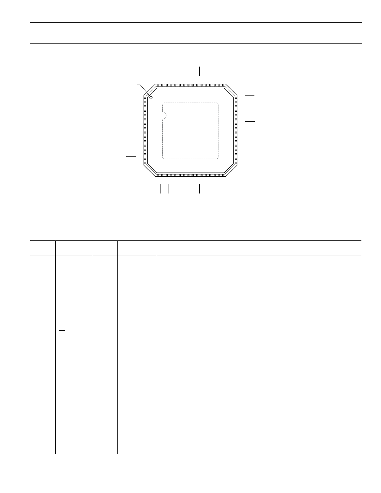
PIN CONFIGURATION AND FUNCTION DESCRIPTIONS
DVDD3M6M5M4M3M2M1M0DVDD
PIN 1
INDICATOR
IRQ
SDO
CS
DVDD
AVD D
XOA
XOB
AVD D
NC
AVD D
OUT4
OUT4
OUT3
OUT3
1
2
3
4
5
6
7
8
9
10
11
12
13
14
15
16
SCLK/SCL
SDIO/SDA
NOTES
1. NC = NO CONNECT. DO NOT CONNECT TO THIS PIN.
2. THE EXPOSED PAD MUST BE CONNECTED TO GROUND (VSS).
646362616059585756555453525150
(Not to Scale)
171819202122232425262728293031
OUT2
OUT2
OUT1
OUT1
AVD D
AD9558
TOP VIEW
OUT5
OUT5
AVD D
AVD D3
DVDD
REFB
REFB
DVDD3
DVDD3
REFD
REFD
49
48
REFC
47
REFC
46
DVDD3
45
DVDD3
44
REFA
43
REFA
42
SYNC
41
M7
40
PINCONTROL
39
RESET
38
AVD D
37
AVD D
36
NC
35
AVD D
34
NC
33
LF_VCO2
32
OUT0
OUT0
AVD D
AVD D
AVD D3
AVD D3
LDO_VCO2
Figure 2. Pin Configuration
Table 20. Pin Function Descriptions
Input/
Pin No. Mnemonic
Output
Pin Type Description
1 IRQ O 3.3 V CMOS Interrupt Request Line.
2 SCLK/SCL I 3.3 V CMOS
Serial Programming Clock (SCLK) in SPI Mode. Data clock for serial programming.
Open-Collector Serial Clock Pin (SCL) in I
2
C Mode. Requires a pull-up resistor, usually
2.2 kΩ; the resistor size depends on the number of I
3 SDIO/SDA I/O 3.3 V CMOS
Serial Data Input/Output (SDIO) in SPI Mode. When the device is in 4-wire SPI mode,
data is written via this pin. In 3-wire SPI mode, both data reads and writes occur on
this pin. There is no internal pull-up/pull-down resistor on this pin.
Open-Collector Serial Data Pin (SDA) in I2C Mode. Requires a pull-up resistor, usually
2.2 kΩ; the resistor size depends on the number of I
4 SDO O 3.3 V CMOS
Serial Data Output. Use this pin to read data in 4-wire mode. There is no internal pull-up/
pull-down resistor on this pin. This pin is high impedance in the default 3-wire mode.
5
CS
I 3.3 V CMOS
Chip Select (SPI), Active Low. When programming a device, this pin must be held low.
In systems where more than one AD9558 is present, this pin enables individual
programming of each AD9558. This pin has an internal 10 kΩ pull-up resistor.
6, 55, 56 DVDD I Power 1.8 V Digital Supply.
7 AVDD I Power 1.8 V Analog (SYSCLK) Power Supply.
8 XOA I
Differential
input
System Clock Input. XOA contains internal dc biasing and should be ac-coupled with
a 0.01 F capacitor, except when using a crystal. If a crystal is used, connect the crystal
across XOA and XOB. Single-ended 1.8 V CMOS is also an option but can introduce
a spur if the duty cycle is not 50%. When using XOA as a single-ended input, connect
a 0.01 F capacitor from XOB to ground.
9 XOB I
Differential
input
Complementary System Clock Input. Complementary signal to XOA. XOB contains
internal dc biasing and should be ac-coupled with a 0.01 F capacitor, except when
using a crystal. If a crystal is used, connect the crystal across XOA and XOB.
10 AVDD I Power 1.8 V Analog (VCO) Power Supply.
11 NC I No Connection. Do not connect to this pin.
12, 17,
AVDD I Power 1.8 V Analog (Output Driver) Power Supply.
22, 29,
30
09758-002
2
C devices on the bus.
2
C devices on the bus.
Rev. A | Page 17 of 104
AD9558 Data Sheet
Input/
Pin No. Mnemonic
13
14 OUT4 O
15
16 OUT3 O
18
19 OUT2 O
20
21 OUT1 O
23
24 OUT5 O
25, 26 AVDD3 I Power 3.3 V Analog (Output Driver) Power Supply.
27
28 OUT0 O
31 AVDD3 I Power 3.3V Analog (VCO 2) Power Supply.
32 LDO_VCO2 I LDO bypass
33 LF_VCO2 I/O Loop filter
34 NC No Connect. There is no internal connection for this pin.
35 AVDD I Power 1.8 V Analog (APLL) Power Supply.
36 NC No Connect. There is no internal connection for this pin.
37, 38 AVDD I Power 1.8 V Analog (DCO and TDC) Power Supplies.
39
40 PINCONTROL I 3.3 V CMOS
41 M7 I/O 3.3 V CMOS
42
OUT4
OUT3
OUT2
OUT1
OUT5
OUT0
RESET
SYNC
Output Pin Type Description
O
O
O
O
O
O
I 3.3 V CMOS
I 3.3 V CMOS
HSTL, LVDS, or
1.8 V CMOS
HSTL, LVDS,
or 1.8 V CMOS
HSTL, LVDS, or
1.8 V CMOS
HSTL, LVDS, or
1.8 V CMOS
HSTL, LVDS, or
1.8 V CMOS
HSTL, LVDS, or
1.8 V CMOS
HSTL, LVDS, or
1.8 V CMOS
HSTL, LVDS,
or 1.8 V CMOS
HSTL, LVDS,
1.8 V CMOS,
3.3 V CMOS
HSTL, LVDS,
1.8 V CMOS,
3.3 V CMOS
HSTL, LVDS,
1.8 V CMOS,
3.3 V CMOS
HSTL, LVDS,
1.8 V CMOS,
3.3 V CMOS
Complementary Output 4. This output can be configured as HSTL, LVDS, or single-ended
1.8 V CMOS.
Output 4. This output can be configured as HSTL, LVDS, or single-ended 1.8 V CMOS.
LVPECL levels can be achieved by ac coupling and using the Thevenin-equivalent
termination as described in the Input/Output Termination Recommendations section.
Complementary Output 3. This output can be configured as HSTL, LVDS,
or single-ended 1.8 V CMOS.
Output 3. This output can be configured as HSTL, LVDS, or single-ended 1.8 V CMOS.
LVPECL levels can be achieved by ac coupling and using the Thevenin-equivalent
termination as described in the Input/Output Termination Recommendations section.
Complementary Output 2. This output can be configured as HSTL, LVDS, or
single-ended 1.8 V CMOS.
Output 2. This output can be HSTL, LVDS, or single-ended 1.8 V CMOS.
LVPECL levels can be achieved by ac coupling and using the Thevenin-equivalent
termination as described in the Input/Output Termination Recommendations section.
Complementary Output 1. This output can be configured as HSTL, LVDS, or
single-ended 1.8 V CMOS.
Output 1. This output can be configured as HSTL, LVDS, or single-ended 1.8 V CMOS.
LVPECL levels can be achieved by ac coupling and using the Thevenin-equivalent
termination as described in the Input/Output Termination Recommendations section.
Complementary Output 5. This output can be configured as HSTL, LVDS, or single-ended
1.8 V or 3.3 V CMOS.
Output 5. This output can be configured as HSTL, LVDS, or single-ended 1.8 V or 3.3 V
CMOS. LVPECL levels can be achieved by ac coupling and by using the Theveninequivalent termination as described in the Input/Output Termination
Recommendations section.
Complementary Output 0. This output can be configured as HSTL, LVDS, or singleended 1.8 V or 3.3 V CMOS.
Output 0. This output can be configured as HSTL, LVDS, or single-ended 1.8 V or 3.3 V
CMOS. LVPECL levels can be achieved by ac coupling and by using the Theveninequivalent termination as described in the Input/Output Termination
Recommendations section.
Output PLL Loop Filter Voltage Regulator. Connect a 0.47 F capacitor from this pin
to ground. This pin is also the ac ground reference for the integrated output PLL
external loop filter.
Loop Filter Node for the Output PLL. Connect an external 6.8 nF capacitor from this
pin to Pin 32 (LDO_VCO2).
Chip Reset. When this active low pin is asserted, the chip goes into reset. This pin has
an internal 50 kΩ pull-up resistor.
Pin Program Mode Enable Pin. When pulled high during startup, this pin enables pin
programming of the AD9558 configuration during startup. If this pin is low during
startup, the user must program the part via the serial port, or use values that are
stored in the EEPROM.
Configurable I/O Pin. Along with pins M6 through M0, this pin is configured through
the AD9558 register space.
Clock Distribution Synchronization Pin. When this pin is activated, output drivers are
held static and then synchronized on a low-to-high transition of this pin. This pin is
used to arm the frame sync function when frame sync mode is enabled and has an
internal 60 kΩ pull-up resistor.
Rev. A | Page 18 of 104

Data Sheet AD9558
Input/
Pin No. Mnemonic
43 REFA I
44
45, 46,
51, 52
47 REFC I
48
49 REFD I
50
53 REFB I
54
57, 58,
59, 60,
61, 62,
63
64 DVDD3 I Power 3.3 V Digital Supply.
EP VSS O Exposed pad The exposed pad must be connected to ground (VSS).
REFA
DVDD3 I Power 3.3 V Digital (Reference Input) Power Supply.
REFC
REFD
REFB
M0, M1, M2,
M3, M4, M5,
M6
Output Pin Type Description
Differential
input
I
I
I
I
I/O 3.3 V CMOS
Differential
input
Differential
input
Differential
input
Differential
input
Differential
input
Differential
input
Differential
input
Reference A Input. This internally biased input is typically ac-coupled and, when
configured as such, can accept any differential signal with single-ended swing up
to 3.3 V. If dc-coupled, input can be LVPECL, LVDS, or single-ended CMOS.
Complementary Reference A Input. This pin is the complementary input to Pin 43.
Reference C Input. This internally biased input is typically ac-coupled and, when
configured as such, can accept any differential signal with single-ended swing up
to 3.3 V. If dc-coupled, input can be LVPECL, LVDS, or single-ended CMOS.
Complementary Reference C Input. This pin is the complementary input to Pin 47.
Reference D Input. This internally biased input is typically ac-coupled and, when
configured as such, can accept any differential signal with single-ended swing up
to 3.3 V. If dc-coupled, input can be LVPECL, LVDS, or single-ended CMOS.
Complementary Reference D Input. This pin is the complementary input to Pin 49.
Reference B Input. This internally biased input is typically ac-coupled and, when
configured as such, can accept any differential signal with single-ended swing up
to 3.3 V. If dc-coupled, input can be LVPECL, LVDS, or single-ended CMOS.
Complementary Reference B Input. This pin is the complementary input to Pin 53.
Configurable I/O Pins. These pins are configured under program control. The M7 pin
(Pin 41) is the last pin of this group.
Rev. A | Page 19 of 104
AD9558 Data Sheet
–
–
–
–
TYPICAL PERFORMANCE CHARACTERISTICS
fR = input reference clock frequency; f
LF = SYSCLK PLL internal loop filter used. AVDD, AVDD3, and DVDD at nominal supply voltage; f
PHASE NOISE (dBc/Hz)
PHASE NOI SE (d Bc/Hz)
60
–70
–80
–90
–100
–110
–120
–130
–140
–150
–160
60
–70
–80
–90
–100
–110
–120
–130
–140
–150
–160
INTEGRATED RMS JIT TER (12kHz TO 20MHz) : 296fs
1k100 10k 100k 1M 10M 100M
FREQUENCY OFFSET (Hz)
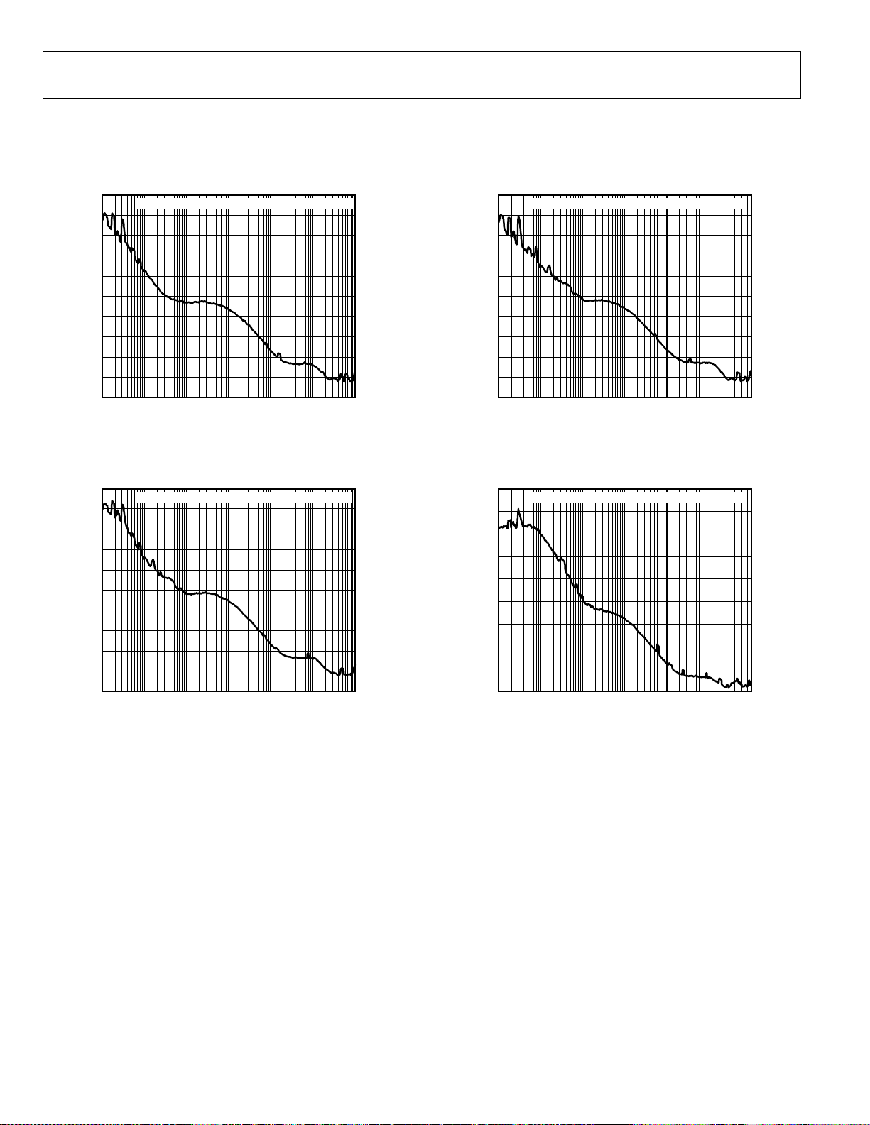
Figure 3. Absolute Phase Noise (Output Driver = HSTL),
f
= 19.44 MHz, f
R
DPLL Loop BW = 50 Hz, f
INTEGRATED RMS JITT ER (12kHz TO 20MHz): 320fs
1k100
FREQUENCY OFFSET (Hz)
OUT
SYS
100k 1M 10M 100M
10k
Figure 4. Absolute Phase Noise (Output Driver = HSTL),
f
= 19.44 MHz, f
R
DPLL Loop BW = 50 Hz, f
= 644.53125 MHz,
OUT
SYS
= output clock frequency; f
OUT
= 622.08 MHz,
= 49.152 MHz Crystal
= 49.152 MHz Crystal
= SYSCLK input frequency; fS = internal system clock frequency;
SYS
= 786.432 MHz, unless otherwise noted.
S
60
–70
–80
–90
–100
–110
–120
–130
PHASE NOISE (dBc/Hz)
–140
–150
–160
09758-003
INTEGRATED RMS JIT TER (12kHz TO 20MHz) : 285fs
1k100 10k 100k 1M 10M 100M
FREQUENCY OFFSET (Hz)
09758-005
Figure 5. Absolute Phase Noise (Output Driver = HSTL),
f
= 19.44 MHz, f
R
DPLL Loop BW = 50 Hz, f
70
–80
–90
–100
–110
–120
–130
PHASE NOI SE (d Bc/Hz)
–140
–150
–160
09758-004
INTEGRATED RMS JITTER (12kHz TO 20MHz): 301fs
1k100
10k
FREQUENCY OFFSET (Hz)
= 693.482991 MHz,
OUT
= 49.152 MHz Crystal
SYS
100k 1M 10M 100M
09758-006
Figure 6. Absolute Phase Noise (Output Driver = HSTL),
= 19.44 MHz, f
f
R
DPLL Loop BW = 1 kHz, f
= 174.703 MHz,
OUT
= 49.152 MHz Crystal
SYS
Rev. A | Page 20 of 104
Data Sheet AD9558
–
–
–
–
–
–
PHASE NOISE (dBc/Hz)
80
–90
–100
–110
–120
–130
–140
–150
–160
INTEGRATED RMS JITT ER (12kHz TO 20MHz): 302fs
1k100 10k 100k 1M 10M 100M
FREQUENCY OFFSET (Hz)
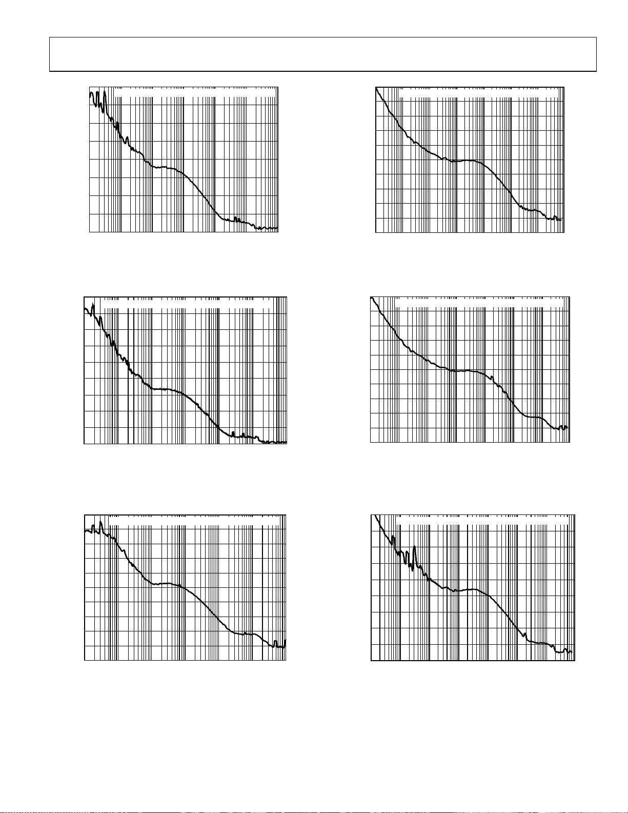
Figure 7. Absolute Phase Noise (Output Driver = 3.3.V CMOS),
PHASE NOISE ( dBc/Hz)
–80
–90
–100
–110
–120
–130
–140
–150
–160
= 19.44 MHz, f
f
R
DPLL Loop BW = 100 Hz, f
70
INTEGRATED RMS JI TTER (12kHz TO 20MHz): 308fs
1k100 10k 100k 1M 10M 100M
FREQUENCY OFFSET (Hz)
= 161.1328125 MHz,
OUT
= 49.152 MHz Crystal
SYS
Figure 8. Absolute Phase Noise (Output Driver = HSTL),
f
= 2 kHz, f
R
DPLL Loop BW = 100 Hz, f
= 125 MHz,
OUT
= 49.152 MHz Crystal
SYS
09758-007
09758-008
PHASE NOISE (dBc/Hz)
60
–70
–80
–90
–100
–110
–120
–130
–140
–150
–160
INTEGRATED RMS JITT ER (12kHz TO 20MHz): 393fs
1k10 100 10k 100k 1M 10M 100M
FREQUENCY OFFSET (Hz)
Figure 10. Absolute Phase Noise (Output Driver = HSTL),
PHASE NOISE (dBc/Hz)
–70
–80
–90
–100
–110
–120
–130
–140
–150
–160
= 19.44 MHz, f
f
R
DPLL Loop BW = 0.1 Hz, f
60
INTEGRATED RMS JITTER (12kHz TO 20MHz): 371s
1k10 100 10k 100k 1M 10M 100M
FREQUENCY O FFSET (Hz)
= 644.53 MHz,
OUT
= 19.2 MHz TCXO
SYS
Figure 11. Absolute Phase Noise (Output Driver = HSTL),
= 19.44 MHz, f
f
R
DPLL Loop BW = 0.1 Hz, f
= 693.482991 MHz,
OUT
= 19.2 MHz TCXO
SYS
09758-010
09758-011
PHASE NOISE (dBc/Hz)
60
–70
–80
–90
–100
–110
–120
–130
–140
–150
–160
INTEG RATED RMS JIT TER (12kHz TO 20MHz): 343fs
1k100 10k 100k 1M 10M 100M
FREQUENCY OF FSET (Hz )
Figure 9. Absolute Phase Noise (Output Driver = HSTL),
= 25 MHz, f
f
R
DPLL Loop BW = 500 Hz, f
= 1 GHz,
OUT
= 49.152 MHz Crystal
SYS
09758-009
PHASE NOI SE (dBc/Hz)
70
–80
–90
–100
–110
–120
–130
–140
–150
–160
INTEG RATED RMS JITT ER (12kHz TO 20MHz): 404fs
1k10 100 10k 100k 1M 10M 100M
FREQUENCY OFFSET (Hz)
Figure 12. Absolute Phase Noise (Output Driver = HSTL),
= 19.44 MHz, f
f
R
DPLL Loop BW = 0.1 Hz, f
= 312.5 MHz,
OUT
= 19.2 MHz TCXO
SYS
09758-012
Rev. A | Page 21 of 104
AD9558 Data Sheet
–
–
–
A
2.0
1.9
1.8
1.7
1.6
1.5
1.4
L PEAK-TO-PEAK AMPLITUDE (V)
1.3
1.2
1.1
DIFFERE NTI
1.0
0
100
200
300
400
500
600
700
800
900
1100
1000
1200
FREQUENC Y (MHz)
1300
09758-116
PHASE NOISE (dBc/Hz)
–80
–90
–100
–110
–120
–130
–140
–150
–160
70
INTEGRATED RMS JITTE R (12kHz TO 20MHz) : 391fs
1k10 100 10k 100k 1M 10M 100M
FREQUENCY OFFSET (Hz)
09758-013
Figure 13. Absolute Phase Noise (Output Driver = 3.3 V CMOS),
PHASE NOI SE (d Bc/Hz)
–80
–90
–100
–110
–120
–130
–140
–150
–160
f
R
DPLL Loop BW = 0.1 Hz, f
70
INTEGRATED RM S JITT ER (12kHz TO 20MHz): 395fs
= 19.44 MHz, f
1k10 100
FREQUENCY O FFSET (Hz)
=161.1328125 MHz,
OUT
= 19.2 MHz TCXO
SYS
100k 1M 10M 100M
10k
Figure 14. Absolute Phase Noise (Output Driver = 1.8 V CMOS),
f
PHASE NOISE (dBc/Hz)
–70
–80
–90
–100
–110
–120
–130
–140
–150
–160
DPLL Loop BW = 0.1 Hz, f
60
INTEGRATED RMS JITTE R (12kHz TO 20MHz) : 388fs
= 2 kHz, f
R
1k10 100 10k 100k 1M 10M 100M
FREQUENCY OFFSET (Hz)
= 70.656 MHz,
OUT
= 19.2 MHz TCXO
SYS
Figure 15. Absolute Phase Noise (Output Driver = HSTL),
= 19.44 MHz, f
f
R
= 644.53 MHz, f
OUT
= 19.2 MHz TCXO
SYS
Holdover Mode
Figure 16. Amplitude vs. Toggle Rate,
HSTL Mode (LVPECL-Compatible Mode)
1.0
0.9
0.8
0.7
0.6
0.5
DIFFERENTIAL PEAK-TO-PEAK AMPLITUDE (V)
0.4
0 100 200 300 400 500 600 700 800
09758-014
LVDS BOOST MODE
LVDS DEFAULT
FREQUE NCY (MHz)
09758-117
Figure 17. Amplitude vs. Toggle Rate, LVDS
3.5
3.0
2.5
2.0
PEAK-TO-PEAK AMPLITUDE (V)
1.5
1.0
0 50 100 150 200 250 300
09758-016
1.8V CMO S
FREQUENC Y (MHz)
3.3V CMO S
09758-118
Figure 18. Amplitude vs. Toggle Rate with 10 pF Load,
3.3 V (Strong Mode) and 1.8 V CMOS
Rev. A | Page 22 of 104
Data Sheet AD9558
A
3.5
3.0
2.5
70
1.8V CMOS MODE
60
50
3.3V CMOS STRONG MODE
3.3V CMOS WEAK MODE
2.0
1.5
1.0
PEAK-TO-PEAK AMPLITUDE (V)
0.5
0
0 1020304050607080
FREQUENCY (MHz)
09758-119
Figure 19. Amplitude vs. Toggle Rate with 10 pF Load,
3.3 V (Weak Mode) CMOS
110
105
100
95
90
85
80
75
70
65
POWER (mW)
60
55
50
45
40
35
30
OUTPUT CHANNEL 1 OR 2:
BOTH HSTL DRIVERS ENABLED
OUTPUT CHANNEL 1 OR 2:
ONE HSTL DRIVER ENABLED
OUTPUT CHANNEL 0 OR 3:
HSTL DRIVER ENABLED
0 250 500 750 1000 1250
FREQUENCY (MHz)
09758-120
Figure 20. Power Consumption vs. Frequency,
HSTL Mode (Single Channel) on 1.8 V Output Driver Power Supply Only
(Pin 12, Pin 17, Pin 22, and Pin29)
65
60
OUTPUT CHANNEL 1 OR 2:
55
BOTH LVDS DRIVERS ENABLED
50
45
40
35
30
25
POWER (mW)
OUTPUT CHANNEL 0 OR 3:
20
LVDS DRIVER ENABLED
15
10
5
0
0 100 200 300 400 500 600 700 800
OUTPUT CHANNEL 1 OR 2:
ONE LVDS DRIVER ENABLED
FREQUENCY (MHz)
9758-121
Figure 21. LVDS Power Consumption vs. Frequency on 1.8 V Output Driver
Power Supply Only (Pin 12, Pin 17, Pin 22, and Pin 29)
40
30
POWER (mW)
20
10
0
0 50 100 150 200
FREQUENCY (MHz)
09758-122
Figure 22. Power Consumption vs. Frequency, One CMOS Driver on Output
Driver Power Supply Only (Pin 12, Pin 17, Pin 22, and Pin 29) for 1.8 V CMOS Mode,
or on Pin 25 and Pin 26 for 3.3 V CMOS Mode
1.0
0.8
0.6
0.4
0.2
0
LAMPLITUDE (V)
–0.2
–0.4
DIFFERENTI
–0.6
–0.8
–1.0
–101234
TIME (ns)
5
09758-123
Figure 23. Output Waveform, HSTL (400 MHz)
0.4
0.3
0.2
0.1
0
–0.1
–0.2
DIFFERE NTIAL AMP LITUDE (V)
–0.3
–0.4
–101234
TIME (ns)
09758-124
Figure 24. Output Waveform, LVDS (400 MHz)
Rev. A | Page 23 of 104
AD9558 Data Sheet
O
O
3.4
3.0
2.6
2.2
1.8
1.4
AMPLIT UDE (V)
1.0
0.6
0.2
–0.2
–10123456789101112131415
2pF LOAD
10pF LOAD
TIME (ns)
Figure 25. Output Waveform,
3.3 V CMOS (100 MHz, Strong Mode)
1.9
1.7
1.5
1.3
1.1
0.9
0.7
AMPLIT UDE (V)
0.5
0.3
0.1
–0.1
–10123456789101112131415
2pF LOAD
10pF LOAD
TIME (ns)
Figure 26. Output Waveform, 1.8 V CMOS (100 MHz)
09758-126
09758-127
3
0
–3
–6
–9
–12
–15
P GAIN (dB)
–18
LO
LOOP BW = 100Hz;
–21
HIGH PHASE MARGIN;
PEAKING: 0.06dB; –3dB: 69Hz
LOOP BW = 2kHz;
–24
HIGH PHASE MARGIN;
PEAKING: 0.097dB; –3dB: 1.23kHz
–27
LOOP BW = 5kHz;
HIGH PHASE MARGIN;
PEAKING: 0.14dB; –3dB: 4.27kHz
–30
10 100 1k 10k 100k
FREQUENCY OFF SET (Hz)
09758-129
Figure 28. Closed-Loop Transfer Function for 100 Hz, 2 kHz, and 5 kHz Loop
Bandwidth Settings; High Phase Margin Loop Filter Setting
(This is compliant with Telcordia GR-253 jitter transfer test for loop
bandwidths < 2 kHz.)
3
0
–3
–6
–9
–12
–15
P GAIN (dB)
–18
LO
–21
LOOP BW = 100Hz;
NORMAL PHASE MARGIN;
–24
PEAKING: 0.09dB; –3dB: 117Hz
LOOP BW = 2k Hz;
NORMAL PHASE MARGIN;
–27
PEAKING: 1.6dB; –3dB: 2.69kHz
–30
10 100 1k
FREQUENCY OFF SET (Hz)
10k 100k
09758-230
Figure 29. Closed-Loop Transfer Function for 100 Hz and 2 kHz Loop
Bandwidth Settings; Normal Phase Margin Loop Filter Setting
3.2
2pF LOAD
10pF LOAD
2.8
2.4
2.0
1.6
AMPLITUDE (V)
1.2
0.8
0.4
0
–5 5 152535455565758595
TIME (ns)
09758-128
Figure 27. Output Waveform, 3.3 V CMOS (20 MHz, Weak Mode)
Rev. A | Page 24 of 104
Data Sheet AD9558
V
V
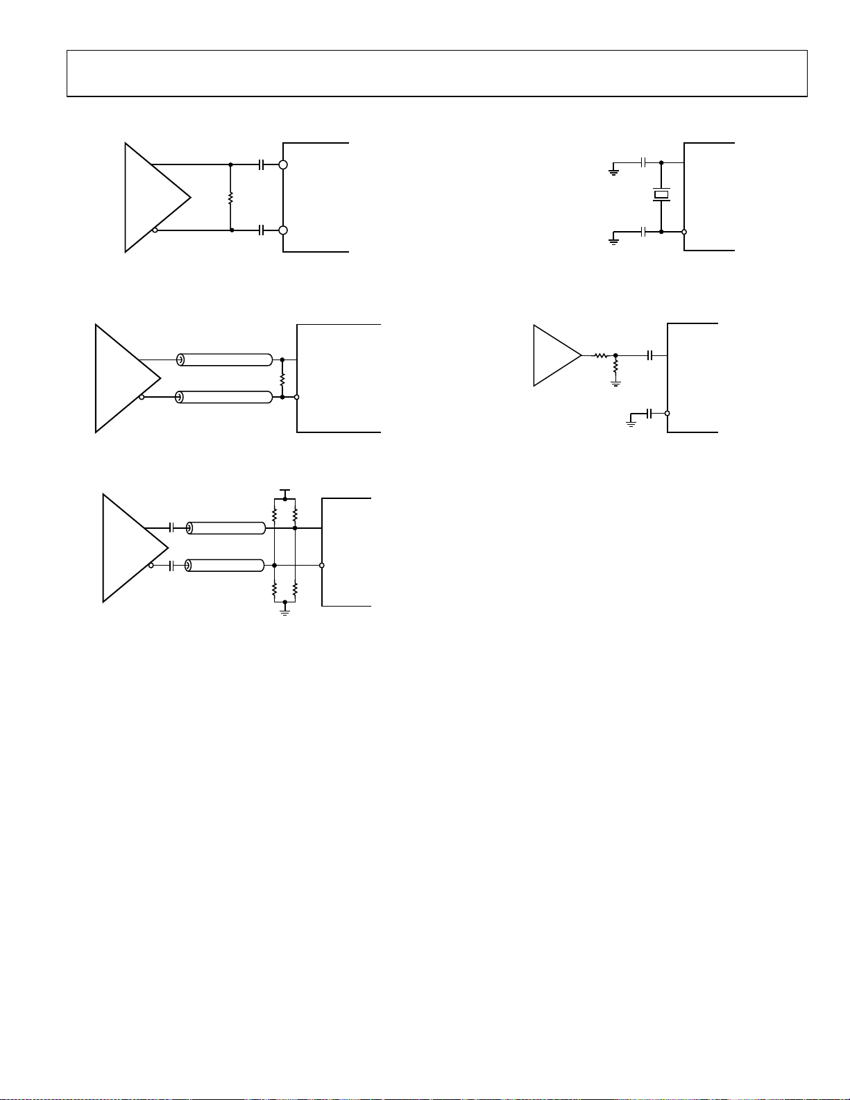
INPUT/OUTPUT TERMINATION RECOMMENDATIONS
0.1µF
DOWNSTREAM
DEVICE
AD9557/
AD9558
HSTL OR
LVDS
100Ω
0.1µF
WITH HIGH
IMPEDANCE
INPUT AND
INTERNAL
DC BIAS
09758-130
Figure 30. AC-Coupled LVDS or HSTL Output Driver
(100 Ω resistor can go on either side of decoupling capacitors and should be
as close as possible to the destination receiver.)
10MHz TO 50MHz F UNDAMENTAL
AT CUT CRYST AL WIT H
10pF LO AD CAPACITANCE
Figure 33. System Clock Input (XOA, XOB) in Crystal Mode
(The recommended C
= 10 pF is shown. The values of the 10 pF shunt
LOAD
capacitors shown here should equal the C
10pF
10pF
XOA
AD9557/
AD9558
XOB
of the crystal.)
LOAD
09758-133
Z0 = 50Ω
AD9557/
AD9558
HSTL OR
LVDS
SINGLE-ENDED
(NOT COUPL ED)
= 50Ω
Z
0
100Ω
LVDS OR 1.8V HS TL
HIGH IMPEDANCE
DIFFERE NTIAL
RECEIVER
09758-131
Figure 31. DC-Coupled LVDS or HSTL Output Driver
= 3.3
S
82Ω82Ω
3.3V
LVPECL
127Ω127Ω
09758-132
AD9557/
AD9558
1.8V
HSTL
0.1µF
0.1µF
Z0 = 50Ω
SINGLE -ENDED
(NOT COUPLED)
= 50Ω
Z
0
Figure 32. Interfacing the HSTL Driver to a 3.3 V LVPECL Input
(This method incorporates impedance matching and dc biasing for bipolar
LVPECL receivers. If the receiver is self-biased, the termination scheme shown
in Figure 30 is recommended.)
150Ω
0.1µF
0.1µF
XOA
AD9557/
AD9558
XOB
09758-134
3.3V
CMOS
TCXO
300Ω
Figure 34. System Clock Input (XOA, XOB) When Using a TCXO/OCXO with
3.3 V CMOS Output
Rev. A | Page 25 of 104

AD9558 Data Sheet
GETTING STARTED
CHIP POWER MONITOR AND STARTUP
The AD9558 monitors the voltage on the power supplies at
power-up. When DVDD3 is greater than 2.35 V ± 0.1 V and
DVDD and AVDD are greater than 1.4 V ± 0.05 V, the device
generates a 20 ms reset pulse. The power-up reset pulse is internal
and independent of the
sequence eliminates the need for the user to provide external power
supply sequencing. Within 45 ns after the leading edge of the
internal reset pulse, the M7 to M0 multifunction pins behave
as high impedance digital inputs and continue to do so until
programmed otherwise. The delay on the M7 to M0 pin function
change is 45 ns for pin reset or soft reset.
During a device reset (either via the power-up reset pulse or the
RESET
pin), the multifunction pins (M7 to M0) behave as high
impedance inputs, but upon removal of the reset condition,
level-sensitive latches capture the logic pattern present on the
multifunction pins.
RESET
pin. This internal power-up reset
MULTIFUNCTION PINS AT RESET/POWER-UP
The AD9558 requires the user to supply the desired logic state
to the PINCONTROL pin, as well as to the M7 to M0 pins. If
PINCONTROL is high, the part is in hard pin programming
mode. See the Pin Program Function Description section for
details on hard pin programming.
At startup, there are three choices for the M7 to M0 pins: pullup, pull-down, and floating. If the PINCONTROL pin is low,
the M7 to M0 pins determine the following configurations:
• Following a reset, the M1 and M0 pins determine whether
the serial port interface behaves according to the SPI or I
protocol. Specifically, M0 = M1 = low selects the SPI
interface, and any other value selects the I
level logic of M1 and M0 allows the user to select eight
possible I
• The M3 and M2 pins select which of the eight possible
EEPROM profiles are loaded, or if the EEPROM loading is
bypassed. Leaving M3 and M2 floating at startup bypasses
the EEPROM loading, and the factory defaults are used
instead (see Tab l e 2 2 ).
2
C addresses (see Tabl e 24 ).
2
C port. The 3-
2
C
DEVICE REGISTER PROGRAMMING WHEN USING A REGISTER SETUP FILE
The evaluation software contains a programming wizard and
a convenient graphical user interface that assists the user in
determining the optimal configuration for the DPLL, APLL,
and SYSCLK based on the desired input and output frequencies.
It generates a register setup file with a .STP extension that is
easily readable using a text editor.
After using the evaluation software to create the setup file, use
the following sequence to program the AD9557 once:
1. Register 0x0A01 = 0x20 (set user free run mode).
2. Register 0x0A02 = 0x02 (hold outputs in static SYNC).
(Skip this step if using SYNC on DPLL phase lock or SYNC
on DPLL frequency lock. See Register 0x0500[1:0].)
3. Register 0x0405 = 0x20 (clear APLL VCO calibration).
4. Write the register values in the STP file from Address 0x0000
to Address 0x032E.
5. Register 0x0005 = 0x01 (update all registers).
6. Write the rest of the registers in the STP file, starting at
Address 0x0400.
7. Register 0x0405 = 0x21 (calibrate APLLon next I/O update).
8. Register 0x0403 = 0x07 (configure APLL).
9. Register 0x0400 = 0x81 (configure APLL).
10. Register 0x0005 = 0x01 (update all registers).
11. Register 0x0A01[5] = 0b (clear user free run mode).
12. Register 0x0005 = 0x01 (update all registers).
REGISTER PROGRAMMING OVERVIEW
This section provides an overview of the register blocks in the
AD9558, describing what they do and why they are important.
Registers Differing from Defaults for Optimal Performance
Ensure that the following registers are programmed to the listed
values for optimal performance:
• Register 0x0405[7:4] = 0x2
• Register 0x0403 = 0x07
• Register 0x0400 = 0x81
If the silicon revision (Register 0x000A) equals 0x21 or higher,
the values listed here are already the default values.
Rev. A | Page 26 of 104

Data Sheet AD9558
Program the System Clock and Free Run Tuning Word
The system clock multiplier (SYSCLK) parameters are at
Register 0x0100 to Register 0x0108, and the free run tuning
word is at Register 0x0300 to Register 0x0303. Use the following
steps for optimal performance:
1. Set the system clock PLL input type and divider values.
2. Set the system clock period.
It is essential to program the system clock period because
many of the AD9558 subsystems rely on this value.
3. Set the system clock stability timer.
It is highly recommended that the system clock stability
timer be programmed. This is especially important when
using the system clock multiplier and also applies when
using an external system clock source, especially if the
external source is not expected to be completely stable
when power is applied to the AD9558. The system clock
stability timer specifies the amount of time that the system
clock PLL must be locked before the part declares that the
system clock is stable. The default value is 50 ms.
4. Program the free run tuning word.
The free run frequency of the digital PLL (DPLL) determines
the frequency appearing at the APLL input when free run
mode is selected. The free run tuning word is at Register
0x0300 to Register 0x0303. The correct free run frequency
is required for the APLL to calibrate and lock correctly.
5. Set user free run mode (Register 0x0A01[5] = 1b).
Initialize and Calibrate the Output PLL (APLL)
The registers controlling the APLL are at Register 0x0400
to Register 0x0408. This low noise, integer-N PLL multiplies
the DPLL output (which is usually 175 MHz to 200 MHz) to a
frequency in the 3.35 GHz to 4.05 GHz range. After the system
clock is configured and the free run tuning word is set in
Register 0x0300 to Register 0x0303, the user can set the manual
APLL VCO calibration bit (Register 0x0405[0]) and issue an I/O
update (Register 0x0005[0]). This process performs the APLL
VCO calibration. VCO calibration ensures that, at the time of
calibration, the dc control voltage of the APLL VCO is centered in
the middle of its operating range. It is important to remember the
following points when calibrating the APLL VCO:
• The system clock must be stable.
• The APLL VCO must have the correct frequency from the
30-bit DCO (digitally controlled oscillator) during
calibration.
• The APLL VCO must be recalibrated any time the APLL
frequency changes.
• APLL VCO calibration occurs on the low-to-high transition
of the manual APLL VCO calibration bit, and this bit is not
autoclearing. Therefore, this bit must be cleared (and an I/O
update issued) before another APLL calibration is started.
• The best way to monitor successful APLL calibration is to
monitor Bit 2 in Register 0x0D01 (APLL lock).
Program the Clock Distribution Outputs
The APLL output goes to the clock distribution block. The
clock distribution parameters reside in Register 0x0500 to
Register 0x0509. They include the following:
• Output power-down control
• Output enable (disabled by default)
• Output synchronization
• Output mode control
• Output divider functionality
See the Clock Distribution section for more information.
Generate the Output Clock
If Register 0x0500[1:0] is programmed for automatic clock
distribution synchronization via the DPLL phase or frequency
lock, the synthesized output signal appears at the clock distribution
outputs. Otherwise, set and then clear the soft sync clock
distribution bit (Register 0x0A02, Bit 1), or use a multifunction
pin input (if programmed for use) to generate a clock
distribution sync pulse, which causes the synthesized output
signal to appear at the clock distribution outputs.
Program the Multifunction Pins (Optional)
This step is required only if the user intends to use any of the
multifunction pins for status or control. The multifunction pin
parameters are at Register 0x0200 to Register 0x0208.
Program the IRQ Functionality (Optional)
This step is required only if the user intends to use the IRQ feature.
The IRQ monitor registers are at Register 0x0D02 to Register
0x0D09. If the desired bits in the IRQ mask registers at Register
0x020A to Register 0x020F are set high, the appropriate IRQ
monitor bit at Register 0x0D02 to Register 0x0D07 is set high
when the indicated event occurs.
Individual IRQ events are cleared by using the IRQ clearing
registers at Register 0x0A04 to Register 0x0A09, or by setting
the clear all IRQs bit (Register 0x0A03[1]) to 1b.
The default values of the IRQ mask registers are such that
interrupts are not generated. The IRQ pin mode default is opendrain NMOS.
Program the Watchdog Timer (Optional)
This step is required only if the user intends to use the watchdog
timer. The watchdog timer control is in Register 0x0210 and
Register 0x0211 and is disabled by default.
The watchdog timer is useful for generating an IRQ after a fixed
amount of time. The timer is reset by setting the clear watchdog
timer bit (Register 0x0A03[0]) to 1b.
Rev. A | Page 27 of 104

AD9558 Data Sheet
Program the Digital Phase-Locked Loop (DPLL)
The DPLL parameters reside in Register 0x0300 to
Register 0x032E. They include the following:
• Free run frequency
• DPLL pull-in range limits
• DPLL closed-loop phase offset
• Phase slew control (for hitless reference switching)
• Tuning word history control (for holdover operation)
Program the Reference Inputs
The reference input parameters reside in Register 0x0600 to
Register 0x0602. See the Reference Clock Input section for
details on programming these functions. They include the
following:
• Reference power-down
• Reference logic family
• Reference priority
Program the Reference Profiles
The reference profile parameters reside in Register 0x0700 to
Register 0x07E6. The AD9558 evaluation software contains a
wizard that calculates these values based on the user’s input
frequency. See the Reference Profiles section for details on
programming these functions. They include the following:
• Reference period
• Reference period tolerance
• Reference validation timer
• Selection of high phase margin loop filter coefficients
• DPLL loop bandwidth
• Reference prescaler (R divider)
• Feedback dividers (N1, N2, N3, FRAC1, and MOD1)
• Phase and frequency lock detector controls
Generate the Reference Acquisition
After the registers are programmed, the user can clear the user
freerun bit (Register 0x0A01[5]) and issue an I/O update, using
Register 0x0005[0] to invoke all of the register settings that are
programmed up to this point.
After the registers are programmed, the DPLL locks to the first
available valid reference that has the highest priority.
Rev. A | Page 28 of 104
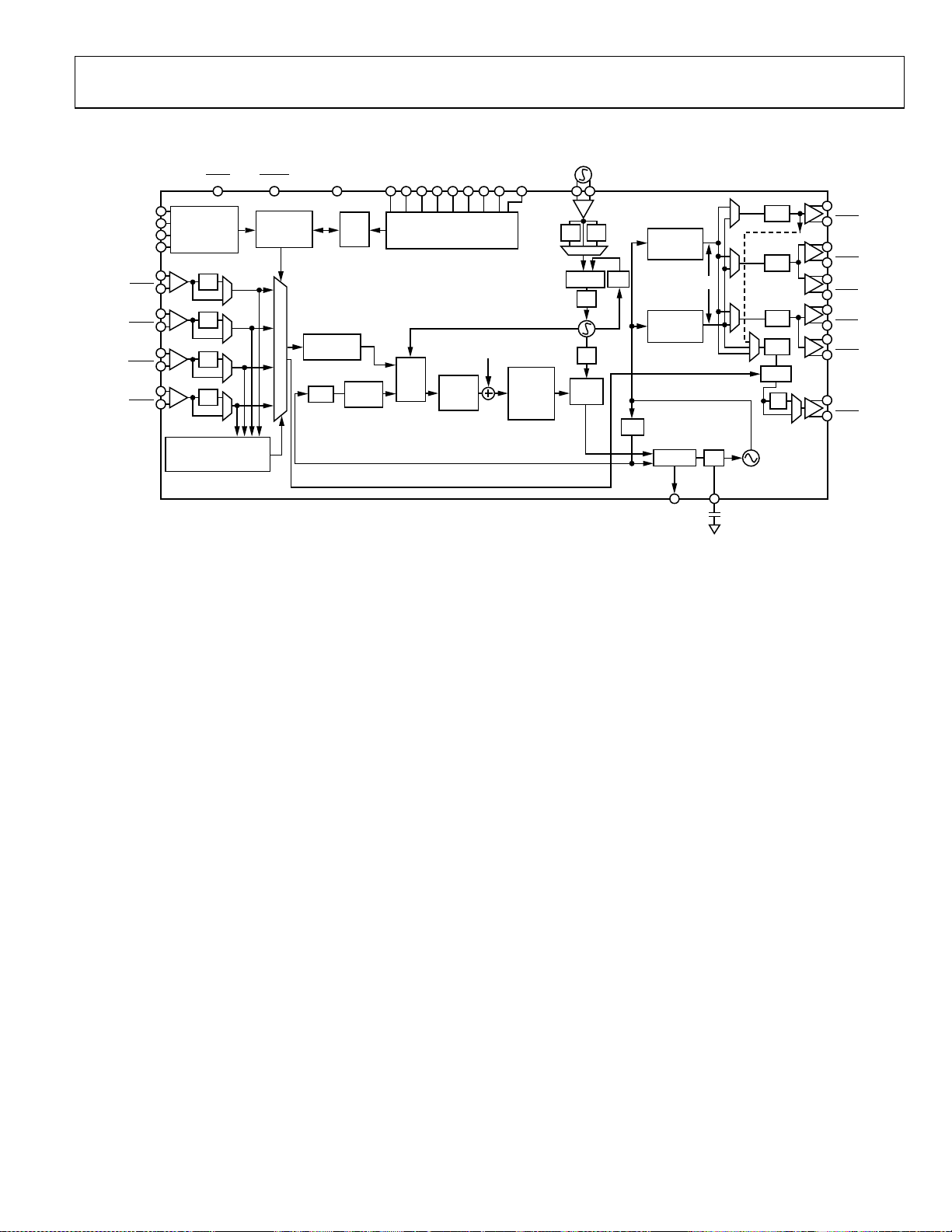
Data Sheet AD9558
X
THEORY OF OPERATION
SYNC RESET PINCONTROL M0 M1 M2 M3 IRQ
SPI/I
REFA
REFA
REFC
REFC
2kHz TO 1.25GHz
2
REFB
REFB
REFD
REFD
C
SERIAL PORT
REF MONITORING
SPI/I2C
EEPROM
÷2
÷2
÷2
÷2
AUTOMATIC
SWITCHING
REGISTER
SPACE
AD9558
1
OUT0, OUT1, OUT2, OUT3, O UT4: 360kHz TO 1.25GHz; O UT5: 352Hz TO 1.25GHz
ROM
AND
FSM
R DIVIDER
(20-BIT)
17-BIT
INTEGER
FRAC1/
÷N1
24b/24b
RESOLUTION
2kHz TO 8kHz FRAME S YNC SIGNAL
MULTIFUNCTION I/O PINS
(CONTROL AND STATUS
DPFD
MOD1
OVERVIEW
The AD9558 provides clocking outputs that are directly related
in phase and frequency to the selected (active) reference, but
with jitter characteristics that are governed by the system clock,
the DCO, and the output PLL (APLL). The AD9558 supports
up to four reference inputs and input frequencies ranging from
2 kHz to 1250 MHz. The core of this product is a digital phaselocked loop (DPLL). The DPLL has a programmable digital loop
filter that greatly reduces jitter that is transferred from the active
reference to the output. The AD9558 supports both manual and
automatic holdover. While in holdover, the AD9558 continues to
provide an output as long as the system clock is present. The
holdover output frequency is a time average of the output
frequency history just prior to the transition to the holdover
condition. The device offers manual and automatic reference
switchover capability if the active reference is degraded or fails
completely. The AD9558 also has adaptive clocking capability
that allows the DPLL divider ratios to be changed while the DPLL
is locked.
The AD9558 has a system clock multiplier, a digital PLL (DPLL),
and an analog PLL (APLL). The input signal goes first to the DPLL,
which performs the jitter cleaning and most of the frequency
translation. The DPLL features a 30-bit digitally controlled
oscillator (DCO) output that generates a signal in the 175 MHz
to 200 MHz range. The DPLL output goes to an analog integer-N
PLL (APLL), which multiplies the signal up to the 3.35 GHz to
4.05 GHz range. That signal is then sent to the clock distribution
M4 M5 M6 M7
READBACK)
DIGITAL
LOOP
FILTER
DIGITAL PLL (DPL L)
Figure 35. Detailed Block Diagram
FREE RUN
TW
SYSTEM
CLOCK
MULTIPLIER
TUNING
WORD
CLAMP
AND
HISTORY
O OR XTAL
÷2
PFD/CP
30-BIT
NCO
XO FREQUENCIES
10MHz TO 180MHz
XTAL: 10MHz TO 50MHz
×2
÷N3
LF
×2
FRAME SYNC PULSE
÷N2
RF
DIVIDER 1
÷3 TO ÷11
MAX 1.25GHz
RF
DIVIDER 2
÷3 TO ÷11
OUTPUT PLL (APLL)
PFD/CP
APLL
STATUS
LF
LF_VCO2
÷M0 TO ÷M3b ARE
10-BIT INTEGER
DIVIDERS
÷M0
FRAME SYNC
MODE ON LY
÷M1
÷M2
÷M3
÷M3b
×2
3.35GHz
TO
4.05GHz
OUT0
OUT0
OUT1
OUT1
OUT2
OUT2
OUT3
OUT3
OUT4
OUT4
OUT5
OUT5
1
section, which has two divide-by-3 to divide-by-11 RF dividers
that are cascaded with 10-bit integer (divide-by-1 to divide-by-
1024) channel dividers.
The XOA and XOB pins provide the input for the system clock.
These pins accept a reference clock in the 10 MHz to 600 MHz
range, or a 10 MHz to 50 MHz crystal connected directly across
the XOA and XOB pins. The system clock provides the clocks to
the frequency monitors, the DPLL, and internal switching logic.
The AD9558 has six output drivers, arranged into four channels.
Each channel has a dedicated 10-bit programmable post divider.
Channel 0 and Channel 3 have one driver each, and Channel 1
and Channel 2 have two drivers each. Each driver is programmable
either as a single differential or dual single-ended CMOS output.
The clock distribution section operates at up to 1250 MHz.
In differential mode, the output drivers run on a 1.8 V power
supply to offer very high performance with minimal power
consumption. There are two differential modes: LVDS and 1.8 V
HSTL. In 1.8 V HSTL mode, the voltage swing is compatible
with LVPECL. If LVPECL signal levels are required, the designer
can ac-couple the AD9558 output and use Thevenin-equivalent
termination at the destination to drive the LVPECL inputs.
In single-ended mode, each differential output driver can
operate as two single-ended CMOS outputs. OUT0 and OUT5
support either 1.8 V or 3.3 V CMOS operation. OUT1 through
OUT4 support only 1.8 V operation.
1
1
1
1
1
1
1
1
1
1
1
9758-135
Rev. A | Page 29 of 104

AD9558 Data Sheet
REFERENCE CLOCK INPUTS
Four pairs of pins provide access to the reference clock receivers.
To accommodate input signals with slow rising and falling edges,
both the differential and single-ended input receivers employ
hysteresis. Hysteresis also ensures that a disconnected or
floating input does not cause the receiver to oscillate.
When configured for differential operation, the input receivers
accommodate either ac- or dc-coupled input signals. The input
receivers are capable of accepting dc-coupled LVDS and 2.5 V
and 3.3 V LVPECL signals. The receiver is internally dc biased
to handle ac-coupled operation, but there is no internal 50 Ω or
100 Ω termination.
When configured for single-ended operation, the input
receivers exhibit a pull-down load of 45 kΩ (typical). Three
user-programmable threshold voltage ranges are available for
each single-ended receiver.
REFERENCE MONITORS
The accuracy of the input reference monitors depends on a
known and accurate system clock period. Therefore, the
functioning of the reference monitors is not operable until the
system clock is stable.
Reference Period Monitor
Each reference input has a dedicated monitor that repeatedly
measures the reference period. The AD9558 uses the reference
period measurements to determine the validity of the reference
based on a set of user-provided parameters in the profile
register area of the register map.
The monitor works by comparing the measured period of a
particular reference input with the parameters stored in the
profile register assigned to that same reference input. The
parameters include the reference period, an inner tolerance,
and an outer tolerance. A 40-bit number defines the reference
period in units of femtoseconds (fs). The 40-bit range allows for
a reference period entry of up to 1.1 ms. A 20-bit number defines
the inner and outer tolerances. The value stored in the register
is the reciprocal of the tolerance specification. For example, a
tolerance specification of 50 ppm yields a register value of
1/(50 ppm) = 1/0.000050 = 20,000 (0x04E20).
The use of two tolerance values provides hysteresis for the
monitor decision logic. The inner tolerance applies to a
previously faulted reference and specifies the largest period
tolerance that a previously faulted reference can exhibit before it
qualifies as nonfaulted. The outer tolerance applies to an already
nonfaulted reference. It specifies the largest period tolerance
that a nonfaulted reference can exhibit before being faulted.
To produce decision hysteresis, the inner tolerance must be less
than the outer tolerance. That is, a faulted reference must meet
tighter requirements to become nonfaulted than a nonfaulted
reference must meet to become faulted.
Reference Validation Timer
Each reference input has a dedicated validation timer. The
validation timer establishes the amount of time that a previously
faulted reference must remain unfaulted before the AD9558
declares it valid. The timeout period of the validation timer is
programmable via a 16-bit register. The 16-bit number stored
in the validation register represents units of milliseconds (ms),
which yields a maximum timeout period of 65,535 ms.
It is possible to disable the validation timer by programming the
validation timer to 0b. With the validation timer disabled, the
user must validate a reference manually via the manual reference
validation override controls register (Address 0x0A0B).
Reference Validation Override Control
The user also has the ability to override the reference validation
logic and can either force an invalid reference to be treated as
valid, or force a valid reference to be treated as an invalid
reference. These controls are in Register 0x0A0B to Register
0x0A0D.
REFERENCE PROFILES
The AD9558 has an independent profile for each reference input.
A profile consists of a set of device parameters such as the R divider
and N divider, among others The profiles allow the user to
prescribe the specific device functionality that should take effect
when one of the input references becomes the active reference.
The AD9558 evaluation software includes a frequency planning
wizard that can configure the profile parameters, given the
input and output frequencies.
The user should not change a profile that is currently in use
because unpredictable behavior may result. The user can either
select free run or holdover mode or invalidate the reference
input prior to changing it.
REFERENCE SWITCHOVER
An attractive feature of the AD9558 is its versatile reference
switchover capability. The flexibility of the reference switchover
functionality resides in a sophisticated prioritization algorithm
that is coupled with register-based controls. This scheme
provides the user with maximum control over the state machine
that handles reference switchover.
The main reference switchover control resides in the loop
mode register (Address 0x0A01). The REF switchover mode
bits (Register 0x0A01, Bits[4:2]) allow the user to select one of
the five operating modes of the reference switchover state machine,
as follows:
• Automatic revertive mode
• Automatic non-revertive mode
• Manual with automatic fallback mode
• Manual with holdover mode
• Full manual mode (without auto-holdover)
Rev. A | Page 30 of 104

Data Sheet AD9558
In the automatic modes, a fully automatic priority-based algorithm
selects which reference is the active reference. When programmed
for an automatic mode, the device chooses the highest priority
valid reference. When both references have the same priority,
REFA gets preference over REFB. However, the reference position
is used only as a tie-breaker and does not initiate a reference switch.
The following list gives an overview of the five operating modes:
• Automatic revertive mode. The device selects the highest
priority valid reference and switches to a higher priority
reference if it becomes available, even if the reference in use
is still valid. In this mode, the user reference is ignored.
• Automatic non-revertive mode. The device stays with the
currently selected reference as long as it is valid, even if
a higher priority reference becomes available. The user
reference is ignored in this mode.
• Manual with automatic fallback mode. The device uses the
user reference for as long as it is valid. If it becomes invalid,
the reference input with the highest priority is chosen in
accordance with the priority-based algorithm.
• Manual with holdover mode. The user reference is the
active reference until it becomes invalid. At that point,
the device automatically goes into holdover.
• Manual mode without holdover. The user reference is the
active reference, regardless of whether or not it is valid.
The user also has the option to force the device directly into
holdover or free run operation via the user holdover and user
freerun bits. In free run mode, the free run frequency tuning
word register defines the free run output frequency. In holdover
mode, the output frequency depends on the holdover control
settings (see the Holdover section).
Phase Build-Out Reference Switching
The AD9558 supports phase build-out reference switching,
which is the term given to a reference switchover that
completely masks any phase difference between the previous
reference and the new reference. That is, there is virtually no
phase change detectable at the output when a phase build-out
switchover occurs.
DIGITAL PLL (DPLL) CORE
DPLL Overview
SYSTEM
CLOCK
FROM
REF
INPUT
MUX
÷N1
17-BIT
INTEGER
R DIVIDER
(20-BIT)
FRAC1/
MOD1
24-BIT/24-BIT
RESOLUTION
FREE RUN
TW
DPFD
DIGIT AL
LOOP
FILTER
Figure 36. Digital PLL Core
+
TUNING
WORD
CLAMP
AND
HISTORY
×2
30-BIT NCO
TO APLL
FROM APLL
09758-136
A diagram of the DPLL core of the AD9558 appears in Figure 36.
The phase/frequency detector, feedback path, lock detectors,
phase offset, and phase slew rate limiting that comprise this
second generation DPLL are all digital implementations.
The start of the DPLL signal chain is the reference signal, f
,
R
which is the frequency of the reference input. A reference
prescaler reduces the frequency of this signal by an integer factor,
R + 1, where R is the 20-bit value stored in the appropriate
profile register and 0 ≤ R ≤ 1,048,575. Therefore, the frequency
at the output of the R-divider (or the input to the time-to-digital
converter (TDC)) is
f
f
TDC
R
1+=R
A TDC samples the output of the R-divider. The TDC/PFD
produces a time series of digital words and delivers them to the
digital loop filter. The digital loop filter offers the following
advantages:
• Determination of the filter response by numeric
coefficients rather than by discrete component values
• The absence of analog components (R/L/C), which
eliminates tolerance variations due to aging
• The absence of thermal noise associated with analog
components
• The absence of control node leakage current associated
with analog components (a source of reference feedthrough spurs in the output spectrum of a traditional
analog PLL)
The digital loop filter produces a time series of digital words at
its output and delivers them to the frequency tuning input of a
sigma-delta (Σ-) modulator (SDM). The digital words from
the loop filter steer the DCO frequency toward frequency and
phase lock with the input signal (f
TDC
).
The DPLL includes a feedback divider that causes the digital
loop to operate at an integer-plus-fractional multiple. The
output of the DPLL is
FRAC1
MOD1
⎤
⎥
⎦
⎡
_
TDCDPLLOUT
⎢
⎣
)1(
++×=
N1ff
where N1 is the 17-bit value stored in the appropriate profile
registers (Register 0x0715 to Register 0x0717 for REFA). FRAC1
and MOD1 are the 24-bit numerators and denominators of the
fractional feedback divider block. The fractional portion of the
feedback divider can be bypassed by setting FRAC1 to 0, but
MOD1 should never be 0.
The DPLL output frequency is usually 175 MHz to 200 MHz for
optimal performance.
Rev. A | Page 31 of 104

AD9558 Data Sheet
TDC/PFD
The phase-frequency detector (PFD) is an all-digital block. It
compares the digital output from the TDC (which relates to the
active reference edge) with the digital word from the feedback
block. It uses a digital code pump and digital integrator (rather
than a conventional charge pump and capacitor) to generate the
error signal that steers the DCO frequency toward phase lock.
Programmable Digital Loop Filter
The AD9558 loop filter is a third order digital IIR filter that is
analogous to the third order analog loop shown in Figure 37.
R
3
R
C
1
Figure 37. Third Order Analog Loop Filter
C
2
C
2
3
09758-015
The AD9558 loop filter block features a simplified architecture
in which the user enters the desired loop characteristics directly
into the profile registers. This architecture makes the calculation
of individual coefficients unnecessary in most cases, while still
offering complete flexibility.
The AD9558 has two preset digital loop filters: high (88.5°) phase
margin and normal (70°) phase margin. The loop filter coefficients
are stored in Register 0x0317 to Register 0x0322 for high phase
margin and Register 0x0323 to Register 0x032E for normal phase
margin. The high phase margin loop filter is intended for
applications in which the closed-loop transfer function must
not have greater than 0.1 dB of peaking.
Bit 0 of the following registers selects which filter is used for
each profile: Register 0x070E for Profile A, Register 0x074E for
Profile B, Register 0x078E for Profile C, and Register 0x07CE
for Profile D.
The loop bandwidth for each profile is set in the following
registers: Register 0x070F to Register 0x0711 for Profile A,
Register 0x074F to Register 0x0751 for Profile B, Register 0x078F
to Register 0x0791 for Profile C, and Register 0x07CF to
Register 0x07D1 for Profile D.
The two preset conditions should cover all of the intended
applications for the AD9558. For special cases where these
conditions must be modified, the tools for calculating these
coefficients are available by contacting Analog Devices directly.
DPLL Digitally Controlled Oscillator Free Run Frequency
The AD9558 uses a Σ- modulator (SDM) as a digitally controlled
oscillator (DCO). The DCO free run frequency can be calculated
from the following equation:
2
×=
_
ff
SYSfreerundco
8
+
FTW0
30
2
where FTW0 is the value in Register 0x0300 to Register 0x0303,
and f
is the system clock frequency. See the System Clock
SYS
section for information on calculating the system clock frequency.
Adaptive Clocking
The AD9558 can support adaptive clocking applications such as
asynchronous mapping and demapping. In these applications,
the output frequency can be dynamically adjusted by up to
±100 ppm from the nominal output frequency without manually
breaking the DPLL loop and reprogramming the part. This
function is supported for REFA only, not REFB.
The following registers are used in this function:
• Register 0x0717 (DPLL N1 divider)
• Register 0x0718 to Register 0x071A (DPLL FRAC1 divider)
• Register 0x071B to Register 0x071D (DPLL MOD1
divider)
Writing to these registers requires an I/O update by writing
0x01 to Register 0x0005 before the new values take effect.
To make small adjustments to the output frequency, the user
can vary the FRAC1 and issue an I/O update. The advantage to
using only FRAC1 to adjust the output frequency is that the
DPLL does not briefly enter holdover. Therefore, the FRAC1 bit
can be updated as fast as the phase detector frequency of
the DPLL.
Writing to the N1 and MOD1 dividers allows for larger changes
to the output frequency. When the AD9558 detects that the N1
or MOD1 values have changed, it automatically enters and exits
holdover for a brief instant without any disturbance in the
output frequency. This limits how quickly the output frequency
can be adapted.
It is important to realize that the amount of frequency adjustment
is limited to ±100 ppm before the output PLL (APLL) needs a
recalibration. Variations that are larger than ±100 ppm are
possible, but the ability of the AD9558 to maintain lock over
temperature extremes may be compromised.
It is also important to remember that the rate of change in
output frequency depends on the DPLL loop bandwidth.
Rev. A | Page 32 of 104

Data Sheet AD9558
DPLL Phase Lock Detector
The DPLL contains an all-digital phase lock detector. The user
controls the threshold sensitivity and hysteresis of the phase
detector via the profile registers.
The phase lock detector behaves in a manner analogous to
water in a tub (see Figure 38). The total capacity of the tub is
4096 units with −2048 denoting empty, 0 denoting the 50%
point, and +2048 denoting full. The tub also has a safeguard to
prevent overflow. Furthermore, the tub has a low water mark at
−1024 and a high water mark at +1024. To change the water
level, the user adds water with a fill bucket or removes water
with a drain bucket. The user specifies the size of the fill and
drain buckets via the 8-bit fill rate and drain rate values in the
profile registers.
2048
1024
0
–1024
–2048
PREVIOUS
STATE
LOCKED UNLOCKED
FILL
DRAIN
RATE
RATE
Figure 38. Lock Detector Diagram
LOCK LEVEL
UNLOCK LEVEL
The water level in the tub is what the lock detector uses to
determine the lock and unlock conditions. When the water level
is below the low water mark (−1024), the detector indicates an
unlock condition. Conversely, when the water level is above the
high water mark (+1024), the detector indicates a lock condition.
When the water level is between the marks, the detector simply
holds its last condition. This concept appears graphically in
Figure 38, with an overlay of an example of the instantaneous
water level (vertical) vs. time (horizontal) and the resulting
lock/unlock states.
During any given PFD cycle, the detector either adds water with
the fill bucket or removes water with the drain bucket (one or
the other but not both). The decision of whether to add or
remove water depends on the threshold level specified by the
user. The phase lock threshold value is a 16-bit number stored
in the profile registers and is expressed in picoseconds (ps).
Thus, the phase lock threshold extends from 0 ns to ±65.535 ns
and represents the magnitude of the phase error at the output of
the PFD.
The phase lock detector compares each phase error sample at
the output of the PFD to the programmed phase threshold value.
If the absolute value of the phase error sample is less than or
equal to the programmed phase threshold value, the detector
control logic dumps one fill bucket into the tub. Otherwise,
09758-017
it removes one drain bucket from the tub. Note that it is not the
polarity of the phase error sample, but its magnitude relative to
the phase threshold value, that determines whether to fill or drain.
If more filling is taking place than draining, the water level in
the tub eventually rises above the high water mark (+1024), which
causes the phase lock detector to indicate lock. If more draining
is taking place than filling, then the water level in the tub eventually
falls below the low water mark (−1024), which causes the phase
lock detector to indicate unlock. The ability to specify the threshold
level, fill rate, and drain rate enables the user to tailor the operation
of the phase lock detector to the statistics of the timing jitter
associated with the input reference signal.
Note that when the AD9558 enters the free run or holdover
mode, the DPLL phase lock detector indicates an unlocked
state. However, when the AD9558 performs a reference switch,
the lock detector state prior to the switch is preserved during
the transition period.
DPLL Frequency Lock Detector
The operation of the frequency lock detector is identical to that
of the phase lock detector. The only difference is that the fill or
drain decision is based on the period deviation between the
reference and feedback signals of the DPLL instead of the phase
error at the output of the PFD.
The frequency lock detector uses a 24-bit frequency threshold
register specified in units of picoseconds (ps). Thus, the frequency
threshold value extends from 0 s to ±16.777215 s. It represents
the magnitude of the difference in period between the reference
and feedback signals at the input to the DPLL. For example, if
the reference signal is 1.25 MHz and the feedback signal is
1.38 MHz, the period difference is approximately 75.36 ns
(|1/1,250,000 − 1/1,380,000| ≈ 75.36 ns).
Frequency Clamp
The AD9558 DPLL features a digital tuning word clamp that
ensures that the DPLL output frequency stays within a defined
range. This feature is very useful to eliminate undesirable
behavior in cases where the reference input clocks may be
unpredictable. The tuning word clamp is also useful to
guarantee that the APLL never loses lock by ensuring that the
APLL VCO frequency stays within its tuning range.
Frequency Tuning Word History
The AD9558 has the ability to track the history of the tuning
word samples generated by the DPLL digital loop filter output.
It does so by periodically computing the average tuning word
value over a user-specified interval. This average tuning word is
used during holdover mode to maintain the average frequency
when no input references are present.
Rev. A | Page 33 of 104

AD9558 Data Sheet
LOOP CONTROL STATE MACHINE
Switchover
Switchover occurs when the loop controller switches directly
from one input reference to another. The AD9558 handles a
reference switchover by briefly entering holdover mode, loading
the new DPLL parameters, and then immediately recovering.
During the switchover event, however, the AD9558 preserves
the status of the lock detectors to avoid phantom unlock
indications.
Holdover
The holdover state of the DPLL is typically used when none of
the input references are present, although the user can also
manually engage holdover mode. In holdover mode, the output
frequency remains constant. The accuracy of the AD9558 in
holdover mode is dependent on the device programming and
availability of tuning word history.
Recovery from Holdover
When in holdover mode and a valid reference becomes
available, the device exits holdover operation. The loop state
machine restores the DPLL to closed-loop operation, locks to
the selected reference, and sequences the recovery of all the
loop parameters based on the profile settings for the active
reference.
Note that, if the user holdover bit is set, the device does not
automatically exit holdover when a valid reference is available.
However, automatic recovery can occur after clearing the user
holdover bit (Bit 6 in Register 0x0A01).
Rev. A | Page 34 of 104

Data Sheet AD9558
SYSTEM CLOCK (SYSCLK)
SYSTEM CLOCK INPUTS
Functional Description
The SYSCLK circuit provides a low jitter, stable, high frequency
clock for use by the rest of the chip. The XOA and XOB pins
connect to the internal SYSCLK multiplier. The SYSCLK multiplier
can synthesize the system clock by connecting a crystal resonator
across the XOA and XOB input pins or by connecting a low
frequency clock source. The optimal signal for the system clock
input is either a crystal in the 50 MHz range or an ac-coupled
square wave with a 1 V p-p amplitude.
System Clock Period
For the AD9558 to accurately measure the frequency of incoming
reference signals, the user must enter the system clock period
into the nominal system clock period registers (Register 0x0103
to Register 0x0105). The SYSCLK period is entered in units of
nanoseconds (ns).
System Clock Details
There are two internal paths for the SYSCLK input signal: low
frequency non-xtal (LF) and crystal resonator (XTAL).
Using a TCXO for the system clock is a common use for the LF
path. Applications requiring DPLL loop bandwidths of less
than 50 Hz or high stability in holdover require a TCXO. As an
alternative to the 49.152 MHz crystal for these applications, the
AD9558 reference design uses a 19.2 MHz TCXO, which offers
excellent holdover stability and a good combination of low jitter
and low spurious content.
The 1.8 V differential receiver connected to the XOA and XOB
pins is self-biased to a dc level of ~1 V, and ac coupling is strongly
recommended. When a 3.3 V CMOS oscillator is in use, it is
important to use a voltage divider to reduce the input high
voltage to a maximum of 1.8 V. See Figure 34 for details on
connecting a 3.3 V CMOS TCXO to the system clock input.
The non-xtal input path permits the user to provide an LVPECL,
LVDS, 1.8 V CMOS, or sinusoidal low frequency clock for
multiplication by the integrated SYSCLK PLL. The LF path handles
input frequencies from 3.5 MHz up to 100 MHz. However,
when using a sinusoidal input signal, it is best to use a frequency
that is in excess of 20 MHz. Otherwise, the resulting low slew
rate can lead to substandard noise performance. Note that the
non-xtal path includes an optional 2× frequency multiplier to
double the rate at the input to the SYSCLK PLL and potentially
reduce the PLL in-band noise. However, to avoid exceeding the
maximum PFD rate of 150 MHz, the 2× frequency multiplier is
only for input frequencies that are below 75 MHz.
The non-xtal path also includes an input divider (M) that is
programmable for divide-by-1, -2, -4, or -8. The purpose of the
divider is to limit the frequency at the input to the PLL to less
than 150 MHz (the maximum PFD rate).
The XTAL path enables the connection of a crystal resonator
(typically 10 MHz to 50 MHz) across the XOA and XOB input
pins. An internal amplifier provides the negative resistance
required to induce oscillation. The internal amplifier expects an
AT cut, fundamental mode crystal with a maximum motional
resistance of 100 . The following crystals, listed in alphabetical
order, may meet these criteria. Analog Devices, Inc., does not
guarantee their operation with the AD9558 nor does Analog
Devices endorse one crystal supplier over another. The AD9558
reference design uses a 49.152 MHz crystal, which is high
performance, low spurious content, and readily available.
• AVX/Kyocera CX3225SB
• ECS ECX-32
• Epson/Toyocom TSX-3225
• Fox FX3225BS
• NDK NX3225SA
• Siward SX-3225
• Suntsu SCM10B48-49.152 MHz
SYSTEM CLOCK MULTIPLIER
The SYSCLK PLL multiplier is an integer-N design with an
integrated VCO. It provides a means to convert a low frequency
clock input to the desired system clock frequency, f
to 805 MHz). The SYSCLK PLL multiplier accepts input signals
of between 3.5 MHz and 600 MHz, but frequencies that are in
excess of 150 MHz require the system clock P-divider to ensure
compliance with the maximum PFD rate (150 MHz). The PLL
contains a feedback divider (N) that is programmable for divide
values between 4 and 255.
Ndivsysclk
ff
×=
OSCSYS
where:
is the frequency at the XOA and XOB pins.
f
OSC
sysclk_Ndiv is the value stored in Register 0x0100.
sysclk_Pdiv is the system clock P divider that is determined by
the setting of Register 0x0101[2:1].
If the system clock doubler is used, the value of sysclk_Ndiv
should be half of its original value.
The system clock multiplier features a simple lock detector that
compares the time difference between the reference and feedback
edges. The most common cause of the SYSCLK multiplier not
locking is a non-50% duty cycle at the SYSCLK input while the
system clock doubler is enabled.
_
Pdivsysclk
_
(750 MHz
SYS
Rev. A | Page 35 of 104

AD9558 Data Sheet
System Clock Stability Timer
Because the reference monitors depend on the system clock
being at a known frequency, it is important that the system
clock be stable before activating the monitors. At initial powerup, the system clock status is not known, and, therefore, it is
reported as being unstable. After the part has been programmed,
the system clock PLL (if enabled) eventually locks. When a
stable operating condition is detected, a timer is run for the
duration that is stored in the system clock stability period
registers. If at any time during this waiting period, the condition
is violated, the timer is reset and halted until a stable condition
is reestablished. After the specified period elapses, the AD9558
reports the system clock as stable.
Rev. A | Page 36 of 104

Data Sheet AD9558
OUTPUT PLL (APLL)
A diagram of the output PLL (APLL) is shown in Figure 39.
INTEGER DIVIDER
÷N2
OUTPUT PLL DIVIDER (APLL)
FROM DPLL
PFD
CP
LF
VCO2
LF_VCO2
Figure 39. Output PLL Block Diagram
3.35GHz TO 4. 05GHz
LF CAP
TO CLOCK
DISTRI BUTION
09758-138
The APLL provides the frequency upconversion from the DPLL
output to the 3.35 GHz to 4.05 GHz range, while also providing
noise filtering on the DPLL output. The APLL reference input is
the output of the DPLL. The feedback divider is an integer divider.
The loop filter is partially integrated with the one external 6.8 nF
capacitor. The nominal loop bandwidth for this PLL is 250 kHz,
with 68 degrees of phase margin.
The frequency wizard that is included in the evaluation software
configures the APLL, and the user should not need to make
changes to the APLL settings. However, there may be special cases
where the user may wish to adjust the APLL loop bandwidth to
meet a specific phase noise requirement. The easiest way to change
the APLL loop BW is to adjust the APLL charge pump current
in Register 0x0400. There is sufficient stability (68 of phase
margin) in the APLL default settings to permit a broad range of
adjustment without causing the APLL to be unstable. The user
should contact Analog Devices directly if more detail is needed.
Calibration of the APLL must be performed at startup and
when the nominal input frequency to the APLL changes by
more than ±100 ppm, although the APLL maintains lock
over voltage and temperature extremes without recalibration.
Calibration centers the dc operating voltage at the input to the
APLL VCO.
APLL calibration at startup can be accomplished during initial
register loading by following the instructions in the Device
Register Programming When Using a Register Setup File
section of this datasheet.
To recalibrate the APLL VCO after the chip has been running,
the user should first input the new settings (if any). Ensure that
the system clock is still locked and stable, and that the DPLL is
in free run mode with the free run tuning word set to the same
output frequency that is used when the DPLL is locked.
Use the following steps to calibrate the APLL VCO:
1. Ensure that the system clock is locked and stable.
2. Ensure that the DPLL is in user free run mode
(Register 0x0A01[5] = 1b), and the free run tuning word is set.
3. Write Register 0x0405 = 0x20.
4. Write Register 0x0005 = 0x01.
5. Write Register 0x0405 = 0x21.
6. Write Register 0x0005 = 0x01.
Monitor the APLL status using Bit 2 in Register 0x0D01.
Rev. A | Page 37 of 104

AD9558 Data Sheet
CLOCK DISTRIBUTION
1
OUT0
OUT0
OUT1
OUT1
OUT2
OUT2
OUT3
OUT3
OUT4
OUT4
OUT5
OUT5
1
1
1
1
1
1
1
1
1
1
1
09758-139
DIVIDER 1
÷3 TO ÷11
FROM APLL
(3.35GHz TO 4.05GHz)
DIVIDER 2
÷3 TO ÷11
CHIP RESET
SYNC/SO FT_SYNC
FRAME SYNC ENGAGED SIGNAL
SELECTED INPUT FRAME PULSE
OUT0, OUT 1, OUT2, OUT3, OUT 4: 360kHz TO 1.25GHz; OUT 5: 352Hz TO 1.25GHz.
CHANNEL
SYNC
BLOCK
Fsync_ALIG N_METHOD
FRAME
SYNC
MONITOR
Figure 40. Clock Distribution Block Diagram
CLOCK DIVIDERS
The channel divider blocks, M0, M1, M2, M3, and M3b, are
10-bit integer dividers with a divide range of 1 to 1023. The
channel divider block contains duty cycle correction that
guarantees 50% duty cycle for both even and odd divide ratios.
OUTPUT POWER-DOWN
The output drivers can be individually powered down.
OUTPUT ENABLE
Each of the output channels offers independent control of enable/
disable functionality via the distribution enable register. The
distribution outputs use synchronization logic to control
enable/disable activity to avoid the production of runt pulses
and ensure that outputs with the same divide ratios become
active/inactive in unison.
OUTPUT MODE
The user has independent control of the operating mode of each of
the four output channels via the output clock distribution registers
(Address 0x0500 to Address 0x0515). The operating mode
control includes
• Logic family and pin functionality
• Output drive strength
• Output polarity
• Divide ratio
• Phase of each output channel
Channel 0 and Channel 3 provide 3.3 V CMOS, in addition
to 1.8 V CMOS modes. Channel 1 and Channel 2 have 1.8 V
CMOS, LVDS, and HSTL modes.
1.25GHz
1.25GHz
FRAME
SYNC
BLOCK
MAX
MAX
FRAME SYNC
RF
RF
SYNC SIG NAL TO
M0 TO M3 DIVIDERS
All CMOS drivers feature a CMOS drive strength that allows
the user to choose between a strong, high performance CMOS
driver, or a lower power setting with less EMI and crosstalk.
The best setting is application dependent.
For applications where LVPECL levels are required, the user
should choose the HSTL mode, and ac-couple the output signal.
See the Input/Output Termination Recommendations section
for recommended termination schemes.
CLOCK DISTRIBUTION SYNCHRONIZATION
Divider Synchronization
The dividers in the clock distribution channels can be
synchronized with each other.
At power-up, the clock dividers are held static until a sync signal
is initiated by the channel SYNC block. The following are
possible sources of a SYNC signal, and these settings are found
in Register 0x0500:
• Direct sync via Bit 2 of Register 0x0500
• Direct sync via a sync op code (0xA1) in the EEPROM
• DPLL phase or frequency lock
• A rising edge of the selected reference input
• The
• A multifunction pin configured for the SYNC signal
The APLL lock detect signal gates the SYNC signal from the
channel sync block shown in Figure 40. The channel dividers
receive a SYNC signal from the channel SYNC block only if the
APLL is calibrated and locked, unless the APLL locked
controlled sync bit (Register 0x0405[3]) is set.
÷M0
FRAME SYNC
MODE ONLY
÷M1
÷M2
÷M3
÷M3b
×2
storage sequence during EEPROM loading
SYNC
pin
Rev. A | Page 38 of 104

Data Sheet AD9558
A channel can be programmed to ignore the sync function by
setting the mask Channel x sync bits in Register 0x0500[7:4].
When programmed to ignore the sync, the channel ignores
both the user initiated sync signal and the zero delay initiated
sync signals, and the channel divider starts toggling, provided
that the APLL is calibrated and locked, or if the APLL locked
controlled sync bit (Register 0x0405[3]) is set.
If the output SYNC function is to be controlled using an M pin,
use the following steps:
1. First, enable the M pins by writing Register 0x0200 = 0x01.
2. Issue an I/O update (Register 0x0005 = 0x01).
3. Set the appropriate M pin function.
If this process is not followed, a SYNC pulse is issued
automatically.
Rev. A | Page 39 of 104

AD9558 Data Sheet
FRAME SYNCHRONIZATION
The AD9558 provides frame synchronization fuction/mode.
With this function, the AD9558 can take a pair consisting of a
reference clock and a 2 kHz or 8 kHz frame pulse as input signals
and generate a pair consisting of a synchronized output clock
and an output frame pulse while the output frame pulse is
synchronized with the input frame pulse also. The reference
clock is used to synthesize the output clock and output frame
pulse through DPLL/output PLL/distribution and the input frame
pulse is used to control the phase of the output frame pulse.
Frame synchronization is not supported in the soft or hard pin
control mode.
REFERENCE CONFIGURATION IN FRAME SYNCHRONIZATION MODE
In frame synchronization mode, four AD9558 reference inputs
(REFA/REFB/REFC/REFD) are arranged into two pairs of signals:
REFA and REFC form a pair of input clock/input frame pulse
with REFA as the input clock, and REFC as the frame pulse.
REFB and REFD form the second pair of input clock/ input
frame pulse with REFB as the input clock and REFD is the frame
pulse. During reference switchover, only two input clocks, REFA
and REFB, are assigned with a priority index. The two frame
pulses, REFC and REFD, are not assigned with the priority index
(the priority register bits in the profiles associated with input
frame pulse are ignored). Each pair of input clock/ frame pulse
participates in the reference selection as a group, and the valid
state and priority of the pair are used in determining the reference
selection. The priority of the pair is indicated by the priority
index of the input clock in the pair.
Users have the option to either include or exclude the valid state
of input frame pulse in the reference selection by programming
the validate Fsync reference bit (Register 0x0641[3]). When
Register 0x0641[3] is programmed to 1b, the valid state of the
input frame pulse and the valid state of the paired input clock
are logically ANDed and the result is used to indicate the valid
state of the pair. When validate Fsync ref is programmed to 0b,
the valid state of the input frame pulse is excluded in reference
selection and only the valid state of the input clock in the pair is
used to indicate the valid state of the pair. The valid pair with the
higher priority index is selected as the DPLL reference and input
frame pulse to control the phase of the output frame pulse. If no
pair is valid, the selection does not change and DPLL is switched
to either holdover or free run mode, and the phase of the output
frame pulse is not controlled by any of the input frame pulses.
The five reference switchover modes for frame synchronization
mode is the same as for normal mode.
CLOCK OUTPUTS IN FRAME SYNCHRONIZATION MODE
The AD9558 has six outputs (OUT0 to OUT5). In frame sync
mode, the OUT0 and OUT5 form the pair of output clock
(OUT0) and output frame pulse (OUT5). The frequency of
OUT0 is required to have the integer relation with the frequency of
the OUT5 (f
OUT4) do not participate in frame synchronization mode and
are programmed and synchronized with each other the same as
in normal mode (except for
to OUT4 should not be synchronized with the OUT0/OUT5.
OUT0
= M × f
). The rest of the outputs (OUT1 to
OUT5
SYNC
function). However, OUT1
CONTROL REGISTERS FOR FRAME SYNCHRONIZATION MODE
The frame synchronization function is enabled by setting
Register 0x0640[0] to 1b. When Register 0x0640[0] = 1b, the
following occurs:
• The frame synchronization control bits (Register
0x0641[3:0]) are enabled.
• The
When the AD9558 is in frame synchronization mode, the frame
synchronization function can be armed by either the
or the arm soft Fsync bit (Register 0x0641[0]), which is selected
by the Fsync arm method bit (Register 0x0641[1]. A value of 0b
(which is the default) selects the
If
if the register is selected as arm method, Register 0x0641[0] = 1b
means armed. ARM means that once armed, the output frame
pulse is edge aligned with the paired output clock edge after the
rising edge of the input frame pulse.
SYNC
pin switches from
SYNC
function. In frame synchronization mode,
cannot be used as clock distribution synchronization
function as it is in normal mode. Instead it is used as the
frame synchronization arm function.
SYNC
is selected as arm method,
SYNC
function to frame
SYNC
pin as the arm method.
SYNC
= low means armed;
SYNC
SYNC
pin
LEVEL SENSITIVE MODE AND ONE-SHOT MODE
The frame synchronization can operate in level sensitive or oneshot mode as determined by the Fsync one shot bit (Register
0x0641[2]). When in level sensitive mode (Register 0x0641[2] =
0b) and the frame sync ARM signal is high, each rising edge of
the selected input frame pulse signal is used to control the
phase of the output frame pulse. When in one-shot mode, after
the frame sync ARM signal is high, only the immediate next
rising edge of the selected input frame pulse signal is used to
control the phase of the output frame pulse (one time phase
alignment). After that, the phase of the output frame pulse is
not controlled by the selected input frame pulse. Instead, it
follows the phase of the input clock of M3 divider. In either
alignment control mode, the resolution of the phase realignment
between the input frame pulse and the output frame pulse is
one clock cycle of the paired clock output.
Rev. A | Page 40 of 104
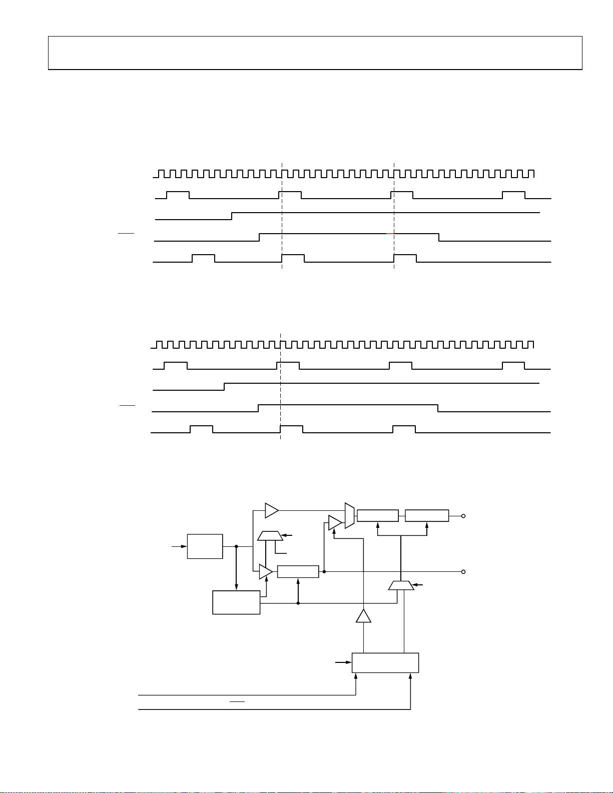
Data Sheet AD9558
A
A
A
M3b DIVIDER/OUT5 PROGRAMMING IN FRAME SYNCHRONIZATION MODE
In frame synchronization mode, the clock distribution signal path
for OUT5 is changed, as follows: the OUT5 signal goes from the RF
divider to the M0 divider, and then to the M3 and M3b dividers.
This means that in frame synchronization mode, the total divide
ratio between the RF divider and OUT5 is M0 × M3 × M3b.
The other important change is that the sync signal for the M3b
divider is no longer the standard clock distribution sync. It is
controlled by a signal derived from the input frame pulse.
CTIVE SYNC
OUPUT CLOCK
(OUT0)
FRAME CLOCK INPUT
(REFC/REFD)
(REGIST ER 0x0640[0] = 1b)
(REGISTER OR SYNC PIN)
ENABLE Fsync
FRAME SY NC ARM
FRAME CLOCK
(OUT5)
NOTES
1. AFTER THE FRAME SYNC IS ARMED, THE FRAME CLOCK OUTPUT IS SYNCHRONIZED TO THE FRAME CLOCK INPUT.
THE SKEW BETWEE N THE FRAME CLOCK INPUT AND F RAME CLOCK OUTPUT I S 15ns (NOMINAL) P LUS A DELAY OF 0.5 T O 1.5 OUTPUT CLOCK CYCLES.
CTIVE S YNC
Figure 41. Frame Synchronization in Level Sensitive Mode
OUPUT CLOCK
(OUT0)
FRAME CL OCK INP UT
(REFC/REFD)
(REGIST ER 0x0640[0] = 1b)
(REGISTER OR SYNC PIN)
NOTES
1. AFTER THE F RAME SYNC IS ARMED, T HE FRAME CLOCK O UTPUT IS SYNCHRONIZED TO T HE FRAME CLOCK INPUT.
THE SKEW BETW EEN THE FRAME CL OCK INPUT AND FRAME CL OCK OUTPUT IS 15ns (NOMI NAL) PLUS 0.5 TO 1.5 OUT PUT CLOCK CYCLE S.
ENABLE Fsync
FRAME SYNC ARM
FRAME CLOCK
(OUT5)
CTIVE SYNC
Figure 42. Frame Synchronization in One Shot Mode
ENABLE Fsync
09758-141
09758-142
M3 DIVIDER
ENABLE
FROM
APLL
FRAME SYNC PULSE INPUT (ON REFC OR REFD)
Fsync_arm (FROM EITHER THE SYNC PIN OR THE Arm Soft Fsync BIT IN REGISTER 0x0641[0])
NOTES
1. THE ENABLE Fsync FUNCTI ON IN THE DI AGRAM IS CO NTROLL ED BY REGIS TER 0x0640[0].
RF
DIVIDER 1
CLOCK
DISTRIBUT ION
SYNC LOG IC
Figure 43. Frame Synchronization Implementation
Fsync
LOGIC 0
M0 DIVIDER
ENABLE Fsync
OUTPUT
SYNC
LEVEL
(RETIMED)
DELAY
FRAME SYNC
PULSE GENERATOR
M3b DIVI DER
ENABLE Fsync
OUTPUT
SYNC
PULSE
OUT5
OUT0
09758-143
Rev. A | Page 41 of 104

AD9558 Data Sheet
STATUS AND CONTROL
MULTIFUNCTION PINS (M7 TO M0)
The AD9558 has eight digital CMOS I/O pins (M7 to M0)
that are configurable for a variety of uses. To use these
functions, the user must enable them by writing a 0x01 to
Register 0x0200. The function of these pins is programmable via
the register map. Each pin can control or monitor an assortment
of internal functions based on the contents of Register 0x0201 to
Register 0x0208.
To monitor an internal function with a multifunction pin, write
a Logic 1 to the most significant bit of the register associated
with the desired multifunction pin. The value of the seven least
significant bits of the register defines the control function, as
shown in Table 129.
To control an internal function with a multifunction pin, write a
Logic 0 to the most significant bit of the register associated with
the desired multifunction pin. The monitored function depends
on the value of the seven least significant bits of the register, as
shown in Table 130.
If more than one multifunction pin operates on the same
control signal, then internal priority logic ensures that only one
multifunction pin serves as the signal source. The selected pin is
the one with the lowest numeric suffix. For example, if both M0
and M3 operate on the same control signal, then M0 is used as
the signal source and the redundant pins are ignored.
At power-up, the multifunction pins can be used to force the
device into certain configurations as defined in the initial pin
programming section. This functionality, however, is valid only
during power-up or following a reset, after which the pins can
be reconfigured via the serial programming port or via the
EEPROM.
If the output SYNC function is to be controlled using an M pin,
1. First, enable the M pins by writing Register 0x0200 = 0x01.
2. Issue an I/O update (Register 0x0005 = 0x01).
3. Set the appropriate M pin function.
If this process is not followed, a SYNC pulse is issued automatically.
IRQ Pin
The AD9558 has a dedicated interrupt request (IRQ) pin.
Bits[1:0] of the IRQ pin output mode register (Register 0x0209)
control how the IRQ pin asserts an interrupt based on the value
of the two bits, as follows:
00—The IRQ pin is high impedance when deasserted and active
low when asserted and requires an external pull-up resistor.
01—The IRQ pin is high impedance when deasserted and active
high when asserted and requires an external pull-down
resistor.
10—The IRQ pin is Logic 0 when deasserted and Logic 1 when
asserted.
11—The IRQ pin is Logic 1 when deasserted and Logic 0 when
asserted. (This is the default operating mode.)
The AD9558 asserts the IRQ pin when any bit in the IRQ monitor
register (Address 0x0D02 to Address 0x0D07) is a Logic 1. Each
bit in this register is associated with an internal function that is
capable of producing an interrupt. Furthermore, each bit of the
IRQ monitor register is the result of a logical AND of the associated
internal interrupt signal and the corresponding bit in the IRQ
mask register (Address 0x020A to Address 0x020E). That is, the
bits in the IRQ mask register have a one-to-one correspondence
with the bits in the IRQ monitor register. When an internal
function produces an interrupt signal and the associated IRQ
mask bit is set, the corresponding bit in the IRQ monitor register
is set. The user should be aware that clearing a bit in the IRQ
mask register removes only the mask associated with the
internal interrupt signal. It does not clear the corresponding bit
in the IRQ monitor register.
The IRQ pin is the result of a logical OR of all the IRQ monitor
register bits. Thus, the AD9558 asserts the IRQ pin as long as
any IRQ monitor register bit is a Logic 1. Note that it is possible
to have multiple bits set in the IRQ monitor register. Therefore,
when the AD9558 asserts the IRQ pin, it may indicate an interrupt
from several different internal functions. The IRQ monitor
register provides the user with a means to interrogate the
AD9558 to determine which internal function produced the
interrupt.
Typically, when the IRQ pin is asserted, the user interrogates
the IRQ monitor register to identify the source of the interrupt
request. After servicing an indicated interrupt, the user should
clear the associated IRQ monitor register bit via the IRQ
clearing register (Address 0x0A04 to Address 0x0A09). The bits
in the IRQ clearing register have a one-to-one correspondence with
the bits in the IRQ monitor register. Note that the IRQ clearing
register is autoclearing. The IRQ pin remains asserted until the
user clears all of the bits in the IRQ monitor register that
indicate an interrupt.
It is also possible to collectively clear all of the IRQ monitor
register bits by setting the clear all IRQs bit in the reset function
register (Register 0x0A03, Bit 1). Note that this is an autoclearing
bit. Setting this bit results in deassertion of the IRQ pin.
Alternatively, the user can program any of the multifunction
pins to clear all IRQs. This allows the user to clear all IRQs by
means of a hardware pin rather than by using a serial I/O port
operation.
Rev. A | Page 42 of 104
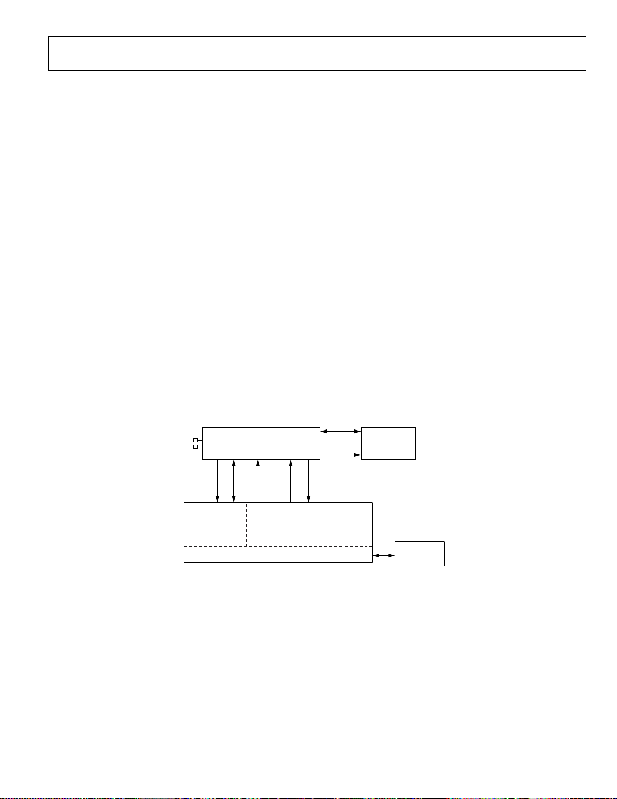
Data Sheet AD9558
A
WATCHDOG TIMER
The watchdog timer is a general purpose programmable timer.
To set the timeout period, the user writes to the 16-bit watchdog
timer register (Address 0x0210 to Address 0x0211). A value of
0b in this register disables the timer. A nonzero value sets the
timeout period in milliseconds (ms), giving the watchdog timer
a range of 1 ms to 65.535 sec. The relative accuracy of the timer
is approximately 0.1% with an uncertainty of 0.5 ms.
If enabled, the timer runs continuously and generates a timeout
event when the timeout period expires. The user has access to
the watchdog timer status via the IRQ mechanism and the
multifunction pins (M7 to M0). In the case of the multifunction
pins, the timeout event of the watchdog timer is a pulse that lasts
32 system clock periods.
There are two ways to reset the watchdog timer (thereby
preventing it from causing a timeout event). The first is by
writing a Logic 1 to the autoclearing clear watchdog bit in the
reset functions register (Register 0x0A03, Bit 0). Alternatively,
the user can program any of the multifunction pins to reset the
watchdog timer. This allows the user to reset the timer by means
of a hardware pin rather than by using a serial I/O port operation.
M3
M2
EEPROM
CONTROLLER
EEPROM
EEPROM Overview
The AD9558 contains an integrated 2048-byte, electrically
erasable, programmable read-only memory (EEPROM).
The AD9558 can be configured to perform a download at
power-up via the multifunction pins (M3 and M2), but uploads
and downloads can also be done on demand via the EEPROM
control registers (Address 0x0E00 to Address 0x0E03).
The EEPROM provides the ability to upload and download
configuration settings to and from the register map. Figure 44
shows a functional diagram of the EEPROM.
Register 0x0E10 to Register 0x0E3F represent a 53-byte EEPROM
storage sequence area (referred to as the “scratch pad” in this
section) that enables the user to store a sequence of instructions
for transferring data to the EEPROM from the device settings
portion of the register map. Note that the default values for
these registers provide a sample sequence for saving/retrieving
all of the AD9558 EEPROM-accessible registers. Figure 44 shows
the connectivity between the EEPROM and the controller that
manages data transfer between the EEPROM and the register map.
The controller oversees the process of transferring EEPROM data
to and from the register map. There are two modes of operation
handled by the controller: saving data to the EEPROM (upload
mode) or retrieving data from the EEPROM (download mode).
In either case, the controller relies on a specific instruction set.
DAT
EEPROM
ADDRESS
POINTER
EEPROM
(0x000 TO 0x1FF)
DEVICE
SETTINGS
ADDRESS
POINTER
DEVICE
SETTINGS
(0x0004 TO 0x0A0D)
DATA
(EEPROM STORAGE SEQUENCE)
(0E01 [3:0])
CONDITION
REGISTER MAP
Figure 44. EEPROM Functional Diagram
SCRATCH PAD
ADDRESS
DATA
POIN TER
SCRATCH PAD
(0x0E10 TO 0x0E45)
SERIAL
INPUT/OUTPUT
PORT
09758-024
Rev. A | Page 43 of 104

AD9558 Data Sheet
Table 21. EEPROM Controller Instruction Set
Instruction
Value (Hex)
0x00 to 0x7F Data 3
0x80 I/O update 1
0xA0 Calibrate 1
0xA1 Distribution sync 1
0xB0 to 0xCF Condition 1
0xFE Pause 1
0xFF End 1
Instruction Type
EEPROM Instructions
Tabl e 21 lists the EEPROM controller instruction set. The
controller recognizes all instruction types whether it is in
upload or download mode, except for the pause instruction,
which is recognized only in upload mode.
The I/O update, calibrate, distribution sync, and end instructions are mostly self-explanatory. The others, however, warrant
further detail, as described in the following paragraphs.
Data instructions are those that have a value from 0x000 to
0x7FF. A data instruction tells the controller to transfer data
between the EEPROM and the register map. The controller
requires the following two parameters to carry out the data
transfer:
• The number of bytes to transfer
• The register map target address
The controller decodes the number of bytes to transfer directly
from the data instruction itself by adding one to the value of the
instruction. For example, the 1A data instruction has a decimal
value of 26; therefore, the controller knows to transfer 27 bytes
(one more than the value of the instruction). When the
controller encounters a data instruction, it knows to read the
next two bytes in the scratch pad because these contain the
register map target address.
Bytes
Required
Description
A data instruction tells the controller to transfer data to or from the device settings
part of the register map. A data instruction requires two additional bytes that
together, indicate a starting address in the register map. Encoded in the data
instruction is the number of bytes to transfer, which is one more than the
instruction value.
When the controller encounters this instruction while downloading from the
EEPROM, it issues a soft I/O update.
When the controller encounters this instruction while downloading from the
EEPROM, it initiates a system clock calibration sequence.
When the controller encounters this instruction while downloading from the
EEPROM, it issues a sync pulse to the output distribution synchronization.
B1 to CF are condition instructions and correspond to Condition 1 through
Condition 31, respectively. B0 is the null condition instruction. See the EEPROM
Conditional Processing section for details.
When the controller encounters this instruction in the EEPROM storage sequence
area while uploading to the EEPROM, it holds both the scratch pad address pointer
and the EEPROM address pointer at its last value. This allows storage of more than
one instruction sequence in the EEPROM. Note that the controller does not copy
this instruction to the EEPROM during upload.
When the controller encounters this instruction in the the EEPROM storage
sequence area while uploading to the EEPROM, it resets both the register area
address pointer and the EEPROM address pointer and then enters an idle state.
When the controller encounters this instruction while downloading from the
EEPROM, it resets the EEPROM address pointer and then enters an idle state.
Note that, in the EEPROM scratch pad, the two registers that
comprise the address portion of a data instruction have the
MSB of the address in the D7 position of the lower register
address. The bit weight increases from left to right, from the
lower register address to the higher register address. Furthermore,
the starting address always indicates the lowest numbered
register map address in the range of bytes to transfer. That is,
the controller always starts at the register map target address
and counts upward regardless of whether the serial I/O port is
operating in I
2
C, SPI LSB-first, or SPI MSB-first mode.
As part of the data transfer process during an EEPROM upload,
the controller calculates a 1-byte checksum and stores it as the
final byte of the data transfer. As part of the data transfer process
during an EEPROM download, however, the controller again
calculates a 1-byte checksum value but compares the newly
calculated checksum with the one that was stored during the
upload process. If an upload/download checksum pair does not
match, the controller sets the EEPROM fault status bit. If the
upload/download checksums match for all data instructions
encountered during a download sequence, the controller sets
the EEPROM complete status bit.
Condition instructions are those that have a value from B0 to
CF. The B1 to CF condition instructions represent Condition 1
to Condition 31, respectively. The B0 condition instruction is
special because it represents the null condition (see the
EEPROM Conditional Processing section).
Rev. A | Page 44 of 104

Data Sheet AD9558
A pause instruction, like an end instruction, is stored at the
end of a sequence of instructions in the scratch pad. When the
controller encounters a pause instruction during an upload
sequence, it keeps the EEPROM address pointer at its last value.
This way the user can store a new instruction sequence in the
scratch pad and upload the new sequence to the EEPROM. The
new sequence is stored in the EEPROM address locations
immediately following the previously saved sequence. This
process is repeatable until an upload sequence contains an end
instruction. The pause instruction is also useful when used in
conjunction with condition processing. It allows the EEPROM
to contain multiple occurrences of the same registers, with each
occurrence linked to a set of conditions (see the EEPROM
Conditional Processing section).
EEPROM Upload
To upload data to the EEPROM, the user must first ensure that
the write enable bit (Register 0x0E00, Bit 0) is set. Then, on
setting the autoclearing save to EEPROM bit (Register 0x0E02,
Bit 0), the controller initiates the EEPROM data storage process.
Uploading EEPROM data requires that the user first write an
instruction sequence into the scratch pad registers. During the
upload process, the controller reads the scratch pad data byteby-byte, starting at Register 0x0E10 and incrementing the scratch
pad address pointer, as it goes, until it reaches a pause or end
instruction.
As the controller reads the scratch pad data, it transfers the
data from the scratch pad to the EEPROM (byte-by-byte) and
increments the EEPROM address pointer accordingly, unless
it encounters a data instruction. A data instruction tells the
controller to transfer data from the device settings portion of
the register map to the EEPROM. The number of bytes to transfer
is encoded within the data instruction, and the starting address
for the transfer appears in the next two bytes in the scratch pad.
When the controller encounters a data instruction, it stores the
instruction in the EEPROM, increments the EEPROM address
pointer, decodes the number of bytes to be transferred, and
increments the scratch pad address pointer. Then it retrieves the
next two bytes from the scratch pad (the target address) and
increments the scratch pad address pointer by 2. Next, the
controller transfers the specified number of bytes from the
register map (beginning at the target address) to the EEPROM.
When it completes the data transfer, the controller stores an extra
byte in the EEPROM to serve as a checksum for the transferred
block of data. To account for the checksum byte, the controller
increments the EEPROM address pointer by one more than the
number of bytes transferred. Note that, when the controller
transfers data associated with an active register, it actually
transfers the buffered contents of the register (refer to the
Buffered/Active Registers section for details on the difference
between buffered and active registers). This allows for the transfer
of nonzero autoclearing register contents.
Note that conditional processing (see the EEPROM Conditional
Processing section) does not occur during an upload sequence.
EEPROM Download
An EEPROM download results in data transfer from the
EEPROM to the device register map. To download data,
the user sets the autoclearing load from the EEPROM bit
(Register 0x0E03, Bit 1). This commands the controller to
initiate the EEPROM download process. During download, the
controller reads the EEPROM data byte-by-byte, incrementing
the EEPROM address pointer as it goes, until it reaches an end
instruction. As the controller reads the EEPROM data, it
executes the stored instructions, which includes transferring
stored data to the device settings portion of the register map
when it encounters a data instruction.
Note that conditional processing (see the EEPROM Conditional
Processing section) is applicable only when downloading.
Automatic EEPROM Download
Following a power-up, an assertion of the
reset (Register 0x0000, Bit 5 = 1), if the PINCONTROL pin is
low, and M3 and M2 are either high or low (see ), the
instruction sequence stored in the EEPROM executes automatically
with one of eight conditions. If M3 and M2 are left floating and
the PINCONTROL pin is low, the EEPROM is bypassed and
the factory defaults are used. In this way, a previously stored set
of register values downloads automatically on power-up or with
a hard or soft reset. See the
section for details regarding conditional processing and the way
it modifies the download process.
Table 22. EEPROM Setup
M3 M2 ID EEPROM Download?
Low Low 1 Yes, EEPROM Condition 1
Low Open 2 Yes, EEPROM Condition 2
Low High 3 Yes, EEPROM Condition 3
Open Low 4 Yes, EEPROM Condition 4
Open Open 0 No
Open High 5 Yes, EEPROM Condition 5
High Low 6 Yes, EEPROM Condition 6
High Open 7 Yes, EEPROM Condition 7
High High 8 Yes, EEPROM Condition 8
EEPROM Conditional Processing
RESET
pin, or a soft
Tabl e 22
Rev. A | Page 45 of 104

AD9558 Data Sheet
EEPROM Conditional Processing
The condition instructions allow conditional execution of
EEPROM instructions during a download sequence. During
an upload sequence, however, they are stored as is and have
no effect on the upload process.
Note that, during EEPROM downloads, the condition instructions
themselves and the end instruction always execute unconditionally.
Conditional processing makes use of two elements: the condition
(from Condition 1 to Condition 8) and the condition tag board.
The relationships among the condition, the condition tag board,
and the EEPROM controller appear schematically in Figure 45.
The condition is a 4-bit value with 16 possibilities. Condition = 0
is the null condition. When the null condition is in effect, the
EEPROM controller executes all instructions unconditionally.
Condition 9 through Condition 15 are not accessible using the
M pins. The remaining eight possibilities (that is, Condition = 1
through Condition = 8) modify the EEPROM controller’s
handling of a download sequence. The condition originates
from one of two sources (see Figure 45), as follows:
• FncInit, Bits[3:0], which is the state of the M2 and M3
multifunction pins at power-up (see Tab le 2 2)
• Register 0x0E01, Bits[3:0]
If Register 0x0E01, Bits[3:0] ≠ 0, then the condition is the value
that is stored in Register 0x0E01, Bits[3:0]; otherwise, the condition
is FncInit, Bits[3:0]. Note that a nonzero condition that is present
in Register 0x0E01, Bits[3:0] takes precedence over FncInit,
Bits[3:0].
The condition tag board is a table maintained by the EEPROM
controller. When the controller encounters a condition instruction, it decodes the B1 through CF instructions as Condition = 1
through Condition = 8, respectively, and tags that particular
condition in the condition tag board. However, the B0 condition
instruction decodes as the null condition, for which the controller
clears the condition tag board; and subsequent download
instructions execute unconditionally (until the controller
encounters a new condition instruction).
During download, the EEPROM controller executes or skips
instructions depending on the value of the condition and the
contents of the condition tag board. Note, however, that the
condition instructions and the end instruction always execute
unconditionally during download. If condition = 0, then all
instructions during download execute unconditionally. If
Condition ≠ 0 and there are any tagged conditions in the condition
tag board, then the controller executes instructions only if the
condition is tagged. If the condition is not tagged, then the
controller skips instructions until it encounters a condition
instruction that decodes as a tagged condition. Note that the
condition tag board allows for multiple conditions to be tagged
at any given moment. This conditional processing mechanism
enables the user to have one download instruction sequence
with many possible outcomes depending on the value of the
condition and the order in which the controller encounters
condition instructions.
EEPROM
STORE CONDITION
INSTRUCT IONS AS
THEY ARE READ FROM
THE SCRATCH PAD.
SCRATCH
PAD
EXAMPLE
CONDIT ION 3 AND
CONDITION 13
ARE TAGGED
IF B1 ≤ INSTRUCTION ≤ CF,
THEN TAG DECODED CO NDITI ON
WATCH FOR
OCCURRENCE OF
CONDITI ON
INSTRUCT IONS
DURING
DOWNLO AD.
UPLOAD
PROCEDURE
EEPROM CONTROLLER
PROCEDURE
Figure 45. EEPROM Conditional Processing
25 26 27 28 29
CONDITION
HANDLER
DOWNLO AD
CONDITION
TAG BO ARD
1 65432
111098
IF INSTRUCTION = B0,
THEN CLEAR ALL TAGS
EXECUT E/SKIP
INST RUCT ION(S)
7
15141312
2322212019181716
30 3124
REGISTER
0x0E01, BITS[3:0]
4 4
IF {0E01, BITS[3:0] ≠ 0}
CONDIT ION = 0E01
ELSE
CONDIT ION = Fn cInit,
ENDIF
IF {NO TAGS} OR {CONDITION = 0}
EXECUTE I NSTRUCTI ONS
ELSE
IF {CONDITION ISTAGGED}
EXECUTE INSTRUCTIONS
ELSE
SKIP INSTRUCTIONS
ENDIF
ENDIF
M3 AND M2 PINS
(3-LEVEL LOGIC)
FncInit, BITS[3:0]
, BITS[3:0]
BITS[3:0]
4
CONDITION
09758-025
Rev. A | Page 46 of 104

Data Sheet AD9558
Tabl e 23 lists a sample EEPROM download instruction sequence.
It illustrates the use of condition instructions and how they alter
the download sequence. The table begins with the assumption
that no conditions are in effect. That is, the most recently executed
condition instruction is either B0 or no conditional instructions
have been processed.
Table 23. EEPROM Conditional Processing Example
Instruction Action
0x08
0x01
0x00
0xB1 Tag Condition 1.
0x19
0x04
0x00
0xB2 Tag Condition 2.
0xB3 Tag Condition 3.
0x07
0x05
0x00
0x0A
0xB0 Clear the tag condition board.
0x80
0x0A
Transfer the system clock register contents,
regardless of the current condition.
Transfer the clock distribution register contents
only if tag condition = 1.
Transfer the reference input register contents only
if tag condition = 1, 2, or 3.
Calibrate the system clock only if tag condition =
1, 2, or 3.
Execute an I/O update, regardless of the value of
the tag condition.
Calibrate the system clock, regardless of the value
of the tag condition.
Storing Multiple Device Setups in EEPROM
Conditional processing makes it possible to create a number of
different device setups, store them in EEPROM, and download
a specific setup on demand. To do so, first program the device
control registers for a specific setup. Then, store an upload
sequence in the EEPROM scratch pad with the following
general form:
1. Condition instruction (B1 to CF) to identify the setup with
a specific condition (1 to 31)
2. Data instructions (to save the register contents) along with
any required calibrate and/or I/O update instructions
3. Pause instruction (FE)
Reprogram the device control registers for the next desired
setup. Then store a new upload sequence in the EEPROM
scratch pad with the following general form:
1. Condition instruction (B0)
2. The next desired condition instruction (B1 to CF, but
different from the one used during the previous upload to
identify a new setup)
3. Data instructions (to save the register contents) along with
any required calibrate and/or I/O update instructions
4. Pause instruction (FE)
With the upload sequence written to the scratch pad, perform
an EEPROM upload (Register 0x0E02, Bit 0).
Repeat the process of programming the device control registers
for a new setup, storing a new upload sequence in the EEPROM
scratch pad (Step 1 through Step 4), and executing an EEPROM
upload (Register 0x0E02, Bit 0) until all of the desired setups
have been uploaded to the EEPROM.
Note that, on the final upload sequence stored in the scratch
pad, the pause instruction (FE) must be replaced with an end
instruction (FF).
To download a specific setup on demand, first store the condition
associated with the desired setup in Register 0x0E01, Bits[4:0].
Then perform an EEPROM download (Register 0x0E03, Bit 1).
Alternatively, to download a specific setup at power-up, apply
the required logic levels necessary to encode the desired condition
on the M2 and M3 multifunction pins. Then power up the device;
an automatic EEPROM download occurs. The condition (as
established by the M2 and M3 multifunction pins) guides the
download sequence and results in a specific setup.
Keep in mind that the number of setups that can be stored
in the EEPROM is limited. The EEPROM can hold a total of
2048 bytes. Each nondata instruction requires one byte of
storage. Each data instruction, however, requires N + 4 bytes of
storage, where N is the number of transferred register bytes and
the other four bytes include the data instruction itself (one
byte), the target address (two bytes), and the checksum
calculated by the EEPROM controller during the upload
sequence (one byte).
With the upload sequence written to the scratch pad, perform
an EEPROM upload (Register 0x0E02, Bit 0).
Rev. A | Page 47 of 104

AD9558 Data Sheet
Programming the EEPROM to Configure an M Pin to Control Synchronization of Clock Distribution
A special EEPROM loading sequence is required to use the
EEPROM to load the registers and to use an M pin to
enable/disable outputs.
To control the output sync function by using an M pin, perform
the following steps:
1. Enable the M pins by writing Register 0x0200 = 0x01.
2. Issue an I/O update (Register 0x0005 = 0x01).
3. Set the appropriate M pin function (see the Clock
Distribution Synchronization section for details).
If this sequence is not performed, a SYNC pulse is issued
automatically.
The following changes write Register 0x0200 first and then issue
an I/O update before writing the remaining M pin configuration
registers in Register 0x0201 to Register 0x0208.
The default EEPROM loading sequence from Register 0x0E10 to
Register 0x0E16 is unchanged. The following steps must be
inserted into the EEPROM storage sequence:
1. R0x0E17 = 0x00 # Write one byte
2. R0x0E18 = 0x02 # at Register 0x0200
3. R0x0E19 = 0x00 #
4. R0x0E1A = 0x80 # Op code for I/O
Update R0x0E1B = 0x10 # Transfer 17 instead of 18 bytes
5. R0x0E1C = 0x02 # Transfer starts at Register address
6. R0x0E1D = 0x01 # 0x0201 instead of 0x0200
The rest of the EEPROM loading sequence is the same as the
default EEPROM loading sequence, except that the register
address of the EEPROM storage sequence is shifted down four
bytes from the default. For example,
• R0x0E1E = default value of Register 0x0E1A = 0x2E
• R0x0E1F = default value of Register 0x0E1B = 0x03
• R0x0E20 = default value of Register 0x0E1C = 0x00
• …
• R0x0E40 = default value of Register 0x0E1C = 0x3C = 0xFF
(end of data)
Rev. A | Page 48 of 104

Data Sheet AD9558
SERIAL CONTROL PORT
The AD9558 serial control port is a flexible, synchronous serial
communications port that provides a convenient interface to
many industry-standard microcontrollers and microprocessors.
The AD9558 serial control port is compatible with most
synchronous transfer formats, including IC, Motorola SPI, and
Intel SSR protocols. The serial control port allows read/write
access to the AD9558 register map.
In SPI mode, single or multiple byte transfers are supported.
The SPI port configuration is programmable via Register 0x0000.
This register is integrated into the SPI control logic rather than
in the register map and is distinct from the I
2
C Register 0x0000.
It is also inaccessible to the EEPROM controller.
Although the AD9558 supports both the SPI and I
2
C serial port
protocols, only one or the other is active following power-up (as
determined by the M0 and M1 multifunction pins during the
startup sequence). That is, the only way to change the serial port
protocol is to reset the device (or cycle the device power supply).
SPI/I²C PORT SELECTION
Because the AD9558 supports both SPI and IC protocols, the
active serial port protocol depends on the logic state of the
PINCONTROL, M1, and M0 pins. The PINCONTROL pin
must be low, and the state of the M0 and M1 pins determines
2
the I
C address, or if SPI mode is enabled. See Tab le 2 4 for the
2
I
C address assignments.
Table 24. SPI/IC Serial Port Setup
M1 M0 SPI/I²C
Low Low SPI
Low Open I²C, 1101000
Low High I²C, 1101001
Open Low I²C, 1101010
Open Open I²C, 1101011
Open High I²C, 1101100
High Low I²C, 1101101
High Open I²C, 1101110
High High I²C, 1101111
SPI SERIAL PORT OPERATION
Pin Descriptions
The SCLK (serial clock) pin serves as the serial shift clock. This
pin is an input. SCLK synchronizes serial control port read and
write operations. The rising edge SCLK registers write data bits,
and the falling edge registers read data bits. The SCLK pin
supports a maximum clock rate of 40 MHz.
The SDIO (serial data input/output) pin is a dual-purpose pin
and acts as either an input only (unidirectional mode) or as
both an input and an output (bidirectional mode). The AD9558
default SPI mode is bidirectional.
The SDO (serial data output) pin is useful only in unidirectional
I/O mode. It serves as the data output pin for read operations.
CS
The
(chip select) pin is an active low control that gates read
and write operations. This pin is internally connected to a 30 kΩ
pull-up resistor. When
CS
is high, the SDO and SDIO pins go
into a high impedance state.
SPI Mode Operation
The SPI port supports both 3-wire (bidirectional) and 4-wire
(unidirectional) hardware configurations and both MSB-first
and LSB-first data formats. Both the hardware configuration
and data format features are programmable. By default, the
AD9558 uses the bidirectional MSB-first mode. The reason that
bidirectional is the default mode is so that the user can still
write to the device, if it is wired for unidirectional operation, to
switch to unidirectional mode.
Assertion (active low) of the
operation to the SPI port. For data transfers of three
AD9558
CS
pin initiates a write or read
bytes or fewer (excluding the instruction word), the device
supports the
CS
the
CS
stalled high mode (see ). In this mode,
Tabl e 25
pin can be temporarily deasserted on any byte boundary,
allowing time for the system controller to process the next byte.
CS
can be deasserted only on byte boundaries, however. This
applies to both the instruction and data portions of the transfer.
During stall high periods, the serial control port state machine
enters a wait state until all data is sent. If the system controller
decides to abort a transfer midstream, then the state machine must
be reset either by completing the transfer or by asserting the
CS
pin for at least one complete SCLK cycle (but less than eight
SCLK cycles). Deasserting the
CS
pin on a nonbyte boundary
terminates the serial transfer and flushes the buffer.
In streaming mode (see Ta b le 2 5), any number of data bytes can
be transferred in a continuous stream. The register address is
automatically incremented or decremented.
CS
must be deasserted
at the end of the last byte that is transferred, thereby ending the
streaming mode.
Table 25. Byte Transfer Count
W1 W0 Bytes to Transfer
0 0 1
0 1 2
1 0 3
1 1 Streaming mode
Communication Cycle—Instruction Plus Data
The SPI protocol consists of a two-part communication cycle.
The first part is a 16-bit instruction word that is coincident with
the first 16 SCLK rising edges and a payload. The instruction
word provides the AD9558 serial control port with information
regarding the payload. The instruction word includes the R/
W
bit that indicates the direction of the payload transfer (that is, a
read or write operation). The instruction word also indicates
the number of bytes in the payload and the starting register
address of the first payload byte.
Rev. A | Page 49 of 104

AD9558 Data Sheet
Write
If the instruction word indicates a write operation, the payload
is written into the serial control port buffer of the AD9558. Data
bits are registered on the rising edge of SCLK. The length of the
transfer (1, 2, or 3 bytes or streaming mode) depends on the W0
and W1 bits (see Ta bl e 25 ) in the instruction byte. When not
streaming,
bits to stall the bus (except after the last byte, where it ends the
cycle). When the bus is stalled, the serial transfer resumes when
CS
is asserted. Deasserting the CS pin on a nonbyte boundary
resets the serial control port. Reserved or blank registers are not
skipped over automatically during a write sequence. Therefore,
the user must know what bit pattern to write to the reserved
registers to preserve proper operation of the part. Generally, it
does not matter what data is written to blank registers, but it is
customary to write 0s.
Most of the serial port registers are buffered (refer to the
Buffered/Active Registers section for details on the difference
between buffered and active registers). Therefore, data written into
buffered registers does not take effect immediately. An
additional operation is required to transfer buffered serial
control port contents to the registers that actually control the
device. This is accomplished with an I/O update operation,
which is performed in one of two ways. One is by writing a
Logic 1 to Register 0x0005, Bit 0 (this bit is autoclearing). The
other is to use an external signal via an appropriately
programmed multifunction pin. The user can change as many
register bits as desired before executing an I/O update. The I/O
update operation transfers the buffer register contents to their
active register counterparts.
CS
can be deasserted after each sequence of eight
Read
The AD9558 supports the long instruction mode only. If the
instruction word indicates a read operation, the next N × 8
SCLK cycles clock out the data from the address specified in the
instruction word. N is the number of data bytes read and
depends on the W0 and W1 bits of the instruction word. The
readback data is valid on the falling edge of SCLK. Blank
registers are not skipped over during readback.
A readback operation takes data from either the serial control
port buffer registers or the active registers, as determined by
Register 0x0004, Bit 0.
SPI Instruction Word (16 Bits)
The MSB of the 16-bit instruction word is R/W, which indicates
whether the instruction is a read or a write. The next two bits, W1
and W0, indicate the number of bytes in the transfer (see ). Tab le 2 5
The final 13 bits are the register address (A12 to A0), which
indicates the starting register address of the read/write operation
(see Tabl e 27 ).
SPI MSB-/LSB-First Transfers
The AD9558 instruction word and payload can be MSB first or
LSB first. The default for the AD9558 is MSB first. The LSB-first
mode can be set by writing a 1 to Register 0x0000, Bit 6.
Immediately after the LSB-first bit is set, subsequent serial
control port operations are LSB first.
When MSB-first mode is active, the instruction and data bytes
must be written from MSB to LSB. Multibyte data transfers in
MSB-first format start with an instruction byte that includes the
register address of the most significant payload byte. Subsequent
data bytes must follow in order from high address to low
address. In MSB-first mode, the serial control port internal
address generator decrements for each data byte of the multibyte transfer cycle.
When Register 0x0000, Bit 6 = 1 (LSB first), the instruction and
data bytes must be written from LSB to MSB. Multibyte data
transfers in LSB-first format start with an instruction byte that
includes the register address of the least significant payload byte
followed by multiple data bytes. The serial control port internal
byte address generator increments for each byte of the multibyte
transfer cycle.
For multibyte MSB-first (default) I/O operations, the serial
control port register address decrements from the specified
starting address toward Address 0x0000. For multibyte LSB-first
I/O operations, the serial control port register address
increments from the starting address toward Address 0x1FFF.
Reserved addresses are not skipped during multibyte I/O
operations; therefore, the user should write the default value to
a reserved register and 0s to unmapped registers. Note that it is
more efficient to issue a new write command than to write the
default value to more than two consecutive reserved (or
unmapped) registers.
Table 26. Streaming Mode (No Addresses Are Skipped)
Write Mode Address Direction Stop Sequence
LSB First Increment 0x0000 ... 0x1FFF
MSB First Decrement 0x1FFF ... 0x0000
Table 27. Serial Control Port, 16-Bit Instruction Word, MSB First
MSB LSB
I15 I14 I13 I12 I11 I10 I9 I8 I7 I6 I5 I4 I3 I2 I1 I0
R/W
W1 W0 A12 A11 A10 A9 A8 A7 A6 A5 A4 A3 A2 A1 A0
Rev. A | Page 50 of 104
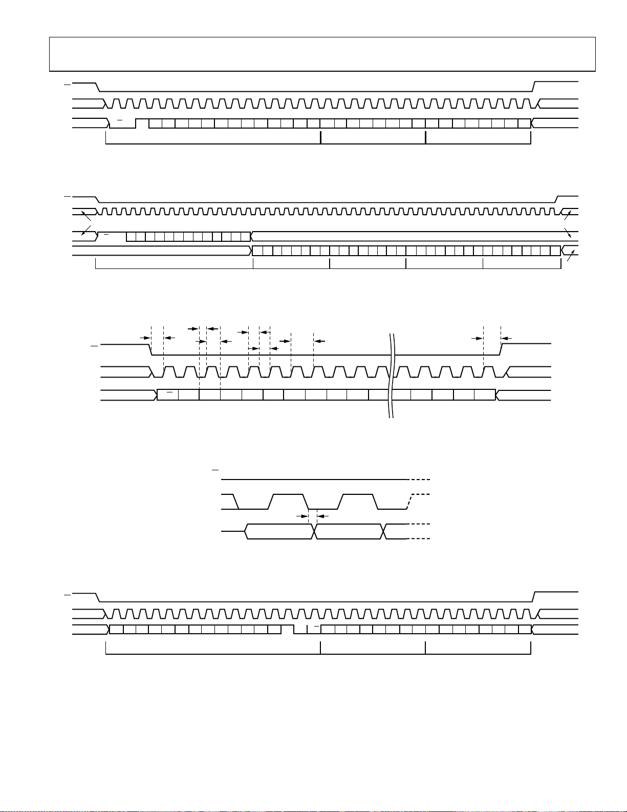
Data Sheet AD9558
CS
DON'T CARE
SCLK
DON'T CARE
DON'T CARE
SDIO A12W0W1R/W A11 A10 A9 A8 A7 A6 A5 A4 A3 A2 A1 A0 D7 D6 D5 D4 D3 D2 D1 D0 D7 D6 D5 D4 D3 D2 D1 D0
16-BIT INST RUCTION HEADER REGISTER (N) DATA REGISTER (N – 1) DATA
Figure 46. Serial Control Port Write—MSB First, 16-Bit Instruction, Two Bytes of Data
CS
SCLK
DON'T CARE
SDIO
SDO
DON'T CARE
A12W0W1R/ W A11 A10 A9 A8 A7 A6 A5 A4 A3 A2 A1 A0
D7 D6 D5 D4 D3 D2 D1 D0 D7 D6 D5 D4 D3 D2 D1 D0 D7 D6 D5 D4 D3 D2 D1 D0 D7 D6 D5 D4 D3 D2 D1 D0
REGISTER (N) DATA16-BIT INST RUCTION HEADE R REGISTE R (N – 1) DATA REGISTER (N – 2) DAT A REGISTER (N – 3) DATA
Figure 47. Serial Control Port Read—MSB First, 16-Bit Instruction, Four Bytes of Data
t
SCLK
SDIO
CS
DON'T CARE
DON'T CARE
DS
t
S
R/W
t
DH
t
LOW
W1W0A12A11A10A9A8A7A6A5D4D3D2D1D0
t
HIGH
t
t
CLK
C
DON'T CARE
DON'T CARE
Figure 48. Serial Control Port Write—MSB First, 16-Bit Instruction, Timing Measurements
CS
DON'T CARE
DON'T CARE
DON'T
CARE
09758-031
09758-029
09758-030
SCLK
SDIO
CS
DON'T CARE
DON'T CARE
SCLK
t
SDIO
SDO
DV
DATA BIT N – 1DATA BIT N
09758-032
Figure 49. Timing Diagram for Serial Control Port Register Read
A0 A1 A2 A3 A4 A5 A6 A7 A8 A9 A10 A11 A12 D1D0R/WW1W0 D2 D3 D4 D5 D6 D7 D0 D1 D2 D3 D4 D5 D6 D7
16-BIT INST RUCTION HEADER REGISTER (N) DAT A REGISTER (N + 1) DATA
Figure 50. Serial Control Port Write—LSB First, 16-Bit Instruction, Two Bytes of Data
Rev. A | Page 51 of 104
DON'T CARE
DON'T CARE
09758-033

AD9558 Data Sheet
CS
SCLK
t
S
t
CLK
t
HIGH
t
DS
t
DH
t
LOW
t
C
SDIO
BIT N BIT N + 1
Figure 51. Serial Control Port Timing—Write
Table 28. Serial Control Port Timing
Parameter Description
tDS Setup time between data and the rising edge of SCLK
tDH Hold time between data and the rising edge of SCLK
t
Period of the clock
CLK
tS
tC
t
Minimum period that SCLK should be in a logic high state
HIGH
t
Minimum period that SCLK should be in a logic low state
LOW
t
SCLK to valid SDIO and SDO (see Figure 49)
DV
Setup time between the CS falling edge and the SCLK rising edge (start of the communication cycle)
Setup time between the SCLK rising edge and CS
rising edge (end of the communication cycle)
09758-034
Rev. A | Page 52 of 104
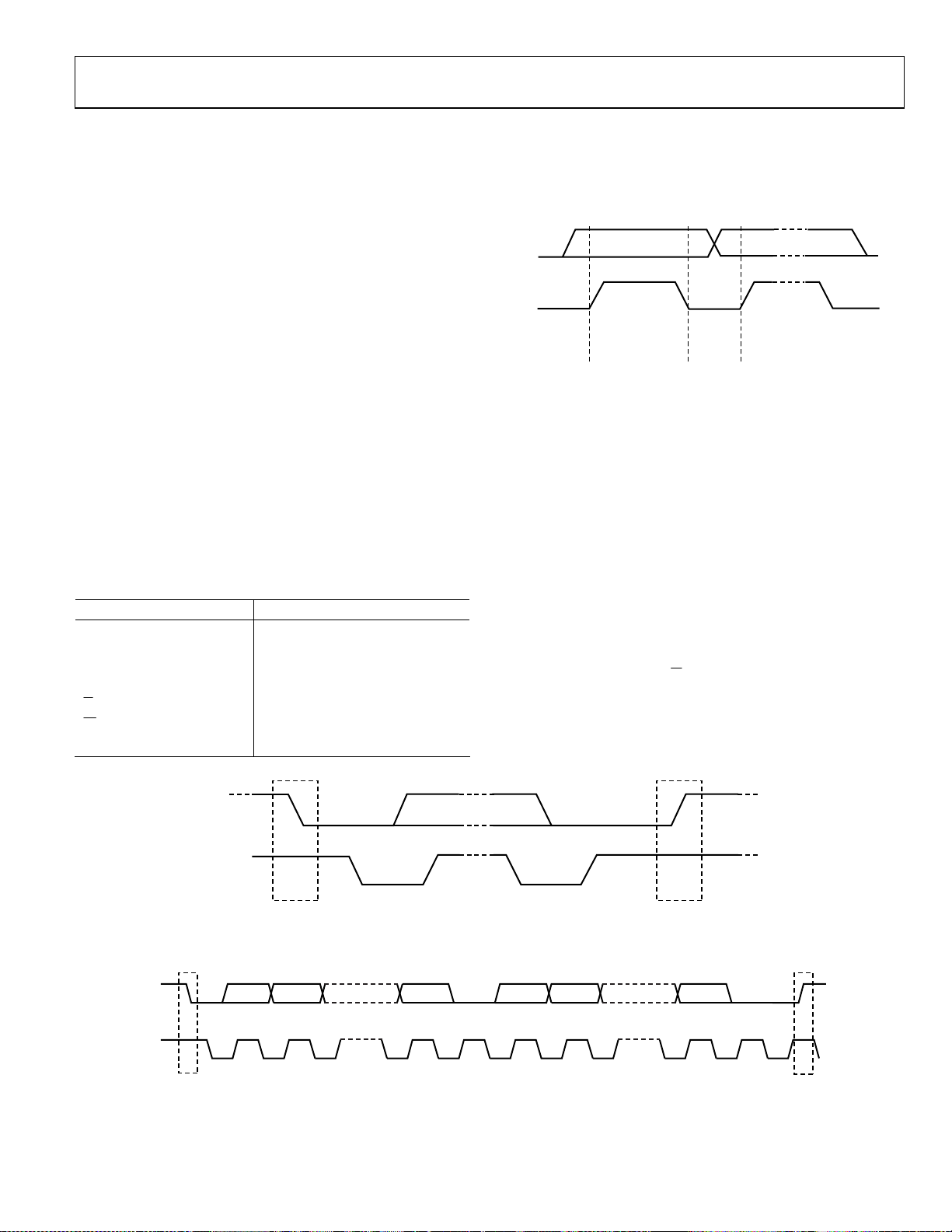
Data Sheet AD9558
A
A
I²C SERIAL PORT OPERATION
The I2C interface has the advantage of requiring only two control
pins and is a de facto standard throughout the I
However, its disadvantage is programming speed, which is
400 kbps maximum. The AD9558 IC port design is based on the
IC fast mode standard; therefore, it supports both the 100 kHz
standard mode and 400 kHz fast mode. Fast mode imposes a
glitch tolerance requirement on the control signals. That is, the
input receivers ignore pulses of less than 50 ns duration.
The AD9558 IC port consists of a serial data line (SDA) and a
serial clock line (SCL). In an IC bus system, the AD9558 is
connected to the serial bus (data bus SDA and clock bus SCL)
as a slave device; that is, no clock is generated by the AD9558.
The AD9558 uses direct 16-bit memory addressing instead of
traditional 8-bit memory addressing.
The AD9558 allows up to seven unique slave devices to occupy
2
the I
C bus. These are accessed via a 7-bit slave address that is
transmitted as part of an I
2
C packet. Only the device that has a
matching slave address responds to subsequent I
Tabl e 24 lists the supported device slave addresses.
I2C Bus Characteristics
A summary of the various I2C protocols appears in Tab le 2 9.
2
Table 29. I
C Bus Abbreviation Definitions
Abbreviation Definition
S Start
Sr Repeated start
P Stop
A Acknowledge
A
W
Nonacknowledge
Write
R Read
2
C industry.
2
C commands.
The transfer of data is shown in Figure 52. One clock pulse is
generated for each data bit transferred. The data on the SDA
line must be stable during the high period of the clock. The
high or low state of the data line can change only when the
clock signal on the SCL line is low.
SD
SCL
DATA LINE
STABLE;
DATA VALID
Figure 52. Valid Bit Transfer
CHANGE
OF DATA
ALLOWED
Start/stop functionality is shown in Figure 53. The start
condition is characterized by a high-to-low transition on the
SDA line while SCL is high. The start condition is always
generated by the master to initialize a data transfer. The stop
condition is characterized by a low-to-high transition on the
SDA line while SCL is high. The stop condition is always
generated by the master to terminate a data transfer. Every byte
on the SDA line must be eight bits long. Each byte must be
followed by an acknowledge bit; bytes are sent MSB first.
The acknowledge bit (A) is the ninth bit attached to any 8-bit
data byte. An acknowledge bit is always generated by the
receiving device (receiver) to inform the transmitter that the
byte has been received. It is done by pulling the SDA line low
during the ninth clock pulse after each 8-bit data byte.
The nonacknowledge bit (
A
) is the ninth bit attached to any 8bit data byte. A nonacknowledge bit is always generated by the
receiving device (receiver) to inform the transmitter that the
byte has not been received. It is done by leaving the SDA line
high during the ninth clock pulse after each 8-bit data byte.
09758-035
SDA
SCL
S
START CONDITION STOP CONDITION
Figure 53. Start and Stop Conditions
P
09758-036
SD
SCL
S
MSB
12
ACK FROM
SLAVE RE CEIVER
89
Figure 54. Acknowledge Bit
Rev. A | Page 53 of 104
12
ACK FROM
SLAVE RECEIVER
3 TO 73 TO 7 89
10
P
09758-037

AD9558 Data Sheet
A
A
Data Transfer Process
The master initiates data transfer by asserting a start condition.
This indicates that a data stream follows. All IC slave devices
connected to the serial bus respond to the start condition.
The master then sends an 8-bit address byte over the SDA line,
consisting of a 7-bit slave address (MSB first) plus an R/
W
A
E
A
bit.
This bit determines the direction of the data transfer, that is,
whether data is written to or read from the slave device (0 =
write, 1 = read).
The peripheral whose address corresponds to the transmitted
address responds by sending an acknowledge bit. All other
devices on the bus remain idle while the selected device waits
for data to be read from or written to it. If the R/
master (transmitter) writes to the slave device (receiver). If the
E
W
R/
A
A
bit is 1, the master (receiver) reads from the slave device
E
W
A
A
bit is 0, the
(transmitter).
The format for these commands is described in the Data Transfer
Format section.
Data is then sent over the serial bus in the format of nine clock
pulses, one data byte (eight bits) from either master (write mode)
or slave (read mode) followed by an acknowledge bit from the
receiving device. The number of bytes that can be transmitted
per transfer is unrestricted. In write mode, the first two data
bytes immediately after the slave address byte are the internal
memory (control registers) address bytes, with the high address
byte first. This addressing scheme gives a memory address of up
16
to 2
− 1 = 65,535. The data bytes after these two memory address
bytes are register data written to or read from the control registers.
In read mode, the data bytes after the slave address byte are
register data written to or read from the control registers.
When all data bytes are read or written, stop conditions are
established. In write mode, the master (transmitter) asserts
a stop condition to end data transfer during the 10
th
clock pulse
following the acknowledge bit for the last data byte from the slave
device (receiver). In read mode, the master device (receiver)
receives the last data byte from the slave device (transmitter) but
does not pull SDA low during the ninth clock pulse. This is known
as a nonacknowledge bit. By receiving the nonacknowledge bit,
the slave device knows that the data transfer is finished and
enters idle mode. The master then takes the data line low
during the low period before the 10
during the 10
th
clock pulse to assert a stop condition.
th
clock pulse, and high
A start condition can be used in place of a stop condition.
Furthermore, a start or stop condition can occur at any time,
and partially transferred bytes are discarded.
SD
SCL
S
MSB
12
ACK FROM
SLAVE RECEIVER
89
12
ACK FROM
SLAVE RECEIVER
3 TO 73 TO 7 8910
P
09758-038
Figure 55. Data Transfer Process (Master Write Mode, 2-Byte Transfer)
SD
SCL
ACK FROM
MASTER RECEIVER
S
12
89
12
3 TO 73 TO 7 8910
Figure 56. Data Transfer Process (Master Read Mode, 2-Byte Transfer)
NON-ACK FROM
MASTER RECEIVER
P
09758-039
Rev. A | Page 54 of 104
Data Sheet AD9558
SDA
Data Transfer Format
Write byte format—the write byte protocol is used to write a register address to the RAM starting from the specified RAM address.
S Slave
address
Send byte format—the send byte protocol is used to set up the register address for subsequent reads.
S Slave address
Receive byte format—the receive byte protocol is used to read the data byte(s) from RAM starting from the current address.
S Slave address R A RAM Data 0 A RAM Data 1 A RAM Data 2
Read byte format—the combined format of the send byte and the receive byte.
S Slave
Address
I²C Serial Port Timing
A RAM address
W
high byte
A RAM address high byte A RAM address low byte A P
W
A RAM
W
Address
High Byte
A RAM address
A RAM
Address
Low Byte
low byte
A Sr Slave
A RAM
Address
A RAM
Data 0
R A RAM
Data 0
Data 1
A RAM
Data 1
A RAM
Data 2
A RAM
Data 2
A P
P
A
A
P
t
t
F
SCL
SSr
LOW
t
HD; STA
t
R
t
HD; DAT
t
SU; DAT
t
F
t
t
HIGH
SU; STA
Figure 57. I²C Serial Port Timing
t
HD; STA
Table 30. IC Timing Definitions
Parameter Description
f
Serial clock
SCL
t
Bus free time between stop and start conditions
BUF
t
Repeated hold time start condition
HD; STA
t
Repeated start condition setup time
SU; STA
t
Stop condition setup time
SU; STO
t
Data hold time
HD; DAT
t
Date setup time
SU; DAT
t
SCL clock low period
LOW
t
SCL clock high period
HIGH
tR Minimum/maximum receive SCL and SDA rise time
tF Minimum/maximum receive SCL and SDA fall time
t
Pulse width of voltage spikes that must be suppressed by the input filter
SP
t
SP
t
SU; STO
t
R
t
BUF
P
S
09758-040
Rev. A | Page 55 of 104

AD9558 Data Sheet
PROGRAMMING THE I/O REGISTERS
The register map spans an address range from 0x0000 through
0x0E3C. Each address provides access to 1 byte (eight bits) of
data. Each individual register is identified by its four-digit
hexadecimal address (for example, Register 0x0A10). In some
cases, a group of addresses collectively defines a register.
In general, when a group of registers defines a control
parameter, the LSB of the value resides in the D0 position of the
register with the lowest address. The bit weight increases right
to left, from the lowest register address to the highest register
address.
Note that the EEPROM storage sequence registers (Address
0x0E10 to Address 0x0E3C) are an exception to the above
convention (see the EEPROM Instructions section).
BUFFERED/ACTIVE REGISTERS
There are two copies of most registers: buffered and active. The
value in the active registers is the one that is in use. The buffered
registers are the ones that take effect the next time the user
writes 0x01 to the I/O update register (Register 0x0005).
Buffering the registers allows the user to update a group of
registers (like the digital loop filter coefficients) at the same
time, which avoids the potential of unpredictable behavior in
the part. Registers with an L in the option column are live,
meaning that they take effect the moment the serial port
transfers that data byte.
AUTOCLEAR REGISTERS
An A in the option column of the register map identifies an
autoclear register. Typically, the active value for an autoclear
register takes effect following an I/O update. The bit is cleared
by the internal device logic upon completion of the prescribed
action.
REGISTER ACCESS RESTRICTIONS
Read and write access to the register map may be restricted
depending on the register in question, the source and direction
of access, and the current state of the device. Each register can
be classified into one or more access types. When more than
one type applies, the most restrictive condition is the one that
applies.
When access is denied to a register, all attempts to read the
register return a 0 byte, and all attempts to write to the register
are ignored. Access to nonexistent registers is handled in the
same way as for a denied register.
Regular Access
Registers with regular access do not fall into any other category.
Both read and write access to registers of this type can be from
either the serial ports or the EEPROM controller. However, only
one of these sources can have access to a register at any given
time (access is mutually exclusive). When the EEPROM controller
is active, in either load or store mode, it has exclusive access to
these registers.
Read-Only Access
An R in the option column of the register map identifies readonly registers. Access is available at all times, including when
the EEPROM controller is active. Note that read-only registers
(R) are inaccessible to the EEPROM, as well.
Exclusion from EEPROM Access
An E in the option column of the register map identifies a
register with contents that are inaccessible to the EEPROM.
That is, the contents of this type of register cannot be
transferred directly to the EEPROM or vice versa. Note that
read-only registers (R) are inaccessible to the EEPROM, as well.
Rev. A | Page 56 of 104

Data Sheet AD9558
THERMAL PERFORMANCE
Table 31. Thermal Parameters for the 64-Lead LFCSP Package
Symbol Thermal Characteristic Using a JEDEC51-7 Plus JEDEC51-5 2S2P Test Board1 Value2 Unit
θJA Junction-to-ambient thermal resistance, 0.0 m/sec airflow per JEDEC JESD51-2 (still air) 21.7 °C/W
θ
Junction-to-ambient thermal resistance, 1.0 m/sec airflow per JEDEC JESD51-6 (moving air) 18.9 °C/W
JMA
θ
Junction-to-ambient thermal resistance, 2.5 m/sec airflow per JEDEC JESD51-6 (moving air) 16.9 °C/W
JMA
θJB Junction-to-board thermal resistance, 0.0 m/sec airflow per JEDEC JESD51-8 (still air) 11.3 °C/W
θJC Junction-to-case thermal resistance (die-to-heat sink) per MIL-Std 883, Method 1012.1 1.2 °C/W
ΨJT Junction-to-top-of-package characterization parameter, 0 m/sec airflow per JEDEC JESD51-2 (still air) 0.1 °C/W
1
The exposed pad on the bottom of the package must be soldered to ground to achieve the specified thermal performance.
2
Results are from simulations. The PCB is a JEDEC multilayer type. Thermal performance for actual applications requires careful inspection of the conditions in the
application to determine if they are similar to those assumed in these calculations.
The AD9558 is specified for a case temperature (T
that T
is not exceeded, an airflow source can be used. Use
CASE
). To ensure
CASE
the following equation to determine the junction temperature
on the application PCB:
T
= T
+ (ΨJT × PD)
J
CASE
where:
T
is the junction temperature (°C).
J
is the case temperature (°C) measured by the customer at
T
CASE
the top center of the package.
Ψ
is the value as indicated in Table 31.
JT
PD is the power dissipation (see Table 3).
Valu es of θ
design considerations. θ
imation of T
where T
Valu es of θ
are provided for package comparison and PCB
JA
can be used for a first order approx-
JA
by the equation
J
= TA + (θJA × PD)
T
J
is the ambient temperature (°C).
A
are provided for package comparison and PCB
JC
design considerations when an external heat sink is required.
Valu es of θ
are provided for package comparison and PCB
JB
design considerations.
Rev. A | Page 57 of 104

AD9558 Data Sheet
POWER SUPPLY PARTITIONS
The AD9558 power supplies are divided into four groups:
DVDD3, DVDD, AVDD3, and AVDD. All power and ground
pins should be connected, even if certain blocks of the chip are
powered down.
RECOMMENDED CONFIGURATION FOR 3.3 V SWITCHING SUPPLY
A popular power supply arrangement is to power the AD9558
with the output of a 3.3 V switching power supply.
When the AD9558 is powered using 3.3 V switching power
supplies, all of the 3.3 V supplies can be connected to the 3.3 V
switcher output, and a 0.1 µF bypass capacitor should be placed
adjacent to each 3.3 V power supply pin.
CONFIGURATION FOR 1.8 V SUPPLY
When 1.8 V supplies are preferred, it is recommended that an
LDO regulator, such as the ADP222, be used to generate the
1.8 V supply from the 3.3 V supply.
The ADP222 offers excellent power supply rejection in a small
(2 mm × 2 mm) package. It has two 1.8 V outputs. One output
can be used for the DVDD pins (Pin 6, Pin 34, and Pin 35), and
the other output can drive the AVDD pins.
The ADP7104 is another good choice for converting 3.3 V to
1.8 V. The close-in noise of the ADP7104 is lower than that of
the ADP222; therefore, it may be better suited for applications
where close-in phase noise is critical and the AD9557 DPLL loop
bandwidth is <50 Hz. In such cases, all 1.8 V supplies can be
connected to one ADP7104.
Use of Ferrite Beads on 1.8 V Supplies
To ensure the very best output-to-output isolation, one ferrite
bead should be used instead of a bypass capacitor for each of
the following AVDD pins: Pin 12, Pin 22, Pin 29, and Pin 30. The
ferrite beads should be placed in between the 1.8 V LDO output
and each pin listed above. Ferrite beads that have low (<0.7 Ω)
dc resistance and approximately 600 Ω impedance at 100 MHz
are suitable for this application.
See Tab le 2 for the current consumed by each group. Refer to
Figure 20, Figure 21, and Figure 22 for information on the
power consumption vs. output frequency.
Rev. A | Page 58 of 104

Data Sheet AD9558
PIN PROGRAM FUNCTION DESCRIPTION
The AD9558 supports both hard pin and soft pin program
function with the on-chip ROM containing the predefined
configurations. When a pin program function is enabled and
initiated, the selected predefined configuration is transferred
from the ROM to the corresponding registers to configure the
part into the desired state.
OVERVIEW OF ON-CHIP ROM FEATURES
Input/Output Frequency Translation Configuration
The AD9558 has one on-chip ROM that contains a total of 256
different input-output frequency translation configurations for
independent selection of 16 input frequencies and 16 output
frequencies. Each input/output frequency translation configuration
assumes that all input frequencies are the same and all the output
frequencies are the same. Each configuration reprograms the
following registers/parameters:
• Reference input period register
• Reference divider R register
• Digital PLL feedback divider register (Fractional Part
FRAC1, Modulus Part MOD1 and Integer Part N1) free run
• Tuning word register
• Output PLL feedback divider N2 register
• RF divider register
• Clock distribution channel divider register
All configurations are set to support one single system clock
frequency as 786.432 MHz (16× the default 49.152 MHz system
clock reference frequency).
Four Different System Clock PLL Configurations
• REF = 49.152 MHz XO (×2 on, N = 8)
• REF = 49.152 MHz XTAL (×2 on, N = 8)
• REF = 24.756 MHz XTAL (×2 on, N = 16)
• REF = 98.304 MHz XO (×2 off, N = 8)
Four Different DPLL Loop Bandwidths
• 1 Hz, 10 Hz, 50 Hz, 100 Hz
DPLL Phase Margin
• Normal phase margin (70°)
• High phase margin (88.5°)
The ROM also contains an APLL VCO calibration bit. This bit
is used to program Register 0x0405[0] (from 0) to 1 to generate
a low-high transition to automatically initiate APLL VCO cal.
Table 32. Preset Input Frequencies for Hard Pin and Soft Pin Programming
Soft Pin Program
Hard Pin Program
PINCONTROL = High
Freq ID Frequency (MHz) Frequency Description
0 0.008 8 kHz 0 0 0 0 0 0 0
1 19.44 19.44 MHz 0 0 ½ 0 0 0 1
2 25 25 MHz 0 0 1 0 0 1 0
3 125 125 MHz 0 ½ 0 0 0 1 1
4 156.7072 156..25 MHz × 1027/1024 0 ½ ½ 0 1 0 0
5 622.08 622.08 MHz 0 ½ 1 0 1 0 1
6 625 625 MHz 0 1 0 0 1 1 0
7 644.53125 625 MHz × 33/32 0 1 ½ 0 1 1 0
8 657.421875 657.421875 MHz 0 1 1 1 0 0 1
9 660.184152 657.421875 MHz × 239/238 ½ 0 0 1 0 0 0
10 669.3266 622.08 MHz × 255/238 ½ 0 ½ 1 0 1 1
11 672.1627 622.08 MHz × 255/236 ½ 0 1 1 0 1 0
12 690.569 622.08 MHz × 255/236 ½ ½ 0 1 1 0 1
13 693.48299 644.53125 MHz × 255/238 ½ ½ ½ 1 1 0 0
14 693.482991 644.53125 MHz × 255/237 ½ ½ 1 1 1 1 1
15 698.81236 622.08 × 255/237 ½ 1 0 1 1 1 0
M5 Pin M4 Pin M0 Pin B3 B2 B1 B0
PINCONTROL = Low
Register 0x0C01[3:0]
Rev. A | Page 59 of 104

AD9558 Data Sheet
Table 33. Preset Output Frequencies for Hard Pin and Soft Pin Programming
Soft Pin Program
Hard Pin Program
PINCONTROL = High
Freq ID Frequency (MHz) Frequency Description
0 19.44 19.44 MHz 0 0 0 0 0 0 0
1 25 25 MHz 0 0 ½ 0 0 0 1
2 125 125 MHz 0 0 1 0 0 1 0
3 156.7071 156.25 MHz × 1027/1024 0 ½ 0 0 0 1 1
4 622.08 622.08 MHz 0 ½ ½ 0 1 0 0
5 625 625 MHz 0 ½ 1 0 1 0 1
6 644.53125 625 MHz × 33/32 0 1 0 0 1 1 0
7 657.421875 657.421875 MHz 0 1 ½ 1 1 1
8 660.184152 657.421875 MHz × 239/238 0 1 1 1 0 0 0
9 666.5143 622.08 MHz × 255/238 ½ 0 0 1 0 0 1
10 669.3266 622.08 MHz × 255/237 ½ 0 ½ 1 0 1 0
11 672.1627 622.08 MHz × 255/236 ½ 0 1 1 0 1 1
12 690.5692 644.53125 MHz × 255/238 ½ ½ 0 1 1 0 0
13 693.4830 644.53125 MHz × 255/237 ½ ½ ½ 1 1 0 1
14 698.8124 622.08 MHz × 255/237 ½ ½ 1 1 1 1 0
15 704.380580 657.421875 MHz × 255/238 ½ 1 0 1 1 1 1
M3 M2 M1 B7 B6 B5 B4
PINCONTROL = Low,
Register 0x0C01[3:0]
Table 34. System Clock Configuration in Hard Pin and Soft Pin Programming Modes
Equivalent
Hard Pin Program
PINCONTROL = High,
IRQ Pin
Freq ID Frequency (MHz) System Clock Configuration
0 49.152 XTAL mode, doubler on, N = 8 0 0 0 0001, 0000, 1000
1 49.152 XTAL mode off, doubler on, N = 8 ½ 0 1
2 24.576 XTAL mode, doubler on, N = 16 1 1 0
3 98.304 XTAL mode off, doubler off, N = 8 N/A 1 1
IRQ Pin Bit 1 Bit 0
Soft Pin Program
PINCONTROL = Low,
Register 0x0C02[1:0]
System Clock
PLL Register
Settings
HARD PIN PROGRAMMING MODE
The state of the PINCONTROL pin at power-up controls whether
or not the chip is in hard pin programming mode. Setting the
PINCONTROL pin high disables the I
register map can be accessed via the SPI protocol.
The M0, M5, and M4 pins select one of 16 input frequencies, and
the M3 to M1 pins select one of 16 possible output frequencies. See
Tabl e 32 and Table 33 for details.
2
C protocol, although the
The system clock configuration is controlled by the state of the
IRQ pin at startup (see Tab l e 34 for details). The digital PLL
loop bandwidth, reference input frequency accuracy tolerance
ranges, and DPLL phase margin selection are not available in
hard pin programming mode unless the user uses the serial port
to change their default values.
When in hard pin programming mode, the user must set
Register 0x0200[0] = 1 to activate the IRQ, REF status, and PLL
lock status signals at the multifunction pins.
Rev. A | Page 60 of 104

Data Sheet AD9558
SOFT PIN PROGRAMMING OVERVIEW
The soft pin program function is controlled by a dedicated
register section (Address 0x0C00 to Address 0x0C08). The
purpose of soft pin program is to use the register bits to mimic
the hard pins for the configuration section. When in soft pin
program mode, both SPI and I
• Address 0x0C00[0] enables accessibility to Address 0x0C01
and Address 0x0C02 (Soft Pin Section 1). This bit must be
set in soft pin mode.
• Address 0x0C03[0] enables accessibility to Address 0x0C04 to
Address 0x0C06 (Soft Pin Section 2). This bit must be set
in soft pin mode.
• Address 0x0C01[3:0] select one of 16 input frequencies.
• Address 0x0C01[7:4] select one of 16 output frequencies.
• Address 0x0C02[1:0] select the system clock configuration.
• Address 0x0C06[1:0] select one of four input frequency
tolerance ranges.
2
C port are available.
• Address 0x0C06[3:2] select one of four DPLL loop
bandwidths.
• Address 0x0C06[4] selects the DPLL phase margin.
• Address 0x0C04[3:0] scales the REFA/REFB/REFC/REFD
input frequency down by divide-by-1, divide-by-4, divideby-8, divide-by-16 independently. For example, when
Address 0x0C01[3:0] = 0101 to select input frequency as
622.08 MHz for all REFA/REFB/REFC/REFD, setting
Address 0x0C04[1:0] = 0x01 scales down the REFA input
frequency to 155.52 MHz (= 622.08 MHz/4). This is done
by internally scaling the R divider for REFA up by 4× and
the REFA period up by 4×.
• Address 0x0C05[3:0] scales the Channel 0/1/2/3 output
frequency down by divide-by-1, divide-by-4, divide-by-8,
or divide-by-16. (Channel 2 and Channel 3 are available
only for the AD9558).
Rev. A | Page 61 of 104
AD9558 Data Sheet
REGISTER MAP
Register addresses that are not listed in Table 35 are not used, and writing to those registers has no effect. The user should write the
default value to sections of registers marked reserved. R = read-only. A = autoclear. E = excluded from EEPROM loading. L = live (I/O
update not required for register to take effect or for a read-only register to be updated).
Table 35. Register Map
Reg
Addr
(Hex) Opt Name D7 D6 D5 D4 D3 D2 D1 D0 Def
Serial Control Port Configuration and Part Identification
0x0000 L, E SPI control SDO enable LSB first/
0x0000 L I²C control Reserved Soft reset Reserved 00
increment
address
Soft reset Reserved 00
0x0004 Readback
0x0005 A, L I/O update Reserved I/O update 00
0x0006 L User scratch
0x0007 L User scratch pad[15:8] 00
0x000A R, L Silicon rev Silicon revision[7:0] 21
0x000B R, L Reserved Reserved 0F
0x000C R, L Part ID Clock part family ID[7:0] 01
0x000D R, L Clock part family ID[15:8] 00
System Clock
0x0100 SYSCLK config
0x0101 Reserved Load from
0x0102 Reserved Reserved 00
0x0103 SYSCLK period Nominal system clock period (fs), Bits[7:0] (1 ns at 1 ppm accuracy) 0E
0x0104 Nominal system clock period (fs), Bits[15:8] (1 ns at 1 ppm accuracy) 67
0x0105 Reserved Nominal system clock period (fs), Bits[20:16] 13
0x0106 SYSCLK
0x0107 System clock stability period (ms), Bits[15:8] 00
0x0108 A Reserved Reset
General Configuration
0x0200 EN_MPIN Reserved Enable M pins
0x0201 M0FUNC
0x0202 M1FUNC
control
pad
PLL feedback
divider
stability
Output/
Output/A
input
input
E
E
Reserved Read buffer
User scratch pad[7:0] 00
System clock N divider[7:0] 08
ROM
(reserved)
System clock stability period (ms), Bits[7:0] 32
SYSCLK
stab timer
(autoclear)
SYSCLK XTAL
enable
System clock stability period (ms), Bits[19:16]
Function[6:0] B0
Function[6:0] B1
SYSCLK P divider[1:0] SYSCLK
(not autoclearing)
register
doubler
enable
and IRQ pin
function
00
09
or
19
00
00
0x0203 M2FUNC
0x0204 M3FUNC
0x0205 M4FUNC
0x0206 M5func
0x0207 M6FUNC
0x0208 M7FUNC
Output/A
Output/A
Output/A
Output/A
Output/A
Output/A
input
input
input
input
input
input
E
E
E
E
E
E
Function[6:0] C0
Function[6:0] C1
Function[6:0] B2
Function[6:0] B3
Function[6:0] C2
Function[6:0] C3
Rev. A | Page 62 of 104

Data Sheet AD9558
Reg
Addr
(Hex)
0x0209 IRQ pin
0x020A IRQ mask Reserved SYSCLK
0x020B Reserved Pin
0x020C Switching Closed Freerun Holdover Frequency
0x020D Reserved History
0x020E Reserved REFB
0x020F Reserved REFD
0x0210 Watchdog
0x0211 Watchdog timer (ms), Bits[15:8] 00
0x0300 Freerun
0x0301 30-bit free run frequency tuning word[15:8] 15
0x0302 30-bit free run frequency tuning word[23:16] 64
0x0303 Reserved 30-bit free run frequency tuning word[29:24] 1B
0x0304 Digital
0x0305 Reserved 00
0x0306 DPLL
0x0307 Lower limit of pull-in range[15:8] B8
0x0308 Reserved Lower limit of pull-in range[19:16] 02
0x0309 Upper limit of pull-in range[7:0] 3E
0x030A Upper limit of pull-in range[15:8] 0A
0x030B Reserved Upper limit of pull-in range[19:16] 0B
0x030C Closed-loop
0x030D Fixed phase lock offset (signed; ps), Bits[15:8] 00
0x030E Fixed phase lock offset (signed; ps), Bits[23:16] 00
0x030F Reserved Fixed phase lock offset (signed; ps), Bits[29:24] 00
0x0310 Incremental phase lock offset step size (ps/step), Bits[7:0] (up to 65.5 ns/step) 00
0x0311 Incremental phase lock offset step size (ps/step), Bits[15:8] (up to 65.5 ns/step) 00
0x0312 Phase slew
0x0313 Phase slew rate limit (μs/sec), Bits[15:8] (315 μs/sec up to 65.536 ms/sec) 00
0x0314 Holdover
0x0315 History accumulation timer (ms), Bits[15:8] (up to 65 seconds) 00
0x0316 History mode Reserved Single
0x0317 L Base Loop
0x0318 L HPM Alpha-0[15:8] AD
0x0319 L Reserved HPM Alpha-1[6:0] 4C
0x031A L HPM Beta-0[7:0] F5
0x031B L HPM Beta-0[15:8] CB
0x031C L Reserved HPM Beta-1[6:0] 73
0x031D L HPM Gamma-0[7:0] 24
0x031E L HPM Gamma-0[15:8] D8
0x031F L Reserved HPM Gamma-1[6:0] 59
0x0320 L HPM Delta-0[7:0] D2
0x0321 L HPM Delta-0[15:8] 8D
0x0322 L Reserved HPM Delta-1[6:0] 5A
Opt Name D7 D6 D5 D4 D3 D2 D1 D0 Def
output mode
Timer 1
frequency TW
oscillator
control
frequency
clamp
phase lock
offset
[±0.5 ms]
rate limit
history
Filter A
coefficient set
(high phase
margin)
Reserved Status signal
unlocked
validated
validated
Reserved DCO
REFB
fault
cleared
REFD
fault
cleared
4-level
output
Phase slew rate limit (μs/sec), Bits[7:0] (315 μs/sec up to 65.536 ms/sec) 00
History accumulation timer (ms), Bits[7:0] (up to 65 seconds) 0A
SYSCLK
locked
program
end
updated
REFB
fault
REFD fault Reserved REFC
Watchdog timer (ms), Bits[7:0] 00
30-bit free run frequency tuning word[7:0] 11
Reserved
(must be 1b)
Lower limit of pull-in range[7:0] 51
Fixed phase lock offset (signed; ps), Bits[7:0] 00
sample
fallback
at IRQ pin[1:0]
APLL
unlocked
Sync
distribution
unlocked
Frequency
unclamped
Reserved REFA
Persistent
history
HPM Alpha-0[7:0] 8C
Use IRQ pin
for status
signal
APLL
locked
Watchdog
timer
Frequency
locked
Frequency
clamped
validated
validated
Reserved Reset SDM 10
IRQ pin driver type[1:0] 1F
APLL cal
complete
EEPROM fault EEPROM
Phase unlocked Phase locked 00
Phase slew
unlimited
REFA fault
cleared
REFC fault
cleared
Incremental average 00
APLL cal
started
complete
Phase slew
limited
REFA fault 00
REFC fault 00
00
00
00
Rev. A | Page 63 of 104
AD9558 Data Sheet
Reg
Addr
(Hex)
0x0323 L Base loop
0x0324 L NPM Alpha-0[15:8] 8C
0x0325 L Reserved NPM Alpha-1[6:0] 49
0x0326 L NPM Beta-0[7:0] 55
0x0327 L NPM Beta-0[15:8] C9
0x0328 L Reserved NPM Beta-1[6:0] 7B
0x0329 L NPM Gamma-0[7:0] 9C
0x032A L NPM Gamma-0[15:8] FA
0x032B L Reserved NPM Gamma-1[6:0] 55
0x032C L NPM Delta-0[7:0] EA
0x032D L NPM Delta-0[15:8] E2
0x032E L Reserved NPM Delta-1[6:0] 57
Output PLL (APLL)
0x0400 APLL charge
0x0401 APLL N divider Output PLL (APLL) feedback N divider[7:0] 14
0x0402 Reserved 00
0x0403 APLL loop
0x0404 Reserved Bypass
0x0405 APLL VCO
0x0406 Reserved 00
0x0407 RF divider RF Divider 2[3:0] RF Divider 1[3:0] 44
0x0408 Reserved RF divider
Output Clock Distribution
0x0500 Distribution
0x0501 Channel 0 Enable 3.3 V
0x0502 Channel 0 (M0) division ratio[7:0] 00
0x0503 Reserved Channel 0 PD Select RF
0x0504 Reserved Channel 0 divider phase[5:0] 00
0x0505 Channel 1 Reserved OUT1 format[2:0] OUT1 polarity[1:0] OUT1 drive
0x0506 Reserved OUT2 format[2:0] OUT2 polarity[1:0] OUT2 drive
0x0507 Channel 1 (M1) division ratio[7:0] 03
0x0508 Reserved Channel 1 PD Select RF
0x0509 Reserved Channel 1 divider phase[5:0] 00
0x050A Channel 2 Reserved OUT3 format[2:0] OUT3 polarity[1:0] OUT3 drive
0x050B Reserved OUT4 format[2:0] OUT4 polarity[1:0] OUT4 drive
0x050C Channel 2 (M2) division ratio[7:0] 00
0x050D Reserved Channel 2 PD Select RF
0x050E Reserved Channel 2 divider phase[5:0] 00
0x050F Channel 3 Enable 3.3 V
0x0510 Channel 3, Divider 1 (M3) division ratio[7:0] 03
0x0511 Reserved Channel 3, Divider 1 (M3)
0x0512 Channel 3, Divider 2 (M3b) division ratio[7:0] 00
0x0513 Reserved Enable
0x0514 Reserved Channel 3, Divider 1 phase[5:0] 00
0x0515 Reserved Channel 3, Divider 2 phase[5:0] 00
Opt Name D7 D6 D5 D4 D3 D2 D1 D0 Def
Filter A
coefficient set
(normal phase
margin of 70º)
pump
filter control
control
output sync
Mask
Channel 3
sync
CMOS driver
CMOS driver
Reserved (default: 0x2) APLL locked
Mask
Channel 2
sync
Mask
Channel 1
sync
OUT0 format[2:0] OUT0 polarity[1:0] OUT0 drive
OUT5 format[2:0] OUT5 polarity[1:0] OUT5 drive
NPM Alpha-0[7:0] 24
Output PLL (APLL) charge pump[7:0] 81
APLL loop filter control[7:0] 07
00
20
00
00
startup
mode
Mask
Channel 0
sync
Channel 3
doubler
controlled
sync disable
Reserved PD RF Divider 2 PD RF Divider 1 02
Reserved Sync
Channnel 3
PD
source
selection
Divider 2
Divider 2
Divider 2
Select RF
Divider 2
Reserved Manual APLL
Automatic sync mode 02
strength
Channel 0 (M0) division ratio[9:8] 00
strength
strength
Channel 1 (M1) division ratio[9:8] 00
strength
strength
Channel 2 (M2) division ratio[9:8] 00
strength
division ratio[9:8]
Channel 3, Divider 2 (M3b)
division ratio[9:8]
internal Rzero
VCO (not
autoclearing)
Enable OUT0 10
Enable OUT1 10
Enable OUT2 10
Enable OUT3 10
Enable OUT4 10
Enable OUT5 10
Rev. A | Page 64 of 104

Data Sheet AD9558
Reg
Addr
(Hex)
Reference Inputs
0x0600 Reference
0x0601 Reference
0x0602 Reference
0x0603 Reserved 00
Frame Synchronization Mode
0x0640 En frame sync Reserved Enable Fsync 00
0x0641 Frame sync
Profile A (for REFA)
0x0700 L Reference
0x0701 L Nominal period (fs), Bits[15:8] EA
0x0702 L Nominal period (fs), Bits[23:16] 10
0x0703 L Nominal period (fs), Bits[31:24] 03
0x0704 L Nominal period (fs), Bits[39:32] 00
0x0705 L Frequency
0x0706 L
0x0707 L Reserved Inner tolerance, Bits[19:16] 00
0x0708 L
0x0709 L
0x070A L Reserved Outer tolerance, Bits[19:16] 00
0x070B L Validation Validation timer (ms), Bits[7:0] (up to 65.5 seconds) 0A
0x070C L Validation timer (ms), Bits[15:8] (up to 65.5 seconds) 00
0x070D L Reserved 00
0x070E L Select base
0x070F L DPLL loop BW Digital PLL loop BW scaling factor[7:0] (default: 0x01F4 = 50 Hz) F4
0x0710 L Digital PLL loop BW scaling factor[15:8] 01
0x0711 L Reserved BW scaling
0x0712 L DPLL
0x0713 L R divider[15:8] 00
0x0714 L Reserved Enable REFA
0x0715 DPLL
0x0716 Digital PLL feedback divider—Integer Part N1[15:8] 07
0x0717 Reserved Digital PLL
0x0718 DPLL
0x0719 Digital PLL fractional feedback divider—FRAC1[15:8] 00
0x071A Digital PLL fractional feedback divider—FRAC1[23:16] 00
0x071B DPLL
0x071C Digital PLL feedback divider modulus—MOD1[15:8] 00
0x071D Digital PLL feedback divider modulus—MOD1[23:16] 00
0x071E L Lock detectors Phase lock threshold (ps), Bits[7:0] BC
0x071F L Phase lock threshold (ps), Bits[15:8] 02
0x0720 L Phase lock fill rate[7:0] 0A
0x0721 L Phase lock drain rate[7:0] 0A
0x0722 L Frequency lock threshold[7:0] BC
0x0723 L Frequency lock threshold[15:8] 02
0x0724 L Frequency lock threshold[23:16] 00
0x0725 L Frequency lock fill rate[7:0] 0A
0x0726 L Frequency lock drain rate[7:0] 0A
Opt Name D7 D6 D5 D4 D3 D2 D1 D0 Def
power-down
logic type
priority
options
period (up to
1.1 ms)
tolerance
loop filter
REFD logic type[1:0] REFC logic type[1:0] REFB logic type[1:0] REFA logic type[1:0] 00
REFD priority[1:0] REFC priority[1:0] REFB priority[1:0] REFA priority[1:0] 00
Nominal reference period (fs), Bits[7:0] (default: 51.44 ns =1/(19.44 MHz) for default system clock setting) C9
Inner tolerance (1 ppm), Bits[7:0] (for reference invalid to valid; 50% down to 1 ppm) (default: 5%)
Outer tolerance (1 ppm), Bits[7:0] (for reference valid to invalid; 50% down to 1 ppm) (default: 10%)
Reserved Reference power-down[3:0] 00
Reserved Validate
Fsync ref
Fsync one
shot
Fsync
arm
method
Arm soft Fsync 00
Inner tolerance (1 ppm), Bits[15:8] (for reference invalid to valid; 50% down to 1 ppm)
Outer tolerance (1 ppm), Bits[15:8] (for reference valid to invalid; 50% down to 1 ppm)
Reserved
Sel high PM
base loop
14
00
0A
00
00
filter
00
00
R divider
(20 bits)
N divider
(17 bits)
fractional
feedback
divider
(24 bits)
fractional
feedback
divider
modulus
(24 bits)
factor[16]
R divider[7:0] C5
divide-by-2
Digital PLL feedback divider—Integer Part N1[7:0] 6B
Digital PLL fractional feedback divider—FRAC1[7:0] 04
Digital PLL feedback divider modulus—MOD1[7:0] 05
R divider[19:16] 00
feedback
divider—
Integer Part
N1[16]
Rev. A | Page 65 of 104
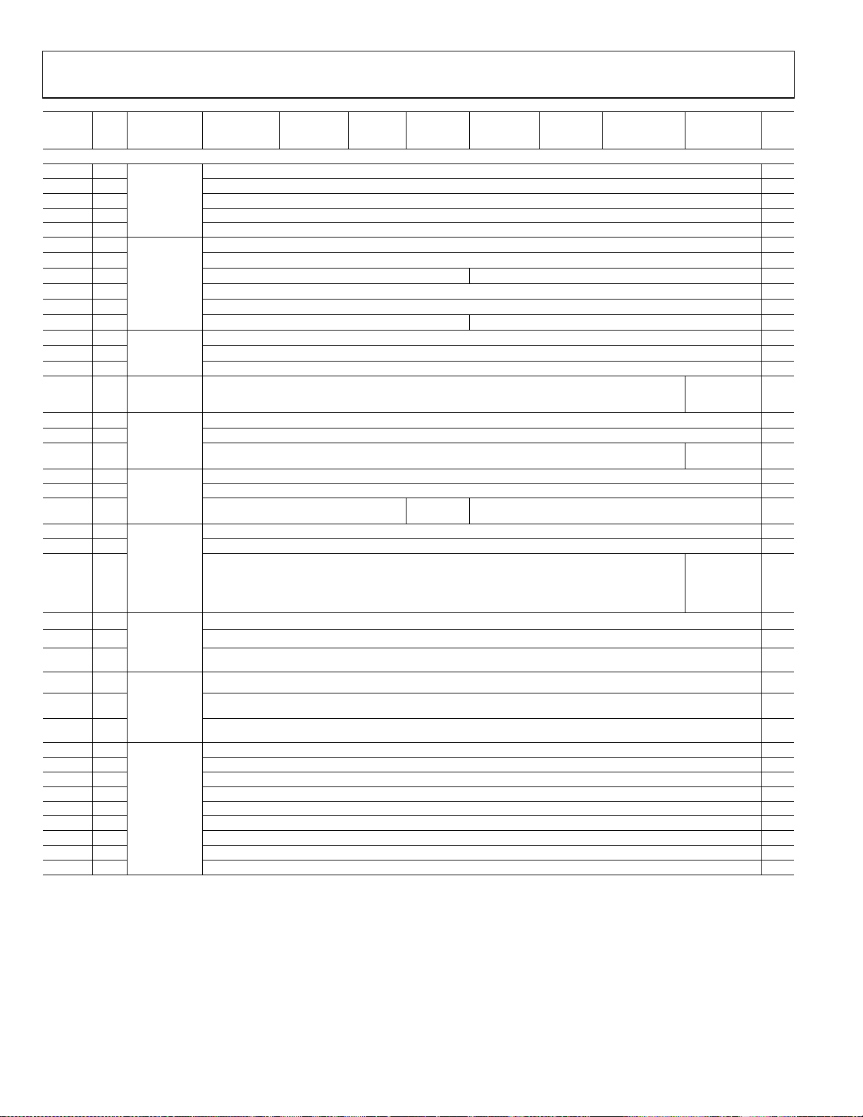
AD9558 Data Sheet
Reg
Addr
(Hex)
Profile B (for REFB)
0x0740 L Reference
0x0741 L Nominal period (fs), Bits[15:8] A2
0x0742 L Nominal period (fs), Bits[23:16] 94
0x0743 L Nominal period (fs), Bits[31:24] 1A
0x0744 L Nominal period (fs), Bits[39:32] 1D
0x0745 L Frequency
0x0746 L
0x0747 L Reserved
0x0748 L
0x0749 L
0x074A L Reserved
0x074B L Validation
0x074C L
0x074D L Reserved 00
0x074E L Select base
0x074F L DPLL loop BW
0x0750 L Digital PLL loop BW scaling factor[15:8] 01
0x0751 L Reserved BW scaling
0x0752 L DPLL
0x0753 L R divider[15:8] 00
0x0754 L Reserved Enable REFB
0x0755 DPLL
0x0756 Digital PLL feedback divider—Integer Part N1[15:8] 5B
0x0757
0x0758 DPLL
0x0759 Digital PLL fractional feedback divider—FRAC1[15:8] 00
0x075A Digital PLL fractional feedback divider—FRAC1[23:16] 00
0x075B DPLL
0x075C Digital PLL feedback divider modulus—MOD1[15:8] 00
0x075D Digital PLL feedback divider modulus—MOD1[23:16] 00
0x075E L Lock detectors Phase lock threshold (ps), Bits[7:0] BC
0x075F L Phase lock threshold(ps), Bits[15:8] 02
0x0760 L Phase lock fill rate[7:0] 0A
0x0761 L Phase lock drain rate[7:0] 0A
0x0762 L Frequency lock threshold[7:0] BC
0x0763 L Frequency lock threshold[15:8] 02
0x0764 L Frequency lock threshold[23:16] 00
0x0765 L Frequency lock fill rate[7:0] 0A
0x0766 L Frequency lock drain rate[7:0] 0A
Opt Name D7 D6 D5 D4 D3 D2 D1 D0 Def
Nominal period (fs), Bits[7:0] (default: 125 μs = 1/(8 kHz) for default system clock setting) 00
Inner tolerance (1 ppm), Bits[7:0] (for reference invalid to valid; 50% down to 1 ppm) (default: 5%)
Inner tolerance (1 ppm), Bits[15:8] (for reference invalid to valid; 50% down to 1 ppm)
Inner tolerance, Bits[19:16]
Outer tolerance (1 ppm), Bits[7:0] (for reference valid to invalid; 50% down to 1 ppm] (default: 10%)
Outer tolerance (1 ppm), Bits[15:8] (for reference valid to invalid; 50% down to 1 ppm)
Outer tolerance, Bits[19:16]
Validation timer (ms), Bits[7:0] (up to 65.5 seconds)
Validation timer (ms), Bits[15:8] (up to 65.5 seconds)
Reserved Sel high PM
base loop
filter
Digital PLL loop BW scaling factor[7:0] (default: 0x01F4 = 50 Hz)
factor[16]
R divider[7:0] 00
divide-by-2
Digital PLL feedback divider—Integer Part N1[7:0] 1F
Reserved Digital PLL
Digital PLL fractional feedback divider—FRAC1[7:0] 00
Digital PLL feedback divider modulus—MOD1[7:0] 01
R divider[19:16] 00
feedback
divider—
Integer Part
N1[16]
14
00
00
0A
00
00
0A
00
00
F4
00
00
period (up to
1.1 ms)
tolerance
loop filter
R divider
(20 bits)
N divider
(17 bits)
fractional
feedback
divider
(24 bits)
fractional
feedback
divider
modulus
(24 bits)
Rev. A | Page 66 of 104
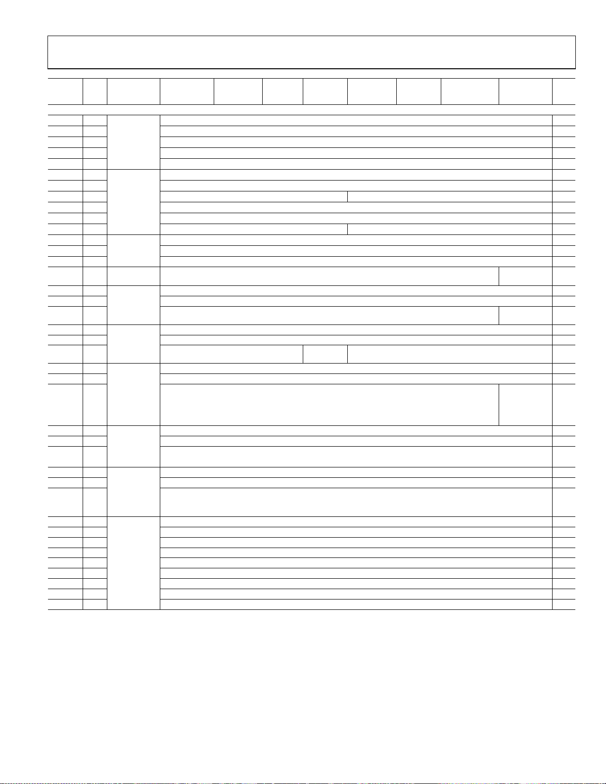
Data Sheet AD9558
Reg
Addr
(Hex)
Profile C (for REFC)
0x0780 L Reference
0x0781 L
0x0782 L
0x0783 L
0x0784 L
0x0785 L Frequency
0x0786 L
0x0787 L Reserved
0x0788 L
0x0789 L
0x078A L Reserved
0x078B L Validation
0x078C L
0x078D L Reserved 00
0x078E L Select base
0x078F L DPLL loop BW Digital PLL loop BW scaling factor[7:0] (default: 0x01F4 = 50 Hz) F4
0x0790 L Digital PLL loop BW scaling factor[15:8] 01
0x0791 L Reserved BW scaling
0x0792 L DPLL
0x0793 L R divider[15:8] 00
0x0794 L Reserved Enable REFC
0x0795 DPLL
0x0796 Digital PLL feedback divider—Integer Part N1[15:8] 07
0x0797 Reserved Digital PLL
0x0798 DPLL
0x0799 Digital PLL fractional feedback divider—FRAC1[15:8] 00
0x079A Digital PLL fractional feedback divider—FRAC1[23:16] 00
0x079B DPLL
0x079C Digital PLL feedback divider modulus—MOD1[15:8] 00
0x079D Digital PLL feedback divider modulus—MOD1[23:16] 00
0x079E L Lock detectors Phase lock threshold (ps), Bits[7:0] BC
0x079F L Phase lock threshold (ps), Bits[15:8] 02
0x07A0 L Phase lock fill rate[7:0] 0A
0x07A1 L Phase lock drain rate[7:0] 0A
0x07A2 L Frequency lock threshold[7:0] BC
0x07A3 L Frequency lock threshold[15:8] 02
0x07A4 L Frequency lock threshold[23:16] 00
0x07A5 L Frequency lock fill rate[7:0] 0A
0x07A6 L Frequency lock drain rate[7:0] 0A
Opt Name D7 D6 D5 D4 D3 D2 D1 D0 Def
period (up to
1.1 ms)
tolerance
loop filter
R divider
(20 bits)
N divider
(17 bits)
fractional
feedback
divider
(24 bits)
fractional
feedback
divider
modulus
(24 bits)
Nominal period (fs), Bits[7:0] (default: 125 μs = 1/(8 kHz) for default system clock setting)
Nominal period (fs), Bits[15:8]
Nominal period (fs), Bits[23:16]
Nominal period (fs), Bits[31:24]
Nominal period (fs), Bits[39:32]
Inner tolerance (1 ppm), Bits[7:0] (for reference invalid to valid; 50% down to 1 ppm) (default: 5%)
Inner tolerance (1 ppm), Bits[15:8] (for reference invalid to valid; 50% down to 1 ppm)
Inner tolerance, Bits[19:16]
Outer tolerance (1 ppm), Bits[7:0] (for reference valid to invalid; 50% down to 1 ppm] (default: 10%)
Outer tolerance (1 ppm), Bits[15:8] (for reference valid to invalid; 50% down to 1 ppm)
Outer tolerance, Bits[19:16]
Validation timer (ms), Bits[7:0] (up to 65.5 seconds)
Validation timer (ms), Bits[15:8] (up to 65.5 seconds)
Reserved
R divider[7:0] C5
divide-by-2
Digital PLL feedback divider—Integer Part N1[7:0] 6B
Digital PLL fractional feedback divider—FRAC1[7:0] 04
Digital PLL feedback divider modulus—MOD1[7:0] 05
R divider[19:16] 00
Sel high PM
base loop filt
factor[16]
feedback
divider—
Integer Part
N1[16]
C9
EA
10
03
00
14
00
00
0A
00
00
0A
00
00
00
00
Rev. A | Page 67 of 104

AD9558 Data Sheet
Reg
Addr
(Hex)
DPLL Profile D (for REFD)
0x07C0 L Reference
0x07C1 L
0x07C2 L
0x07C3 L
0x07C4 L
0x07C5 L Tolerance
0x07C6 L
0x07C7 L Reserved
0x07C8 L
0x07C9 L
0x07CA L Reserved
0x07CB L Validation
0x07CC L
0x07CD L Reserved 00
0x07CE L Select base
0x07CF L DPLL loop BW Digital PLL loop BW scaling factor[7:0] (default: 0x01F4 = 50 Hz) F4
0x07D0 L Digital PLL loop bandwidth BW scaling factor[15:8] 01
0x07D1 L Reserved BW scaling
0x07D2 L DPLL
0x07D3 L R divider[15:8] 00
0x07D4 L Reserved Enable
0x07D5 DPLL
0x07D6 Digital PLL feedback divider—Integer Part N1[15:8] 5B
0x07D7 Reserved Digital PLL
0x07D8 DPLL
0x07D9 Digital PLL fractional feedback divider—FRAC1[15:8] 00
0x07DA Digital PLL fractional feedback divider—FRAC1[23:16] 00
0x07DB DPLL
0x07DC Digital PLL feedback divider modulus—MOD1[15:8] 00
0x07DD Digital PLL feedback divider modulus—MOD1[23:16] 00
0x07DE L Lock detectors Phase lock threshold (ps), Bits[7:0] BC
0x07DF L Phase lock threshold(ps), Bits[15:8] 02
0x07E0 L Phase lock fill rate[7:0] 0A
0x07E1 L Phase lock drain rate[7:0] 0A
0x07E2 L Frequency lock threshold[7:0] BC
0x07E3 L Frequency lock threshold[15:8] 02
0x07E4 L Frequency lock threshold[23:16] 00
0x07E5 L Frequency lock fill rate[7:0] 0A
0x07E6 L Frequency lock drain rate[7:0] 0A
Opt Name D7 D6 D5 D4 D3 D2 D1 D0 Def
period (up to
1.1 ms)
loop filter
Nominal reference period (fs), Bits[7:0] (default: 51.44 ns =1/(19.44 MHz) for default system clock setting)
Nominal period (fs), Bits[15:8]
Nominal period (fs), Bits[23:16]
Nominal period (fs), Bits[31:24]
Nominal period (fs), Bits[39:32]
Inner tolerance (1 ppm), Bits[7:0] (for reference invalid to valid; 50% down to 1 ppm) (default: 5%)
Inner tolerance (1 ppm), Bits[15:8] (for reference invalid to valid; 50% down to 1 ppm)
Inner tolerance, Bits[19:16]
Outer tolerance (1 ppm), Bits[7:0] (for reference valid to invalid; 50% down to 1 ppm) (default: 10%)
Outer tolerance (1 ppm), Bits[15:8] (for reference valid to invalid; 50% down to 1 ppm)
Outer tolerance, Bits[19:16]
Validation timer (ms), Bits[7:0] (up to 65.5 seconds)
Validation timer (ms), Bits[15:8] (up to 65.5 seconds]
Reserved
Sel high PM
base loop
00
A2
94
1A
1D
14
00
00
0A
00
00
0A
00
00
filter
00
00
R divider
(20 bits)
N divider
(17 bits)
fractional
feedback
divider
(24 bits)
fractional
feedback
divider
modulus
(24 bits)
factor[16]
R divider[7:0] 00
REFD
divide-by-2
Digital PLL feedback divider—Integer Part N1[7:0] 1F
Digital PLL fractional feedback divider—FRAC1[7:0] 00
Digital PLL feedback divider modulus—MOD1[7:0] 01
R divider[19:16] 00
feedback
divider—
Integer Part
N1[16]
Rev. A | Page 68 of 104

Data Sheet AD9558
Reg
Addr
(Hex)
Operational Controls
0x0A00 Power-down Soft reset
0x0A01 Loop mode Reserved User
0x0A02 Cal/sync Reserved Soft sync
0x0A03 A Clear/reset
0x0A04 A IRQ clearing Reserved Reserved SYSCLK
0x0A05 A Reserved Pin
0x0A06 A Switching Closed Freerun Holdover Frequency
0x0A07 A Reserved History
0x0A08 A Reserved REFB
0x0A09 A Reserved REFD
0x0A0A A Increment
0x0A0B A Manual
0x0A0C Manual
0x0A0D Static
Quick In-Out Frequency Soft Pin Configuration
0x0C00 L, E Enable
0x0C01 L, E Soft Pin
0x0C02 L, E Reserved SYSCLK PLL REF selection[1:0] 00
0x0C03 L, E Enable
0x0C04 L, E Soft Pin
0x0C05 L, E Channel 3 output frequency
0x0C06 L, E Reserved Sel high
0x0C07 L, A, E Reserved Soft pin start
0x0C08 L, E Reserved Soft pin reset 00
Opt Name D7 D6 D5 D4 D3 D2 D1 D0 Def
functions
phase offset
reference
validation
reference
invalidation
reference
validation
Soft Pin
Section 1
Section 1
Soft Pin
Section 2
Section 2
exclude
regmap
Reserved Clear LF Clear CCI Reserved Clear auto
REFD frequency scale[1:0] REFC frequency
DCO PD SYSCLK
holdover
validated
validated
Output frequency selection[3:0] Input frequency selection[3:0] 00
scale[1:0]
PD
User
freerun
unlocked
REFB fault
cleared
REFD
fault
cleared
Reserved Reset
Reserved Force
Reserved REF Mon
Reserved REF Mon
Ref input
PD
SYSCLK
locked
program
end
updated
REFB fault Reserved REFA
REFD fault Reserved REFC
Reserved En Soft Pin
Reserved En Soft Pin
scale[1:0]
Channel 2 output
frequency scale[1:0]
PM base
loop filter
TDC PD APLL PD Clock dist PD Full PD 00
REF switchover mode[2:0]
sync
APLL
unlocked
Sync clock
dist
unlocked
Frequency
unclamped
Timeout D
Override D
Bypass D
REFB frequency scale[1:0] REFA frequency scale[1:0] 00
Channel 1 output frequency
User ref in manual
00
switchover mode
clock dist
Clear TW
history
APLL
locked
Watchdog
timer
Frequency
locked
Frequency
clamped
validated
validated
phase
offset
Force
Timeout C
REF Mon
Override C
REF Mon
Bypass C
scale[1:0]
DPLL BW[1:0] REF tolerance[1:0] 00
Clear all IRQs Clear watchdog 00
APLL cal ended APLL cal
EEPROM fault EEPROM
Phase
unlocked
Phase slew
unlimited
REFA fault
cleared
REFC fault
cleared
Decrement
phase offset
Force
Timeout B
REF Mon
Override B
REF Mon
Bypass B
Channel 0 output frequency
Reserved 00
started
complete
Phase
locked
Phase slew
limited
REFA fault 00
REFC fault 00
Increment
phase offset
Force
Timeout A
REF Mon
Override A
REF Mon
Bypass A
Section 1
Section 2
scale[1:0]
transfer
00
00
00
00
00
00
00
00
00
00
00
00
Rev. A | Page 69 of 104
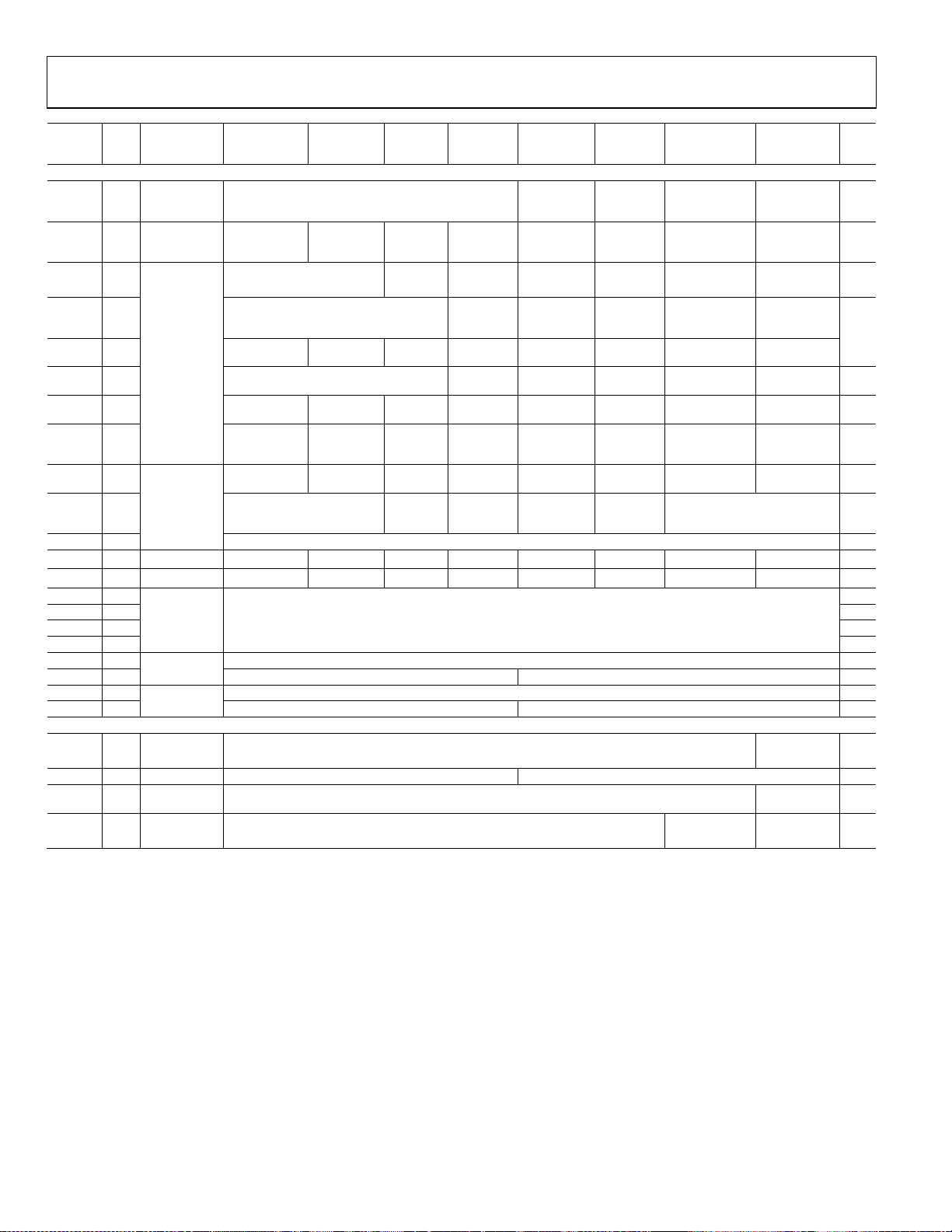
AD9558 Data Sheet
Reg
Addr
(Hex)
Read-Only Status (Accessible During EEPROM Transactions)
0x0D00 R, L EEPROM Reserved Pin program
0x0D01 R, L SYSCLK and
0x0D02 R, L IRQ monitor
0x0D03 R, L Reserved Pin
0x0D04 R, L Switching Closed Freerun Holdover Frequency
0x0D05 R, L Reserved History
0x0D06 R, L Reserved REFB
0x0D07 R, L Reserved REFD
0x0D08 R DPLL Reserved Offset slew
0x0D09 R Reserved Frequency
0x0D0A R Reserved N/A
0x0D0B R REFA/REFB B valid B fault B fast B slow A valid A fault A fast A slow N/A
0x0D0C R REFC/REFD D valid D fault D fast D slow C valid C fault C fast C slow N/A
0x0D0D R Holdover
0x0D0E R N/A
0x0D0F R N/A
0x0D10 R N/A
0x0D11 R Lock detector
0x0D12 R Reserved Phase tub[11:8] N/A
0x0D13 R Lock detector
0x0D14 R Reserved Frequency tub[11:8] N/A
Nonvolatile Memory (EEPROM) Control
0x0E00 E Write protect Reserved Write enable 00
Opt Name D7 D6 D5 D4 D3 D2 D1 D0 Def
PLL status
events
history
phase tub
frequency tub
Reserved DPLL_
APLL_
Lock
Reserved SYSCLK
validated
validated
limiting
All PLLs
locked
unlocked
REFB fault
cleared
REFD
fault
cleared
Frequency
lock
clamped
ROM load
process
APLL VCO
status
SYSCLK
locked
program
end
updated
REFB fault Reserved REFA
REFD
fault
Phase lock Loop
History
available
Tuning word readback[31:0] N/A
APLL cal
in progress
APLL
unlocked
Output dist
sync
unlocked
Frequency
unclamped
Reserved REFC
switching
Reserved Active
Phase tub[7:0] N/A
Frequency tub[7:0] N/A
Fault
detected
APLL lock SYSCLK stable SYSCLK
APLL
lock detect
Watchdog
timer
Frequency
locked
Frequency
clamped
validated
validated
Holdover Active Freerun N/A
reference
priority
Load in
progress
APLL cal ended APLL cal
EEPROM
fault
Phase
unlocked
Phase slew
unlimited
REFA fault
cleared
REFC
fault cleared
Current active reference N/A
Save in
progress
lock detect
started
EEPROM
complete
Phase
locked
Phase slew
limited
REFA fault N/A
REFC
fault
N/A
N/A
N/A
N/A
N/A
N/A
N/A
0x0E01 E Condition Reserved Conditional value[3:0] 00
0x0E02 A,E Save Reserved Save to
0x0E03 A,E Load Reserved Load from
EEPROM
EEPROM
00
00
Rev. A | Page 70 of 104

Data Sheet AD9558
Reg
Addr
(Hex)
EEPROM Storage Sequence
0x0E10 E EEPROM ID Data: two bytes 01
0x0E11 E Address: 0x0006 00
0x0E12 E 06
0x0E13 E System
0x0E14 E Address: 0x0100 01
0x0E15 E 00
0x0E16 E I/O update Action: I/O update 80
0x0E17 E General Data: 18 bytes 11
0x0E18 E Address: 0x0200 02
0x0E19 E 00
0x0E1A E DPLL Data: 47 bytes 2E
0x0E1B E Address: 0x0300 03
0x0E1C E 00
0x0E1D E APLL Data: nine bytes 08
0x0E1E E Address: 0x0400 04
0x0E1F E 00
0x0E20 E Clock dist Data: 22 bytes 15
0x0E21 E Address: 0x0500 05
0x0E22 E 00
0x0E23 E I/O update Action: I/O update 80
0x0E24 E Reference
0x0E25 E Address: 0x0600 06
0x0E26 E 00
0x0E27 E Data: two bytes 01
0x0E28 E Address: 0x0640 06
0x0E29 E 40
0x0E2A E Profile REFA Data: 39 bytes 26
0x0E2B E Address: 0x0700 07
0x0E2C E 00
0x0E2D E Profile REFB Data: 39 bytes 26
0x0E2E E Address: 0x0740 07
0x0E2F E 40
0x0E30 E Profile REFC Data: 39 bytes 26
0x0E31 E Address: 0x0780 07
0x0E32 E 80
0x0E33 E Profile REFD Data: 39 bytes 26
0x0E34 E Address: 0x07C0 07
0x0E35 E C0
0x0E36 E I/O update Action: I/O update 80
0x0E37 E Operational
0x0E38 E Address: 0x0A00 0A
0x0E39 E 00
0x0E3A E Calibrate APLL Action: calibrate output PLL A0
0x0E3B E I/O update Action: I/O update 80
0x0E3C E End of data Action: End of data FF
0x0E3D
to
0xE45
Opt Name D7 D6 D5 D4 D3 D2 D1 D0 Def
clock
inputs
controls
E Unused Unused
(available for additional EEPROM instructions)
Data: nine bytes 08
Data: four bytes 03
Data: 14 bytes 0D
00
Rev. A | Page 71 of 104

AD9558 Data Sheet
REGISTER MAP BIT DESCRIPTIONS
SERIAL PORT CONFIGURATION (REGISTER 0x0000 TO REGISTER 0x0005)
Table 36. Serial Configuration (Note that the contents of Register 0x0000 are not stored to the EEPROM.)
Address Bits Bit Name Description
0x0000 7 SDO enable Enables SPI port SDO pin.
1 = 4-wire (SDO pin enabled).
0 (default) = 3-wire.
6
5 Soft reset
[4:0] Reserved Reserved.
LSB first/increment
address
Table 37. Readback Control
Address Bits Bit Name Description
0x0004 [7:1] Reserved Reserved.
0 Read buffer register
Bit order for SPI port.
1 = least significant bit and byte first.
Register addresses are automatically incremented in multibyte transfers.
0 (default) = most significant bit and byte first.
Register addresses are automatically decremented in multibyte transfers.
Device reset (invokes an EEPROM download or pin program ROM download if EEPROM or
pin program is enabled. See the EEPROM and Pin Configuration and Function Descriptions
sections for details.
For buffered registers, serial port readback reads from actual (active) registers instead of the
buffer.
1 = reads buffered values that take effect on next assertion of I/O update.
0 (default) = reads values currently applied to the device’s internal logic.
Table 38. Soft I/O Update
Address Bits Bit Name Description
[7:1] Reserved Reserved. 0x0005
0 I/O update
Writing a 1 to this bit transfers the data in the serial I/O buffer registers to the device’s
internal control registers. Unless a register is marked as live (as indicated by an L in the Opt
column of the register map), the user must write to this bit before any register settings can
take effect and before a read-only register can be updated with the most current value.
This is an autoclearing bit.
Table 39. User Scratch Pad
Address Bits Bit Name Description
0x0006 [7:0] User scratch pad[7:0]
0x0007 [7:0] User scratch pad[15:8]
User programmable EEPROM ID registers. These registers enable users to write a unique
code of their choosing to keep track of revisions to the EEPROM register loading. It has no
effect on part operation.
0 = default.
SILICON REVISION (REGISTER 0x000A)
Table 40. Silicon Revision
Address Bits Bit Name Description
0x000A [7:0] Silicon revision This read-only register identifies the revision level of the AD9558.
CLOCK PART SERIAL ID (REGISTER 0x000C TO REGISTER 0x000D)
Table 41. Clock Part Family ID
Address Bits Bit Name Description
0x000C [7:0] Clock part family ID[7:0]
0x000D [7:0] Clock part family ID[15:8] This register is a continuation of Register 0x000C.
This read-only register (along with Register 0x000D) uniquely identifies an AD9557 or
AD9558. No other part in the ADI AD95xx family has a value of 0x0001 in these two registers.
Default: 0x01 for the AD9557 and AD9558.
Default: 0x00 for the AD9557 and AD9558.
Rev. A | Page 72 of 104
Data Sheet AD9558
SYSTEM CLOCK (REGISTER 0x0100 TO REGISTER 0x0108)
Table 42. System Clock PLL Feedback Divider (N3 Divider)
Address Bits Bit Name Description
0x0100 [7:0] SYSCLK N3 divider System clock PLL feedback divider value: 4 ≤ N3 ≤ 255 (default: 0x08).
Table 43. SYSCLK Configuration
Address Bits Bit Name Description
0x0101
[7:5] Reserved Reserved.
4
Load from ROM
(reserved)
This reserved bit has no function.
0 (default) = power-on default and ROM not loaded.
1 = ROM values are loaded into the register space.
3 SYSCLK XTAL enable Enables the crystal maintaining amplifier for the system clock input.
1 (default) = crystal mode (crystal maintaining amplifier enabled).
0 = external XO or other system clock source.
[2:1] SYSCLK P divider System clock input divider.
00 (default) = 1.
01 = 2.
10 = 4.
11 = 8.
0 SYSCLK doubler enable Enable clock doubler on system clock input to reduce noise.
0 = disable.
1 (default) = enable.
Table 44. Nominal System Clock Period1
Address Bits Bit Name Description
0x0103 [7:0] System clock period, Bits[7:0].
Nominal system clock period (fs)
Default: 0x0E.
0x0104 [7:0]
System clock period, Bits[15:8].
Default: 0x67.
[7:5] Reserved Reserved. 0x0105
[4:0] Nominal system clock period (fs)
1
Note that the default setting for system clock period is 1.271566 ns, which is the period of 786.432 MHz (= 49.152 MHz × 16).
System clock period, Bits[20:16].
Default: 0x13.
Table 45. System Clock Stability Period
Address Bits Bit Name Description
0x0106 [7:0]
System clock stability period (ms)
System clock period, Bits[7:0].
Default: 0x32 (0x000032 = 50 ms).
0x0107 [7:0]
System clock period, Bits[15:8].
Default: 0x00.
0x0108
[7:5] Reserved Reserved.
4 Reset SYSCLK stability timer This autoclearing bit resets the system clock stability timer.
[3:0] System clock stability period
System clock period, Bits[19:16].
Default: 0x00.
Rev. A | Page 73 of 104

AD9558 Data Sheet
GENERAL CONFIGURATION (REGISTER 0x0200 TO REGISTER 0x0214)
Multifunction Pin Control (M0 to M7) and IRQ Pin Control (Register 0x0200 to Register 0x0209)
Note that the default setting for the M0 to M5 multifunction pins and the IRQ is that of a 3-level logic input; M6 and M7 are unused inputs at
startup. After startup, M0 to M7 are 2-level inputs or 2-level outputs, based on the settings of Register 0x0200 to Register 0x0208. Setting
Bit 0 in Register 0x0200 to 1 enables M0 to M7 pin functionality.
Table 46. Multifunction Pin (M0 to M7) Control
Address Bits Bit Name Description
[7:1] Reserved Reserved. 0x0200
0
0x0201
0x0202
0x0203
0x0204
0x0205
0x0206
0x0207
0x0208
Enable M pins and IRQ pin
function
7
M0 output/input
[6:0] M0 function See Table 129 and Table 130. Default: 0xB0 = REFA valid.
7
M1 output/input
[6:0] M1 function See Table 129 and Table 130. Default: 0xB1 = REFB valid.
7
M2 output/input
[6:0] M2 function See Table 129 and Table 130. Default: 0xC0 = REFA active.
7
M3 output/input
[6:0] M3 function See Table 129 and Table 130. Default: 0xC1 = REFB active.
7
M4 output/input
[6:0] M4 function See Table 129 and Table 130. Default: 0xB2 = REFC valid.
7
M5 output/input
[6:0] M5 function See Table 129 and Table 130. Default: 0xB3 = REFD valid.
7
M6 output/input
[6:0] M6 function See Table 129 and Table 130. Default: 0xC2 = REFC active.
7
M7 output/input
[6:0] M7 function See Table 129 and Table 130. Default: 0xC3 = REFD active.
0 (default) = disables the function of the M pins and IRQ pin control register (Address
0x0201 to Address 0x0209) and the M pins and IRQ pin are in 3-level logic input state.
1 = the M pins and IRQ pin are out of 3-level logic input state. Enables the function of the
M pins and IRQ pin control register (Address 0x0201 to Address 0x0209).
In/out control for M0 pin.
0 = input (2-level logic control pin).
1 (default) = output (2-level logic status pin).
In/out control for M1 pin (same as M0).
In/out control for M2 pin (same as M0).
In/out control for M3 pin (same as M0).
In/out control for M3 pin (same as M0).
In/out control for M3 pin (same as M0).
In/out control for M3 pin (same as M0).
In/out control for M3 pin (same as M0).
Table 47. IRQ Pin Output Mode
Address Bits Bit Name Description
0x0209
[7:5] Reserved Default: 000b
[4:3] Status signal at IRQ pin This selection is valid only when Address 0x0209[2] = 1
00 = DPLL phase locked
01 = DPLL frequency locked
10 = system clock PLL locked
11 (default) = (DPLL phase locked) AND (system clock PLL locked) AND (APLL locked)
2 Use IRQ pin for status signal 0 = uses IRQ pin to monitor IRQ event
1 (default) = uses IRQ pin to monitor internal status signals
[1:0] IRQ pin driver type Select the output mode of the IRQ pin
00 = NMOS, open drain (requires an external pull-up resistor)
01 = PMOS, open drain (requires an external pull-down resistor)
10 = CMOS, active high
11 (default) = CMOS, active low
Rev. A | Page 74 of 104
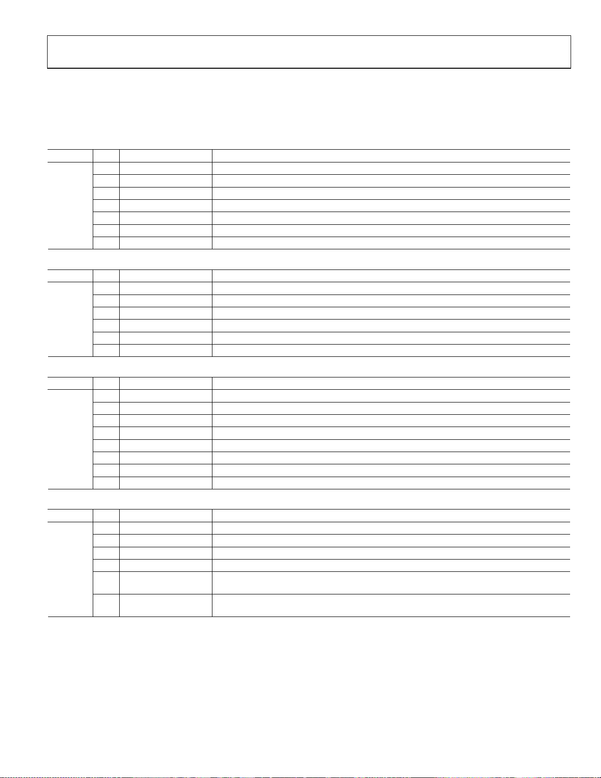
Data Sheet AD9558
IRQ MASK (REGISTER 0x020A TO REGISTER 0x020F)
The IRQ mask register bits form a one-to-one correspondence with the bits of the IRQ monitor register (0x0D02 to 0x0D09). When set to
Logic 1, the IRQ mask bits enable the corresponding IRQ monitor bits to indicate an IRQ event. The default for all IRQ mask bits is Logic 0,
which prevents the IRQ monitor from detecting any internal interrupts.
Table 48. IRQ Mask for SYSCLK
Address Bits Bit Name Description
0x020A
Table 49. IRQ Mask for Distribution Sync, Watchdog Timer, and EEPROM
Address Bits Bit Name Description
0x020B
[7:6] Reserved Reserved
5 SYSCLK unlocked Enables IRQ for indicating a SYSCLK PLL state transition from locked to unlocked
4 SYSCLK locked Enables IRQ for indicating a SYSCLK PLL state transition from unlocked to locked
3 APLL unlocked Enables IRQ for indicating an APLL state transition from locked to unlocked
2 APLL locked Enables IRQ for indicating an APLL state transition from unlocked to locked
1 APLL cal complete Enables IRQ for indicating that APLL (LCVCO) calibration has completed
0 APLL cal started Enables IRQ for indicating that APLL (LCVCO) calibration has begun
[7:5] Reserved Reserved
4 Pin program end Enables IRQ for indicating successful completion of a pin program ROM load
3 Sync distribution Enables IRQ for indicating a distribution sync event
2 Watchdog timer Enables IRQ for indicating expiration of the watchdog timer
1 EEPROM fault Enables IRQ for indicating a fault during an EEPROM load or save operation
0 EEPROM complete Enables IRQ for indicating successful completion of an EEPROM load or save operation
Table 50. IRQ Mask for the Digital PLL
Address Bits Bit Name Description
0x020C
7 Switching Enables IRQ for indicating that the DPLL is switching to a new reference
6 Closed Enables IRQ for indicating that the DPLL has entered closed-loop operation
5 Freerun Enables IRQ for indicating that the DPLL has entered free run mode
4 Holdover Enables IRQ for indicating that the DPLL has entered holdover mode
3 Frequency unlocked Enables IRQ for indicating that the DPLL lost frequency lock
2 Frequency locked Enables IRQ for indicating that the DPLL has acquired frequency lock
1 Phase unlocked Enables IRQ for indicating that the DPLL lost phase lock
0 Phase locked Enables IRQ for indicating that the DPLL has acquired phase lock
Table 51. IRQ Mask for History Update, Frequency Limit and Phase Slew Limit
Address Bits Bit Name Description
0x020D
[7:5] Reserved Reserved
4 History updated Enables IRQ for indicating the occurrence of a tuning word history update
3 Frequency unclamped Enables IRQ for indicating a frequency limit state transition from clamped to unclamped
2 Frequency clamped Enables IRQ for indicating a state transition of the frequency limiter from unclamped to clamped
1 Phase slew unlimited
0 Phase slew limited
Enables IRQ for indicating a state transition of the phase slew limiter from slew limiting to not
slew limiting
Enables IRQ for indicating a state transition of the phase slew limiter from not slew limiting to
slew limiting
Rev. A | Page 75 of 104

AD9558 Data Sheet
Table 52. IRQ Mask for Reference Inputs
Address Bits Bit Name Description
0x020E
0x020F
Table 53. Watchdog Timer 11
Address Bits Bit Name Description
0x0210 [7:0] Watchdog timer, Bits[7:0]; default: 0x00
0x0211 [7:0]
1
Note that the watchdog timer is expressed in units of milliseconds (ms). The default value is 0 (disabled).
DPLL CONFIGURATION (REGISTER 0x0300 TO REGISTER 0x032E)
Table 54. Free Run Frequency Tuning Word1
Address Bits Bit Name Description
0x0300 [7:0] Free run frequency tuning word, Bits[7:0]; default: 0x11
0x0301 [7:0] Free run frequency tuning word, Bits[15:8]; default: 0x15
0x0302 [7:0]
0x0303 [7:6] Reserved
[5:0] 30-bit free run frequency word Free run frequency tuning word, Bits[29:24]; default: 0x1B
1
Note that the default free run tuning word is 0x1B641511, which is used for 8 kHz/19.44 MHz = 622.08 MHz translation.
7 Reserved Reserved
6 REFB validated Enables IRQ for indicating that REFB has been validated
5 REFB fault cleared Enables IRQ for indicating that REFB has been cleared of a previous fault
4 REFB fault Enables IRQ for indicating that REFB has been faulted
3 Reserved Reserved
2 REFA validated Enables IRQ for indicating that REFA has been validated
1 REFA fault cleared Enables IRQ for indicating that REFA has been cleared of a previous fault
0 REFA fault Enables IRQ for indicating that REFA has been faulted
[7:0] Reserved Reserved
Watchdog timer (ms)
Watchdog timer, Bits[15:8]; default: 0x00
30-bit free run frequency tuning word
Free run frequency tuning word, Bits[23:9]; default: 0x64
Reserved
Table 55. Digital Oscillator Control
Address Bits Bit Name Description
0x0304
[7:6] Reserved Default: 00b
5 DCO 4-level output 0 (default) = DCO 3-level output mode
1 = enables DCO 4-level output mode
4 Reserved Reserved (must be set to 1b)
[3:0] Reserved Reserved (default: 0x0)
Table 56. DPLL Frequency Clamp
Address Bits Bit Name Description
0x0306 [7:0]
0x0307 [7:0]
Lower limit of pull-in range (expressed
as a 20-bit frequency tuning word)
Lower limit pull-in range, Bits[7:0].
Default: 0x51.
Lower limit pull-in range, Bits[15:8].
Default: 0xB8.
0x0308 [7:4]
[3:0]
Reserved
Lower limit of pull-in range
Default: 0x0.
Lower limit pull-in range, Bits[19:16].
Default: 0x2.
0x0309 [7:0]
0x030A [7:0]
Upper limit of pull-in range
(expressed as a 20-bit frequency
tuning word)
Upper limit pull-in range, Bits[7:0].
Default: 0x3E.
Upper limit pull-in range, Bits[15:8].
Default: 0x0A.
0x030B [7:4]
[3:0] Upper limit of pull-in range
Reserved
Default: 0x0.
Upper limit pull-in range, Bits[19:16].
Default: 0xB.
Rev. A | Page 76 of 104

Data Sheet AD9558
Table 57. Fixed Closed-Loop Phase Lock Offset
Address Bits Bit Name Description
0x030C [7:0]
0x030D [7:0]
0x030E [7:0]
0x030F [7:6] Reserved Reserved; default: 0x0.
Table 58. Incremental Closed-Loop Phase Lock Offset Step Size1
Address Bits Bit Name Description
0x0310 [7:0]
0x0311 [7:0]
1
Note that the default incremental closed-loop phase lock offset step size value is 0x0000 = 0 (0 ns).
Table 59. Phase Slew Rate Limit
Address Bits Bit Name Description
0x0312 [7:0]
0x0313 [7:0]
Fixed phase lock offset (signed; ps)
[5:0] Fixed phase lock offset (signed; ps)
Incremental phase lock offset
step size (ps)
Phase slew rate limit (µs/sec)
Fixed phase lock offset, Bits[7:0].
Default: 0x00.
Fixed phase lock offset, Bits[15:8].
Default 0x00.
Fixed phase lock offset, Bits[23:16].
Default: 0x00.
Fixed phase lock offset, Bits[29:24].
Default: 0x00.
Incremental phase lock offset step size, Bits[7:0].
Default: 0x00.
This controls the static phase offset of the DPLL while it is locked.
Incremental phase lock offset step size, Bits[15:8].
Default: 0x00.
This controls the static phase offset of the DPLL while it is locked.
Phase slew rate limit, Bits[7:0].
Default: 0x00.
This register controls the maximum allowable phase slewing during transients
and reference switching.
The default phase slew rate limit is 0, or disabled. Minimum useful value is 310 µs/sec.
Phase slew rate limit, Bits[15:8].
Default: 0x00.
Table 60. History Accumulation Timer
Address Bits Bit Name Description
0x0314 [7:0]
History accumulation timer (ms)
History accumulation timer bits[7:0].
Default: 0x0A. For Register 0x0314 and Register 0x0315, 0x000A = 10 ms.
Maximum is 65 sec. This register controls the amount of tuning word averaging used
to determine the tuning word used in holdover. Never program a timer value of
zero. The default value is 0x000A = 10 decimal, which equates to 10 ms
0x0315 [7:0]
History accumulation timer bits[15:8].
Default: 0x00.
Rev. A | Page 77 of 104

AD9558 Data Sheet
Table 61. History Mode
Address Bits Bit Name Description
0x0316 [7:5] Reserved Reserved.
4 Single sample fallback
3 Persistent history Controls holdover history initialization. When switching to a new reference:
[2:0] Incremental average History mode value from 0 to 7 (default: 0).
Table 62. Base Digital Loop Filter with High Phase Margin (PM = 88.5°, BW = 0.1 Hz, Third Pole Frequency = 10 Hz, N1 = 1)1
Address Bits Bit Name Description
0x0317 [7:0] HPM Alpha-0 linear Alpha-0 coefficient linear bits[7:0]. Default: 0x8C
0x0318 [7:0] Alpha-0 coefficient linear bits[15:8]
0x0319 7 Reserved Reserved
[6:0] HPM Alpha-1 exponent Alpha-1 coefficient exponent bits[6:0]
0x031A [7:0] HPM Beta-0 linear Beta-0 coefficient linear bits[7:0]
0x031B [7:0] Beta-0 coefficient linear bits[15:8]
0x031C 7 Reserved Reserved
[6:0] HPM Beta-1 exponent Beta-1 coefficient exponent bits[6:0]
0x031D [7:0] HPM Gamma-0 linear Gamma-0 coefficient linear bits[7:0]
0x031E [7:0] Gamma-0 coefficient linear bits[15:8]
0x031F 7 Reserved Reserved
[6:0] HPM Gamma-1 exponent Gamma-1 coefficient exponent bits[6:0]
0x0320 [7:0] HPM Delta-0 linear Delta-0 coefficient linear bits[7:0]
0x0321 [7:0] Delta-0 coefficient linear bits[15:8]
0x0322 7 Reserved Reserved
[6:0] HPM Delta-1 exponent Delta-1 coefficient exponent bits[6:0]
1
Note that the base digital loop filter coefficients (α, β, γ, and δ) have the following general form: x(2y), where x is the linear component and y is the exponential
component of the coefficient. The value of the linear component (x) constitutes a fraction, where 0 ≤ x ≤ 1. The exponential component (y) is a signed integer.
Controls holdover history. If tuning word history is not available for the reference
that was active just prior to holdover, then:
0 (default) = uses the free run frequency tuning word register value.
1 = uses the last tuning word from the DPLL.
0 (default) = clears the tuning word history.
1 = retain the previous tuning word history.
When set to non-zero, causes the first history accumulation to update prior to the
first complete averaging period. After the first full interval, updates occur only at the
full period.
0 (default) = update only after the full interval has elapsed.
1 = update at 1/2 the full interval.
2 = update at 1/4 and 1/2 of the full interval.
3 = update at 1/8, 1/4, and 1/2 of the full interval.
...
7 = update at 1/256, 1/128, 1/64, 1/32, 1/16, 1/8, 1/4, and 1/2 of the full interval.
Rev. A | Page 78 of 104

Data Sheet AD9558
Table 63. Base Digital Loop Filter with Normal Phase Margin (PM = 70°, BW = 0.1 Hz, Third Pole Frequency = 2 Hz, N1 = 1)1
Address Bits Bit Name Description
0x0323 [7:0] Alpha-0 coefficient linear, Bits[7:0]
0x0324 [7:0]
0x0326 [7:0] NPM Beta-0 linear Beta-0 coefficient linear, Bits[7:0]
0x0327 [7:0] Beta-0 coefficient linear, Bits[15:8]
0x0328 7 Reserved Reserved
[6:0] NPM Beta-1 exponent Beta-1 coefficient exponent, Bits[6:0]
0x0329 [7:0] NPM Gamma-0 linear Gamma-0 coefficient linear, Bits[7:0]
0x032A [7:0] Gamma-0 coefficient linear, Bits[15:8]
0x032B 7 Reserved Reserved
[6:0] NPM Gamma-1 exponent Gamma-1 coefficient exponent, Bits[6:0]
0x032C [7:0] NPM Delta-0 linear Delta-0 coefficient linear, Bits[7:0]
0x032D [7:0] Delta-0 coefficient linear, Bits[15:8]
0x032E 7 Reserved Reserved
[6:0] NPM Delta-1 exponent Delta-1 coefficient exponent, Bits[6:0]
1
Note that the digital loop filter base coefficients (α, β, γ, and δ) have the following general form: x(2y), where x is the linear component and y is the exponential
component of the coefficient. The value of the linear component (x) constitutes a fraction, where 0 ≤ x ≤ 1. The exponential component (y) is a signed integer.
NPM Alpha-0 linear
Alpha-0 coefficient linear, Bits[15:8]
7 Reserved Reserved 0x0325
[6:0] NPM Alpha-1 exponent Alpha-1 coefficient exponent, Bits[6:0]
OUTPUT PLL CONFIGURATION (REGISTER 0x0400 TO REGISTER 0x0408)
Table 64. Output PLL Setting1
Address Bits Bit Name Description
0x0400 [7:0]
0x0401 [7:0] APLL N divider Division = 14 to 255
0x0402 [7:0] Reserved Reserved; default: 0x00
0x0403 [7:6] APLL loop filter control Pole 2 resistor Rp2; default: 0x07
500 (default) 0 0
333 0 1
250 1 0
200 1 1
[5:3]
Output PLL (APLL)
charge pump current
LSB = 3.5 µA
00000001b = 1 × LSB; 00000010b = 2 × LSB; 11111111b = 255 × LSB
Default: 0x81 = 451 µA CP current
Default: 0x14 = divide-by-20
Rp2 (Ω) Bit 7 Bit 6
Zero resistor, Rzero
Rzero (Ω) Bit 5 Bit 4 Bit 3
1500 (default) 0 0 0
1250 0 0 1
1000 0 1 0
930 0 1 1
1250 1 0 0
1000 1 0 1
750 1 1 0
680 1 1 1
Rev. A | Page 79 of 104

AD9558 Data Sheet
Address Bits Bit Name Description
[2:0]
[7:1] Reserved Default: 0x00. 0x0404
0 Bypass internal Rzero
0x0405
[7:4] Reserved Default: 0x2.
3
APLL locked controlled
sync
[2:1] Reserved Default: 00b.
0
Manual APLL
1
Note that the default APLL loop BW is 180 KHz.
VCO calibration
Pole 1 Cp1.
Cp1 (pF) Bit 2 Bit 1 Bit 0
0
20
80
100
20
40
100
120 (default)
0
0
0
0
1
1
1
1
0
0
1
1
0
0
1
1
0
1
0
1
0
1
0
1
0 (default) = uses the internal Rzero resistor.
1 = bypasses the internal Rzero resistor (makes Rzero = 0 and requires the use of a series
external zero resistor).
0 (default) = the clock distribution sync function is not enabled until the output PLL (APLL) is
calibrated and locked. After APLL calibration and lock, the output clock distribution sync is
armed, and the sync function for the clock outputs is under the control of Register 0x0500.
1 = overrides the lock detector state of the output PLL; allows Register 0x0500 to control
the output sync function, regardless of the APLL lock status.
1 = initiates VCO calibration. (Calibration occurs on low-to-high transition.)
0 (default) = does nothing. This is not an autoclearing bit.
Table 65. Reserved
Address Bits Bit Name Description
0x0406 [7:0] Reserved Default: 0x00
Table 66. RF Divider Setting
Address Bits Bit Name Description
0x0407
[7:4] RF Divider 2 division
0000/0001 = 3
0010 = 4
0011 = 5
0100 = 6 (default)
0101 = 7
0110 = 8
0111 = 9
1000 = 10
1001 = 11
[3:0] RF Divider 1 division
0000/0001 = 3
0010 = 4
0011 = 5
0100 = 6 (default)
0101 = 7
0110 = 8
0111 = 9
1000 = 10
1001 = 11
0x0408
[7:5] Reserved Reserved. Default: 000b
4 RF divider start-up mode
0 (default) = RF dividers are held in power-down until the APLL feedback divider is
detected, which ensures proper RF divider operation when exiting full power-down
1 = RF dividers are not held in power-down until the APLL feedback divider is detected
[3:2] Reserved Reserved. Default: 00b
1 PD RF Divider 2
0 = enables RF Divider 2
1 (default) = powers down RF Divider 2
0 PD RF Divider 1 0 (default) = enables RF Divider 1
1 = powers down RF Divider 1
Rev. A | Page 80 of 104

Data Sheet AD9558
OUTPUT CLOCK DISTRIBUTION (REGISTER 0x0500 TO REGISTER 0x0515)
Table 67. Clock Distribution Output Synchronization Settings
Address Bits Bit Name Description
0x0500
7 Mask Channel 3 sync Masks the synchronous reset to the Channel 3 (M3) divider.
0 (default) = unmasked. The output drivers do not toggle until a SYNC pulse occurs.
1 = masked. Setting this bit asynchronously releases Channel 3 from the static SYNC state,
thus allowing the Channel 3 divider to toggle. Channel 3 ignores all SYNC events while
this bit is set. Setting this bit does not enable the output drivers connected to this channel. In
addition, the output distribution sync also depends on the setting of Register 0x0405[3].
6 Mask Channel 2 sync Masks the synchronous reset to the Channel 2 (M2) divider.
0 (default) = unmasked. The output drivers do not toggle until a SYNC pulse occurs.
1 = masked. Setting this bit asynchronously releases Channel 2 from the static SYNC state,
thus allowing the Channel 2 divider to toggle. Channel 2 ignores all SYNC events while
this bit is set. Setting this bit does not enable the output drivers connected to this channel. In
addition, the output distribution sync also depends on the setting of Register 0x0405[3].
5 Mask Channel 1 sync Masks the synchronous reset to the Channel 1 (M2) divider.
0 (default) = unmasked. The output drivers do not toggle until a SYNC pulse occurs.
1 = masked. Setting this bit asynchronously releases Channel 1 from the static SYNC state,
thus allowing the Channel 1 divider to toggle. Channel 1 ignores all SYNC events while
this bit is set. Setting this bit does not enable the output drivers connected to this
channel. In addition, the output distribution sync also depends on the setting of Register
0x0405[3].
4 Mask Channel 0 sync Masks the synchronous reset to the Channel 0 (M0) divider.
0 (default) = unmasked. The output drivers do not toggle until a SYNC pulse occurs.
1 = masked. Setting this bit asynchronously releases Channel 0 from the static SYNC state,
thus allowing the Channel 0 divider to toggle. Channel 0 ignores all SYNC events while
this bit is set. Setting this bit does not enable the output drivers connected to this channel. In
addition, the output distribution sync also depends on the setting of Register 0x0405[3].
3 Reserved Default: 0b.
2 Sync source selection Selects the sync source for the clock distribution output channels.
0 (default) = direct. The sync pulse happens on the next I/O update.
1 = active reference.
Note that the output distribution sync also depends on the APLL being calibrated and
locked unless Register 0x0405[3] = 1b.
[1:0] Automatic sync mode Autosync mode.
00 = disabled. A sync command must be issued manually, or by using the mask sync bits
in this register (Bits[7:4]).
01 = sync on DPLL frequency lock.
10 (default) = sync on DPLL phase lock.
11 = reserved.
Rev. A | Page 81 of 104

AD9558 Data Sheet
Table 68. Distribution OUT0 Setting
Address Bits Bit Name Description
0x0501 7 Enable 3.3 V CMOS driver 0 (default) = disables 3.3 V CMOS driver; the OUT5 1.8 V logic is controlled by Register 0x0501[6:4].
1 = enables 3.3 V CMOS driver as operating mode of OUT0.
This bit should be enabled only if Bits[6:4] are in CMOS mode.
[6:4] OUT0 format
[3:2] OUT0 polarity Control the OUT0 polarity.
1 OUT0 drive strength Controls the output drive capability of OUT0.
0 Enable OUT0
This control is valid when Register 0x0501[7] = 0.
When Register 0x0501[7] = 1, OUT5 is in 3.3 V CMOS mode and these bits are ignored.
Select the operating mode of OUT0.
000 = PD, tristate.
001 (default) = HSTL.
010 = LVDS.
011 = reserved.
100 = CMOS, both outputs active.
101 = CMOS, P output active, N output power-down.
110 = CMOS, N output active, P output power-down.
111 = reserved.
00 (default) = positive, negative.
01 = positive, positive.
10 = negative, positive.
11 = negative, nevative.
0 (default) = CMOS: low drive strength; LVDS: 3.5 mA nominal.
1 = CMOS: normal drive strength; LVDS: 4.5 mA nominal (LVDS boost mode).
Note that this is only in 3.3 V CMOS mode for CMOS strength.
1.8 V CMOS has only the low drive strength.
Enables/disables (1b/0b) OUT0 1.8 V driver (default is disabled).
This bit does not enable/disable OUT0 if Bit 7 of this register is set.
Table 69. Distribution Channel 0 Divider Setting
Address Bits Bit Name Description
0x0502 [7:0]
0x0503 [7:4] Reserved Reserved.
3 Channel 0 PD 0 (default) = normal operation.
2 Select RF Divider 2 1 = selects RF Divider 2 as prescaler for Channel 0 divider.
[1:0]
Channel 0 (M0)
division ratio
Channel 0 (M0)
division ratio
[7:6] Reserved Reserved. Default: 00b 0x0504
[5:0] Channel 0 divider phase
10-bit channel divider bits[7:0] (LSB).
Division equals channel divider, Bits[9:0] + 1.
(Bits[9:0] = 0 is divide-by-1, Bits[9:0] = 1 is divide-by-2…Bits[9:0] = 1023 is divide-by-1024)
1 = powers down Channel 0.
0 (default) = selects RF Divider 1 as prescaler for Channel 0 divider.
10-bit channel divider, Bits[9:8] (MSB)
Divider initial phase after sync relative to the divider input clock (from the RF divider
output). LSB is ½ of a period of the divider input clock. Default: 00000b.
Phase = 0 is no phase offset.
Phase = 1 is ½ a period offset.
Rev. A | Page 82 of 104

Data Sheet AD9558
Table 70. Distribution OUT1 Setting
Address Bits Bit Name Description
0x0505
0x0506
7 Reserved Reserved; default: 0b
[6:4] OUT1 format
[3:2] OUT1 polarity
1 OUT1 drive strength
0 Enable OUT1 Setting this bit enables the OUT1 driver (default is disabled)
7 Reserved Reserved; default: 0b
[6:4] OUT2 format
[3:2] OUT2 polarity
1 OUT2 drive strength
0 Enable OUT2 Setting this bit enables the OUT2 driver (default is disabled)
Select the operating mode of OUT1
000 = PD, tristate
001 (default) = HSTL
010 = LVDS
011 = reserved
100 = CMOS, both outputs active
101 = CMOS, P output active, N output power-down
110 = CMOS, N output active, P output power-down
111 = reserved
Configure the OUT1 polarity in CMOS mode and are active in CMOS mode only
00 (default) = positive, negative
01 = positive, positive
10 = negative, positive
11 = negative, negative
Controls the output drive capability of OUT1
0 (default) = LVDS: 3.5 mA nominal
1 = LVDS: 4.5 mA nominal (LVDS boost mode)
No CMOS control because OUT1 is 1.8 V CMOS only
Select the operating mode of OUT2
000 = PD, tristate
001 (default) = HSTL
010 = LVDS
011 = reserved
100 = CMOS, both outputs active
101 = CMOS, P output active, N output power-down
110 = CMOS, N output active, P output power-down
111 = reserved
Configure the OUT2 polarity in CMOS mode and are active in CMOS mode only
00 (default) = positive, negative
01 = positive, positive
10 = negative, positive
11 = negative, negative
Controls the output drive capability of OUT2
0 (default) = LVDS: 3.5 mA nominal
1 = LVDS: 4.5 mA nominal (LVDS boost mode)
No CMOS control because OUT2 is 1.8 V CMOS only
Table 71. Distribution Channel 1 Divider Setting
Address Bits Bit Name Description
0x0507 [7:0] Channel 1 divider The same control for Channel 1 divider as in Register 0x0502 for Channel 0 divider
0x0508 [7:0] Channel 1 divider The same control for Channel 1 divider as in Register 0x0503 for Channel 0 divider
0x0509 [7:0] Channel 1 divider The same control for Channel 1 divider as in Register 0x0504 for Channel 0 divider
Table 72. Clock Distribution Channel 2 and OUT3, OUT4 Driver Settings
Address Bits Bit Name Description
0x050A [7:0] OUT3 The same control for OUT3 as in Register 0x0505 for OUT1
0x050B [7:0] OUT4 The same control for OUT4 as in Register 0x0505 for OUT1
0x050C [7:0] Channel 2 divider The same control for Channel 2 divider as in Register 0x0502 for Channel 0 divider
0x050D [7:0] Channel 2 divider The same control for Channel 2 divider as in Register 0x0503 for Channel 0 divider
0x050E [7:0] Channel 2 divider The same control for Channel 2 divider as in Register 0x0504 for Channel 0 divider
Rev. A | Page 83 of 104

AD9558 Data Sheet
Table 73. Clock Distribution Channel 3 and OUT5 Driver Settings
Address Bits Bit Name Description
0x050F
0x0510 [7:0]
0x0512 [7:0]
0x0513
0x0514 [7:0]
0x0515 [7:0]
7 Enable 3.3 V CMOS driver 0 (default) = disable 3.3 V CMOS driver; the OUT5 1.8 V logic is controlled by Register 0x050F[6:4].
1 = enable 3.3 V CMOS driver as operating mode of OUT5.
This bit should be enabled only if Bits[6:4] are in CMOS mode.
[6:4] OUT5 format
[3:2] OUT5 polarity Control the OUT5 polarity.
1 OUT5 drive strength Controls the output drive capability of OUT5.
0 OUT5 enable
Channel 3, Divider 1 (M3)
division ratio
[7:2] Reserved Reserved. 0x0511
[1:0]
Channel 3, Divider 1 (M3)
division ratio
Channel 3, Divider 2
(M3b) division ratio
[7:4] Reserved Reserved.
4 Channel 3 doubler 0 (default) = normal operation.
3 PD Channel 3 0 (default) = normal operation.
2
Select RF divider
for Channel 2
[1:0]
Channel 3, Divider 2
(M3b) division ratio
Channel 3, Divider 1 (M3)
phase
Channel 3, Divider 2
(M3b) phase
This control is valid when Register 0x050F[7] = 0; when Register 0x050F[7] = 1, OUT5 is in 3.3 V
CMOS mode and these bits are ignored.
Select the operating mode of OUT5.
000 = PD, tristate.
001 (default) = HSTL.
010 = LVDS.
011 = reserved.
100 = CMOS, both outputs active.
101 = CMOS, P output active, N output power-down.
110 = CMOS, N output active, P output power-down.
111 = reserved.
00 (default) = positive, negative.
01 = positive, positive.
10 = negative, positive.
11 = negative, negative.
0 (default) = CMOS: low drive strength, LVDS: 3.5 mA nominal.
1 = CMOS: normal drive strength, LVDS: 4.5 mA nominal (LVDS boost mode).
Note that this is only in 3.3 V CMOS mode for CMOS strength.
1.8 V CMOS has only the low drive strength.
Enables/disables (1b/0b) OUT5 1.8 V driver (default is disabled).
This bit does not enable/disable OUT5 if Bit 7 of this register is set.
10-bit channel divider, Bits[7:0] (LSB) (default: 0x03).
Division equals channel divider, Bits[9:0] + 1.
(Bits[9:0] = 0 is divide-by-1, Bits[9:0] = 1 is divide-by-2…Bits[9:0] = 1023 is divide-by-1024).
10-bit channel divider, Bits[9:8] (MSB) (default: 0x00).
10-bit channel divider, Bits[7:0] (LSB).
Division equals channel divider bits[9:0] + 1 .
(Bits[9:0] = 0 is divide-by-1, Bits[9:0] = 1 is divide-by-2…Bits[9:0] = 1023 is divide-by-1024).
1 = enables Channel 3 clock doubler. This bit activates an internal clock doubler that doubles
the frequency of the Channel 3 divider. In this mode, Channel 3, Divider 2 is bypassed.
1 = powers down Channel 3.
1 = selects RF Divider 2 as prescaler for the Channel 3 divider.
0 (default) = selects RF Divider 1 as a prescaler for the Channel 3 divider.
10-bit channel divider, Bits[9:8] (MSB).
The same control for Channel 3, Divider 1 phase as found in Register 0x0504 for Channel 0
divider phase (default: 0x00).
The same control for Channel 3, Divider 2 phase as found in Register 0x0504 for Channel 0
divider phase (default: 0x00).
Rev. A | Page 84 of 104
Data Sheet AD9558
REFERENCE INPUTS (REGISTER 0x0500 TO REGISTER 0x0507)
Table 74. Reference Power-Down1
Address Bits Bit Name Description
0x0600
1
When all bits are set the reference receiver section enters a deep sleep mode.
Table 75. Reference Logic Family
Address Bits Bit Name Description
0x0601
[7:4] Reserved Default: 0x0
3 REFD power-down Power down REFD input receiver (default: not powered down).
2 REFC power-down Power down REFC input receiver (default: not powered down).
1 REFB power-down Power down REFB input receiver (default: not powered down).
0 REFA power-down Power down REFA input receiver (default: not powered down).
[7:6] REFD logic family Select logic family for REFD input receiver; only REFD_P is used in CMOS mode
00 (default) = differential
01 = 1.2 V to 1.5 V CMOS
10 = 1.8 V to 2.5 V CMOS
11 = 3.0 V to 3.3 V CMOS
[5:4] REFC logic family Same as Register 0x0601[7:6] for REFC
[3:2] REFB logic family Same as Register 0x0601[7:6] for REFB
[1:0] REFA logic family Same as Register 0x0601[7:6] for REFA
Table 76. Reference Priority Setting
Address Bits Bit Name Description
0x0602 [7:6] REFD priority family
User-assigned priority level (0 to 3) of the reference associated with REFB, which ranks that
reference relative to the others.
00 (default) = 0.
01 = 1.
10 = 2.
11 = 3.
[5:4] REFC priority family Same as Register 0x0602[7:6] for REFC.
[3:2] REFB priority family Same as Register 0x0602[7:6] for REFB.
[1:0] REFA priority family Same as Register 0x0602[7:6] for REFA.
Rev. A | Page 85 of 104

AD9558 Data Sheet
FRAME SYNCHRONIZATION (REGISTER 0x0640 TO REGISTER 0x0641)
Table 77. Frame Sync Setting
Address Bit(s) Bit Name Description
[7:1] Reserved Reserved; default: 0x00. 0x0640
0 Enable Fsync Enable frame synchronization.
0 (default) = frame synchronization disabled.
1 = frame synchronization enabled.
0x0641
[7:4] Reserved Reserved; default: 0x00.
3 Validate Fsync ref
2 Fsync one shot Selects one-shot or level-sensitve frame sync function.
1 Fsync arm method Selects which signal is used to arm the frame sync
0 Arm soft Fsync
Setting this bit forces the reference validation logic to declare REFA valid only if the
REFB (the sync pulse) input is also valid. This bit can be thought as a logical AND of
REFA VALID and REFB VALID signals . If REFC is selected, this bit requires that REFD
(the sync pulse) input also be valid before declaring REFC valid.
0 (default) = only the selected reference input must be valid.
1 = the sync pulse input must also be valid to validate the selected input.
0 (default) = use level-sensitive frame sync. Frame sync occurs on every edge of the
frame pulse.
1 = use one-shot frame sync. Frame sync occurs only on the first frame sync pulse
(on REFB or REFD). User must re-arm by raising the SYNC
by clearing and resetting the arm soft Fsync bit. As with all buffered regsiters, an
I/O update is required (Register 0x0005[0] = 0x01) after writing this register.
0 (default) = use SYNC
1 = use arm soft Fsync (Register 0x0641[0]).
Arms frame sync after I/O update. Next pulse on REFB or REFD is the sync pulse. The
Fsync arm method bit must also be set for this bit to take effect.
0 = (default); frame sync unarmed.
1 = frame sync armed.
pin.
pin high and then low, or
Rev. A | Page 86 of 104

Data Sheet AD9558
DPLL PROFILE REGISTERS (REGISTER 0x0700 TO REGISTER 0x07E6)
Note that the default values of the REFA and REFC profiles are as follows: input frequency=19.44 MHz, output frequency = 622.08 MHz/
155.52 MHz, loop bandwidth = 400 Hz, normal phase margin, inner tolerance = 5%, and outer tolerance = 10%.
The default values of the REFB and REFD profiles are as follows: input frequency = 8 kHz, output frequency = 622.08 MHz/155.52 MHz,
loop bandwidth = 100 Hz, normal phase margin, inner tolerance = 5%, and outer tolerance = 10%.
REFA Profile (Register 0x0700 to Register 0x0726)
Table 78. Reference Period—REFA Profile
Address Bits Bit Name Description
0x0700 [7:0] Nominal reference period bits[7:0] (default: 0xC9).
0x0701 [7:0] Nominal reference period bits[15:8] (default: 0xEA).
0x0702 [7:0] Nominal reference period bits[23:16] (default: 0x10).
0x0703 [7:0] Nominal reference period bits[31:24] (default: 0x03).
0x0704 [7:0]
Table 79. Reference Period Tolerance—REFA Profile
Address Bits Bit Name Description
0x0705 [7:0] Input reference frequency monitor inner tolerance, Bits[7:0] (default: 0x14).
0x0706 [7:0]
0x0708 [7:0] Input reference frequency monitor outer tolerance, Bits[7:0] (default: 0x0A).
0x0709 [7:0]
Nominal reference period (fs)
Inner tolerance
[7:4] Reserved Default: 0x0. 0x0707
[3:0] Inner tolerance
Outer tolerance
[7:4] Reserved Reserved. 0x070A
[3:0] Outer tolerance
Nominal reference period bits[39:32] (default: 0x00).
Default for Register 0x0700 to Register 0x0704 = 0x000310EAC9 = 51.44 ns (1/19.44 MHz).
Input reference frequency monitor inner tolerance, Bits[15:8] (default: 0x00).
Input reference frequency monitor inner tolerance, Bits[19:16].
Default for Register 0x0705 to Register 0x707 = 0x000014 = 20 (5% or 50,000 ppm).
The Stratum 3 clock requires inner tolerance of ±9.2 ppm and outer tolerance of
±12 ppm; an SMC clock requires an outer tolerance of ±48 ppm.
The allowable range for the inner tolerance is 0x00A (10%) to 0x8FF (1 ppm).
The tolerance of the input frequency monitor is only as accurate as the system clock
frequency.
Input reference frequency monitor outer tolerance, Bits[15:8] (default: 0x00).
Input reference frequency monitor outer tolerance, Bits[19:16].
Default for Register 0x0708 to Register 0x70A = 0x00000A = 10 (10% or 100,000 ppm).
The Stratum 3 clock requires an inner tolerance of ±9.2 ppm and outer tolerance of
±12 ppm; an SMC clock requires outer tolerance of ±48 ppm.
The outer tolerance register setting should always be smaller than the inner tolerance.
Table 80. Reference Validation Timer—REFA Profile
Address Bits Bit Name Description
0x070B [7:0]
0x070C [7:0]
Validation timer (ms)
Validation timer, Bits[7:0] (default: 0x0A).
This is the amount of time a reference input must be valid before it is declared valid by
the reference input monitor (default: 10 ms).
Validation timer, Bits[15:8] (default: 0x00).
Table 81. Reserved Register
Address Bits Bit Name Description
0x070D [7:0] Reserved Reserved. Default: 0x00.
Table 82. DPLL Base Loop Filter Selection—REFA Profile
Address Bits Bit Name Description
[7:1] Reserved Reserved. Default: 0x00. 0x070E
0 Sel high PM base loop filter 0 = base loop filter with normal (70°) phase margin (default).
1 = base loop filter with high (88.5°) phase margin.
(≤0.1 dB peaking in the closed-loop transfer function for loop BWs ≤ 2 kHz. Setting this
bit is also recommended for loop BW > 2kHz.)
Rev. A | Page 87 of 104

AD9558 Data Sheet
Table 83. DPLL Loop BW Scaling Factor—REFA Profile1
Address Bits Bit Name Description
0x070F [7:0] Digital PLL loop bandwidth scaling factor, Bits[7:0] (default: 0xF4).
0x0710 [7:0]
1
Note that the default DPLL loop BW is 50.4 Hz.
Table 84. R-Divider—REFA Profile1
Address Bits Bit Name Description
0x0712 [7:0] DPLL integer reference divider (minus 1), Bits[7:0] (default: 0xC5)
0x0713 [7:0]
0x0714
1
Note that the value stored in the R-divider register yields an actual divide ratio of one more than the programmed value.
DPLL loop BW scaling factor
(unit of 0.1 Hz)
Digital PLL loop bandwidth scaling factor, Bits[15:8] (default: 0x01).
The default for Register 0x070F to Register 0x0710 = 0x01F4 = 500 (50 Hz loop bandwidth).
The loop bandwidth should always be less than the DPLL phase detector frequency
divided by 20.
[7:1] Reserved Default: 0x00. 0x0711
0 BW scaling factor Digital PLL loop bandwidth scaling factor, Bit 16 (default: 0b).
R divider
DPLL integer reference divider, Bits[15:8] (default: 0x00)
[7:5] Reserved Reserved. Default: 0x0
4 Enable REFA div2
Enables the reference input divide-by-2 for REFA
0 = bypass the divide-by-2 (default)
1 = enable the divide-by-2
[3:0] R divider
DPLL integer reference divider, Bits[19:16] (default: 0x0).
The default for Register 0x0712 to Register 0x0714 = 0x000C5 = 197 (which equals R = 198).
Table 85. Integer Part of Fractional Feedback Divider N1—REFA Profile1
Address Bits Bit Name Description
0x0715 [7:0] DPLL integer feedback divider (minus 1), Bits[7:0] (default: 0x6B).
0x0716 [7:0]
Integer Part N1
DPLL integer feedback divider, Bits[15:8] (default: 0x07).
[7:1] Reserved Reserved. Default: 0x00. 0x0717
0 Integer Part N1 DPLL integer feedback divider, Bit 16 (default: 0b).
1
Note that the value stored in the N1-divider register yields an actual divide ratio of one more than the programmed value.
The default for Register 0x0715 to Register 0x717 = 0x0076B (which equals N1 = 1900).
Table 86. Fractional Part of Fractional Feedback Divider FRAC1—REFA Profile
Address Bits Bit Name Description
0x0718 [7:0] The numerator of the fractional-N feedback divider, Bits[7:0] (default: 0x04)
0x0719 [7:0] The numerator of the fractional-N feedback divider, Bits[15:8] (default: 0x00)
0x071A [7:0]
Digital PLL fractional feedback
divider—FRAC1
The numerator of the fractional-N feedback divider, Bits[23:16] (default: 0x00)
Table 87. Modulus of Fractional Feedback Divider MOD1—REFA Profile
Address Bits Bit Name Description
0x071B [7:0] The denominator of the fractional-N feedback divider, Bits[7:0] (default: 0x05)
0x071C [7:0] The denominator of the fractional-N feedback divider, Bits[15:8] (default: 0x00)
0x071D [7:0]
Digital PLL feedback divider
modulus—MOD1
The denominator of the fractional-N feedback divider, Bits[23:16] (default: 0x00)
Table 88. Phase and Frequency Lock Detector Controls—REFA Profile
Address Bits Bit Name Description
0x071E [7:0] Phase lock threshold, Bits[7:0] (default: 0xBC); default of 0x02BC = 700 ps
0x071F [7:0]
Phase lock threshold
Phase lock threshold, Bits[15:8] (default: 0x02)
0x0720 [7:0] Phase lock fill rate Phase lock fill rate, Bits[7:0] (default:0x0A = 10 code/PFD cycle)
0x0721 [7:0] Phase lock drain rate Phase lock drain rate, Bits[7:0] (default: 0x0A = 10 code/PFD cycle)
0x0722 [7:0] Frequency lock threshold, Bits[7:0] (default: 0xBC); default of 0x02BC = 700 ps
Frequency lock threshold
0x0723 [7:0] Frequency lock threshold, Bits[15:8] (default: 0x02)
0x0724 [7:0]
Frequency lock threshold, Bits[23:16] (default: 0x00)
0x0725 [7:0] Frequency lock fill rate Frequency lock fill rate, Bits[7:0] (default: 0x0A = 10 code/PFD cycle)
0x0726 [7:0] Frequency lock drain rate Frequency lock drain rate bits[7:0] (default: 0x0A = 10 code/PFD cycle)
Rev. A | Page 88 of 104
Data Sheet AD9558
REFB Profile (Register 0x0740 to Register 0x0766)
REFB Profile Register 0x0740 to Register 0x0766 are identical to REFA Profile Register 0x0700 to Register 0x0726.
REFC Profile (Register 0x0780 to Register 0x07A6)
REFC Profile Register 0x0780 to Register 0x07A6 are identical to REFA Profile Register 0x0700 Register 0x0726.
REFD Profile (Register 0x07C0 to Register 0x07E6)
REFD Profile Register 0x07C0 to Register 0x07E6 are identical to REFA Profile Register 0x0700 to Register 0x0726.
OPERATIONAL CONTROLS (REGISTER 0x0A00 TO REGISTER 0x0A10)
Table 89. General Power-Down
Address Bits Bit Name Description
0x0A00
Table 90. Loop Mode
Address Bits Bit Name Description
0x0A01 7 Reserved Reserved.
7 Soft reset exclude regmap Resets device but retains programmed register values (default: not reset)
6 DCO power-down Places DCO in deep sleep mode (default: not powered down)
5 SYSCLK power-down Places SYSCLK input and PLL in deep sleep mode (default: not powered down)
5 Reference input power-down Places reference clock inputs in deep sleep mode (default: not powered down)
3 TDC power-down Places the time-to-digital converter in deep sleep mode (default: not powered down)
2 APLL power-down Places the output PLL in deep sleep mode (default: not powered down)
1 Clock dist power-down Places the clock distribution outputs in deep sleep mode (default: not powered down)
0 Full power-down Places the entire device in deep sleep mode (default: not powered down)
6 User holdover
5 User freerun Forces the device into user free run mode (default is not forced user free run mode).
[4:2] REF switchover mode Selects the operating mode of the reference switching state machine.
[1:0]
User reference in manual
switchover mode
Forces the device into holdover mode (default: not forced holdover mode).
If a tuning word history is available, then the history tuning word specifies the DCO
output frequency. Otherwise, the free run frequency tuning word register specifies the
DCO output frequency.
The phase and frequency lock detectors are forced into the unlocked state.
The free run frequency tuning word register specifies the DCO output frequency. When
the user freerun bit is set, it overrides the user holdover bit (Address 0x0A01, Bit 6).
Reference Switchover Mode, Bits[2:0]
Register 0x0A01[4:2] Reference Selection Mode
000 (default)
001
010
011
100
101
110
111
Input reference when REF switchover mode bits (Register 0x0A01, Bits[4:2]) = 010, 011, or 100.
00 (default) = Input Reference A.
01 = Input Reference B.
10 = Input Reference C.
11 = Input Reference D.
Automatic revertive mode
Automatic nonrevertive mode
Manual reference select
(with automatic fallback mode)
Manual reference select mode
(with auto-holdover)
Full manual mode (no auto-holdover)
Not used
Not used
Not used
Table 91. Cal/Sync Distribution
Address Bits Bit Name Description
0x0A02
[7:2] Reserved Default: 0x00
1 Soft sync clock distribution Setting this bit initiates synchronization of the clock distribution output (default: 0b).
Nonmasked outputs stall when value is 1b; restart is initialized on 1b to 0b transition.
0 Reserved Default: 0b.
Rev. A | Page 89 of 104
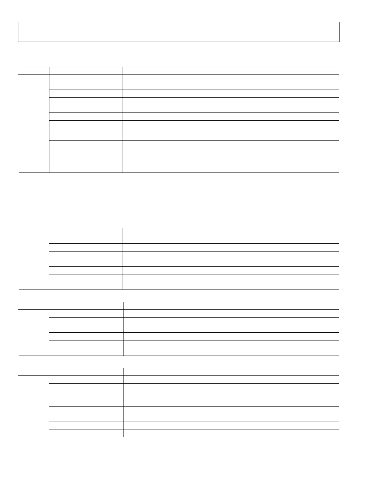
AD9558 Data Sheet
Reset Functions (Register 0x0A03)
Table 92. Reset Functions1
Address Bits Bit Name Description
0x0A03
(autoclear)
1
Note that all bits in this register are autoclearing.
IRQ Clearing (Register 0x0A04 to Register 0x0A09)
The IRQ clearing registers are identical in format to the IRQ monitor registers (Register 0x0D02 to Register 0x0D09). When set to logic 1,
an IRQ clearing bit resets the corresponding IRQ monitor bit, thereby canceling the interrupt request for the indicated event. The IRQ
clearing register is an autoclearing register.
7 Reserved Default: 0b.
6 Clear LF Setting this bit clears the digital loop filter (intended as a debug tool).
5 Clear CCI Setting this bit clears the CCI filter (intended as a debug tool).
4 Reserved Default: 0b.
3 Clear auto sync Setting this bit resets the automatic synchronization logic (see Register 0x0500).
2 Clear TW history Setting this bit resets the tuning word history logic (part of holdover functionality).
1 Clear all IRQs
0 Clear watchdog timer
Setting this bit clears the entire IRQ monitor register (Register 0x0D02 to Register 0x0D07).
It is the equivalent of setting all the bits of the IRQ clearing register (Register 0x0A04 to
Register 0x0A0D).
Setting this bit resets the watchdog timer (see Register 0x0211 and Register 0x0212). If the
timer times out, it starts a new timing cycle. If the timer has not yet timed out, it restarts at
time zero without causing a timeout event. Continuously resetting the watchdog timer at
intervals less than its timeout period prevents the watchdog timer from generating a timeout
event.
Table 93. IRQ Clearing for SYSCLK
Address Bits Bit Name Description
0x0A04
[7:6] Reserved Reserved
5 SYSCLK unlocked Clears SYSCLK unlocked IRQ
4 SYSCLK locked Clears SYSCLK locked IRQ
3 APLL unlocked Clears Output PLL unlocked IRQ
2 APLL locked Clears Output PLL locked IRQ
1 APLL Cal ended Clears APLL calibration complete IRQ
0 APLL Cal started Clears APLL calibration started IRQ
Table 94. IRQ Clearing for Distribution Sync, Watchdog Timer, and EEPROM
Address Bits Bit Name Description
0x0A05
[7:5] Reserved Reserved
4 Pin program end Clears pin program end IRQ
3 Sync clock distribution Clears distribution sync IRQ
2 Watchdog timer Clears watchdog timer IRQ
1 EEPROM fault Clears EEPROM fault IRQ
0 EEPROM complete Clears EEPROM complete IRQ
Table 95. IRQ Clearing for the Digital PLL
Address Bits Bit Name Description
0x0A06
7 Switching Clears switching IRQ
6 Closed Clears closed IRQ
5 Freerun Clears free run IRQ
4 Holdover Clears holdover IRQ
3 Frequency unlocked Clears frequency unlocked IRQ
2 Frequency locked Clears frequency locked IRQ
1 Phase unlocked Clears phase unlocked IRQ
0 Phase locked Clears phase locked IRQ
Rev. A | Page 90 of 104

Data Sheet AD9558
Table 96. IRQ Clearing for History Update, Frequency Limit, and Phase Slew Limit
Address Bits Bit Name Description
0x0A07
Table 97. IRQ Clearing for Reference Inputs
Address Bits Bit Name Description
0x0A08
0x0A09
[7:5] Reserved Reserved
4 History updated Clears history updated IRQ
3 Frequency unclamped Clears frequency unclamped IRQ
2 Frequency clamped Clears frequency clamped IRQ
1 Phase slew unlimited Clears phase slew unlimited IRQ
0 Phase slew limited Clears phase slew limited IRQ
7 Reserved Reserved
6 REFB validated Clears REFB validated IRQ
5 REFB fault cleared Clears REFB fault cleared IRQ
4 REFB fault Clears REFB fault IRQ
3 Reserved Reserved
2 REFA validated Clears REFA validated IRQ
1 REFA fault cleared Clears REFA fault cleared IRQ
0 REFA fault Clears REFA fault IRQ
7 Reserved Reserved
6 REFD validated Clears REFD validated IRQ
5 REFD fault cleared Clears REFD fault cleared IRQ
4 REFD fault Clears REFD fault IRQ
3 Reserved Reserved
2 REFC validated Clears REFC validated IRQ
1 REFC fault cleared Clears REFC fault cleared IRQ
0 REFC fault Clears REFC fault IRQ
Table 98. Incremental Phase Offset Control
Address Bits Bit Name Description
0x0A0A
[7:3] Reserved Reserved.
2 Reset phase offset
1 Decrement phase offset
0 Increment phase offset
Resets the incremental phase offset to zero.
This is an autoclearing bit.
Decrements the incremental phase offset by the amount specified in the incremental
phase lock offset step size registers (Register 0x0312 to Register 0x0313).
This is an autoclearing bit.
Increments the incremental phase offset by the amount specified in the incremental
phase lock offset step size registers (Register 0x0312 to Register 0x0313).
This is an autoclearing bit.
Table 99. Reference Validation Override Controls
Address Bits Bit Name Description
0x0A0B
0x0A0C
[7:4] Reserved Reserved.
3 Force Timeout D
2 Force Timeout C
1 Force Timeout B
0 Force Timeout A
[7:4] Reserved Reserved.
3 Ref Mon Override D Overrides the reference monitor REF FAULT signal for Reference D (default: 0).
2 Ref Mon Override C Overrides the reference monitor REF FAULT signal for Reference C (default: 0).
1 Ref Mon Override B Overrides the reference monitor REF FAULT signal for Reference B (default: 0).
0 Ref Mon Override A Overrides the reference monitor REF FAULT signal for Reference A (default: 0).
Setting this autoclearing bit emulates timeout of the validation timer for Reference D
and allows the user to make REFD valid immediately.
Setting this autoclearing bit emulates timeout of the validation timer for Reference C
and allows the user to make REFC valid immediately.
Setting this autoclearing bit emulates timeout of the validation timer for Reference B
and allows the user to make REFB valid immediately.
Setting this autoclearing bit emulates timeout of the validation timer for Reference A
and allows the user to make REFA valid immediately.
Rev. A | Page 91 of 104

AD9558 Data Sheet
Address Bits Bit Name Description
0x0A0D
QUICK IN/OUT FREQUENCY SOFT PIN CONFIGURATION (REGISTER 0x0C00 TO REGISTER 0x0C08)
Table 100. Soft Pin Program Setting1
Address Bits Bit Name Description
0x0C01
0x0C02 [7:2] Reserved Reserved.
[1:0]
1 0 0 24.576 MHz XTAL, ×2 on, N = 8
2 0 1 49.152 MHz XTAL, ×2 on, N = 8
3 1 0 24.576 MHz XO, ×2 off, N = 16
0x0C03 [7:1] Reserved Reserved.
0 Enable Soft Pin Section 2
0x0C04
[7:4] Reserved Reserved.
3 Ref Mon Bypass D Bypasses the reference monitor for Reference D (default: 0).
2 Ref Mon Bypass C Bypasses the reference monitor for Reference C (default: 0).
1 Ref Mon Bypass B Bypasses the reference monitor for Reference B (default: 0).
0 Ref Mon Bypass A Bypasses the reference monitor for Reference A (default: 0).
[7:1] Reserved Reserved. 0x0C00
0 Enable Soft Pin Section 1
[7:4] Output frequency selection
[3:0] Input frequency selection
System clock PLL ref
selection
[7:4] Reserved Reserved.
[3:2] REFB frequency scale Scales the the selected input frequency (defined by Register 0x0C01[3:0]) for REFB.
[1:0] REFA frequency scale Scales the the selected input frequency (defined by Register 0x0C01[3:0]) for REFA.
0 (default) = disables the function of soft pin registers in Soft Pin Section 1 (Register
0x0C01 and Register 0x0C02).
1 = enables the function of soft pin registers in Soft Pin Section 1 (Register 0x0C01 to
Register 0x0C02) when the PINCONTROL pin is low at startup and/or reset.
The register in Soft Pin Section 1 configures the part into one of 256 preconfigured
input-to-output frequency translations stored in the on-chip ROM.
The registers in Soft Pin Section 1 (Register 0x0C00 to Register 0x0C02) are ignored
when the PINCONTROL pin is high at power-up and/or reset (which means the hard pin
program is enabled).
Selects one of 16 predefined output frequencies as ouptut freqeuncy of the desired
frequency translation and reprograms the free run TW, N2, RF divider, and M0 to M3b
dividers with the value stored in the ROM.
Selects one of 16 predefined input frequencies as the input frequency of the desired
frequency translation and reprograms the reference period, R divider, N1, FRAC1, and
MOD1 in four REF profiles with the value stored in the ROM.
Selects one of the four predefined system PLL references for the desired frequency
translation and reprograms the system PLL configuration with the value stored in the
ROM. To load values from the ROM, the user must write Register 0x0C07[0] = 1 after writing
this.
Equivalent System Clock PLL Settings,
Register 0x0C02[1:0]
System PLL Ref
4 1 1 49.152 MHz XO, ×2 off, N = 8
0 (default) = disables the function of soft pin registers in Soft Pin Section 2 (Register
0x0C04 to Register 0x0C06).
1 = enables the function of soft pin registers in Soft Pin Section 2 (Register 0x0C04 to
Register 0x0C06) when PINCONTROL pin is low.
00 (default) = divide-by-1.
01 = divide-by-4.
10 = divide-by-8.
11 = divide-by-16.
For example, if the selected input frequency is 622.08 MHz and Register 0x0C04[3:2] =
11, the new input frequency should be 622.08 MHz/16 = 38.8 MHz
00 (default) = divide-by-1.
01 = divide-by-4.
10 = divide-by-8.
11 = divide-by-16.
Bit 1 Bit 0 12 Bits
Register 0x0100 to Register 0x101[3:0]
Rev. A | Page 92 of 104

Data Sheet AD9558
Address Bits Bit Name Description
0x0C05 [7:4] Reserved Reserved.
[3:2]
Channel 1 output frequency
scale
[1:0]
Channel 0 output frequency
scale
0x0C06 [7:5] Reserved Reserved.
4 Sel high PM base loop filter 0 = base loop filter with normal (70°) phase margin (default).
[3:2] DPLL loop BW Scale the DPLL loop BW while in soft pin mode.
[1:0]
Reference input frequency
tolerance
[7:1] Reserved Reserved. 0x0C07
0 Soft pin start transfer
[7:1] Reserved Reserved. 0x0C08
0 Soft pin reset
1
All bits in Register 0x0C00 to Register 0x0C06 take effect only with either a soft pin start transfer (Register 0x0C07) or soft pin reset (Register 0x0C08).
Scales the selected output frequency (defined by Register 0x0C01[7:4]) for the Channel
Divider 1 output.
00 (default) = divide-by-1.
01 = divide-by-4.
10 = divide-by-8.
11 = divide-by-16.
Scale the selected output frequency (defined by Register 0x0C01[7:4]) for the Channel
Divider 0 output.
00 (default) = divide-by-1.
01 = divide-by-4.
10 = divide-by-8.
11 = divide-by-16.
1 = base loop filter with high (88.5°) phase margin.
(< 0.1 dB peaking in closed-loop transfer function).
00 (default) = 50 Hz.
01 = 1 Hz.
10 = 10 Hz.
11 =100 Hz.
Scales the input frequency tolerance while in soft pin mode.
00 (default) = outer tolerance: 10%; inner tolerance: 8% (for general conditions).
01 = outer tolerance: 12 ppm; inner tolerance: 9.6 ppm (for Stratum 3).
10 = outer tolerance: 48 ppm; inner tolerance: 38 ppm (for SMC clock standard).
11 = outer tolerance: 200 ppm; inner tolerance: 160 ppm (for XTAL system clock).
Autoclearing register. 1 = initiates ROM download without resetting the part/register map.
After ROM download is complete, this register is reset.
Autoclearing register; resets the part like soft reset (Register 0x0000[5]), except that this
reset function initiates a soft pin ROM download without resetting the part/register map.
After ROM download is complete, this register is pulled back to zero.
STATUS READBACK (REGISTER 0x0D00 TO REGISTER 0x0D14)
All bits in Register 0x0D00 to Register 0x0D14 are read only. To show the latest status, these registers require an I/O update (Register 0x0005 =
0x01) immediately before being read.
Table 101. EEPROM Status
Address Bits Bit Name Description
0x0D00
[7:4] Reserved Reserved.
3 Pin program ROM load process The control logic sets this bit when data is being read from the ROM.
2 Fault detected An error occurred while saving data to or loading data from the EEPROM.
1 Load in progress The control logic sets this bit while data is being read from the EEPROM.
0 Save in progress The control logic sets this bit while data is being written to the EEPROM.
Rev. A | Page 93 of 104
AD9558 Data Sheet
Table 102. SYSCLK Status
Address Bits Bit Name Description
0x0D01
7 Reserved Reserved.
6 DPLL_APLL_Lock
5 All PLLs locked
4 APLL VCO status
3 APLL cal in process The control logic holds this bit set while the amplitude calibration of the APLL VCO is in progress.
2 APLL lock
1 System clock stable
0 SYSCLK lock detect
Indicates the status of the DPLL and APLL.
0 = either the DPLL or the APLL is unlocked.
1 = both the DPLL and APLL are locked.
Indicates the status of the system clock PLL, APLL, and DPLL.
0 = system clock PLL or APLL or DPLL is unlocked.
1 = all three PLLs (system clock PLL, APLL, and DPLL) are locked.
1 = OK.
0 = off/clocks are missing.
Indicates the status of the APLL.
0 = unlocked.
1 = locked.
The control logic sets this bit when the device considers the system clock to be stable (see
the System Clock Stability Timer section).
0 = not stable (the system clock stability timer has not expired yet).
1 = stable (the system clock stability timer has expired).
Indicates the status of the system clock PLL.
0 = unlocked.
1 = locked.
IRQ Monitor (Register 0x0D02 to Register 0x0D09)
If not masked via the IRQ mask registers (Register 0x0209 to Register 0x020F), the appropriate IRQ monitor bit is set to a Logic 1 when
the indicated event occurs. These bits can be cleared only via the IRQ clearing registers (Register 0x0A04 to Register 0x0A09), the reset all
IRQs bit (Register 0x0A03[1]), or a device reset.
Table 103. IRQ Monitor for SYSCLK
Address Bits Bit Name Description
0x0D02
[7:6] Reserved Reserved
5 SYSCLK unlocked Indicates a SYSCLK PLL state transition from locked to unlocked
4 SYSCLK locked Indicates a SYSCLK PLL state transition from unlocked to locked
3 APLL unlocked Indicates an output PLL state transition from locked to unlocked
2 APLL locked Indicates an output PLL state transition from unlocked to locked
1 APLL cal ended Indicates that APLL calibration is complete
0 APLL cal started Indicates that APLL in APLL calibration has begun
Table 104. IRQ Monitor for Distribution Sync, Watchdog Timer, and EEPROM
Address Bit Bit Name Description
0x0D03
[7:5] Reserved Reserved
4 Pin program end Indicates successful completion of a ROM load operation
3 Output distribution sync Indicates a distribution sync event
2 Watchdog timer Indicates expiration of the watchdog timer
1 EEPROM fault Indicates a fault during an EEPROM load or save operation
0 EEPROM complete Indicates successful completion of an EEPROM load or save operation
Rev. A | Page 94 of 104

Data Sheet AD9558
Table 105. IRQ Monitor for the Digital PLL
Address Bits Bit Name Description
0x0D04
Table 106. IRQ Monitor for History Update, Frequency Limit, and Phase Slew Limit
Address Bits Bit Name Description
0x0D05
Table 107. IRQ Monitor for Reference Inputs
Address Bits Bit Name Description
0x0D06
0x0D07
7 Switching Indicates that the DPLL is switching to a new reference
6 Closed Indicates that the DPLL has entered closed-loop operation
5 Freerun Indicates that the DPLL has entered free run mode
4 Holdover Indicates that the DPLL has entered holdover mode
3 Frequency unlocked Indicates that the DPLL has lost frequency lock
2 Frequency locked Indicates that the DPLL has acquired frequency lock
1 Phase unlocked Indicates that the DPLL has lost phase lock
0 Phase locked Indicates that the DPLL has acquired phase lock
[7:5] Reserved Reserved
4 History updated Indicates the occurrence of a tuning word history update
3 Frequency unclamped Indicates a frequency limiter state transition from clamped to unclamped
2 Frequency clamped Indicates a frequency limiter state transition from unclamped to clamped
1 Phase slew unlimited Indicates a phase slew limiter state transition from slew limiting to not slew limiting
0 Phase slew limited Indicates a phase slew limiter state transition from not slew limiting to slew limiting
7 Reserved Reserved
6 REFB validated Indicates that REFB has been validated
5 REFB fault cleared Indicates that REFB has been cleared of a previous fault
4 REFB fault Indicates that REFB has been faulted
3 Reserved Reserved
2 REFA validated Indicates that REFA has been validated
1 REFA fault cleared Indicates that REFA has been cleared of a previous fault
0 REFA fault Indicates that REFA has been faulted
7 Reserved Reserved
6 REFD validated Indicates that REFD has been validated
5 REFD fault cleared Indicates that REFD has been cleared of a previous fault
4 REFD fault Indicates that REFD has been faulted
3 Reserved
2 REFC validated Indicates that REFC has been validated
1 REFC fault cleared Indicates that REFC has been cleared of a previous fault
0 REFC fault Indicates that REFC has been faulted
Rev. A | Page 95 of 104

AD9558 Data Sheet
DPLL Status, Input Reference Status, Holdover History, and DPLL Lock Detect Tub Levels (Register 0x0D08 to Register 0x0D14)
Table 108. DPLL Status1
Address Bits Bit Name Description
0x0D08
0x0D09 [7:6] Reserved Default: 0b
5 Frequency clamped The upper or lower frequency tuning word clamp is in effect
4 History available There is sufficient tuning word history available for holdover operation
1
Note that the user must issue an I/O update by writing 0x01 to Register 0x0005 to update the status of these registers.
7 Reserved Reserved
6 Offset slew limiting The current closed-loop phase offset is rate limited
5 Frequency lock The DPLL has achieved frequency lock
4 Phase lock The DPLL has achieved phase lock
3 Loop switching The DPLL is in the process of a reference switchover
2 Holdover The DPLL is in holdover mode
1 Active The DPLL is active (that is, operating in a closed-loop condition)
0 Freerun The DPLL is free run (that is, operating in an open-loop condition)
[3:2] Active reference priority Priority value of the currently active reference
00 = highest priority
…
11 = lowest priority
[1:0] Current active reference Index of the currently active reference
00 = Reference A
01 = Reference B
10 = Reference C
11 = Reference D
Table 109. Reserved Register
Address Bits Bit Name Description
0x0D0A [7:0] Reserved Reserved.
Table 110. Input Reference Status1
Address Bits Bit Name Description
0x0D0B
7 B valid REFB is valid for use. (It is unfaulted, and its validation timer has expired.)
6 B fault REFB is not valid for use.
5 B fast This bit indicates that the frequency of REFB is higher than allowed by its profile settings.
4 B slow This bit indicates that the frequency of REFB is lower than allowed by its profile settings.
3 A valid REFA is valid for use. (It is unfaulted, and its validation timer has expired.)
2 A fault REFA is not valid for use.
1 A fast This bit indicates that the frequency of REFA is higher than allowed by its profile settings.
0 A slow This bit indicates that the frequency of REFA is lower than allowed by its profile settings.
[7:4] Same as Register 0xDOB[7:4] but for REFD instead of REFB . 0x0D0C
1
Note that the user must issue an I/O update by writing 0x01 to Register 0x0005 to update the status of these registers.
[3:0] Same as Register 0xDOB[3:0] but for REFC instead of REFA.
Table 111. Holdover History1
Address Bits Bit Name Description
0x0D0D [7:0] Tuning word readback bits[7:0]
0x0D0E [7:0]
0x0D0F [7:0] Tuning word readback bits[23:9]
0x0D10 [7:0]
1
Note that these registers contain the current 30-bit DCO frequency tuning word generated by the tuning word history logic.
Holdover history
Tuning word readback bits[15:8]
Tuning word readback bits[29:24]
Rev. A | Page 96 of 104
Data Sheet AD9558
Table 112. Digital PLL Lock Detect Tub Levels1
Address Bits Bit Name Description
0x0D11 [7:0]
0x0D12 [7:4] Reserved.
[3:0]
0x0D13 [7:0] Frequency tub
0x0D14 [7:4] Reserved Reserved.
[3:0] Frequency tub
1
These registers contain the current digital PLL lock detection bathtub levels.
EEPROM CONTROL (REGISTER 0x0E00 TO REGISTER 0x0E03)
Table 113. EEPROM Control
Address Bits Bit Name Description
[7:1] Reserved Reserved. 0x0E00
0 Write enable EEPROM write enable/protect.
[7:4] Reserved Reserved. 0x0E01
[3:0] Conditional value When set to a non-zero value, it establishes the condition for EEPROM downloads. Default: 0b.
[7:1] Reserved Reserved. 0x0E02
0 Save to EEPROM
0x0E03
[7:2] Reserved Reserved.
1 Load from EPROM Downloads data from the EEPROM.
0 Reserved Reserved.
Phase tub
Read-only digital PLL lock detect bathtub level, Bits[7:0]; see the DPLL Frequency Lock Detector
section for details.
Read-only digital PLL lock detect bathtub level, Bits[11:8]; see the DPLL Frequency Lock
Detector section for details.
Read-only digital PLL lock detect bathtub level, Bits[7:0]; see the DPLL Phase Lock Detector
section for details.
Read-only digital PLL lock detect bathtub level, Bits[11:8]; see the DPLL Phase Lock Detector
section for details.
0 (default) = EEPROM write protected.
1 = EEPROM write enabled.
Upload data to the EEPROM based on the EEPROM Storage Sequence (Register 0x0E10 to
Register 0x0E3C) section.
Rev. A | Page 97 of 104

AD9558 Data Sheet
EEPROM STORAGE SEQUENCE (REGISTER 0x0E10 TO REGISTER 0x0E3C)
The default settings of Register 0x0E10 to Register 0x0E3C contain the default EEPROM instruction sequence. The tables in this section
provide descriptions of the register defaults, based on the assumption that the controller has been instructed to carry out an EEPROM
storage sequence in which all of the registers are stored and loaded by the EEPROM.
Table 114. EEPROM Storage Sequence for System Clock Settings
Address Bits Bit Name Description
0x0E10 [7:0]
0x0E11 [7:0]
0x0E12 [7:0]
0x0E13 [7:0]
0x0E14 [7:0]
0x0E15 [7:0]
0x0E16 [7:0] I/O update
EEPROM ID
System clock
The default value of this register is 0x01, which the controller interprets as a data instruction. Its decimal
value is 1, so this tells the controller to transfer two bytes of data (1 + 1), beginning at the address that is
specified by the next two bytes. The controller stores 0x01 in the EEPROM and increments the EEPROM
address pointer.
The default value of these two registers is 0x0006. Note that Register 0x0E11 and Register 0x0E12 are
the most significant and least significant bytes of the target address, respectively. Because the previous
register contains a data instruction, these two registers define a starting address (in this case, 0x0006).
The controller stores 0x0006 in the EEPROM and increments the EEPROM pointer by 2. It then transfers
two bytes from the register map (beginning at Address 0x0006) to the EEPROM and increments the
EEPROM address pointer by 3 (two data bytes and one checksum byte). The two bytes transferred
correspond to the system clock parameters in the register map.
The default value of this register is 0x08, which the controller interprets as a data instruction. Its decimal
value is 8, so this tells the controller to transfer nine bytes of data (8 + 1), beginning at the address that
is specified by the next two bytes. The controller stores 0x08 in the EEPROM and increments the
EEPROM address pointer.
The default value of these two registers is 0x0100. Note that Register 0x0E14 and Register 0x0E15 are
the most significant and least significant bytes of the target address, respectively. Because the previous
register contains a data instruction, these two registers define a starting address (in this case, 0x0100).
The controller stores 0x0100 in the EEPROM and increments the EEPROM pointer by 2. It then transfers
nine bytes from the register map (beginning at Address 0x0100) to the EEPROM and increments the
EEPROM address pointer by 10 (nine data bytes and one checksum byte). The nine bytes transferred
correspond to the system clock parameters in the register map.
The default value of this register is 0x80, which the controller interprets as an I/O update instruction.
The controller stores 0x80 in the EEPROM and increments the EEPROM address pointer.
Table 115. EEPROM Storage Sequence for General Configuration Settings
Address Bits Bit Name Description
0x0E17 [7:0] General
0x0E18 [7:0]
0x0E19 [7:0]
The default value of this register is 0x11, which the controller interprets as a data instruction. Its decimal
value is 17, which tells the controller to transfer 18 bytes of data (17 + 1), beginning at the address that
is specified by the next two bytes. The controller stores 0x11 in the EEPROM and increments the
EEPROM address pointer.
The default value of these two registers is 0x0200. Note that Register 0x0E18 and Register 0x0E19 are
the most significant and least significant bytes of the target address, respectively. Because the previous
register contains a data instruction, these two registers define a starting address (in this case, 0x0200).
The controller stores 0x0200 in the EEPROM and increments the EEPROM pointer by 2. It then transfers
18 bytes from the register map (beginning at Address 0x0200) to the EEPROM and increments the EEPROM
address pointer by 19 (18 data bytes and one checksum byte). The 18 bytes transferred correspond to
the general configuration parameters in the register map.
Table 116. EEPROM Storage Sequence for DPLL Settings
Address Bits Bit Name Description
0x0E1A [7:0] DPLL
0x0E1B [7:0]
0x0E1C [7:0]
The default value of this register is 0x2E, which the controller interprets as a data instruction. Its decimal
value is 46, which tells the controller to transfer 47 bytes of data (46 + 1), beginning at the address that
is specified by the next two bytes. The controller stores 0x2E in the EEPROM and increments the EEPROM
address pointer.
The default value of these two registers is 0x03. Note that Register 0x0E1B and Register 0x0E1C are the
most significant and least significant bytes of the target address, respectively. Because the previous
register contains a data instruction, these two registers define a starting address (in this case, 0x0300).
The controller stores 0x0300 in the EEPROM and increments the EEPROM pointer by 2. It then transfers
47 bytes from the register map (beginning at Address 0x0300) to the EEPROM and increments the EEPROM
address pointer by 48 (47 data bytes and one checksum byte). The 47 bytes transferred correspond to
the DPLL parameters in the register map.
Rev. A | Page 98 of 104

Data Sheet AD9558
Table 117. EEPROM Storage Sequence for Output PLL Settings
Address Bits Bit Name Description
0x0E1D [7:0] APLL
0x0E1E [7:0]
0x0E1F [7:0]
Table 118. EEPROM Storage Sequence for Clock Distribution Settings
Address Bits Bit Name Description
0x0E20 [7:0] Clock distribution
0x0E21 [7:0]
0x0E22 [7:0]
0x0E23 [7:0] I/O update
The default value of this register is 0x08, which the controller interprets as a data instruction. Its
decimal value is 8, which tells the controller to transfer nine bytes of data (8 + 1), beginning at the
address that is specified by the next two bytes. The controller stores 0x08 in the EEPROM and
increments the EEPROM address pointer.
The default value of these two registers is 0x0400. Note that Register 0x0E1E and Register 0x0E1F
are the most significant and least significant bytes of the target address, respectively. Because the
previous register contains a data instruction, these two registers define a starting address (in this
case, 0x0400). The controller stores 0x0400 in the EEPROM and increments the EEPROM pointer by 2.
It then transfers nine bytes from the register map (beginning at Address 0x0400) to the EEPROM
and increments the EEPROM address pointer by 10 (nine data bytes and one checksum byte). The
nine bytes transferred correspond to APLL parameters in the register map.
The default value of this register is 0x15, which the controller interprets as a data instruction. Its
decimal value is 21, which tells the controller to transfer 22 bytes of data (21+1), beginning at the
address that is specified by the next two bytes. The controller stores 0x15 in the EEPROM and
increments the EEPROM address pointer.
The default value of these two registers is 0x0500. Note that Register 0x0E21 and Register 0x0E22
are the most significant and least significant bytes of the target address, respectively. Because the
previous register contains a data instruction, these two registers define a starting address (in this
case, 0x0500). The controller stores 0x0500 in the EEPROM and increments the EEPROM pointer by 2.
It then transfers 22 bytes from the register map (beginning at Address 0x0500) to the EEPROM and
increments the EEPROM address pointer by 23 (22 data bytes and one checksum byte). The
22 bytes transferred correspond to the clock distribution parameters in the register map.
The default value of this register is 0x80, which the controller interprets as an I/O update
instruction. The controller stores 0x80 in the EEPROM and increments the EEPROM address
pointer.
Table 119. EEPROM Storage Sequence for Reference Input Settings
Address Bits Bit Name Description
0x0E24 [7:0] Reference inputs
0x0E25 [7:0]
0x0E26 [7:0]
The default value of this register is 0x03, which the controller interprets as a data instruction. Its
decimal value is 3, so this tells the controller to transfer four bytes of data (3 + 1), beginning at the
address that is specified by the next two bytes. The controller stores 0x03 in the EEPROM and
increments the EEPROM address pointer.
The default value of these two registers is 0x0600. Note that Register 0x0E25 and Register 0x0E26
are the most significant and least significant bytes of the target address, respectively. Because the
previous register contains a data instruction, these two registers define a starting address (in this
case, 0x0600). The controller stores 0x0600 in the EEPROM and increments the EEPROM pointer by 2.
It then transfers four bytes from the register map (beginning at Address 0x0600) to the EEPROM
and increments the EEPROM address pointer by 5 (four data bytes and one checksum byte). The
four bytes that are transferred correspond to the reference inputs parameters in the register map.
Table 120. EEPROM Storage Sequence for Frame Sync Settings
Address Bit Bit Name Description
0x0E27 [7:0] Frame sync
0x0E28 [7:0]
0x0E29 [7:0]
The default value of this register is 0x01, which the controller interprets as a data instruction. Its
decimal value is 1, which tells the controller to transfer two bytes of data (1 + 1), beginning at the
address specified by the next two bytes. The controller stores 0x01 in the EEPROM and increments
the EEPROM address pointer.
The default value of these two registers is 0x0640. Note that Register 0x0E28 and Register 0x0E29
are the most significant and least significant bytes of the target address, respectively. Because the
previous register contains a data instruction, these two registers define a starting address (in this
case, 0x0640). The controller stores 0x0640 in the EEPROM and increments the EEPROM pointer by 2.
It then transfers two bytes from the register map (beginning at Address 0x0640) to the EEPROM
and increments the EEPROM address pointer by 3 (two data bytes and one checksum byte). The
two bytes transferred correspond to the reference inputs parameters in the register map.
Rev. A | Page 99 of 104
AD9558 Data Sheet
Table 121. EEPROM Storage Sequence for REFA Profile Settings
Address Bits Bit Name Description
0x0E2A [7:0]
0x0E2B [7:0]
0x0E2C [7:0]
Table 122. EEPROM Storage Sequence for REFB Profile Settings
Address Bits Bit Name Description
0x0E2D [7:0]
0x0E2E [7:0]
0x0E2F [7:0]
REFA Profile
REFB profile
The default value of this register is 0x26, which the controller interprets as a data instruction. Its decimal
value is 38, so this tells the controller to transfer 39 bytes of data (38 + 1), beginning at the address that
is specified by the next two bytes. The controller stores 0x26 in the EEPROM and increments the EEPROM
address pointer.
The default value of these two registers is 0x0700. Note that Register 0x0E2B and Register 0x0E2C are
the most significant and least significant bytes of the target address, respectively. Because the previous
register contains a data instruction, these two registers define a starting address (in this case, 0x0700).
The controller stores 0x0700 in the EEPROM and increments the EEPROM pointer by 2. It then transfers
39 bytes from the register map (beginning at Address 0x0700) to the EEPROM and increments the
EEPROM address pointer by 40 (39 data bytes and one checksum byte). The 39 bytes transferred
correspond to the REFA profile parameters in the register map.
The default value of this register is 0x26, which the controller interprets as a data instruction. Its decimal
value is 38, so this tells the controller to transfer 39 bytes of data (38 + 1), beginning at the address that is
specified by the next two bytes. The controller stores 0x26 in the EEPROM and increments the EEPROM
address pointer.
The default value of these two registers is 0x0740. Note that Register 0x0E2E and Register 0x0E2F are the
most significant and least significant bytes of the target address, respectively. Because the previous register
contains a data instruction, these two registers define a starting address (in this case, 0x0740). The controller
stores 0x0740 in the EEPROM and increments the EEPROM pointer by 2. It then transfers 39 bytes from the
register map (beginning at Address 0x0740) to the EEPROM and increments the EEPROM address pointer
by 40 (39 data bytes and one checksum byte). The 39 bytes transferred correspond to the REFB profile
parameters in the register map.
Table 123. EEPROM Storage Sequence for REFC Profile Settings
Address Bits Bit Name Description
0x0E30 [7:0]
0x0E31 [7:0]
0x0E32 [7:0]
REFC profile
The default value of this register is 0x26, which the controller interprets as a data instruction. Its decimal
value is 38, so this tells the controller to transfer 39 bytes of data (38 + 1), beginning at the address that is
specified by the next two bytes. The controller stores 0x26 in the EEPROM and increments the EEPROM
address pointer.
The default value of these two registers is 0x0780. Note that Register 0x0E31 and Register 0x0E32 are
the most significant and least significant bytes of the target address, respectively. Because the previous
register contains a data instruction, these two registers define a starting address (in this case, 0x0780).
The controller stores 0x0780 in the EEPROM and increments the EEPROM pointer by 2. It then transfers
39 bytes from the register map (beginning at Address 0x0780) to the EEPROM and increments the
EEPROM address pointer by 40 (39 data bytes and one checksum byte). The 39 bytes transferred
correspond to the REFC profile parameters in the register map.
Table 124. EEPROM Storage Sequence for REFD Profile Settings
Address Bits Bit Name Description
0x0E33 [7:0]
0x0E34 [7:0]
0x0E35 [7:0]
REFD profile
The default value of this register is 0x26, which the controller interprets as a data instruction. Its decimal
value is 38, so this tells the controller to transfer 39 bytes of data (38 + 1), beginning at the address that is
specified by the next two bytes. The controller stores 0x26 in the EEPROM and increments the EEPROM
address pointer.
The default value of these two registers is 0x07C0. Note that Register 0x0E34 and Register 0x0E35 are
the most significant and least significant bytes of the target address, respectively. Because the previous
register contains a data instruction, these two registers define a starting address (in this case, 0x07C0).
The controller stores 0x07C0 in the EEPROM and increments the EEPROM pointer by 2. It then transfers
39 bytes from the register map (beginning at Address 0x07C0) to the EEPROM and increments the EEPROM
address pointer by 40 (39 data bytes and one checksum byte). The 39 bytes transferred correspond to
the REFD profile parameters in the register map.
Rev. A | Page 100 of 104
 Loading...