

X
Oscillator Frequency Upconverter
FEATURES
Converts a low frequency input reference signal to a high
frequency output signal
Input frequencies from 6.6 MHz to 112.5 MHz
Output frequencies up to 900 MHz
Preset pin programmable frequency translation ratios
Arbitrary frequency translation ratios via SPI port
On-chip VCO
Accepts a crystal resonator and/or an external oscillator
as a reference frequency source
Secondary output (either integer-related to the primary
output or a copy of the reference input)
RMS jitter: <0.5 ps
SPI-compatible, 3-wire programming interface
Single supply (3.3 V)
Very low power: <400 mW (under most conditions)
Small package size (5 mm × 5 mm)
APPLICATIONS
Cost effective replacement of high frequency VCXO, OCXO,
and SAW resonators
Extremely flexible frequency translation with low jitter for
SONET/SDH (including FEC), 10 Gb Ethernet, Fibre
Channel, and DRFI/DOCSIS
High-definition video frequency translation
Wireless infrastructure
Test and measurement (including handheld devices)
AD9552
GENERAL DESCRIPTION
The AD9552 is a fractional-N phase locked loop (PLL) based
clock generator designed specifically to replace high frequency
crystal oscillators and resonators. The device employs a sigmadelta (Σ-) modulator (SDM) to accommodate fractional
frequency synthesis. The user supplies an input reference signal
by connecting a single-ended clock signal directly to the REF
pin or by connecting a crystal resonator across the XTAL pins.
The AD9552 is pin programmable, providing one of 64 standard
output frequencies based on one of eight common input
frequencies. The device also has a 3-wire SPI interface, enabling
the user to program custom input-to-output frequency ratios.
The AD9552 relies on an external capacitor to complete the loop
filter of the PLL. The output is compatible with LVPECL, LVDS,
or single-ended CMOS logic levels, although the AD9552 is
implemented in a strictly CMOS process.
The AD9552 is specified to operate over the extended industrial
temperature range of −40°C to +85°C.
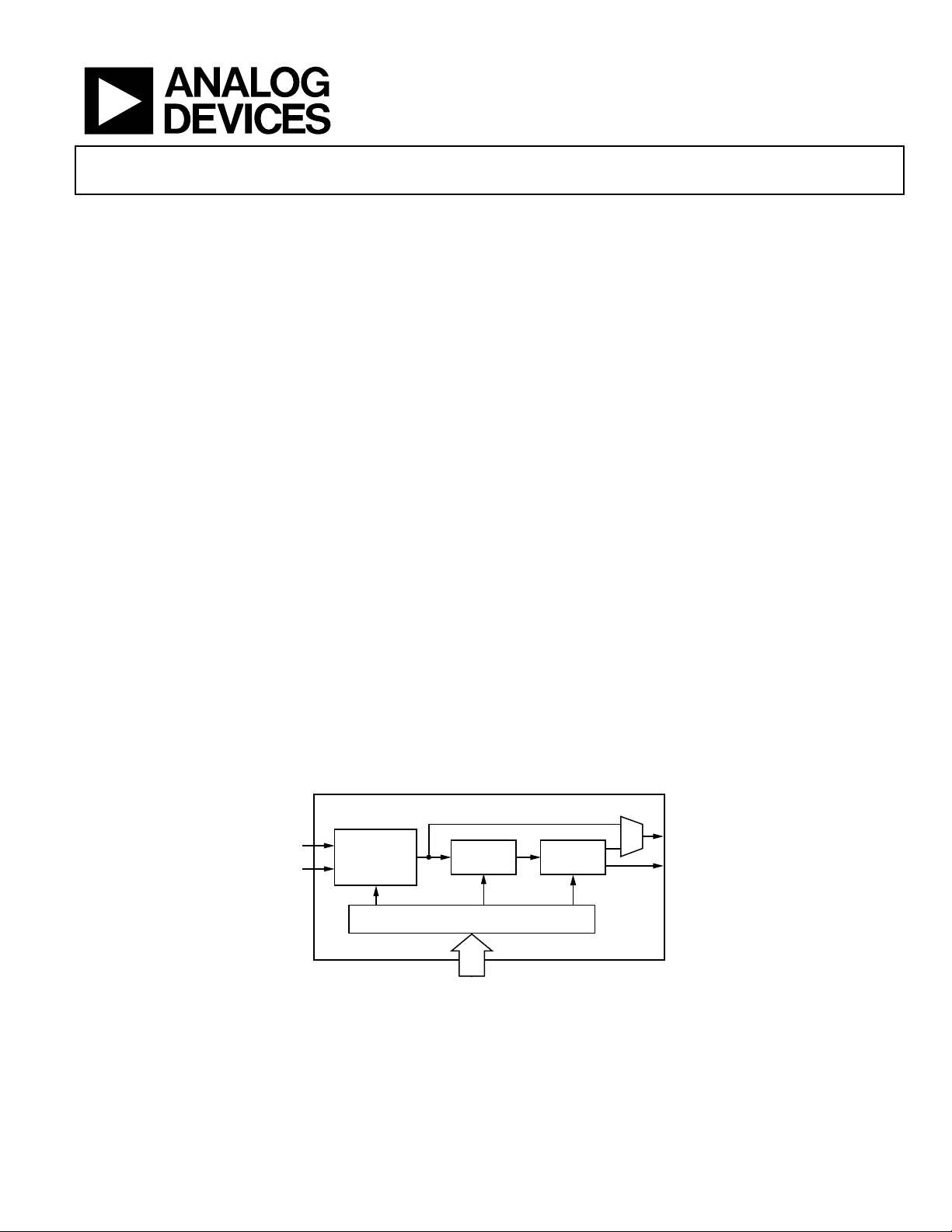
BASIC BLOCK DIAGRAM
REF
TAL
Rev. D
Information furnished by Analog Devices is believed to be accurate and reliable. However, no
responsibility is assumed by Anal og Devices for its use, nor for any infringements of patents or ot her
rights of third parties that may result from its use. Specifications subject to change without notice. No
license is granted by implication or otherwise under any patent or patent rights of Analog Devices.
Trademarks and registered trademarks are the property of their respective owners.
INPUT
FREQUENCY
SOURCE
SELECTOR
PIN-DEFINE D AND SERIAL PROGRAM MING
AD9552
PLL
Figure 1.
OUTPUT
CIRCUITRY
One Technology Way, P.O. Box 9106, Norwood, MA 02062-9106, U.S.A.
Tel: 781.329.4700 www.analog.com
Fax: 781.461.3113 ©2009–2011 Analog Devices, Inc. All rights reserved.
OUT2
OUT1
07806-001

AD9552
TABLE OF CONTENTS
Features.............................................................................................. 1
Applications....................................................................................... 1
General Description ......................................................................... 1
Basic Block Diagram ........................................................................ 1
Revision History ............................................................................... 2
Specifications..................................................................................... 3
Crystal Input Characteristics ...................................................... 4
Output Characteristics................................................................. 4
Jitter Characteristics..................................................................... 5
Serial Control Port ....................................................................... 6
Serial Control Port Timing .........................................................6
Absolute Maximum Ratings............................................................ 7
ESD Caution.................................................................................. 7
Pin Configuration and Function Descriptions............................. 8
Typical Performance Characteristics ............................................. 9
Input/Output Termination Recommendations.......................... 12
Theory of Operation ...................................................................... 13
Preset Frequency Ratios ............................................................ 13
Component Blocks..................................................................... 15
Part Initialization and Automatic Power-On Reset............... 17
Output/Input Frequency Relationship .................................... 17
Calculating Divider Values ....................................................... 17
Low Dropout (LDO) Regulators.............................................. 18
Applications Information.............................................................. 19
Thermal Performance................................................................ 19
Serial Control Port ......................................................................... 20
Serial Control Port Pin Descriptions....................................... 20
Operation of the Serial Control Port....................................... 20
Instruction Word (16 Bits)........................................................ 21
MSB/LSB First Transfers ........................................................... 21
Register Map ................................................................................... 24
Register Map Descriptions........................................................ 25
Outline Dimensions....................................................................... 31
Ordering Guide .......................................................................... 31
REVISION HISTORY
7/11—Rev. C to Rev. D
Changes to Table 1, Reference Clock Input Characteristics,
Input High Voltage and Input Low Voltage Parameter Values... 4
Changes to Table 8, Added Endnote for Pin 9 and Pin 10.......... 8
Changes to Part Initialization Automatic Power-On Reset
Section, Second Paragraph............................................................ 17
Changes to Thermal Performance Section , First Paragraph ... 19
Changes to Serial Port Control Section, First Paragraph.......... 20
Changes to Table 20, Added Endnote to Bit 2 Description ...... 27
Updated Outline Dimensions....................................................... 31
7/10—Rev. B to Rev. C
Changed Crystal Load Capacitance to 15 pF............. Throughout
Added Conditions Statement to Specifications Section, Supply
Voltage Specifications, and Input Voltage Specifications............ 3
Reformatted Specifications Section (Renumbered Sequentially).....3
Added Input/Output Termination Recommendations Section,
Figure 17, and Figure 18 (Renumbered Sequentially)............... 13
Moved Preset Frequency Ratios Section ..................................... 13
Changes to Component Blocks Section ...................................... 15
Added Part Initialization and Automatic Power-On
Reset Section ................................................................................... 17
4/10—Rev. A to Rev. B
Changes to Preset Frequency Ratios Section.............................. 12
Moved Table 15 and Changes to Table 15................................... 13
Changes to Figure 17...................................................................... 14
Changes to PLL Section, Output Dividers Section, and
Input-to-OUT2 Option Section............................................... 15
Changes to Output/Input Frequency Relationship Section...... 16
Changes to Table 22 ....................................................................... 23
Changes to Table 26 ....................................................................... 26
9/09—Rev. 0 to Rev. A
Changes to Table 4.............................................................................3
Changes to Table 5.............................................................................4
Added Table 6; Renumbered Sequentially .....................................4
Changes to Figure 5...........................................................................9
Changes to PLL Section................................................................. 14
Changes to Table 22 ....................................................................... 21
Changes to Table 25 ....................................................................... 24
7/09—Revision 0: Initial Version
Rev. D | Page 2 of 32

AD9552
SPECIFICATIONS
Minimum (min) and maximum (max) values apply for the full range of supply voltage and operating temperature variations. Typical (typ)
values apply for VDD = 3.3 V; T
Table 1.
Parameter Min Typ Max Unit Test Conditions/Comments
SUPPLY VOLTAGE 3.135 3.30 3.465 V Pin 7, Pin 18, Pin 21, Pin 28
POWER CONSUMPTION
Total Current 149 169 mA At maximum output frequency with both output channels active
VDD Current By Pin
Pin 7 2 3 mA
Pin 18 77 86 mA
Pin 21 35 41 mA
Pin 28 35 41 mA
LVPECL Output Driver 36 41 mA
LOGIC INPUT PINS
INPUT CHARACTERISTICS1
Logic 1 Voltage, VIH 1.0 V
Logic 0 Voltage, VIL 0.8 V
Logic 1 Current, IIH 3 µA
Logic 0 Current, IIL 17 µA
LOGIC OUTPUT PINS
Output Characteristics
Output Voltage High, VOH 2.7 V
Output Voltage Low, VOL 0.4 V
RESET PIN
Input Characteristics2
Input Voltage High, VIH 1.8 V
Input Voltage Low, VIL 1.3 V
Input Current High, I
Input Current Low, I
INH
INL
Minimum Pulse Width High 2 ns
REFERENCE CLOCK
INPUT CHARACTERISTICS
Frequency Range 7.94 MHz N3 = 255; 2× frequency multiplier enabled; valid for all VCO bands
6.57 MHz
93.06 MHz SDM4 disabled; N3 = 365; valid for all VCO bands
71.28 MHz SDM4 enabled; N3 = 476; valid for all VCO bands
112.5 MHz
86.17 MHz
= 25°C, unless otherwise noted.
A
900 MHz with 100 Ω termination between both pins of the output
driver
For the CMOS inputs, a static Logic 1 results from either a pull-up
resistor or no connection
0.3 12.5 µA
31 43 µA
3
= 255; 2× frequency multiplier enabled; f
N
strains the frequency at OUT1 to be an integer sub-multiple of 3.35 GHz
(that is, f
output divider values)
4
SDM
frequency at OUT1 to be an integer sub-multiple of 4.05 GHz (that is,
f
= 4.05÷M GHz, where M is the product of the P0 and P1 output
OUT1
divider values)
4
SDM
at OUT1 to be an integer sub-multiple of 4.05 GHz (that is, f
4.05÷M GHz, where M is the product of the P
values)
= 3.35 GHz, which con-
VCO
= 3.35 ÷ M GHz, where M is the product of the P0 and P1
OUT1
disabled; N3 = 365; f
enabled; N3 = 476; f
= 4.05 GHz, which constrains the
VCO
= 4.05 GHz, which constrains the frequency
VCO
and P1 output divider
0
OUT1
=
Rev. D | Page 3 of 32
AD9552
Parameter Min Typ Max Unit Test Conditions/Comments
Input Capacitance 3 pF
Input Resistance 130 kΩ
Duty Cycle 40 60 %
Input Voltage
Input High Voltage, VIH 1.62 V
Input Low Voltage, VIL 0.52 V
Input Threshold Voltage 1.0 V
VCO CHARACTERISTICS
Frequency Range
Upper Bound 4050 MHz
Lower Bound 3350 MHz
VCO Gain 45 MHz/V
VCO Tracking Range ±300 ppm
VCO Calibration Time 140 s
1
The A[2:0], Y[5:0], and OUTSEL pins have 100 kΩ internal pull-up resistors.
2
The RESET pin has a 100 kΩ internal pull-up resistor, so the default state of the device is reset.
3
N is the integer part of the feedback divider.
4
Sigma-delta modulator.
5
The minimum allowable feedback divider value with the SDM disabled.
6
The minimum allowable feedback divider value with the SDM enabled.
7
The frequency at the input to the phase-frequency detector.
When ac coupling to the input receiver, the user must dc bias the input
to 1 V
7
= 77.76 MHz; time between completion of the VCO calibration
f
PFD
command (the rising edge of CS
(Pin 12)) to the rising edge of LOCKED
(Pin 20).
CRYSTAL INPUT CHARACTERISTICS
Table 2.
Parameter Min Typ Max Unit Test Conditions/Comments
CRYSTAL FREQUENCY
Range 10 26 52 MHz
Tolerance 20 ppm
CRYSTAL MOTIONAL RESISTANCE 100 Ω
CRYSTAL LOAD CAPACITANCE 15 pF
Using a crystal with a specified load capacitance other than
15 pF (8 pF to 24 pF) is possible, but necessitates using the
SPI port to configure the AD9552 crystal input capacitance.
OUTPUT CHARACTERISTICS
Table 3.
Parameter Min Typ Max Unit Test Conditions/Comments
LVPECL MODE
Differential Output Voltage Swing 690 765 889 mV Output driver static
Common-Mode Output Voltage VDD − 1.77 VDD − 1.66 VDD − 1.20 V Output driver static
Frequency Range 0 900 MHz
Duty Cycle 40 60 % Up to 805 MHz output frequency
Rise/Fall Time1 (20% to 80%) 255 305 ps
100 Ω termination between both pins of
the output driver
Rev. D | Page 4 of 32
AD9552
Parameter Min Typ Max Unit Test Conditions/Comments
LVDS MODE
Differential Output Voltage Swing
Balanced, VOD 247 454 mV
Unbalanced, ∆VOD 25 mV
Offset Voltage
Common Mode, VOS 1.125 1.375 V Output driver static
Common-Mode Difference, ∆VOS 25 mV
Short-Circuit Output Current 17 24 mA
Frequency Range 0 900 MHz
Duty Cycle 40 60 % Up to 805 MHz output frequency
Rise/Fall Time1 (20% to 80%) 285 355 ps
CMOS MODE
Output Voltage High, VOH
IOH = 10 mA 2.8 V
IOH = 1 mA 2.8 V
Output Voltage Low, VOL
IOL = 10 mA 0.5 V
IOL = 1 mA 0.3 V
Frequency Range 0 200 MHz
Duty Cycle 45 55 % At maximum output frequency
Rise/Fall Time1 (20% to 80%) 500 745 ps
1
The listed values are for the slower edge (rise or fall).
Voltage swing between output pins;
output driver static
Absolute difference between voltage
swing of normal pin and inverted pin;
output driver static
Voltage difference between output pins;
output driver static
100 Ω termination between both pins of
the output driver
Output driver static; standard drive
strength setting
Output driver static; standard drive
strength setting
3.3 V CMOS; standard drive strength
setting
3.3 V CMOS; standard drive strength
setting; 15 pF load
JITTER CHARACTERISTICS
Table 4.
Parameter Min Typ Max Unit Test Conditions/Comments
JITTER GENERATION Input = 19.44 MHz crystal resonator
12 kHz to 20 MHz 0.64 ps rms f
0.70 ps rms f
50 kHz to 80 MHz 0.47 ps rms f
0.50 ps rms f
4 MHz to 80 MHz 0.11 ps rms f
0.12 ps rms f
JITTER TRANSFER BANDWIDTH 100 kHz See the Typical Performance Characteristics section
JITTER TRANSFER PEAKING 0.3 dB See the Typical Performance Characteristics section
Rev. D | Page 5 of 32
= 622.08 MHz (integer mode)
OUT
= 625 MHz (fractional mode)
OUT
= 622.08 MHz (integer mode)
OUT
= 625 MHz (fractional mode)
OUT
= 622.08 MHz (integer mode)
OUT
= 625 MHz (fractional mode)
OUT
AD9552
SERIAL CONTROL PORT
Table 5.
Parameter Min Typ Max Unit Test Conditions/Comments
CS
Input Logic 1 Voltage 1.6 V
Input Logic 0 Voltage 0.5 V
Input Logic 1 Current 0.03 µA
Input Logic 0 Current 2 µA
Input Capacitance 2 pF
SCLK
Input Logic 1 Voltage 1.6 V
Input Logic 0 Voltage 0.5 V
Input Logic 1 Current 2 µA
Input Logic 0 Current 0.03 µA
Input Capacitance 2 pF
SDIO
Input
Input Logic 1 Voltage 1.6 V
Input Logic 0 Voltage 0.5 V
Input Logic 1 Current 1 µA
Input Logic 0 Current 1 µA
Input Capacitance 2 pF
Output
Output Logic 1 Voltage 2.8 V 1 mA load current
Output Logic 0 Voltage 0.3 V 1 mA load current
SERIAL CONTROL PORT TIMING
Table 6.
Parameter Limit Unit
SCLK
Clock Rate, 1/t
Pulse Width High, t
Pulse Width Low, t
SDIO to SCLK Setup, tDS 4 ns min
SCLK to SDIO Hold, tDH 0 ns min
SCLK to Valid SDIO, tDV 13 ns max
CS to SCLK Setup (tS) and Hold (tH)
CS Minimum Pulse Width High
50 MHz max
CLK
3 ns min
HIGH
3 ns min
LOW
0 ns min
6.4 ns min
Rev. D | Page 6 of 32
AD9552
ABSOLUTE MAXIMUM RATINGS
Table 7.
Parameter Rating
Supply Voltage (VDD) 3.6 V
Maximum Digital Input Voltage −0.5 V to VDD + 0.5 V
Storage Temperature −65°C to +150°C
Operating Temperature Range −40°C to +85°C
Lead Temperature (Soldering, 10 sec) 300°C
Junction Temperature 150°C
Stresses above those listed under Absolute Maximum Ratings
may cause permanent damage to the device. This is a stress
rating only; functional operation of the device at these or any
other conditions above those indicated in the operational
section of this specification is not implied. Exposure to absolute
maximum rating conditions for extended periods may affect
device reliability.
ESD CAUTION
Rev. D | Page 7 of 32
AD9552
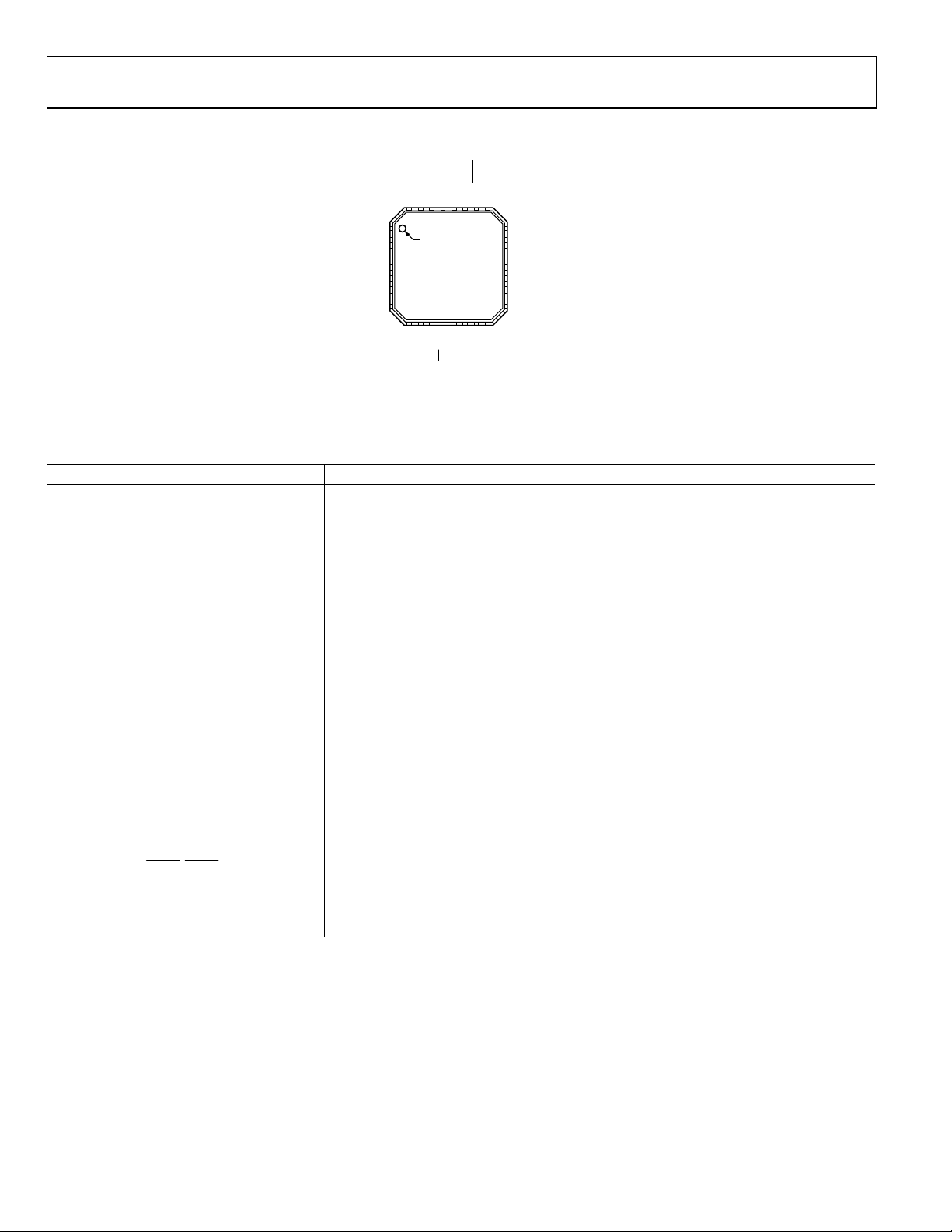
PIN CONFIGURATION AND FUNCTION DESCRIPTIONS
VDD
OUT1
OUT1
Y1
Y0
Y3
Y2
31
30
32
GND
29
28
27
26
25
1Y4
PIN 1
2Y5
INDICATOR
3A0
4A1
AD9552
5A2
TOP VIEW
6RESET
(Not to Scale)
7VDD
8LDO
9
11
10
12
13
CS
REF
XTAL
XTAL
NOTES
1. EXPOSE D DIE PAD MUST BE
CONNECTED TO GND.
SCLK
24 GND
23 O UT2
22
OUT2
21 V DD
20 L OCKED
19 L DO
18 V DD
17 L DO
14
15
16
SDIO
FILTER
OUTSEL
07806-002
Figure 2. Pin Configuration
Table 8. Pin Function Descriptions
Pin No. Mnemonic Type1 Description
29, 30, 31,
32, 1, 2
Y0, Y1, Y2, Y3, Y4,
Y5
I
Control Pins. These pins select preset values for the PLL feedback divider and the OUT1
dividers based on the input reference frequency selected via the A[0:2] pins and have
internal 100 kΩ pull-up resistors.
3, 4, 5 A0, A1, A2 I
Control Pins. These pins select the input reference frequency and have internal 100 kΩ pullup resistors.
6 RESET I
Digital Input, Active High. Resets internal logic to default states. This pin has an internal
100 kΩ pull-up resistor, so the default state of the device is reset.
7, 18, 21, 28 VDD P Power Supply Connection: 3.3 V Analog Supply.
8, 17, 19 LDO P/O
LDO Decoupling Pins. Connect a 0.47 F decoupling capacitor from each of these pins to
ground.
9, 10 XTAL I Crystal Resonator Input. Connect a crystal resonator across these pins.2
11 REF I
Reference Clock Input. Connect this pin to an active clock input signal, or connect it to VDD
when using a crystal resonator across the XTAL pins.
12
CS
I Digital Input, Active Low, Chip Select.
13 SCLK I Serial Data Clock.
14 SDIO I/O Digital Serial Data Input/Output.
15 OUTSEL I
Logic 0 selects LVDS and Logic 1 selects LVPECL-compatible levels for both OUT1 and OUT2
when the outputs are not under SPI port control. Can be overridden via the programming
registers. This pin has an internal 100 kΩ pull-up resistor.
16 FILTER I/O Loop Filter Node for the PLL. Connect an external 12 nF capacitor from this pin to Pin 17 (LDO).
20 LOCKED O Active High Locked Status Indicator for the PLL.
26, 22
OUT1
, OUT2
O Complementary Square Wave Clocking Outputs.
27, 23 OUT1, OUT2 O Square Wave Clocking Outputs.
24, 25 GND P Analog Ground.
EP Exposed Die Pad The exposed die pad must be connected to GND.
1
I = input, I/O = input/output, O = output, P = power, P/O = power/output.
2
When no crystal is in use, leave these pins floating. The terminations are handled by internal circuitry.
Rev. D | Page 8 of 32
AD9552
m
m
m
m
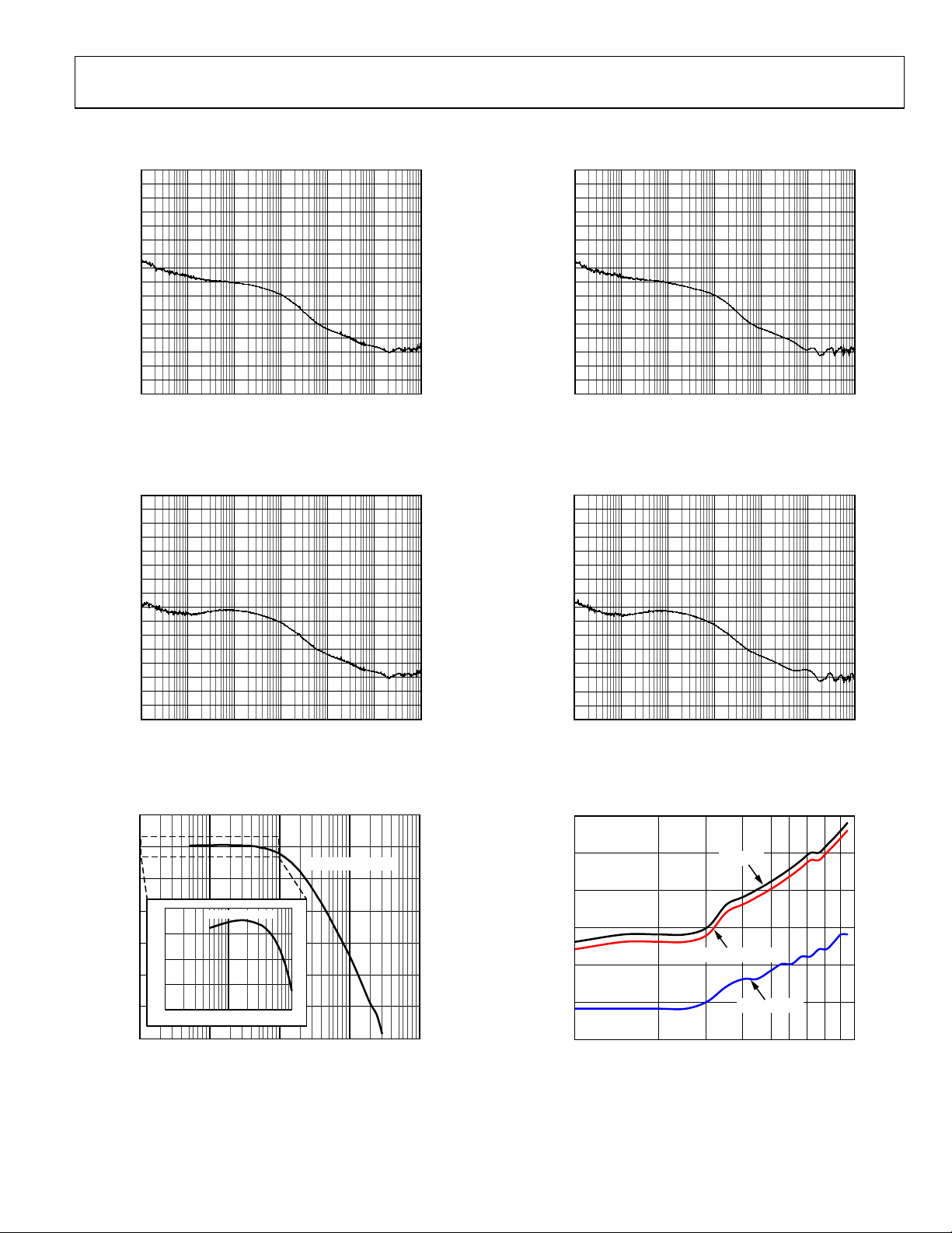
TYPICAL PERFORMANCE CHARACTERISTICS
–20
–30
–40
–50
–60
–70
–80
–90
–100
–110
–120
PHASE NOISE (dB)
–130
–140
–150
–160
–170
–180
100 1k 10k 100k 1M 10M 100M
CARRIER 624.988784MHz 0.4009dB
FREQUENCY (Hz)
Figure 3. Phase Noise, Fractional-N, Pin Programmed
= 19.44 MHz, f
(f
XTAL
= 625 MHz)
OUT1
–20
–30
–40
–50
–60
–70
–80
–90
–100
–110
–120
PHASE NOISE (dB)
–130
–140
–150
–160
–170
–180
100 1k 10k 100k 1M 10M 100M
07806-014
Figure 6. Phase Noise, Integer, SDM Off
(f
XTAL
CARRIER 622.068199MHz 0.5831dB
FREQUENCY (Hz)
= 19.44 MHz, f
= 622.08 MHz)
OUT1
07806-016
–20
–30
–40
–50
–60
–70
–80
–90
–100
–110
–120
PHASE NOISE (dB)
–130
–140
–150
–160
–170
–180
100 1k 10k 100k 1M 10M 100M
CARRIER 624.999995MHz 0.4057dB
FREQUENCY (Hz)
Figure 4. Phase Noise, Fractional-N, Pin Programmed
= 19.44 MHz, f
(f
REF
10
0
–10
1
–20
0
–30
–1
–40
JITTER T RANSFER (dB)
–2
–50
–3
–60
1k 10k 100k 1M 10M
JITTER PEAKI NG
1k 10k 100k
FREQUENCY OFFSET (Hz)
= 625 MHz)
OUT1
JITTER T RANSFER
Figure 5. Jitter Transfer and Jitter Peaking
–20
–30
–40
–50
–60
–70
–80
–90
–100
–110
–120
PHASE NOISE (dB)
–130
–140
–150
–160
–170
–180
100 1k 10k 100k 1M 10M 100M
07806-015
CARRIER 622.079986MHz 0.3798dB
FREQUENCY (Hz )
07806-017
Figure 7. Phase Noise, Integer, SDM Off
= 19.44 MHz, f
(f
REF
35
30
25
20
15
SUPPLY CURRENT (mA)
10
5
07806-018
100 1k
FREQUENCY (MHz)
= 622.08 MHz)
OUT1
LVPECL
LVDS (STRONG)
LVDS (WEAK)
07806-019
Figure 8. Supply Current vs. Output Frequency,
LVPECL and LVDS (15 pF Load)
Rev. D | Page 9 of 32
AD9552
V
25
20
15
10
SUPPLY CURRENT (mA)
5
0
0 50 100 150 200 250
FREQUENCY (MHz )
Figure 9. Supply Current vs. Output Frequency,
CMOS (15 pF Load)
4.0
3.5
3.0
2.5
2.0
20pF
10pF
5pF
07806-020
1.6
1.4
1.2
1.0
0.8
AMPLITUDE (V p-p)
0.6
0.4
0 200 400 600 800 1000
LVPECL
LVDS (STRONG)
LVDS (WEAK)
FREQUENCY (MHz )
Figure 12. Peak-to-Peak Output Voltage vs. Frequency,
LVPECL and LVDS (15 pF Load)
60
55
07806-023
1.5
AMPLITUDE (V p-p)
1.0
0.5
0
0 100 2 00 300 400 500
FREQUENCY (MHz)
Figure 10. Peak-to-Peak Output Voltage vs. Frequency,
CMOS
55
54
53
52
DUTY CYCL E (%)
51
50
0 100 200 300
FREQUENCY (MHz )
5pF
10pF
20pF
Figure 11. Duty Cycle vs. Output Frequency, CMOS
DUTY CYCLE (%)
LVDS (WEAK)
LVDS (STRONG)
LVPECL
50
07806-021
100 200 300 400 500 600 700 800 900 1000
FREQUENCY (MHz)
07806-024
Figure 13. Duty Cycle vs. Output Frequency,
LVPECL and LVDS (15 pF Load)
200mV/DI
500ps/DIV
07806-022
07806-025
Figure 14. Typical Output Waveform, LVPECL (805 MHz)
Rev. D | Page 10 of 32

AD9552
V
V
100mV/DI
500ps/DIV
Figure 15. Typical Output Waveform, LVDS
(805 MHz, 3.5 mA Drive Current)
500mV/DI
07806-026
1.25ns/DI V
07806-027
Figure 16. Typical Output Waveform, CMOS
(250 MHz, 15 pF Load)
Rev. D | Page 11 of 32
AD9552
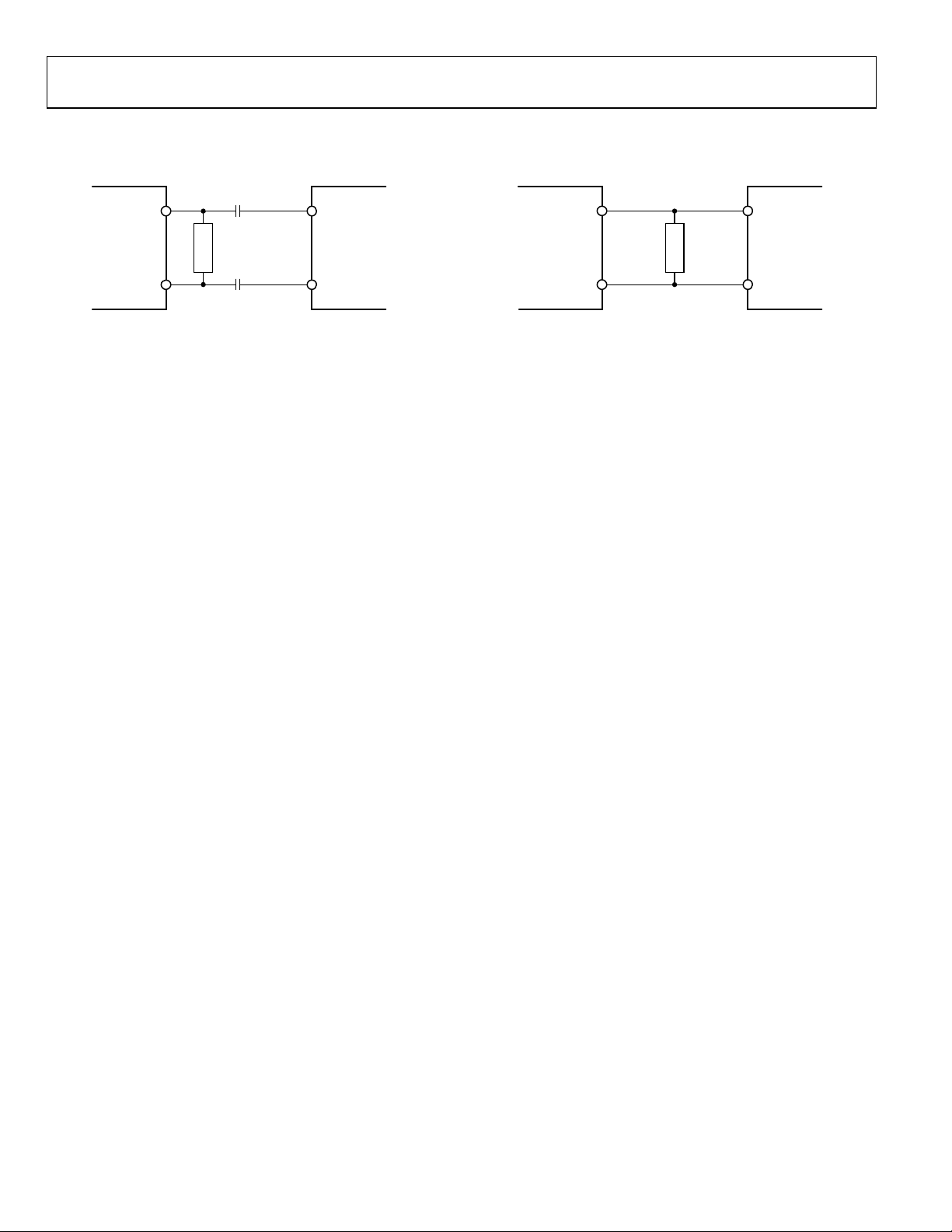
INPUT/OUTPUT TERMINATION RECOMMENDATIONS
0.1µF
AD9552
3.3V
DIFFERENTIAL
OUTPUT
(LVDS OR
LVPECL MO DE)
100Ω
IMPEDANCE
0.1µF
HIGH
INPUT
DOWNSTREAM
DEVICE
AD9552
3.3V
DIFFERENTIAL
OUTPUT
(LVDS OR
LVPECL MODE )
DOWNSTREAM
100Ω
DEVICE
Figure 17. AC-Coupled LVDS or LVPECL Output Driver
07806-028
07806-029
Figure 18. DC-Coupled LVDS or LVPECL Output Driver
Rev. D | Page 12 of 32
AD9552
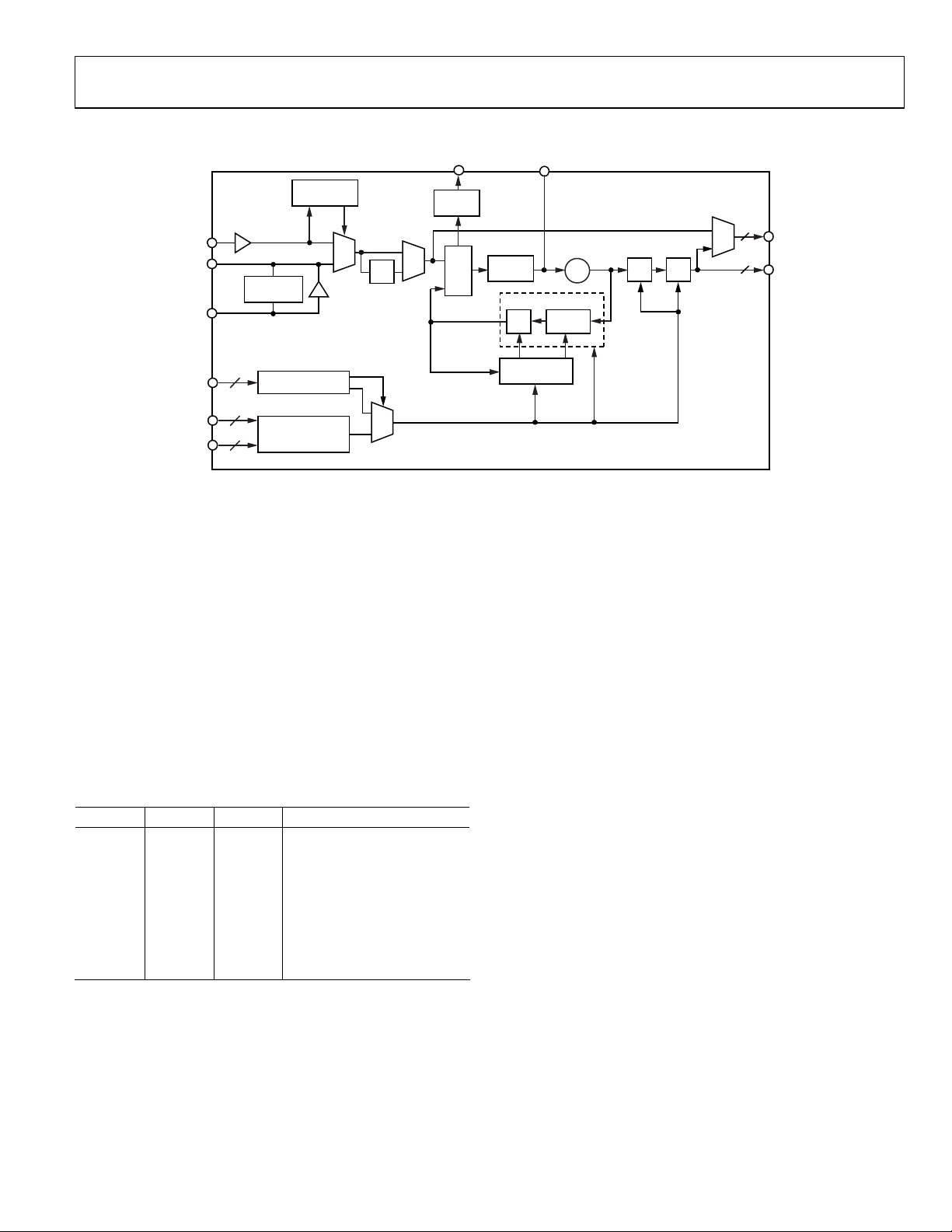
THEORY OF OPERATION
LOCKED
DETECTOR
REFA
XTAL
XTAL
SERIAL
PORT
A2:0
Y5:0
TUNING
CONTROL
3
REGISTER BANK
3
PRECONFIGURED
6
DIVIDER VALUES
2×
PRESET FREQUENCY RATIOS
The frequency selection pins (A[2:0] and Y[5:0]) allow the user
to hardwire the device for preset input and output divider values
based on the pin logic states (see Figure 19). The pins decode
ground or open connections as Logic 0 or Logic 1, respectively.
Use the serial I/O port to change the divider values from the
preset values provided by the A[2:0] and Y[5:0] pins.
The A[2:0] pins select one of eight input reference frequencies
(see Tabl e 9). The user supplies the input reference frequency by
connecting a single-ended clock signal to the REF pin or a crystal
resonator across the XTAL pins. If the A[2:0] pins select 10 MHz,
12 MHz, 12.8 MHz, or 16 MHz, the input frequency to the AD9552
doubles internally. Alternatively, if Register 0x1D[2] is set to 1,
the input frequency doubles.
Table 9. Input Reference Frequency Selection Pins
A2 A1 A0 Reference Frequency (MHz)
0 0 0 10.00
0 0 1 12.00
0 1 0 12.80
0 1 1 16.00
1 0 0 19.20
1 0 1 19.44
1 1 0 20.00
1 1 1 26.00
LOCK
DETECT
PFD
N, MOD, FRAC, P0, P
Figure 19. Detailed Block Diagram
FILTER
AD9552
2
OUT2
2
OUT1
07806-006
CHARGE
PUMP
N
1
MODULATOR
MOD,
FRAC
1
3350MHz TO
4050MHz
N = 4N1 + N
4 OR 5
Σ-∆
VCO
4TO11 1TO 63
P
P
0
1
0
N
P0, P
1
The Y[5:0] pins select the appropriate feedback and output dividers
to synthesize the output frequencies (see Tabl e 1 0 ). The output
frequencies provided in Ta bl e 10 are exact; that is, the number of
decimal places displayed is sufficient to maintain full precision.
Where a decimal representation is not practical, a fractional
multiplier is used.
The VCO and output frequency shift in frequency by a ratio of the
reference frequency used vs. the frequency specified in Tabl e 9.
Note that the VCO frequency must stay within the minimum and
maximum range specified in Ta ble 1 . Typically, the selection of
the VCO frequency band, as well as the gain adjustment, by the
external pin strap occurs as part of the device’s automatic VCO
calibration process, which initiates at power up (or reset). If the
user changes the VCO frequency band via the SPI interface,
however, a forced VCO calibration should be initiated by first
enabling SPI control of the VCO calibration (Register 0x0E[2] = 1)
and then writing a 1 to the calibrate VCO bit (Register 0x0E[7]).
Rev. D | Page 13 of 32

AD9552
Table 10. Output Frequency Selection Pins
Y5 Y4 Y3 Y2 Y1 Y0 VCO Frequency (MHz) Output (MHz)
0 0 0 0 0 0 3732.48 51.84
0 0 0 0 0 1 3888 54
0 0 0 0 1 0 3840 60
0 0 0 0 1 1 3932.16 61.44
0 0 0 1 0 0 3750 62.5
0 0 0 1 0 1 3733.296 66.666
0 0 0 1 1 0 3560.439 74.17582
0 0 0 1 1 1 3564 74.25
0 0 1 0 0 0 3732.48 77.76
0 0 1 0 0 1 3932.16 98.304
0 0 1 0 1 0 4000 100
0 0 1 0 1 1 3825 106.25
0 0 1 1 0 0 3840 120
0 0 1 1 0 1 4000 125
0 0 1 1 1 0 3724 133
0 0 1 1 1 1 3732.48 155.52
0 1 0 0 0 0 3750 156.25
0 1 0 0 0 1 3825 159.375
0 1 0 0 1 0 3867.188 161.1328125
0 1 0 0 1 1 3944.531 10518.75/64
0 1 0 1 0 0 3999.086 155.52 × (15/14)
0 1 0 1 0 1 4015.959 155.52 × (255/237)
0 1 0 1 1 0 4023.878 167.6616
0 1 0 1 1 1 3554.742 177.7371
0 1 1 0 0 0 3932.16 245.76
0 1 1 0 0 1 4000 250
0 1 1 0 1 0 3732.48 311.04
0 1 1 0 1 1 3840 320
0 1 1 1 0 0 4000 400
0 1 1 1 0 1 3471.4 433.925
0 1 1 1 1 0 3718.75 531.25
0 1 1 1 1 1 3763.2 537.6
1 0 0 0 0 0 3984.375 569.1964
1 0 0 0 0 1 3732.48 622.08
1 0 0 0 1 0 3748.229 624.7048
1 0 0 0 1 1 3750 625
1 0 0 1 0 0 3763.978 622.08 × (239/237)
1 0 0 1 0 1 3779.927 629.9878
1 0 0 1 1 0 3840 640
1 0 0 1 1 1 3849.12 641.52
1 0 1 0 0 0 3867.188 625 × (66/64)
1 0 1 0 0 1 3944.531 657.421875
1 0 1 0 1 0 3961.105 657.421875 × (239/238)
1 0 1 0 1 1 3999.086 622.08 × (15/14)
1 0 1 1 0 0 4014.769 669.1281
1 0 1 1 0 1 4015.959 622.08 × (255/237)
1 0 1 1 1 0 4017.857 625 × (15/14)
1 0 1 1 1 1 4025.032 670.8386
1 1 0 0 0 0 4032.976 622.08 × (255/236)
1 1 0 0 0 1 3452.846 625 × (66/64) × (15/14)
1 1 0 0 1 0 3467.415 625 × (255/237) × (66/64)
1 1 0 0 1 1 3468.75 693.75
1 1 0 1 0 0 3481.996 622.08 × (253/226)
1 1 0 1 0 1 3521.903 657.421875 × (255/238)
Rev. D | Page 14 of 32

AD9552
Y5 Y4 Y3 Y2 Y1 Y0 VCO Frequency (MHz) Output (MHz)
1 1 0 1 1 0 3536.763 657.421875 × (255/237)
1 1 0 1 1 1 3582.686 716.5372
1 1 1 0 0 0 3593.75
1 1 1 0 0 1 3598.672
1 1 1 0 1 0 3740.355
1 1 1 0 1 1 3750
1 1 1 1 0 0 3888
1 1 1 1 0 1 3897.843
1 1 1 1 1 0 3906.25
1 1 1 1 1 1 4028.32 625 × (10/8) × (66/64)
718.75
719.7344
748.0709
750
777.6
779.5686
781.25
COMPONENT BLOCKS
Input Reference
The AD9552 offers the following input reference options:
• Crystal resonator connected directly across the XTAL pins
• CMOS-compatible, single-ended clock source connected
directly to the REF pin
In the case of a crystal resonator, the AD9552 expects a crystal
with a specified load capacitance of 15 pF (default). The
AD9552 provides the load capacitance internally. The internal
load capacitance consists of a fixed component of 13 pF and a
variable (programmable) component of 0 pF to 15.75 pF.
After applying power to the AD9552 (or after a device reset),
the programmable component assumes a value of 2 pF. This
establishes the default load capacitance of 15 pF.
To accommodate crystals with a specified load capacitance other
than 15 pF (8 pF to 23.75 pF), the user can adjust the programmable capacitance in 0.25 pF increments via Register 0x1B[5:0].
Note that when the user sets Register 0x1B[7] to 0 (enabling SPI
control of the XTAL tuning capacitors), the variable capacitance
changes from 2 pF (its power-up value) to 15.75 pF due to the
default value of Register 0x1B[5:0]. This causes the crystal load
capacitance to be 23.75 pF until the user overwrites the default
contents of Register 0x1B[5:0].
A noncomprehensive, alphabetical list of crystal manufacturers
includes the following:
• AV X /Ky o c er a
• ECS
• Epson Toyocom
• Fox Electronics
• NDK
• Siward
The AD9552 evaluation board functions with the NDK
NX3225SA crystal or with the Siward 571200-A258-001 crystal.
Although these crystals meet the load capacitance and motional
resistance requirements of the AD9552 according to their data
sheets, Analog Devices, Inc., does not guarantee their operation
with the AD9552, nor does Analog Devices endorse one supplier
of crystals over another.
Reference Monitor
The REF input includes a monitor circuit that detects signal
presence at the REF input. If the device detects a clock signal on
the REF pin, it automatically selects the REF input as the input
reference source and shuts down the crystal oscillator. This automatic preference for a REF input signal is the default mode of
operation. However, the user can override the default setting via
Register 0x1D[0]. Setting this bit forces the device to override the
signal detector associated with the REF input and activates the
crystal oscillator (whether or not a REF input signal is present).
2× Frequency Multiplier
The 2× frequency multiplier provides the option to double
the frequency delivered by either the REF or XTAL input. This
allows the user to take advantage of a higher frequency delivered to the PLL, which allows for greater separation between
the frequency generated by the PLL and the associated reference
spur. However, increased reference spur separation comes at the
expense of the harmonic spurs introduced by the frequency
multiplier. As such, beneficial use of the frequency multiplier
is application specific.
PLL
The PLL consists of a phase/frequency detector (PFD), a
partially integrated analog loop filter (see Figure 20), an
integrated voltage-controlled oscillator (VCO), and a
feedback divider with an optional third-order SDM that
allows for fractional divide ratios. The PLL produces a
nominal 3.7 GHz signal that is phase-locked to the input
reference signal.
The loop bandwidth of the PLL is nominally 50 kHz. The PFD of
the PLL drives a charge pump that automatically changes current
proportionately to the feedback divider value. This increase or
decrease in current maintains a constant loop bandwidth with
changes in the input reference or the output frequency.
FROM
CHARGE
PUMP
2.5kΩ
16
EXTERNAL
LOOP FILTER
CAPACITOR
1.25kΩ 1.25kΩ 2.5kΩ
105pF 15pF 15pF 20pF
Figure 20. Internal Loop Filter
TO
VCO
07806-004
Rev. D | Page 15 of 32

AD9552
The gain of the PLL is proportional to the current delivered
by the charge pump. The user can override the default charge
pump current setting, and, thereby, the PLL gain, by using
Register 0x0A[7:0].
The PLL has a VCO with 128 frequency bands spanning a range
of 3350 MHz to 4050 MHz (3700 MHz nominal). However, the
actual operating frequency within a particular band depends on
the control voltage that appears on the loop filter capacitor. The
control voltage causes the VCO output frequency to vary linearly
within the selected band. This frequency variability allows the
control loop of the PLL to synchronize the VCO output signal
with the reference signal applied to the PFD. Typically, selection
of the VCO frequency band (as well as gain adjustment) occurs
automatically as part of the device’s automatic VCO calibration
process, which initiates at power up (or reset). Alternatively, the
user can force VCO calibration by first enabling SPI control of
VCO calibration (Register 0x0E[2] = 1) and then writing a 1 to
the calibrate VCO bit (Register 0x0E[7]). To facilitate system
debugging, the user can override the VCO band setting by first
enabling SPI control of VCO band (Register 0x0E[0] = 1) and
then writing the desired value to Register 0x10[7:1].
The PLL has a feedback divider coupled with a third-order
SDM that enables the PLL to provide integer-plus-fractional
frequency upconversion. The integer factor, N, is variable via
an 8-bit programming register. The range of N is from N
255, where N
is 36 or 47 depending on whether the SDM is
MIN
disabled or enabled, respectively. The SDM in the feedback path
allows for a fractional divide value that takes the form of N +
F/M, where N is the integer part (eight bits), M is the modulus
(20 bits), and F is the fractional part (20 bits), with all three
parameters being positive integers.
The feedback SDM gives the AD9552 the ability to support a
wide range of output frequencies with exact frequency ratios
relative to the input reference.
PLL Locked Indicator
The PLL provides a status indicator that appears at an external
pin (LOCKED). The indicator shows when the PLL has acquired
a locked condition.
Output Dividers
Two integer dividers exist in the output chain. The first divider (P0)
yields an integer submultiple of the VCO frequency. The second
divider (P
submultiple of the output frequency of the P
) establishes the frequency at OUT1 as an integer
1
divider.
0
Input-to-OUT2 Option
By default, OUT2 delivers an output frequency that is the same
frequency as OUT1. However, the user has the option of making
OUT2 a replica of the input frequency (REF or XTAL) by
programming Register 33[3] = 1.
MIN
to
Output Drivers
The user has control over the following output driver parameters
via the programming registers:
• Logic family and pin functionality
• Polarity (for CMOS family only)
• Drive current
• Power-down
The logic families are LVDS, LVPECL, and CMOS. Selection of
the logic family is via the mode control bits in the OUT1 driver
control register (Register 0x32[5:3]) and the OUT2 driver control
register (Register 0x34[5:3]), as detailed in Tab l e 1 1 . Regardless
of the selected logic family, each output driver uses two pins:
OUT1 and
OUT1
are used by one driver, and OUT2 and
OUT2
are used by the other. This enables support of the differential
signals associated with the LVDS and LVPECL logic families.
CMOS, on the other hand, is a single-ended signal requiring
only one output pin, but both output pins are available for
optional provision of a dual, single-ended CMOS output clock.
Refer to the first entry (CMOS (both pins)) in . Tab l e 1 1
Table 11. Output Channel Logic Family and Pin Functionality
Mode
Control Bits[2:0]
000 CMOS (both pins)
001 CMOS (positive pin), tristate (negative pin)
010 Tristate (positive pin), CMOS (negative pin)
011 Tristate (both pins)
100 LVDS
101 LVPECL
110 Undefined
111 Undefined
Logic Family and Pin Functionality
If the mode bits indicate the CMOS logic family, the user has
control of the logic polarity associated with each CMOS output
pin via the OUT1 and OUT2 driver control registers.
If the mode bits indicate the CMOS or LVDS logic family, the
user can select whether the output driver uses weak or strong
drive capability via the OUT1 and OUT2 driver control registers.
In the case of the CMOS family, the strong setting allows for
driving increased capacitive loads. In the case of the LVDS
family, the nominal weak and strong drive currents are 3.5 mA
and 7 mA, respectively.
The OUT1 and OUT2 driver control registers also have a powerdown bit to enable/disable the output drivers. The power-down
function is independent of the logic family selection.
Note that, unless the user programs the device to allow SPI port
control of the output drivers, the drivers default to LVPECL or
LVDS, depending on the logic level on the OUTSEL pin (Pin 15).
For OUTSEL = 0, both outputs are LVDS. For OUTSEL = 1, both
outputs are LVPECL. In the pin-selected LVDS mode, the user
can still control the drive strength, using the SPI port.
Rev. D | Page 16 of 32

AD9552
{
}
{
}
{
}
{
}
{
}
{
}
{
}
PART INITIALIZATION AND AUTOMATIC POWERON RESET
The AD9552 has an internal power-on reset circuit. At power-up,
internal logic relies on the internal reference monitor to select
either the crystal oscillator or the reference input and then
initiates VCO calibration using whichever is found. If both are
present, the external reference path is chosen.
VCO calibration is required in order for the device to lock. If
the input reference signal is not present, VCO calibration waits
until a valid input reference is present. As soon as an input
reference signal is present, VCO calibration starts. The user
should wait at least 3 ms for the VCO calibration routine to
finish before programming the VCO control register (Register
0x0E) via serial communication.
If the user wishes to use the crystal oscillator input even if the
reference input is present, the user needs to set Bit 0 (use crystal
resonator) in Register 0x1D.
Any change to the preset frequency selection pins or the PLL
divide ratios requires the user to recalibrate the VCO.
OUTPUT/INPUT FREQUENCY RELATIONSHIP
The frequency at OUT1 and OUT2 is a function of the PLL
feedback divider values (N, FRAC, and MOD) and the output
divider values (P
frequency at OUT1 and OUT2 (f
are as follows.
OUT
f
= f
OUT2
where:
f
is the input reference or crystal resonator frequency.
REF
K is the input mode scale factor.
N is the integer feedback divider value.
FRAC and MOD are the fractional feedback divider values.
P
and P1 are the OUT1 divider values.
0
The numerator of the f
factor, which has an integer part (N) due to an integer divider
along with an optional fractional part (FRAC/MOD) associated
with the feedback SDM.
The following constraints apply:
N
MIN
and P1). The equations that define the
0
and f
OUT1
FRAC
1
OUT1
2,1∈K
⎜
⎝
OUT1
47,36∈
NNN
MINMIN
11,,5,40L∈P
63,,2,11L∈P
⎛
N
⎜
Kff
×=
REF
⎞
+
MOD
⎟
⎟
PP
10
⎠
equation contains the feedback division
255,,1, L+∈
575,048,1,,1,0 L∈FRAC
575,048,1,,2,1 L∈MOD
, respectively)
OUT2
Note that N
of N
MIN
SDM is disabled or N
depends on the 2× frequency multiplier. K = 1 when the 2×
frequency multiplier is bypassed, or K = 2 when it is enabled.
The frequency at the input to the PFD (f
follows:
f
PFD
The operating range of the VCO (3.35 GHz ≤ f
places the following constraint on f
⎛
⎜
⎜
⎝
CALCULATING DIVIDER VALUES
This section provides a three-step procedure for calculating the
divider values when given a specific f
frequency of either the REF input signal source or the external
crystal resonator). The computation process is described in
general terms, but a specific example is provided for clarity.
The example is based on a frequency control pin setting of
A[2:0] = 111 (see Table 9) and Y[5:0] = 101000 (see Tab l e 1 0 ),
yielding the following:
f
REF
f
OUT1
1. Determine the output divide factor (ODF).
Note that the VCO frequency (f
4050 MHz. The ratio, f
Given the specified value of f
range of f
must be an integer, which means that ODF = 6 (because 6
is the only integer between 5.2 and 6.3).
2. Determine suitable values for P
The ODF is the product of the two output dividers, so
ODF = P
for the given example. Therefore, P
that P
the Output/Input Frequency Relationship section). These
constraints lead to the single solution: P
Although this particular example yields a single solution
for the output divider values with f
f
OUT1
one. For example, if f
34 to 40. This leads to an assortment of possible values for
P0 and P1, as shown in Tabl e 12 .
and K can each be one of two values. The value
MIN
depends on the state of the SDM. N
= 47 when it is enabled. The value of K
MIN
= K × f
3350
N
+
FRAC
MOD
REF
⎞
⎟
⎟
⎠
MHz
:
PFD
⎛
4050
⎜
f
≤≤
PFD
⎜
N
⎝
FRAC
+
MOD
OUT1/fREF
= 36 when the
MIN
) is calculated as
PFD
≤ 4.05 GHz)
VCO
⎞
⎟
MHz
⎟
⎠
ratio (f
REF
is the
= 26 MHz
= 625 × (66/64) MHz
) spans 3350 MHz to
VCO
VCO/fOUT1
, the ODF spans a range of 5.2 to 6.3. The ODF
VCO
. It has already been determined that ODF = 6
0P1
and P1 are both integers and that 4 ≤ P0 ≤ 11 (see
0
, indicates the required ODF.
(~644.53 MHz) and the
OUT1
and P1.
0
= 6 with the constraints
0P1
= 6 and P1 = 1.
0
≈ 644.53 MHz, some
OUT1
frequencies result in multiple ODFs rather than just
= 100 MHz the ODF ranges from
OUT1
Rev. D | Page 17 of 32

AD9552
N
Table 12. Combinations for P0 and P1
P0 P
4 9 36
4 10 40
5 7
5 8
6 6 36
7 5
8 5
9 4
10 4 40
The P0 and P1 combinations listed in Tab le 1 2 are all equally
valid. However, note that they yield only three valid ODF
values (35, 36, and 40) from the original range of 34 to 40.
3. Determine the feedback divider values for the PLL.
Repeat this step for each ODF when multiple ODFs exist
(for example, 35, 36, and 40 in the case of Tab l e 1 2 ).
To calculate the feedback divider values for a given ODF,
use the following equation:
⎛
f
⎜
⎜
⎝
Note that the left side of the equation contains variables with
known quantities. Furthermore, the values are necessarily
rational, so the left side is expressible as a ratio of two integers, X and Y. Following is an example equation.
⎛
625
⎜
⎜
⎜
⎜
⎝
In the context of the AD9552, X/Y is always an improper
fraction. Therefore, it is expressible as the sum of an integer,
N, and the proper fraction, R/Y (R and Y are integers).
X
Y
1664
This particular example yields N = 148, Y = 1664, and
R = 1228. To arrive at this result, use long division to convert
the improper fraction, X/Y, to an integer (N) and a proper
fraction (R/Y). Note that dividing Y into X by means of
long division yields an integer, N, and a remainder, R. The
proper fraction has a numerator (R, the remainder) and a
denominator (Y, the divisor), as shown in Figure 21.
ODF (P0 × P1)
1
⎞
1
OUT
⎟
⎟
f
REF
⎠
66
⎤
⎡
⎥
⎢
64
⎦
⎣
26
N
+=
500,247
=×
ODF
⎞
⎟
⎟
6
⎟
⎟
⎠
R
Y
R
N +=
Y
YX
–NY
R
Figure 21. Example Long Division
35
40
35
40
36
X
Y
)6)(66(625
)64(26
X
= N +
Y
1664
R
Y
X
500,247
===×
Y
07806-005
It is imperative that long division be used to obtain the correct
results. Avoid the use of a calculator or math program, because
these do not always yield correct results due to internal rounding
and/or truncation. Some calculators or math programs may be up
to the task if they can handle very large integer operations, but such
are not common.
In the example, N = 148 and R/Y = 1228/1664, which reduces
to R/Y = 307/416. These values of N, R, and Y constitute the
following respective feedback divider values:
N = 148, FRAC = 307, and MOD = 416.
The only caveat is that N and MOD must meet the constraints
given in the Output/Input Frequency Relationship section.
In the example, FRAC is nonzero, so the division value is an
integer plus the fractional component, FRAC/MOD. This
implies that the feedback SDM is necessary as part of the
feedback divider. If FRAC = 0, the feedback division factor
is an integer and the SDM is not required (it can be bypassed).
Although the feedback divider values obtained in this way
provide the proper feedback divide ratio to synthesize the exact
output frequency, they may not yield optimal jitter performance
at the final output. One reason for this is that the value of MOD
defines the period of the SDM, which has a direct impact on the
spurious output of the SDM. Specifically, in the spectral band
from dc to f
, the SDM exhibits spurs at intervals of f
PFD
PFD
/
MOD. Thus, the spectral separation (f) of the spurs associated
with the feedback SDM is
f
PFD
MOD
f
=Δ
Because the SDM is in the feedback path of the PLL, these spurs
appear in the output signal as spurious components offset by f
from f
large spurs with relatively large frequency offsets from f
. Therefore, a small MOD value pro-duces relatively
OUT1
OUT1
,
whereas a large MOD value produces smaller spurs but more
closely spaced to f
. Clearly, the value of MOD has a direct
OUT1
impact on the spurious content (that is, jitter) at OUT1.
Generally, the largest possible MOD value yields the smallest spurs.
Thus, it is desirable to scale MOD and FRAC by the integer part
20
divided by the value of MOD obtained previously. In the
of 2
example, the value of MOD is 416, yield-ing a scale factor of 2520
(the integer part of 220/416). A scale factor of 2520 leads to FRAC
= 307 × 2520 = 773,640 and MOD = 416 × 2520 = 1,048,320.
LOW DROPOUT (LDO) REGULATORS
The AD9552 is powered from a single 3.3 V supply and contains
on-chip LDO regulators for each function to eliminate the need
for external LDOs. To ensure optimal performance, each LDO
output should have a 0.47 F capacitor connected between its
access pin and ground, and this capacitor should be kept as
close to the device as possible.
Rev. D | Page 18 of 32

AD9552
APPLICATIONS INFORMATION
THERMAL PERFORMANCE
Table 13. Thermal Parameters for the 32-Lead LFCSP Package
Symbol Thermal Characteristic Using a JEDEC51-7 Plus JEDEC51-5 2S2P Test Board1 Value2 Unit
θJA Junction-to-ambient thermal resistance, 0.0 m/sec airflow per JEDEC JESD51-2 (still air) 40.5 °C/W
θ
Junction-to-ambient thermal resistance, 1.0 m/sec airflow per JEDEC JESD51-6 (moving air) 35.4 °C/W
JMA
θ
Junction-to-ambient thermal resistance, 2.5 m/sec airflow per JEDEC JESD51-6 (moving air) 31.8 °C/W
JMA
θJB Junction-to-board thermal resistance, 1.0 m/sec airflow per JEDEC JESD51-8 (moving air) 23.3 °C/W
θJC Junction-to-case thermal resistance (die-to-heat sink) per MIL-Std 883, Method 1012.1 4.2 °C/W
ΨJT Junction-to-top-of-package characterization parameter, 0 m/sec airflow per JEDEC JESD51-2 (still air) 0.4 °C/W
1
The exposed pad on the bottom of the package must be soldered to ground to achieve the specified thermal performance.
2
Results are from simulations. The PCB is a JEDEC multilayer type. Thermal performance for actual applications requires careful inspection of the conditions in the
application to determine whether they are similar to those assumed in these calculations.
The AD9552 is specified for an ambient temperature (T
ensure that T
is not exceeded, an airflow source can be used.
A
). To
A
Use the following equation to determine the junction temperature on the application PCB:
= T
J
+ (ΨJT × PD)
CASE
T
where:
is the junction temperature (°C).
T
J
is the case temperature (°C) measured by the customer
T
CASE
at the top center of the package.
is the value indicated in Tab l e 1 3 .
Ψ
JT
P
is the power dissipation (see the Specifications section).
D
Val u es of θ
considerations. θ
of T
where T
Val u es of θ
are provided for package comparison and PCB design
JA
can be used for a first-order approximation
JA
using the following equation:
J
T
= TA + (θJA × PD)
J
is the ambient temperature (°C).
A
are provided for package comparison and PCB
JC
design considerations when an external heat sink is required.
Val u es of θ
are provided for package comparison and PCB
JB
design considerations.
Rev. D | Page 19 of 32
AD9552
SERIAL CONTROL PORT
The AD9552 serial control port is a flexible, synchronous, serial
communications port that allows an easy interface to many
industry-standard microcontrollers and microprocessors. Single
or multiple byte transfers are supported, as well as MSB first or
LSB first transfer formats. The AD9552 serial control port is
configured for a single bidirectional I/O pin (SDIO only). Note
that, to enable serial communication with the AD9552, the pin
select pins, A[2:0] (Pin 3, Pin 4, and Pin 5) and Y[5:0] (Pin 29
through Pin 32 and Pin 1 and Pin 2) must all be set to Logic 1.
Each of these pins has an internal 100 k pull-up resistor so
that they can be left floating during serial communication.
The serial control port has two types of registers: read-only and
buffered. Read-only registers are nonbuffered and ignore write
commands. All writable registers are buffered (also referred to
as mirrored) and require an I/O update to transfer the new values
from a temporary buffer on the chip to the actual register. To
invoke an I/O update, write a 1 to the I/O update bit found in
Register 0x05[0]. Because any number of bytes of data can
be changed before issuing an update command, the update
simultaneously enables all register changes occurring since
any previous update.
SERIAL CONTROL PORT PIN DESCRIPTIONS
SCLK (serial data clock) is the serial shift clock. This pin is an
input. SCLK is used to synchronize serial control port reads and
writes. Write data bits are registered on the rising edge of this
clock, and read data bits are registered on the falling edge. This
pin is internally pulled down by a 30 kΩ resistor to ground.
SDIO (digital serial data input/output) is a dual-purpose pin
that acts as input only or as an input/output. The AD9552
defaults to bidirectional pins for I/O.
CS
(chip select bar) is an active low control that gates the read and
write cycles. When
CS
is high, SDIO is in a high impedance state.
This pin is internally pulled up by a 100 kΩ resistor to 3.3 V. It
should not be left floating. See the
section on the use of the
Port
SCLK
SDIO
CS
Figure 22. Serial Control Port
Operation of the Serial Control
CS
pin in a communication cycle.
13
AD9552
14
SERIAL
CONTROL
PORT
12
07806-006
OPERATION OF THE SERIAL CONTROL PORT
Framing a Communication Cycle with CS
The CS line gates the communication cycle (a write or a read oper-
CS
ation).
The
or fewer bytes of data (plus instruction data) are transferred.
Bits[W1:W0] must be set to 00, 01, or 10 (see ). In these
must be brought low to initiate a communication cycle.
CS
stall high function is supported in modes where three
Tabl e 1 4
Rev. D | Page 20 of 32
CS
modes,
may temporarily return high on any byte boundary,
allowing time for the system controller to process the next byte.
CS
can go high on byte boundaries only and can go high during
either part (instruction or data) of the transfer. During this period,
the serial control port state machine enters a wait state until all
data has been sent. If the system controller decides to abort before
the complete transfer of all the data, the state machine must be reset
either by completing the remaining transfer or by returning the
CS
line low for at least one complete SCLK cycle (but fewer than
eight SCLK cycles). A rising edge on the
CS
pin on a nonbyte
boundary terminates the serial transfer and flushes the buffer.
Table 14. Byte Transfer Count
Bytes to Transfer
W1 W0
0 0 1
0 1 2
1 0
1 1 Streaming mode
(Excluding the 2-Byte Instruction)
3
In the streaming mode (Bits[W1:W0] = 11), any number of data
bytes can be transferred in a continuous stream. The register
address is automatically incremented or decremented (see the
CS
MSB/LSB First Transfers section).
must be raised at the end
of the last byte to be transferred, thereby ending the stream mode.
Communication Cycle—Instruction Plus Data
There are two parts to a communication cycle with the AD9552.
The first part writes a 16-bit instruction word into the AD9552,
coincident with the first 16 SCLK rising edges. The instruction
word provides the AD9552 serial control port with information
regarding the data transfer, which is the second part of the
communication cycle. The instruction word defines whether
the upcoming data transfer is a read or a write, the number of
bytes in the data transfer, and the starting register address for
the first byte of the data transfer.
Write
If the instruction word is for a write operation (Bit I15 = 0), the
second part is the transfer of data into the serial control port
buffer of the AD9552. The length of the transfer (1, 2, or 3 bytes;
or streaming mode) is indicated by two bits (Bits[W1:W0]) in
the instruction byte. The length of the transfer indicated by
CS
(Bits[W1:W0]) does not include the 2-byte instruction.
can
be raised after each sequence of eight bits to stall the bus (except
after the last byte, where it ends the cycle). When the bus is stalled,
CS
the serial transfer resumes when
is lowered. Stalling on nonbyte
boundaries resets the serial control port.
Read
If the instruction word is for a read operation (Bit I15 = 1), the
next N × 8 SCLK cycles clock out the data from the address
specified in the instruction word, where N is 1, 2, 3, or 4, as
determined by Bits[W1:W0]. In this case, 4 is used for streaming
AD9552
SCLK
mode, where four or more words are transferred per read. The
data read back is valid on the falling edge of SCLK.
The default mode of the AD9552 serial control port is bidirectional mode, and the data read back appears on the SDIO pin.
By default, a read request reads the register value that is currently
in use by the AD9552. However, setting Register 0x04[0] = 1
causes the buffered registers to be read instead. The buffered
registers are the ones that take effect during the next I/O update.
13
SDIO
CS
Figure 23. Relationship Between the Serial Control Port Register Buffers and
12
CONTROL
PORT
the Control Registers
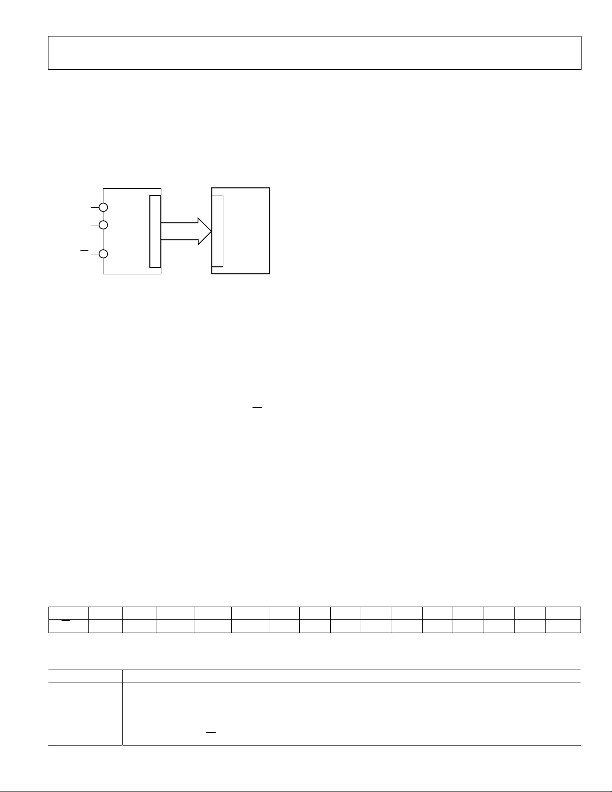
REGISTER
UPDATE
EXECUTE AN
INPUT/OUTPUT
REGISTER BUFFERS
UPDATE
SERIAL
14
AD9552
CONTROL REGI STERS
CORE
07806-007
The AD9552 uses Register 0x00 to Register 0x34. Although the
AD9552 serial control port allows both 8-bit and 16-bit instructions, the 8-bit instruction mode provides access to five address
bits (Address Bits[A4:A0]) only, which restricts its use to Address
Space 0x00 to Address Space 0x01. The AD9552 defaults to 16-bit
instruction mode on power-up, and the 8-bit instruction mode
is not supported.
INSTRUCTION WORD (16 BITS)
The MSB of the instruction word (see Tab l e 1 5 ) is R/W, which
indicates whether the instruction is a read or a write. The next
two bits, W1 and W0, are the transfer length in bytes. The final
13 bits are the address bits (Address Bits[A12:A0]) at which the
read or write operation is to begin.
For a write, the instruction word is followed by the number of
bytes of data indicated by Bits[W1:W0], which is interpreted
according to Ta bl e 14 .
Address Bits[A12:A0] select the address within the register map
that is written to or read from during the data transfer portion
of the communication cycle. The AD9552 uses all of the 13-bit
address space. For multibyte transfers, this address is the starting
byte address.
MSB/LSB FIRST TRANSFERS
The AD9552 instruction word and byte data can be MSB first or
LSB first. The default for the AD9552 is MSB first. The LSB first
mode can be set by writing a 1 to Register 0x00[6] and requires
that an I/O update be executed. Immediately after the LSB first
bit is set, all serial control port operations are changed to LSB
first order.
When MSB first mode is active, the instruction and data bytes
must be written from MSB to LSB. Multibyte data transfers in
MSB first format start with an instruction byte that includes the
register address of the most significant data byte. Subsequent
data bytes must follow in order from high address to low address.
In MSB first mode, the serial control port internal address generator decrements for each data byte of the multibyte transfer cycle.
When LSB first = 1 (LSB first), the instruction and data bytes
must be written from LSB to MSB. Multibyte data transfers
in LSB first format start with an instruction byte that includes
the register address of the least significant data byte followed
by multiple data bytes. The serial control port internal byte
address generator increments for each data byte of the multibyte
transfer cycle.
The AD9552 serial control port register address decrements from
the register address just written toward 0x00 for multibyte I/O
operations if the MSB first mode is active (default). If the LSB
first mode is active, the serial control port register address
increments from the address just written toward 0x34 for
multibyte I/O operations.
Unused addresses are not skipped during multibyte I/O operations.
The user should write the default value to a reserved register and
should write only zeros to unmapped registers. Note that it is more
efficient to issue a new write command than to write the default
value to more than two consecutive reserved (or unmapped)
registers.
Table 15. Serial Control Port, 16-Bit Instruction Word, MSB First
MSB LSB
I15 I14 I13 I12 I11 I10 I9 I8 I7 I6 I5 I4 I3 I2 I1 I0
R/W
W1 W0 A12 A11 A10 A9 A8 A7 A6 A5 A4 A3 A2 A1 A0
Table 16. Definition of Terms Used in Serial Control Port Timing Diagrams
Parameter Description
t
Period of SCLK
CLK
tDV Read data valid time (time from falling edge of SCLK to valid data on SDIO)
tDS Setup time between data and rising edge of SCLK
tDH Hold time between data and rising edge of SCLK
t
S
Setup time between CS
and SCLK
Rev. D | Page 21 of 32

AD9552
SCLK
t
H
t
Minimum period that SCLK should be in a logic high state
HIGH
t
Minimum period that SCLK should be in a logic low state
LOW
CS
DON'T CARE
SCLK
Hold time between CS
and SCLK
DON'T CARE
DON'T CARE
SDIO A12W0W1R/W A11 A10 A9 A8 A7 A6 A5 A4 A3 A2 A1 A0 D7 D6 D5 D4 D3 D2 D1 D0 D7 D6 D5 D4 D3 D2 D1 D0
16-BIT INST RUCTION HEADER REGISTER (N) DATA REGISTE R (N – 1) DATA
Figure 24. Serial Control Port Write—MSB First, 16-Bit Instruction, Two Bytes Data
CS
DON'T CARE DON'T CARE
SDIO
A12W0W1R/W A11 A10 A9 A8 A7 A6 A5 A4 A3 A2 A1 A0
D7 D6 D5 D4 D3 D2 D1 D0 D7 D6 D5 D4 D3 D2 D1 D0 D7 D6 D5 D4 D3 D2 D1 D0 D7 D6 D5 D4 D3 D2 D1 D0
REGISTER (N) DATA16-BIT INST RUCTION HE ADER REGISTE R (N – 1) DATA REGISTER (N – 2) DATA REGISTER (N – 3) DATA
Figure 25. Serial Control Port Read—MSB First, 16-Bit Instruction, Four Bytes Data
t
CS
SCLK
SDIO
DON'T CARE
DON'T CARE
t
DS
t
S
R/W
t
DH
W1W0A12A11A10A9A8A7A6A5D4D3D2D1D0
t
LOW
HIGH
t
CLK
t
H
DON'T CARE
DON'T CARE
Figure 26. Serial Control Port Write—MSB First, 16-Bit Instruction, Timing Measurements
CS
DON'T CARE
07806-010
07806-008
07806-009
CS
SCLK
SDIO
DON'T CARE
DON'T CARE
SCLK
t
DV
SDIO
DATA BIT N – 1DATA BIT N
07806-011
Figure 27. Timing Diagram for Serial Control Port Register Read
A0 A1 A2 A3 A4 A5 A6 A7 A8 A9 A10 A11 A12 D1D0R/WW1W0 D2 D3 D4 D5 D6 D7 D0 D1 D2 D3 D4 D5 D6 D7
16-BIT INST RUCTION HEADER REGIS TER (N) DATA RE GISTER (N + 1) DATA
Figure 28. Serial Control Port Write—LSB First, 16-Bit Instruction, Two Bytes Data
DON'T CARE
DON'T CARE
07806-012
Rev. D | Page 22 of 32

AD9552
CS
SCLK
t
S
t
CLK
t
HIGH
t
DS
t
DH
t
LOW
t
H
SDIO
BIT N BIT N + 1
Figure 29. Serial Control Port Timing—Write
07806-013
Rev. D | Page 23 of 32

AD9552
REGISTER MAP
A bit that is labeled “aclr” is an active high, autoclearing bit. When set to a Logic 1 state, the control logic automatically returns it to a
Logic 0 state upon completion of the indicated task.
Table 17. Register Map
Addr.
(Hex)
0x00 Serial port
0x04 Readback
0x05 I/O update Unused Unused Unused Unused Unused Unused Unused I/O update
0x0A PLL charge
0x0B PLL charge
0x0C PLL charge
0x0D PLL charge
0x0E VCO
0x0F VCO
0x10 VCO
0x11 PLL control N[7:0] (SDM integer part) 0x00
0x12 PLL control MOD[19:12] (SDM modulus) 0x80
0x13 PLL control MOD[11:4] (SDM modulus) 0x00
0x14 PLL control MOD[3:0] (SDM modulus) Enable SPI
0x15 PLL control FRAC[19:12] (SDM fractional part) 0x20
0x16 PLL control FRAC[11:4] (SDM fractional part) 0x00
0x17 PLL control FRAC[3:0] (SDM fractional part) Unused Unused Unused P1 divider[5] 0x01
0x18 PLL control P1 divider[4:0] P0 divider[2:0] 0x00
0x19 PLL control Enable SPI
0x1A Input
0x1B XTAL
Register
Name (MSB) Bit 7 Bit 6 Bit 5 Bit 4 Bit 3 Bit 2 Bit 1
control
control
pump and
PFD
control
pump and
PFD
control
pump and
PFD
control
pump and
PFD
control
control
control
control
receiver and
band gap
tuning
control
0 LSB first Soft reset
Unused Unused Unused Unused Unused Unused Unused Readback
Enable SPI
control of
charge
pump
current
Unused CP offset
Antibacklash control[1:0] Unused Unused Unused Unused Unused PLL lock
Calibrate
VCO (aclr)
control
of OUT1
dividers
Receiver
reset (aclr)
Disable SPI
control of
XTAL tuning
capacitance
Enable SPI
control of
antibacklash
period
current
polarity
Enable
ALC
Unused Unused 0x20
Unused XTAL tuning capacitor control[5:0]
(aclr)
CP offset current[1:0] Enable CP
VCO level control[5:0] Unused Unused 0x80
(00000 = maximum, 11111 = minimum)
1 1 Soft reset LSB first 0 0x18
Charge pump current control[7:0]
(3.5 µA granularity, ~900 µA full scale)
CP mode[1:0] Enable CP
mode
control
offset
current
control
ALC threshold[2:0] Enable SPI
VCO band control[6:0] Unused 0x80
control of
output
frequency
Band gap voltage adjust[4:0]
(0.25 pF per bit, inverted binary coding)
Rev. D | Page 24 of 32
PFD
feedback
input edge
control
Reserved Reserved Reserved 0x00
control of
VCO
calibration
Bypass
SDM
PFD
reference
input edge
control
Boost VCO
supply
Disable SDM Reset PLL 0x00
Unused Enable SPI
(LSB)
Bit 0 Default
control
(aclr)
Force VCO
to
midpoint
frequency
detector
powerdown
Enable SPI
control of
VCO band
setting
control of
band gap
voltage
0x00
0x00
0x80
0x30
0x00
0x70
0x00
0x80

AD9552
Addr.
(Hex)
0x1C XTAL
0x1D XTAL
0x32 OUT1
0x33 Select OUT2
0x34 OUT2
REGISTER MAP DESCRIPTIONS
Control bit functions are active high unless stated otherwise. Register address values are always hexadecimal unless otherwise indicated.
Serial Port Control (Register 0x00 to Register 0x05)
Register
Name (MSB) Bit 7 Bit 6 Bit 5 Bit 4 Bit 3 Bit 2 Bit 1
control
control
driver
control
source
driver
control
Unused Unused Unused Unused Unused Unused Unused Unused 0x00
Unused Unused Unused Unused Unused Select 2×
OUT1 drive
strength
Unused Unused Unused Unused OUT2
OUT2 drive
strength
OUT1
powerdown
OUT2
powerdown
OUT1 mode control[2:0] OUT1 CMOS polarity[1:0] Enable SPI
source
OUT2 mode control[2:0] OUT2 CMOS polarity[1:0] Enable SPI
frequency
multiplier
Unused Unused Unused 0x00
Unused Use crystal
(LSB)
Bit 0 Default
0x00
resonator
0xA8
control of
OUT1
driver
control
0xA8
control of
OUT2
driver
control
Table 18.
Address Bit Bit Name Description
0x00
7 Unused Forced to Logic 0 internally, which enables 3-wire mode only.
6 LSB first Bit order for SPI port.
0 = most significant bit and byte first (default).
1 = least significant bit and byte first.
5 Soft reset Software initiated reset (register values set to default). This is an autoclearing bit.
4 Unused
Forced to Logic 1 internally, which enables 16-bit mode (the only mode supported by
the device).
[3:0] Unused Mirrored version of the contents of Register 0x00[7:4] (that is, Bits[3:0] = Bits[7:4]).
[7:1] Unused Unused. 0x04
0 Readback control
For buffered registers, serial port readback reads from actual (active) registers instead of
from the buffer.
0 = reads values currently applied to the internal logic of the device (default).
1 = reads buffered values that take effect on next assertion of I/O update.
[7:1] Unused Unused. 0x05
0 I/O update
Writing a 1 to this bit transfers the data in the serial I/O buffer registers to the internal
control registers of the device. This is an autoclearing bit.
Rev. D | Page 25 of 32

AD9552
PLL Charge Pump and PFD Control (Register 0x0A to Register 0x0D)
Table 19.
Address Bit Bit Name Description
0x0A [7:0] Charge pump current control
0x0B
0x0C
0x0D
7
Enable SPI control of charge
pump current
6
Enable SPI control of
antibacklash period
[5:4] CP mode Controls the mode of the PLL charge pump.
3 Enable CP mode control Controls functionality of Bits[5:4] (CP mode).
2 PFD feedback input edge control Selects the polarity of the active edge of the PLL’s feedback input.
1 PFD reference input edge control Selects the polarity of the active edge of the PLL’s reference input.
0 Force VCO to midpoint frequency Selects VCO control voltage functionality.
7 Unused Unused.
6 CP offset current polarity
[5:4] CP offset current
3 Enable CP offset current control Controls functionality of Bits[6:4].
2:0 Reserved
[7:6] Antibacklash control
[5:1] Unused Unused.
0 PLL lock detector power-down Controls power-down of the PLL lock detector.
These bits set the magnitude of the PLL charge pump current. The granularity is
~3.5 A with a full-scale magnitude of ~900 A. Register 0x0A is ineffective unless
Register 0x0B[7] = 1. Default is 0x80, or ~448 A.
Controls functionality of Register 0x0A.
0 = the device automatically controls the charge pump current (default).
1 = charge pump current defined by Register 0x0A.
Controls functionality of Register 0x0D[7:6].
0 = the device automatically controls the antibacklash period (default).
1 = antibacklash period defined by Register 0x0D[7:6].
00 = tristate.
01 = pump up.
10 = pump down.
11 = normal (default).
0 = the device automatically controls the charge pump mode (default).
1 = charge pump mode is defined by Bits[5:4].
0 = positive edge (default).
1 = negative edge.
0 = positive edge (default).
1 = negative edge.
0 = normal VCO operation (default).
1 = force VCO control voltage to midscale.
Selects the polarity of the charge pump offset current of the PLL. This bit is ineffective
unless Bit 3 = 1.
0 = pump up (default).
1 = pump down.
Controls the magnitude of the charge pump offset current of the PLL as a fraction of
the value in Register 0x0A. This bit is ineffective unless Bit 3 = 1.
00 = 1/2 (default).
01 = 1/4.
10 = 1/8.
11 = 1/16.
0 = the device automatically controls charge pump offset current (default).
1 = charge pump offset current defined by Bits[6:4].
Controls the PFD antibacklash period of the PLL. These bits are ineffective unless
Register 0x0B[6] = 1.
00 = minimum (default).
01 = low.
10 = high.
11 = maximum.
0 = lock detector active (default).
1 = lock detector powered down.
Rev. D | Page 26 of 32

AD9552
VCO Control (Register 0x0E to Register 0x10)
Table 20.
Address Bit Bit Name Description
0x0E
0x0F
0x10
1
An I/O update must be asserted after setting this bit and before issuing a SPI-controlled VCO calibration (writing 1 to Register 0x0E, Bit 7).
PLL Control (Register 0x11 to Register 0x19)
7 Calibrate VCO Initiates VCO calibration (this is an autoclearing bit). This bit is ineffective unless Bit 2 = 1.
6 Enable ALC Enables automatic level control (ALC) of the VCO.
0 = Register 0x0F[7:2] defines the VCO level.
1 = the device automatically controls the VCO level (default).
[5:3] ALC threshold
Controls the VCO ALC threshold detector level from minimum (000) to maximum
(111).
The default is 110.
2
Enable SPI control of VCO
calibration
Enables functionality of Bit 7
0 = the device automatically performs VCO calibration (default).
1
.
1 = Bit 7 controls VCO calibration.
1 Boost VCO supply Selects VCO supply voltage.
0 = normal supply voltage (default).
1 = increase supply voltage by 100 mV.
0
Enable SPI control of VCO band
setting
Controls VCO band setting functionality.
0 = the device automatically selects the VCO band (default).
1 = VCO band defined by Register 0x10[7:1].
[7:2] VCO level control
Controls the VCO amplitude from minimum (00 0000) to maximum (11 1111). The
default is 10 0000.
These bits are ineffective unless 0x0E[6] = 0.
[1:0] Unused Unused.
[7:1] VCO band control
Controls the VCO frequency band from minimum (000 0000) to maximum (111 1111).
The default is 100 0000.
0 Unused Unused.
Table 21.
Address Bit Bit Name Description
0x11 [7:0] N The 8-bit integer divide value for the SDM. Default is 0x00.
Note that operational limitations impose a lower boundary of 64 (0x40) on N.
0x12 [7:0] MOD Bits[19:12] of the 20-bit modulus of the SDM.
0x13 [7:0] MOD Bits[11:4] of the 20-bit modulus of the SDM.
0x14
[7:4] MOD
Bits[3:0] of the 20-bit modulus of the SDM.
Default is MOD = 1000 0000 0000 0000 0000 (524,288).
3
Enable SPI control of
output frequency
Controls output frequency functionality.
0 = output frequency defined by the Y[3:0] pins (default).
1 = contents of Register 0x11 to Register 0x17 define output frequency via N, MOD, and FRAC.
2 Bypass SDM Controls bypassing of the SDM.
0 = allow integer-plus-fractional division (default).
1 = allow only integer division.
1 Disable SDM Controls the SDM internal clocks.
0 = normal operation (SDM clocks active) (default).
1 = SDM disabled (SDM clocks stopped).
0 Reset PLL Controls initialization of the PLL.
0 = normal operation (default).
1 = resets the counters and logic associated with the PLL but does not affect the output dividers.
0x15 [7:0] FRAC Bits[19:12] of the 20-bit fractional part of the SDM.
0x16 [7:0] FRAC Bits[11:4] of the 20-bit fractional part of the SDM.
0x17
[7:4] FRAC Bits[3:0] of the 20-bit fractional part of the SDM.
Default is FRAC = 0010 0000 0000 0000 0000 (131,072).
[3:1] Unused Write zeros to these bits when programming this register.
0 P
divider Bit 5 of the 6-bit P1 divider for OUT1.
1
Rev. D | Page 27 of 32
AD9552
Address Bit Bit Name Description
0x18
0x19
Input Receiver and Band Gap Control (Register 0x1A)
Table 22.
Address Bit Bit Name Description
0x1A
[7:3] P1 divider
[2:0] P
divider The 3-bit P0 divider for OUT1. The P0 divide value is as follows:
0
Bits[4:0] of the 6-bit P
= 10 0000 (32). The P1 bits are ineffective unless Register 0x19[7] = 1.
P
1
000 = 4 (default).
001 = 5.
010 = 6.
011 = 7.
100 = 8.
101 = 9.
110 = 10.
111 = 11.
The P
bits are ineffective unless Register 0x19[7] = 1.
0
7
Enable SPI control of
OUT1 dividers
Controls functionality of OUT1 dividers.
0 = OUT1 dividers defined by the Y[5:0] pins (default).
1 = contents of Register 0x17 and Register 0x18 define OUT1 dividers (P
[6:0] Unused Unused.
7 Receiver reset Input receiver reset control. This is an autoclearing bit.
0 = normal operation (default).
1 = reset input receiver logic.
[6:2] Band gap voltage adjust
Controls the band gap voltage setting from minimum (0 0000) to maximum (1 1111).
Default is 0 0000.
1 Unused Unused.
0
Enable SPI control of band gap
voltage
Enables functionality of Bits[6:2].
0 = the device automatically selects receiver band gap voltage (default).
1 = Bits[6:2] define the receiver band gap voltage.
divider for OUT1 (1 ≤ P1 ≤ 63). Do not set these bits to 000000. Default is
1
and P1).
0
XTAL Control (Register 0x1B to Register 0x1D)
Table 23.
Address Bit Bit Name Description
0x1B
7
Disable SPI control of XTAL
tuning capacitance
Disables functionality of Bits[5:0].
0 = tuning capacitance defined by Bits[5:0].
1 = the device automatically selects XTAL tuning capacitance (default).
6 Unused Unused.
[5:0] XTAL tuning capacitor control
Capacitance value coded as inverted binary (0.25 pF per bit); that is, 111111 is 0 pF,
111110 is 0.25 pF, and so on. The default value, 000000, is 15.75 pF.
0x1C [7:0] Unused Unused.
0x1D
[7:3] Unused Unused.
2 Select 2× frequency multiplier Select/bypass the 2× frequency multiplier.
0 = bypassed (default).
1 = selected.
1 Unused Unused.
0 Use crystal resonator Automatic external reference select override.
0 = the device automatically selects the external reference path if an external
reference signal is present (default).
1 = the device uses the crystal resonator input whether or not an external reference
signal is present.
Rev. D | Page 28 of 32

AD9552
OUT1 Driver Control (Register 0x32)
Table 24.
Address Bit Bit Name Description
0x32
7 OUT1 drive strength Controls the output drive capability of the OUT1 driver.
0 = weak.
1 = strong (default).
6 OUT1 power-down Controls power-down functionality of the OUT1 driver.
0 = OUT1 active (default).
1 = OUT1 powered down.
[5:3] OUT1 mode control OUT1 driver mode selection.
000 = CMOS, both pins active.
001 = CMOS, positive pin active, negative pin tristate.
010 = CMOS, positive pin tristate, negative pin active.
011 = CMOS, both pins tristate.
100 = LVDS.
101 = LVPECL (default).
110 = not used.
111 = not used.
[2:1] OUT1 CMOS polarity Selects the polarity of the OUT1 pins in CMOS mode.
00 = positive pin logic is true = 1, false = 0/negative pin logic is true = 0, false = 1 (default).
01 = positive pin logic is true = 1, false = 0/negative pin logic is true = 1, false = 0.
10 = positive pin logic is true = 0, false = 1/negative pin logic is true = 0, false = 1.
11 = positive pin logic is true = 0, false = 1/negative pin logic is true = 1, false = 0.
These bits are ineffective unless Bits[5:3] select CMOS mode.
0
Enable SPI control of OUT1
driver control
Controls OUT1 driver functionality.
0 = OUT1 is LVDS or LVPECL, per the OUTSEL pin (Pin 15) (default).
1 = OUT1 functionality defined by Bits[7:1].
Select OUT2 Source Control (Register 0x33)
Table 25.
Address Bit Bit Name Description
0x33
[7:4] Unused Unused.
3 OUT2 source Selects the signal source for OUT2.
0 = source for OUT2 is the output of the P
1 = source for OUT2 is the input reference (REF or XTAL).
[2:0] Unused Unused.
divider (default).
1
Rev. D | Page 29 of 32

AD9552
OUT2 Driver Control (Register 0x34)
Table 26.
Address Bit Bit Name Description
0x34
7 OUT2 drive strength Controls the output drive capability of the OUT2 driver.
0 = weak.
1 = strong (default).
6 OUT2 power-down Controls power-down functionality of the OUT2 driver.
0 = OUT2 active (default).
1 = OUT2 powered down.
[5:3] OUT2 mode control OUT2 driver mode selection.
000 = CMOS, both pins active.
001 = CMOS, positive pin active, negative pin tristate.
010 = CMOS, positive pin tristate, negative pin active.
011 = CMOS, both pins tristate.
100 = LVDS.
101 = LVPECL (default).
110 = not used.
111 = not used.
[2:1] OUT2 CMOS polarity Selects the polarity of the OUT2 pins in CMOS mode.
00 = positive pin logic is true = 1, false = 0/negative pin logic is true = 0, false = 1 (default).
01 = positive pin logic is true = 1, false = 0/negative pin logic is true = 1, false = 0.
10 = positive pin logic is true = 0, false = 1/negative pin logic is true = 0, false = 1.
11 = positive pin logic is true = 0, false = 1/negative pin logic is true = 1, false = 0.
These bits are ineffective unless Bits[5:3] select CMOS mode.
0
Enable SPI control of OUT2
driver control
Controls OUT2 driver functionality.
0 = OUT2 is LVDS or LVPECL, per the OUTSEL pin (Pin 15) (default).
1 = OUT2 functionality defined by Bits[7:1].
Rev. D | Page 30 of 32

AD9552
S
OUTLINE DIMENSIONS
5.00
INDICATOR
1.00
0.85
0.80
EATING
PLANE
PIN 1
12° MAX
BSC SQ
4.75
BSC SQ
TOP VIEW
0.80 MAX
0.65 TYP
0.30
0.25
0.18
COMPLIANT TO JEDEC STANDARDS MO-220-VHHD-2
0.20 REF
0.60 MAX
0.05 MAX
0.02 NOM
COPLANARITY
0.08
0.50
BSC
0.50
0.40
0.30
Figure 30. 32-Lead Lead Frame Chip Scale Package [LFCSP_VQ]
5 mm × 5 mm Body, Very Thin Quad
(CP-32-2)
Dimensions shown in millimeters
25
24
17
16
0.60 MAX
32
1
EXPOSED
PAD
BOTTOM VIEW
3.50 REF
FOR PROPER CO NNECTION O F
THE EXPOSED PAD, REFER TO
THE PIN CONF IGURATIO N AND
FUNCTION DESCRI PTIONS
SECTION O F THIS DAT A SHEET.
3.25
3.10 SQ
2.95
8
9
PIN 1
INDICATOR
0.25 MIN
05-25-2011-A
ORDERING GUIDE
Model1 Temperature Range Package Description Package Option
AD9552BCPZ −40°C to +85°C 32-Lead Lead Frame Chip Scale Package [LFCSP_VQ] CP-32-2
AD9552BCPZ-REEL7 −40°C to +85°C 32-Lead Lead Frame Chip Scale Package [LFCSP_VQ] CP-32-2
AD9552/PCBZ
1
Z = RoHS Compliant Part.
Evaluation Board
Rev. D | Page 31 of 32

AD9552
NOTES
©2009–2011 Analog Devices, Inc. All rights reserved. Trademarks and
registered trademarks are the property of their respective owners.
D07806-0-7/11(D)
Rev. D | Page 32 of 32
 Loading...