

Dual Input Network Clock
www.BDTIC.com/ADI
FEATURES
Flexible reference inputs
Input frequencies: 8 kHz to 750 MHz
Two reference inputs
Loss of reference indicators
Auto and manual holdover modes
Auto and manual switchover modes
Smooth A-to-B phase transition on outputs
Excellent stability in holdover mode
Programmable 16 + 1-bit input divider, R
Differential HSTL clock output
Output frequencies to 750 MHz
Low jitter clock doubler for frequencies > 400 MHz
Single-ended CMOS output for frequencies < 150 MHz
Programmable digital loop filter (< 1 Hz to ~100 kHz)
High speed digitally controlled oscillator (DCO) core
DDS with integrated 14-bit DAC
Excellent dynamic performance
Programmable 16 + 1-bit feedback divider, S
Software controlled power-down
64-lead LFCSP package
Generator/Synchronizer
AD9549
APPLICATIONS
Network synchronization
Reference clock jitter cleanup
SONET/SDH clocks up to OC-192, including FEC
Stratum 3/3E reference clocks
Wireless base stations, controllers
Cable infrastructure
Data communications
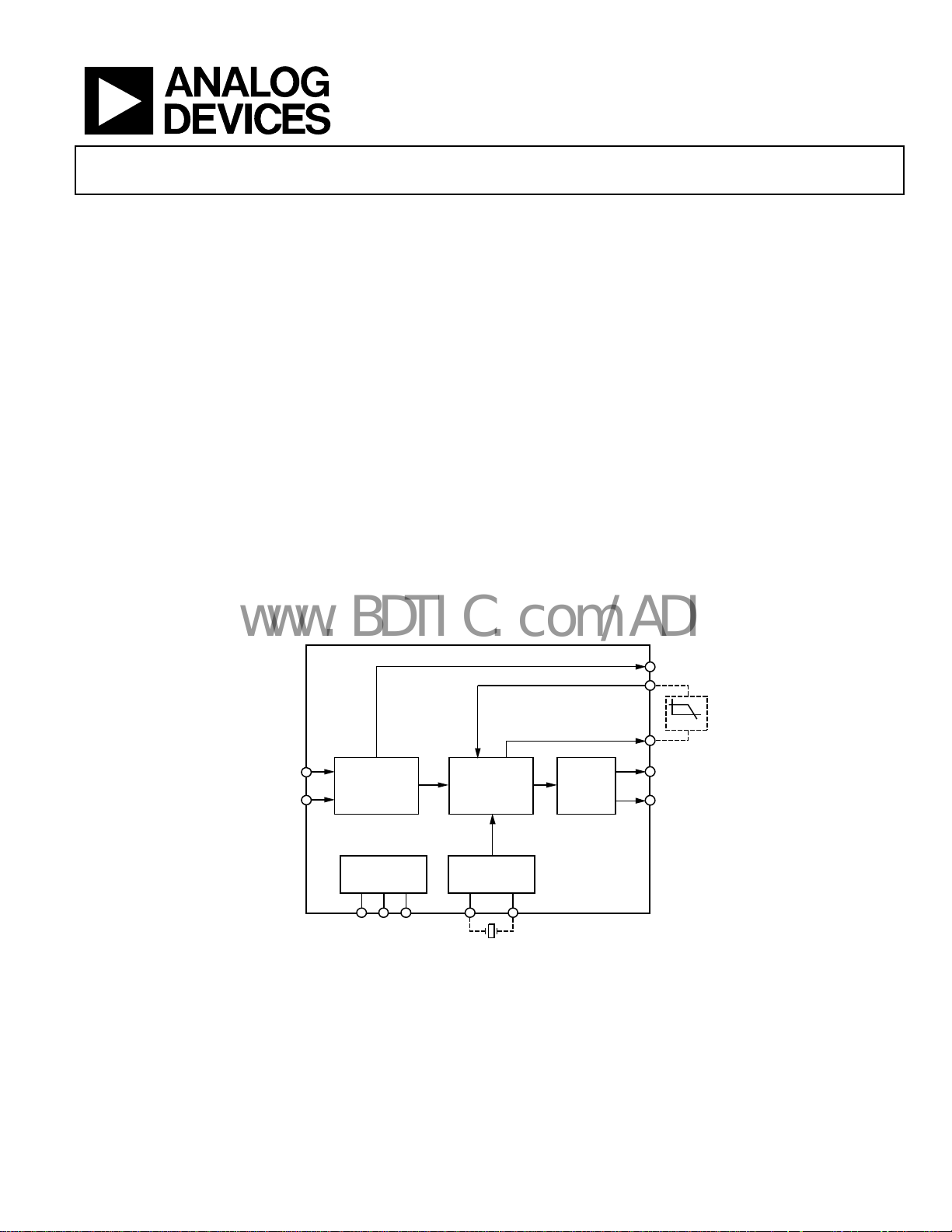
GENERAL DESCRIPTION
The AD9549 provides synchronization for many systems,
including synchronous optical networks (SONET/SDH). The
AD9549 generates an output clock, synchronized to one of two
external input references. The external references may contain
significant time jitter, also specified as phase noise. Using a
digitally controlled loop and holdover circuitry, the AD9549
continues to generate a clean (low jitter), valid output clock
during a loss of reference condition, even when both references
have failed.
The AD9549 operates over an industrial temperature range of
−40°C t
o +85°C.
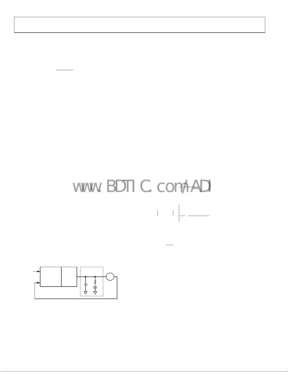
REFA_IN
REFB_IN
AD9549
REFERENCE
MONITORS
AND
SWITCHING
SERIAL PORT,
I/O LOGIC
DIGITAL INTERFACE
DIGITAL PLL
R
R, S DIVIDERS
HOLDOVER
SYSTEM CLOCK
MULTIPLIER
Figure 1. Basic Block Diagram
FDBK_IN
DAC_OUT
CLOCK
OUTPUT
DRIVERS
S1 TO S4
FILTER
OUT
OUT_CMOS
06744-001
Rev. 0
Information furnished by Analog Devices is believed to be accurate and reliable. However, no
responsibility is assumed by Anal og Devices for its use, nor for any infringements of patents or ot her
rights of third parties that may result from its use. Specifications subject to change without notice. No
license is granted by implication or otherwise under any patent or patent rights of Analog Devices.
Trademarks and registered trademarks are the property of their respective owners.
One Technology Way, P.O. Box 9106, Norwood, MA 02062-9106, U.S.A.
Tel: 781.329.4700 www.analog.com
Fax: 781.461.3113 ©2007 Analog Devices, Inc. All rights reserved.

AD9549
www.BDTIC.com/ADI
TABLE OF CONTENTS
Features .............................................................................................. 1
Applications....................................................................................... 1
General Description......................................................................... 1
Revision History ............................................................................... 2
Specifications..................................................................................... 3
DC Specifications ......................................................................... 3
AC Specifications.......................................................................... 5
Absolute Maximum Ratings............................................................ 8
ESD Caution.................................................................................. 8
Pin Configuration and Function Descriptions............................. 9
Typical Performance Characteristics ........................................... 12
Input/Output Termination Recommendations.......................... 15
Theory of Operation ...................................................................... 16
Overview...................................................................................... 16
PLL Core (DPLLC)..................................................................... 16
Phase Detector ............................................................................ 20
Digital Loop Filter Coefficients ................................................21
Closed-Loop Phase Offset......................................................... 22
Lock Detection............................................................................23
Reference Monitors.................................................................... 24
Reference Switchover................................................................. 25
Holdover ...................................................................................... 27
Output Frequency Range Control............................................ 30
Reconstruction Filter ................................................................. 30
FDBK Inputs ............................................................................... 30
Reference Inputs......................................................................... 31
SYSCLK Inputs ........................................................................... 31
Harmonic Spur Reduction........................................................ 33
Output Clock Drivers and 2× Frequency Multiplier............. 34
Frequency Slew Limiter............................................................. 35
Frequency Estimator.................................................................. 35
Status and Warnings .................................................................. 36
Thermal Performance.................................................................... 39
AD9549 Power-Up......................................................................... 40
Power-On Reset .......................................................................... 40
Programming Sequence ............................................................ 40
Power Supply Partitioning............................................................. 41
3.3 V Supplies.............................................................................. 41
1.8 V Supplies.............................................................................. 41
Serial Control Port ......................................................................... 42
Serial Control Port Pin Descriptions ....................................... 42
Operation of Serial Control Port.............................................. 42
The Instruction Word (16 Bits) ................................................ 43
MSB/LSB First Transfers ........................................................... 43
I/O Register Map............................................................................ 46
I/O Register Description ............................................................... 51
Serial Port Configuration (Reg 0000 to Reg 0005) ................ 51
Power-Down and Reset (Reg 0010 to Reg 0013) ................... 51
System Clock (Reg 0020 to Reg 0023)..................................... 52
Digital PLL Control and Dividers (Reg 0100 to Reg 0130).. 53
Free-Run (Single-Tone) Mode (Reg 01A0 to Reg 01AD)..... 55
Reference Selector/Holdover (Reg 01C0 to Reg 01C3)......... 56
Doubler and Output Drivers (Reg 0200 to Reg 0201)........... 57
Monitor (Reg 0300 to Reg 0335) .............................................. 57
Calibration (User-Accessible Trim) (Reg 0400 to Reg 0410) 61
Harmonic Spur Reduction (Reg 0500 to Reg 0509).............. 62
Sample Application Circuit........................................................... 64
Outline Dimensions ....................................................................... 65
Ordering Guide .......................................................................... 65
REVISION HISTORY
8/07—Revision 0: Initial Version
Rev. 0 | Page 2 of 68
AD9549
www.BDTIC.com/ADI
SPECIFICATIONS
DC SPECIFICATIONS
Unless otherwise noted, AVDD = 1.8 V ± 5%, AVDD3 = 3.3 V ± 5%, DVDD = 1.8 V ± 5%, DVDD_I/O = 3.3 V ± 5%. AVSS = 0 V,
DVSS = 0 V.
Table 1.
Parameter Min Typ Max Unit Test Conditions/Comments
SUPPLY VOLTAGE
DVDD_I/O (Pin 1) 3.135 3.30 3.465 V
DVDD (Pin 3, Pin 5, Pin 7) 1.71 1.80 1.89 V
AVDD3 (Pin 14, Pin 46, Pin 47, Pin 49) 3.135 3.30 3.465 V
AVDD3 (Pin 37) 1.71 3.30 3.465 V Pin 37 is typically 3.3 V, but can be set to 1.8 V
AVDD (Pin 11, Pin 19, Pin 23 to Pin 26, Pin 29,
Pin 30, Pin 36, Pin 42, Pin 44, Pin 45, Pin 53)
SUPPLY CURRENT
I
(Pin 14) 4.7 5.6 mA REFA, REFB buffers
AVDD3
I
(Pin 37) 3.8 4.5 mA CMOS output clock driver at 3.3 V
AVDD3
I
(Pin 46, Pin 47, Pin 49) 26 29 mA DAC output current source, fS = 1 GSPS
AVDD3
I
(Pin 36, Pin 42) 21 26 mA FDBK in, HSTL output clock driver (output
AVDD
I
(Pin 11) 12 15 mA REFA and REFB input buffer 1.8 V supply
AVDD
I
(Pin 19, Pin 23 to Pin 26, Pin 29,
AVDD
Pin 30, Pin 44, Pin 45)
I
(Pin 53) 41 49 mA DAC power supply
AVDD
I
(Pin 3, Pin 5, Pin 7) 254 265 mA Digital core
DVDD
I
(Pin 1) 4 6 mA Digital I/O (varies dynamically)
DVDD_I/O
LOGIC INPUTS (Except Pin 32) Pin 56 to Pin 61, Pin 64, Pin 9, Pin 10,
Input High Voltage (VIH) 2.0 DVDD_I/O V
Input Low Voltage (VIL) DVSS 0.8 V
Input Current (I
, I
) ±60 ±200 µA At VIN = 0 V and VIN = DVDD_I/O
INH
INL
Maximum Input Capacitance (CIN) 3 pF
CLKMODESEL (Pin 32) LOGIC INPUT Pin 32 only
Input High Voltage (VIH) 1.4 AVDD V
Input Low Voltage (VIL) AVSS 0.4 V
Input Current (I
, I
) −18 −50 µA At VIN = 0 V and VIN = AVDD
INH
INL
Maximum Input Capacitance (CIN) 3 pF
LOGIC OUTPUTS Pin 62 and bidirectional Pin 9, Pin 10,
Output High Voltage (VOH) 2.7 DVDD V IOH = 1 mA
Output Low Voltage (VOL) DVSS 0.4 V IOL = 1 mA
REFERENCE INPUTS Pin 12, Pin 13, Pin 15, Pin 16
Input Capacitance 3 pF
Input Resistance 8.5 11.5 14.5 kΩ Differential at Register 40F[1:0] = 00
Differential Operation
Common Mode Input Voltage1
(Applicable When DC-Coupled)
Differential Input Voltage Swing
1
Single-Ended Operation Register 040F[1:0] = 10
Input Voltage High (VIH) 2.0 AVDD3 V
Input Voltage Low (VIL) AVSS 0.8 V
Threshold Voltage AVDD3 −
Input Current 1 mA Single-ended operation
1.71 1.80 1.89 V
doubler turned on.)
194 255 mA Aggregate analog supply, including
system clock PLL
Pin 54, Pin 55, Pin 63
Pin 54, Pin 55, and Pin 63
1.5 AVDD3 −
0.2
V Differential operation; note that LVDS
signals must be ac-coupled
500 mV p-p Differential operation
0.66
AVDD3 −
0.82
AVDD3 −
0.98
V Register 040F[1:0] = 10 (other settings
possible)
Rev. 0 | Page 3 of 68
AD9549
www.BDTIC.com/ADI
Parameter Min Typ Max Unit Test Conditions/Comments
FDBK INPUT Pin 40, Pin 41
Input Capacitance 3 pF
Input Resistance 18 22 26 kΩ Differential
Differential Input Voltage Swing
SYSTEM CLOCK INPUT System clock inputs should always be ac-
SYSCLK PLL Bypassed
Input Capacitance 1.5 pF Single-ended, each pin
Input Resistance 2.4 2.6 2.8 kΩ Differential
Internally Generated DC Bias Voltage
Differential Input Voltage Swing
SYSCLK PLL Enabled
Input Capacitance 3 pF Single-ended, each pin
Input Resistance 2.4 2.6 2.8 kΩ Differential
Internally Generated DC Bias Voltage
Differential Input Voltage Swing
Crystal Resonator with SYSCLK PLL Enabled
Motional Resistance 9 100 Ω 25 MHz, 3.2 mm × 2.5 mm AT cut
CLOCK OUTPUT DRIVERS
HSTL Output Driver
Differential Output Voltage Swing
Common-Mode Output Voltage
CMOS Output Driver
Output Voltage High (VOH) AVDDX = 3.3 V 2.7 V IOH = 1 mA.
Output Voltage Low (VOL) AVDDX = 3.3 V 0.4 V IOL = 1 mA.
Output Voltage High (VOH) AVDDX = 1.8 V 1.4 V IOH = 1 mA.
Output Voltage Low (VOL) AVDDX = 1.8 V 0.4 V IOL = 1 mA.
TOTAL POWER DISSIPATION
All Blocks Running 1010 1250 mW Worst case over supply, temperature,
Power-Down Mode 24 mW Using either the Power-Down and Enable
Digital Power-Down Mode 515 650 mW
Default with SYSCLK PLL Enabled 905 1100 mW After reset or power up with fS = 1 GHz,
Default with SYSCLK PLL Disabled 895 1056 mW After reset or power up with fS = 1 GHz,
With REFA or REFB Power-Down 1046 mW One reference still powered up
With HSTL Clock Driver Power-Down 1036 mW
With CMOS Clock Driver Power-Down 1048 mW
1
Must be ≤ 0 V relative to AVDD3 (Pin 14) and ≥ 0 V relative to AVSS (Pin 33, Pin 43).
2
Relative to AVSS (Pin 33, Pin 43).
3
Must be ≤ 0 V relative to AVDD (Pin 36) and ≥ 0 V relative to AVSS (Pin 33, Pin 43).
2
225 mV p-p −12 dBm into 50 Ω; must be ac-coupled
coupled (both single-ended and differential)
2
3
2
3
0.93 1.17 1.38 V
632 mV p-p 0 dBm into 50 Ω
0.93 1.17 1.38 V
632 mV p-p 0 dBm into 50 Ω
1080 1280 1480 mV
Output driver static, see
Figure 12 for
output swing vs. frequency
2
0.7 0.88 1.06 V
Output driver static, see
Figure 14 for
output swing vs. frequency
process
register or PWRDOWN pin
S4 = 0, S1 to S3 = 1, f
SYSCLK
= 25MHz
S1 to S4 = 1
Rev. 0 | Page 4 of 68
AD9549
www.BDTIC.com/ADI
AC SPECIFICATIONS
Unless otherwise noted, fS = 1 GHz. DAC R
Table 2.
Parameter Min Typ Max Unit Test Conditions/Comments
REFERENCE INPUTS Pin 12, Pin 13, Pin 15, Pin 16
Frequency Range (Sine Wave) 10 750 MHz Minimum recommended slew rate: 40 V/s
Frequency Range (CMOS) 0.008 50 MHz
Frequency Range (LVPECL) 0.008 725 MHz
Frequency Range (LVDS) 0.008 725 MHz LVDS must be ac-coupled; lower frequency bound may
Minimum Slew Rate 0.04 V/ns
Minimum Pulse Width High 620 ps
Minimum Pulse Width Low 620 ps
FDBK INPUT Pin 40, Pin 41
Input Frequency Range 10 400 MHz
Minimum Differential Input Level 225 mV p-p −12 dBm into 50 Ω; must be ac-coupled
Minimum Slew Rate 40 V/s
SYSTEM CLOCK INPUT Pin 27, Pin 28
SYSCLK PLL Bypassed
Input Frequency Range 250 1000 MHz Maximum f
Duty Cycle 45 55 %
Minimum Differential Input Level 632 mV p-p 0 dBm into 50 Ω
SYSCLK PLL Enabled
VCO Frequency Range, Low Band 700 810 MHz When in the range, use the low VCO band exclusively
VCO Frequency Range, Auto Band 810 900 MHz When in the range, use the VCO Auto band select
VCO Frequency Range, High Band 900 1000 MHz When in the range, use the high VCO band exclusively
Maximum Input Rate of System Clock
PFD
Without SYSCLK PLL Doubler
Input Frequency Range 11 200 MHz
Multiplication Range 4 66 Integer multiples of 2, maximum PFD rate and system
Minimum Differential Input Level 632 mV p-p 0 dBm into 50 Ω
With SYSCLK PLL Doubler
Input Frequency Range 6 100 MHz
Multiplication Range 8 132 Integer multiples of 8
Input Duty Cycle 50 % Deviating from 50% duty cycle may adversely affect
Minimum Differential Input Level 632 mV p-p 0 dBm into 50 Ω
Crystal Resonator with SYSCLK PLL
Enabled
Crystal Resonator Frequency Range 10 50 MHz AT cut, fundamental mode resonator
Maximum Crystal Motional Resistance 100 Ω
CLOCK DRIVERS
HSTL Output Driver
Frequency Range 20 725 MHz
Duty Cycle 48 52 %
Rise/Fall Time (20-80%) 115 165 ps 100 Ω termination across OUT/OUTB, 2 pF load
Jitter (12 kHz to 20 MHz) 1.0 ps fIN = 19.44 MHz, f
HSTL Output Driver with 2× Multiplier
Frequency Range 400 725 MHz
Duty Cycle 45 55 %
Rise/Fall Time (20% to 80%) 115 165 ps 100 Ω termination across OUT/OUTB, 2 pF load
Sub-harmonic Spur Level −35 dBc Without correction
Jitter (12 kHz to 20 MHz) 1.1 ps fIN = 19.44 MHz, f
= 10 k. Power supply pins within the range specified in the DC Specifications section.
SET
be higher depending on size of decoupling capacitor
is 0.4 × f
100 MHz
clock frequency must be met
spurious performance.
See the
SYSCLK Inputs section for recommendations
See
Figure 12 for maximum toggle rate
input (see
input (see
Rev. 0 | Page 5 of 68
Figure 3 to Figure 11 for test conditions)
Figure 3 to Figure 11 for test conditions)
OUT
SYSCLK
= 155.52 MHz. 50 MHz system clock
OUT
= 622.08 MHz, 50 MHz system clock
OUT
AD9549
www.BDTIC.com/ADI
Parameter Min Typ Max Unit Test Conditions/Comments
CMOS Output Driver
(AVDD3/Pin 37) @ 3.3 V
Frequency Range 0.008 150 MHz
Duty Cycle 45 55 65 % With 20 pF load and up to 150 MHz
Rise/Fall Time (20-80%) 3 4.6 ns With 20 pF load
CMOS Output Driver
(AVDD3/Pin 37) @ 1.8 V
Frequency Range 0.008 40 MHz
Duty Cycle 45 55 65 % With 20 pF load and up to 40 MHz
Rise/Fall Time (20% to 80%) 5 6.8 ns With 20 pF load
HOLDOVER
Frequency Accuracy
OUTPUT FREQUENCY SLEW LIMITER
Slew Rate Resolution 0.54 111 Hz/sec P = 216 for minimum; P = 25 for maximum
Slew Rate Range 0 3 × 10
REFERENCE MONITORS
Loss of Reference Monitor
Operating Frequency Range 7.63 × 10³ 167 × 106Hz
Minimum Frequency Error for
Continuous REF Present Indication
Minimum Frequency Error for
Continuous REF Present Indication
Maximum Frequency Error for
Continuous REF Lost Indication
Maximum Frequency Error for
Continuous REF Lost Indication
Reference Quality Monitor
Operating Frequency Range 0.008 150 MHz
Frequency Resolution (Normalized) 0.2 ppm f
Frequency Resolution (Normalized) 408 ppm f
Validation Timer
Timing Range 32 × 10
Timing Range 65 × 10
DAC OUTPUT CHARACTERISTICS
DCO Frequency Range (1st Nyquist Zone) 10 450 MHz DPLL loop bandwidth sets lower limit
Output Resistance 50 Ω Single-ended (each pin internally terminated to AVSS)
Output Capacitance 5 pF
Full-Scale Output Current 20 31.7 mA Range depends on DAC R
Gain Error −10 +10 %FS
Output Offset 0.6 A
Voltage Compliance Range AVSS −
DIGITAL PLL
Minimum Open-Loop Bandwidth 0.1 Hz Dependent on the frequency of REFA/REFB, the DAC
Maximum Open-Loop Bandwidth 100 kHz Dependent on the frequency of REFA/REFB, the DAC
Minimum Phase Margin 0 10 Degrees Dependent on the frequency of REFA/REFB, the DAC
Maximum Phase Margin 85 90 Degrees Dependent on the frequency of REFA/REFB, the DAC
PFD Input Frequency Range ~0.008 ~24.5 MHz
Feedforward Divider Ratio 1 131,070 1, 2, …,65,535 or 2, 4, …, 131,070
Feedback Divider Ratio 1 131,070 1, 2, …, 65,535 or 2, 4, …, 131,070
See
Figure 14 for maximum toggle rate
See
Figure 13 for maximum toggle rate
See the
Holdover section
16
Hz/sec P = 216 for minimum; P = 25 for maximum
−16 ppm f
−19 % f
−32 ppm f
−35 % f
= 8 kHz
REF
= 155 MHz
REF
= 8 kHz
REF
= 155 MHz
REF
= 8 kHz; OOL divider = 65,535 for minimum; OOL
REF
divider = 1 for max (see the
Monitor
section)
= 155 MHz; OOL divider = 65,535 for minimum; OOL
REF
divider = 1 for maximum
See the
Reference Validation Timers section
0.50
−9
137 s PIO = 5
−6
2.8 × 10⁵s PIO = 16
+0.5 AVSS +
Outputs not dc-shorted to V
0.50
sample rate, and the P-, R-, and S-divider values
sample rate, and the P-, R-, and S-divider values
sample rate, and the P-, R-, and S-divider values
sample rate, and the P-, R-, and S-divider values
Reference Frequency
resistor
SET
SS
Rev. 0 | Page 6 of 68
AD9549
www.BDTIC.com/ADI
Parameter Min Typ Max Unit Test Conditions/Comments
LOCK DETECTION
Phase Lock Detector
Time Threshold Programming Range 0 2097 s FPFD_Gain = 200
Time Threshold Resolution 0.488 ps FPFD_Gain = 200
Lock Time Programming Range 32 × 10−9 275 s In power-of-2 steps
Unlock Time Programming Range 192 × 10−9 67 × 10−3s In power-of-2 steps
Frequency Lock Detector
Normalized Frequency Threshold
Programming Range
Normalized Frequency Threshold
Programming Resolution
Lock Time Programming Range 32 × 10−9 275 s In power-of-2 steps
Unlock Time Programming Range 192 × 10−9 67 × 10−3s In power-of-2 steps
DIGITAL TIMING SPECIFICATIONS
Time Required to Enter Power-Down 15 µs
Time Required to Leave Power-Down 18 µs
Reset Assert to High-Z Time
for S1 to S4 Configuration Pins
Reset Deassert to Low-Z Time
for S1 to S4 Configuration Pins
SERIAL PORT TIMING SPECIFICATIONS
SCLK Clock Rate (1/t
SCLK Pulse Width High, t
SCLK Pulse Width Low, t
SDO/SDIO to SCLK Setup Time, t
SDO/SDIO to SCLK Hold Time, t
) 25 50 MHz
CLK
HI
LO
DS
DH
SCLK Falling Edge to Valid Data on
SDIO/SDO, t
CSB to SCLK Setup Time, t
CSB to SCLK Hold Time, t
CSB Minimum Pulse Width High, t
DV
S
H
PWH
PROPAGATION DELAY
FDBK to HSTL Output Driver 2.8 ns
FDBK to HSTL Output Driver with 2×
Frequency Multiplier Enabled
FDBK to CMOS Output Driver 8.0 ns
FDBK Through S-Divider to CMOS
Output Driver
0 0.0021 FPFD_Gain = 200; normalized to (f
/R)2; see the
REF
Frequency Lock Detection section for details
5 ×
10
FPFD_Gain = 200; normalized to (f
−13
Frequency Lock Detection section for details
/R)2; see the
REF
60 ns Time from rising edge of RESET to high-Z on the S1, S2,
S3, S4 configuration pins
30 ns Time from falling edge of RESET to low-Z on the S1, S2,
S3, S4 configuration pins
Refer to
Figure 58 for all write-related serial port
parameters, maximum SCLK rate for readback is
governed by t
DV
8 ns
8 ns
1.93 ns
1.9 ns
11 ns
Refer to
Figure 56
1.34 ns
−0.4 ns
3 ns
7.3 ns
8.6 ns
Rev. 0 | Page 7 of 68
AD9549
www.BDTIC.com/ADI
ABSOLUTE MAXIMUM RATINGS
Table 3.
Parameter Rating
Analog Supply Voltage (AVDD) 2 V
Digital Supply Voltage (DVDD) 2 V
Digital I/O Supply Voltage
(DVDD_I/O)
DAC Supply Voltage (DAC_VDD) 3.6 V
Maximum Digital Input Voltage −0.5 V to DVDD_I/O + 0.5 V
Storage Temperature −65°C to +150°C
Operating Temperature Range −40°C to +85°C
Lead Temperature
(Soldering 10 sec)
Junction Temperature 150°C
Thermal Resistance1
θ
JA
θ
JB
θ
JC
1
The exposed pad on bottom of package must be soldered to ground in
order to achieve the specified thermal performance. See the Thermal
Performance section for more information.
3.6 V
300°C
25.2°C/W typical
13.9°C/W typical
1.7°C/W typical
Stresses above those listed under Absolute Maximum Ratings
may cause permanent damage to the device. This is a stress
rating only; functional operation of the device at these or any
other conditions above those indicated in the operational
section of this specification is not implied. Exposure to absolute
maximum rating conditions for extended periods may affect
device reliability.
ESD CAUTION
Rev. 0 | Page 8 of 68
AD9549
T
www.BDTIC.com/ADI
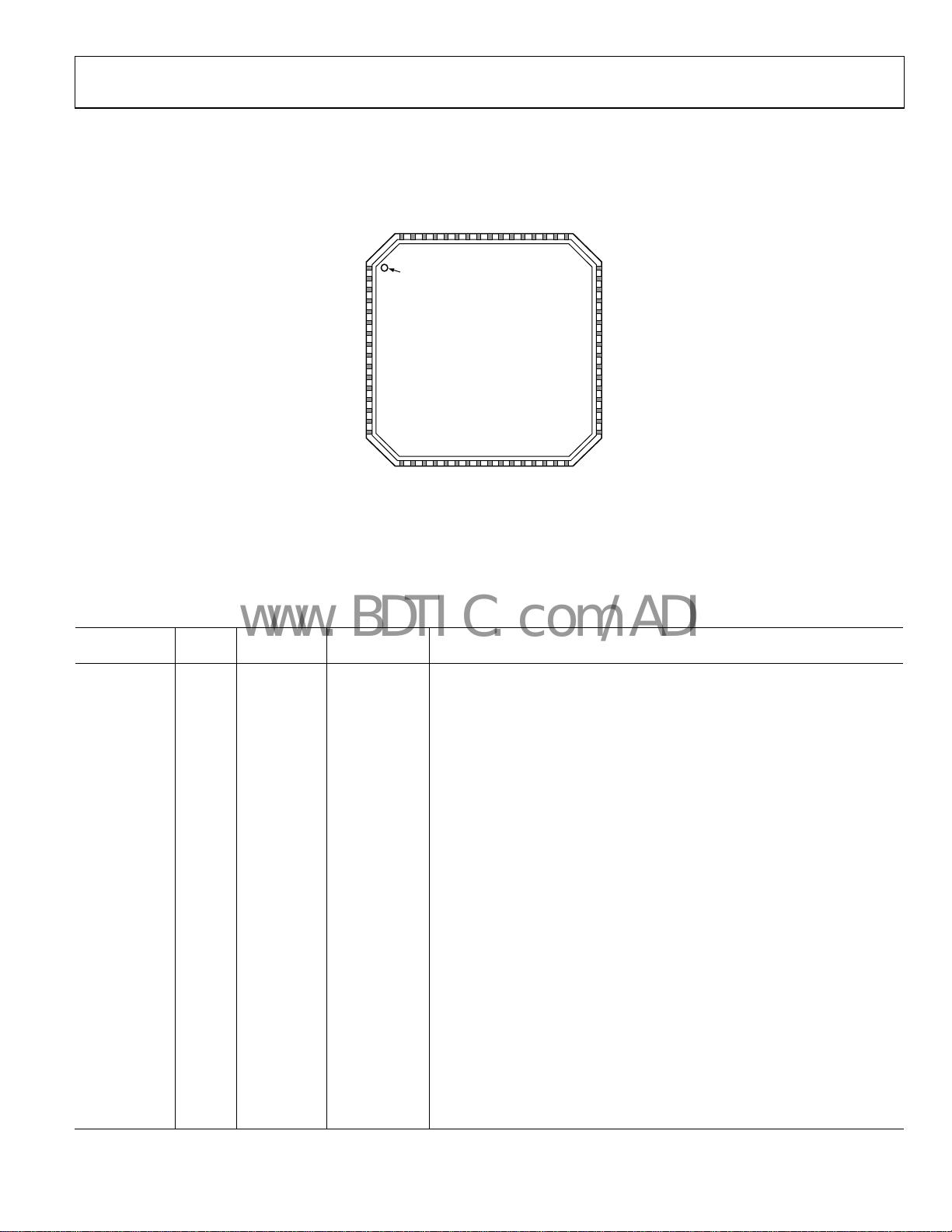
PIN CONFIGURATION AND FUNCTION DESCRIPTIONS
S4S3AVD D
AVSS
DAC_OUTB
DAC_OUT
AVDD3
49
DAC_RSET
48
AVDD3
47
AVDD3
46
AVD D
45
AVD D
44
AVSS
43
AVD D
42
FDBK_IN
41
FDBK_INB
40
AVSS
39
OUT_CMOS
38
AVDD3
37
AVD D
36
OUT
35
OUTB
34
AVSS
33
DVDD_I/O
DVSS
DVDD
DVSS
DVDD
DVSS
DVDD
DVSS
AVD D
REFA_IN
REFA_INB
AVD D3
REFB_IN
REFB_INB
SCLK
SDIO
SDO
CSB
IO_UPDATE
RESET
PWRDOWN
HOLDO VER
646362616059585756555453525150
PIN 1
1
INDICATOR
2
3
4
5
6
7
8
9
S1
10
S2
11
12
13
14
15
16
REFSELEC
AD9549
TOP VIEW
(Not to Scale)
NC = NO CONNECT
171819202122232425262728293031
NC
NC
AVD D
AVD D
AVD D
AVD D
AVD D
AVD D
AVD D
PFD_VRT
PFD_VRB
PFD_RSET
SYSCLK
SYSCLKB
32
LOOP_FILTER
CLKMODESEL
06744-002
Figure 2. 64-Lead LFCSP Pin Configuration
Table 4. Pin Function Descriptions
Input/
Ou
Pin No.
tput
Pin Type Mnemonic Description
1 I Power DVDD_I/O I/O Digital Supply.
2, 4, 6, 8 I Power DVSS Digital Ground. Connect to ground.
3, 5, 7 I Power DVDD Digital Supply.
9, 10, 54, 55 I/O 3.3 V CMOS S1, S2, S3, S4
Configurable I/O Pins. These pins are configured under program control (see
the Status and Warnings section) and do not have internal pull-up/pull-down
esistors.
r
11, 19, 23 to
I Power AVDD Analog Supply. Connect to a nominal 1.8 V supply.
26, 29, 30, 36,
42, 44, 45, 53
12 I
Differential
nput
I
REFA_IN
Frequency/Phase Reference A Input. This inter
nally biased input is typically accoupled and, when configured as such, can accept any differential signal with
single-ended swing between 0.4 V and 3.3 V. If dc-coupled, LVPECL or CMOS
input is preferred.
13 I
Differential
nput
I
REFA_INB
Complementary Frequency/Phase Reference A Input. Complementary signal
to the input pr
ovided on Pin 12. If using a single-ended, dc-coupled CMOS
signal into REFA_IN, bypass this pin to ground with a 0.01 F capacitor.
14, 46, 47, 49 I Power AVDD3 Analog Supply. Connect to a nominal 3.3 V supply.
15 I
Differential
nput
I
REFB_IN
Frequency/Phase Reference B Input. This internally biased input is typically accoupled and, when configured as such, can accept any differential signal with
single-ended swing between 0.4 V and 3.3 V. If dc-coupled, LVPECL or CMOS
input is preferred.
16 I
Differential
nput
I
REFB_INB
Complementary Frequency/Phase Reference B Input. Complementary signal to
the input provided on Pin 15. If using a single-ended, dc-coupled CMOS signal
into REFB_IN, bypass this pin to ground with a 0.01 F capacitor.
17, 18 NC No Connect. These are excess, unused pins that can be left floating.
20, 21 O
PFD_VRB,
T
PFD_VR
These pins must be capacitively decoupled. See the Phase Detector Pin
onnections section for details.
C
Rev. 0 | Page 9 of 68
AD9549
www.BDTIC.com/ADI
Input/
Pin No.
22 O
27 I
28 I
31 O LOOP_FILTER
32 I 1.8 V CMOS CLKMODESEL
33, 39, 43, 52 O GND AVSS Analog Ground. Connect to ground.
34 O 1.8 V HSTL OUTB
35 O 1.8 V HSTL OUT
37 I Power AVDD3
38 O 3.3 V CMOS OUT_CMOS
40 I
41 I
48 O
50 O
51 O
56 I/O 3.3 V CMOS REFSELECT
57 I/O 3.3 V CMOS HOLDOVER
58 I 3.3 V CMOS PWRDOWN
59 I 3.3 V CMOS RESET
60 I 3.3 V CMOS IO_UPDATE
Output Pin Type Mnemonic Description
Current Set
esistor
R
Differential
nput
I
Differential
nput
I
Differential
nput
I
Differential
nput
I
Current Set
esistor
R
Differential
utput
O
Differential
utput
O
PFD_RSET
SYSCLK
SYSCLKB
FDBK_INB
FDBK_IN
DAC_RSET
DAC_OUT
DAC_OUTB
Connect a 5 kΩ resistor from this pin to ground (see the Phase Detector Pin
onnections section).
C
System Clock Input. The system clock input has internal dc biasing and should
alwa
ys be ac-coupled, except when using a crystal. Single-ended 1.8 V CMOS
can also be used but can introduce a spur caused by an input duty cycle that is
not 50%. When using a crystal, tie the CLKMODESEL pin to AVSS, and connect
crystal directly to this pin and Pin 28.
Complementary System Clock. Complementary signal to the input provided
on P
in 27. Use a 0.01 F capacitor to ground on this pin if the signal provided
on Pin 27 is single-ended.
System Clock Multiplier Loop Filter. When using the fr
drive the system clock, an external loop filter must be constructed and
attached to this pin. This pin is pulled high when the system clock PLL is
bypassed and can be left floating in this mode. See Figure 44 for a diagram of
the system cloc
Clock Mode Select. Set to GND when connecting a crystal to the system clock
in 27 and Pin 28). Pull up to 1.8 V when using either an oscillator or an
input (P
external clock source. This pin can be left floating when the system clock PLL is
bypassed. (See the SYSCLK Inputs section for details on the use of this pin.)
Complementary HSTL Output. See the Specifications and Primary 1.8 V
erential HSTL Driver sections for details.
Diff
HSTL Output. See the Specifications and Primary 1.8 V Differential HSTL Driver
tions for details.
sec
Analog Supply for CMOS Output Driver: This pin
1.8 V. This pin should be powered even if the CMOS driver is not used. See the
Power Supply Partitioning section for power supply partitioning.
CMOS Output. See the Specifications section and the Output Clock Drivers and
requency Multiplier section. This pin is 1.8 V CMOS if Pin 37 is set to 1.8 V.
2× F
Complementary Feedback Input. In standard operating mode, this pin is
c
onnected to the filtered DAC_OUTB output. This internally biased input is
typically ac-coupled, and when configured as such, can accept any differential
signal whose single-ended swing is at least 400 mV.
Feedback Input. In standard operating mode
filtered DAC_OUT output
DAC Output Current Setting Resistor. Connect a resistor (usually 10 kΩ) from
this pin to GND
DAC Output. This signal should be filtered and sent back on chip through
FDBK_IN input. This pin has an internal 50 Ω pull-down resistor.
Complimentary DAC Output. This signal should be filtered and sent back on
chip thr
ough FDBK_INB input. This pin has an internal 50 Ω pull-down resistor.
Reference Select Input. In manual mode, the REFSELECT pin operates as a high
impedanc
output pin. Logic 0 (low) indicates/selects REFA. Logic 1 (high) indicates/selects
REFB. There is no internal pull-up/pull-down resistor on this pin.
Holdover (Active High). In manual holdover mode, this pin is used to force the
AD9549 in
holdover status. There is no internal pull-up/pull-down resistor on this pin.
Power-Down. When this active high pin is asserted, the device becomes
inac
pull-down resistor.
Chip Reset. When this active high pin is a
that on power-up, a 10 s reset pulse is internally generated when the power
supplies reach a threshold and stabilize. This pin has an internal 50 kΩ pulldown resistor.
I/O Update. A logic transition from 0 to 1 on this pin transf
port registers to the control registers (see the Write section). This pin has an
ternal 50 kΩ pull-down resistor.
in
e input pin, while in automatic mode, it operates as a low impedance
to holdover mode. In automatic holdover mode, it indicates
tive and enters the full power-down state. This pin has an internal 50 kΩ
equency multiplier to
k PLL loop filter.
is normally 3.3 V but can be
, this pin is connected to the
. See the DAC Output section.
sserted, the chip goes into reset. Note
ers data from the I/O
Rev. 0 | Page 10 of 68
AD9549
www.BDTIC.com/ADI
Input/
Pin No.
61 I 3.3 V CMOS CSB
62 O 3.3 V CMOS SDO
63 I/O 3.3 V CMOS SDIO
64 I 3.3 V CMOS SCLK
Exposed Die
Pad
Output Pin Type Mnemonic Description
Chip Select. Active low. When programming a device, this pin must be held
w. In systems where more than one AD9549 is present, this pin enables
lo
individual programming of each AD9549. This pin has an internal 100 kΩ pullup resistor.
Serial Data Output. When the device is in 3-wire mode, data is r
There is no internal pull-up/pull-down resistor on this pin.
Serial Data Input/Output. When
this pin. In 2-wire mode, data reads and writes both occur on this pin. There is
no internal pull-up/pull-down resistor on this pin.
Serial Programming Clock. Data clock for serial programming. This pin has an
ternal 50 kΩ pull-down resistor.
in
O GND AVSS Analog Ground. Connect to ground.
the device is in 3-wire mode, data is written via
ead on this pin.
Rev. 0 | Page 11 of 68
AD9549
–
–
–
–
–
–
www.BDTIC.com/ADI
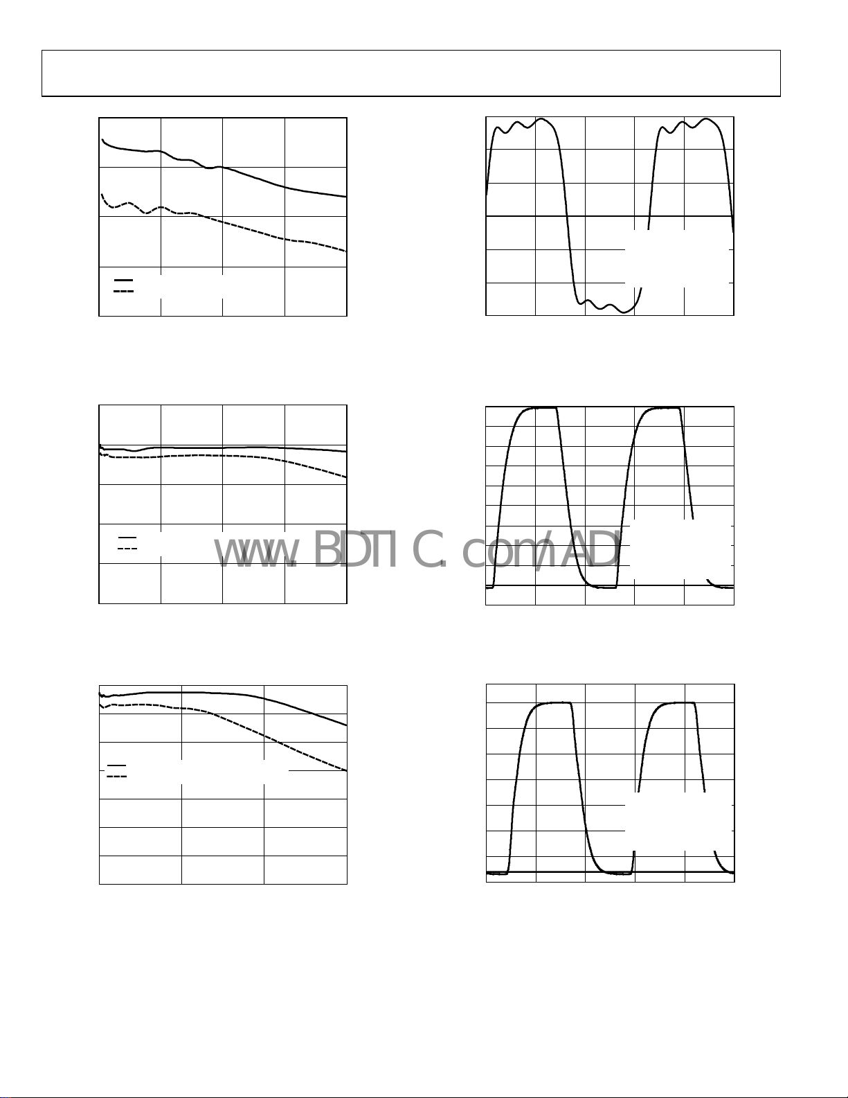
TYPICAL PERFORMANCE CHARACTERISTICS
Unless otherwise noted, AVDD, AVDD3, and DVDD at nominal supply voltage; fS = 1 GHz, DAC R
–80
70
RMS JITTER (12kHz TO 20MHz): 0.18p s
RMS JITTER (50kHz TO 80MHz): 0.24p s
70
–80
= 10 k.
SET
RMS JITTER (12kHz TO 20MHz): 1.09p s
RMS JITTER (50kHz TO 80MHz): 1.14p s
–90
–100
–110
–120
PHASE NOISE (dBc/Hz)
–130
–140
–150
10 100 1k 10k 100k 1M 10M 100M
FREQUENCY OF FSET (Hz)
Figure 3. Additive Phase Noise at HSTL Output Driver, SYSCLK = 1 GHz
PLL Bypassed), f
(SYSCLK
= 311.04 MHz, DPLL Loop BW = 1 kHz
f
OUT
70
–80
–90
–100
–110
–120
PHASE NOISE (dBc/Hz)
–130
RMS JITT ER (12kHz TO 20MHz): 0.36p s
RMS JITT ER (50kHz TO 80MHz): 0.42p s
= 19.44 MHz,
REF
–90
–100
–110
–120
PHASE NOISE (dBc/Hz)
–130
–140
–150
06744-003
10 100 1k 10k 100k 1M 10M 100M
FREQUENCY OF FSET (Hz)
06744-006
Figure 6. Additive Phase Noise at HSTL Output Driver, SYSCLK = 1 GHz
(SYSCLK PLL
50 MHz), f
Enabled and Driven by R&S SMA100 Signal Generator at
= 19.44 MHz, f
REF
= 622.08 MHz, DPLL Loop BW = 1 kHz,
OUT
System Clock Doubler Enabled, HSTL Doubler Enabled
PHASE NOISE (dBc/Hz)
70
–80
–90
–100
–110
–120
–130
RMS JITT ER (12kHz TO 20MHz): 1.0p s
RMS JITT ER (50kHz TO 80MHz): 1.2p s
–140
–150
10 100 1k 10k 100k 1M 10M 100M
FREQUENCY OF FSET (Hz)
Figure 4. Additive Phase Noise at HSTL Output Driver, SYSCLK = 1 GHz
(SYSCLK
PLL Bypassed), f
= 19.44 MHz, f
REF
= 622.08 MHz,
OUT
DPLL Loop BW = 1 kHz, HSTL Output Doubler Enabled
70
–80
–90
–100
–110
–120
PHASE NOISE (dBc/Hz)
–130
–140
–150
10 100 1k 10k 100k 1M 10M 100M
RMS JITTER (12kHz TO 20MHz): 1.01p s
RMS JITTER (50kHz TO 80MHz): 1.04p s
FREQUENCY OF FSET (Hz)
Figure 5. Additive Phase Noise at HSTL Output Driver, SYSCLK = 1 GHz
(SYSCLK PLL
Enabled Driven by R&S SMA100 Signal Generator at 50 MHz),
= 19.44 MHz, f
f
REF
= 311.04 MHz, DPLL Loop BW = 1 kHz
OUT
06744-004
(SYSCLK PLL
06744-005
Rev. 0 | Page 12 of 68
–140
–150
10 100 1k 10k 100k 1M 10M 100M
FREQUENCY OF FSET (Hz)
Figure 7. Additive Phase Noise at HSTL Output Driver, SYSCLK = 1 GHz
Enabled and Driven by R&S SMA100 at 50 MHz), f
= 155.52 MHz, SYSCLK Doubler Enabled, DPLL Loop BW =1 kHz
f
OUT
70
–80
–90
–100
–110
–120
PHASE NOISE (dBc/Hz)
–130
–140
–150
10 100 1k 10k 100k 1M 10M 100M
RMS JITT ER (12kHz TO 20MHz): 1.07p s
RMS JITT ER (50kHz TO 80MHz): 1.16p s
FREQUENCY OF FSET (Hz)
= 19.44 MHz,
REF
Figure 8. Additive Phase Noise at HSTL Output Driver, SYSCLK = 1 GHz
(SYSCLK PLL
Enabled and Driven by R&S SMA100 Signal Generator at
50 MHz), f
= 8 kHz, f
REF
= 155.52 MHz, DPLL Loop BW = 10 Hz
OUT
06744-007
06744-008
AD9549
–
–
www.BDTIC.com/ADI
2.0
1.5
1.0
0.5
12kHz TO 20MHz RMS JITTER (ps)
0
10 30 50 70 90
SYSTEM CLOCK PLL INPUT FREQUENCY (MHz)
Figure 9. 12 kHz to 20 MHz RMS Jitter v
SYSCLK = 1 GHz, f
70
–80
–90
–100
–110
= 19.44 MHz, f
REF
RMS JITT ER (12kHz TO 20MHz): 1.26p s
RMS JITT ER (50kHz TO 80MHz): 1.30p s
06744-009
s. System Clock PLL Input Frequency,
= 155.52 MHz
OUT
70
–80
–90
–100
–110
–120
PHASE NOISE (dBc/Hz)
–130
–140
–150
10 100 1k 10k 100k 1M 10M
RMS JITTER (12kHz TO 20M Hz): 4.2ps
FREQUENCY OFFSET (Hz)
06744-011
Figure 11. Additive Phase Noise at HSTL Output Driver, SYSCLK = 500 MHz
(SYSCLK
PLL Disabled), f
= 10.24 MHz, f
REF
= 20.48 MHz,
OUT
DPLL Loop BW = 1 kHz
–120
PHASE NOISE (dBc/Hz)
–130
–140
–150
10 100 1k 10k 100k 1M 10M 100M
FREQUENCY OF FSET (Hz)
Figure 10. Additive Phase Noise at HSTL Output Driver, SYSCLK = 1 GHz
(SYSCLK PLL
Enabled and Driven by a 25 MHz Fox Crystal Oscillator),
f
= 19.44 MHz, f
REF
= 155.52 MHz, DPLL Loop BW = 1 kHz
OUT
06744-010
Rev. 0 | Page 13 of 68
AD9549
www.BDTIC.com/ADI
650
600
0.6
0.4
0.2
550
(mV)
500
NOM SKEW 25°C, 1.8V SUPPLY
SLOW SKEW 90°C, 1. 7V SUPPLY
450
0 200 400 600 800
(MHz)
06744-012
Figure 12. HSTL Output Driver Single-Ended Peak-to-Peak Amplitude vs.
Toggle Rate (100 Ω Across Differential Pair)
2.5
2.0
1.5
(V)
1.0
NOM SKEW 25° C, 1.8V SUPPLY (20pF)
0.5
0
0 1020304
SLOW S KEW 90°C, 1.7V SUPPL Y (20pF )
(MHz)
0
06744-013
Figure 13. CMOS Output Driver Peak-to-Peak Amplitude vs. Toggle Rate
VDD3 = 1.8 V) with 20 pF Load
(A
0
(V)
FREQUENCY= 600MHz
(20→80%) = 104ps
T
–0.2
–0.4
–0.6
0 0.5 1.0 1.5 2.0 2.5
RISE
T
FALL
V p-p = 1. 17V DIFF.
DUTY CYCLE = 50%
(ns)
(80→20%) = 107ps
Figure 15. Typical HSTL Output Waveform, Nominal Conditions,
DC-Coupl
1.8
1.6
1.4
1.2
1.0
0.8
(V)
0.6
0.4
0.2
0
–0.2
0 20 40 60 80 100
Figure 16. Typical CMOS Output Dr
ed, Differential Probe Across 100 Ω load
FREQUENCY= 20MHz
T
(20→80%) = 5.5ns
RISE
T
(80→20%) = 5.9ns
FALL
V p-p = 1.8V
DUTY CYCLE = 53%
(ns)
iver Waveform (@ 1.8 V),
Nominal Conditions, Estimated Capacitance: 5 pF
06744-015
06744-016
3.5
3.0
2.5
2.0
(V)
1.5
1.0
0.5
NOM SKEW 25°C, 3.3V SUPPLY (20pF)
SLOW SKEW 90°C, 3.0V SUPPLY (20pF)
0
0 50 100 150
(MHz)
06744-014
Figure 14. CMOS Output Driver Peak-to-Peak Amplitude vs. Toggle Rate
VDD3 = 3.3 V) with 20 pF Load
(A
Rev. 0 | Page 14 of 68
3.3
2.8
2.3
1.8
(V)
1.3
0.8
0.3
–0.2
0 102030405
FREQUENCY= 40MHz
T
(20→80%) = 2.25ns
RISE
T
FALL
V p-p = 3.3V
DUTY CYCLE = 52%
(ns)
(80→20%) = 2.6ns
0
Figure 17. CMOS Output Driver Waveform (@ 3.3 V), Nominal Conditions,
Esti
mated Capacitance: 5 pF, f
= 20 MHz
OUT
06744-017
AD9549
www.BDTIC.com/ADI
INPUT/OUTPUT TERMINATION RECOMMENDATIONS
0.01µF
AD9549
1.8V
HSTL
OUTPUT
100Ω
0.01µF
DOWNSTREAM
DEVICE
(HIGH-Z)
Figure 18. AC-Coupled HSTL Output Driver
AD9549
1.8V
HSTL
OUTPUT
50Ω
AVDD/2
50Ω
DOWNSTREAM
DEVICE
(HIGH-Z)
Figure 19. DC-Coupled HSTL Output Driver
0.01µF
100Ω
(OPTIONAL)
0.01µF
06744-018
AD9549
SELF-BIASING
REF INPUT
06744-020
Figure 20. Reference Input
0.1µF
100Ω
(OPTIONAL)
0.1µF
06744-019
AD9549
SELF-BIASING
FDBK INPUT
06744-021
Figure 21. FDBK Input
Rev. 0 | Page 15 of 68
AD9549
www.BDTIC.com/ADI
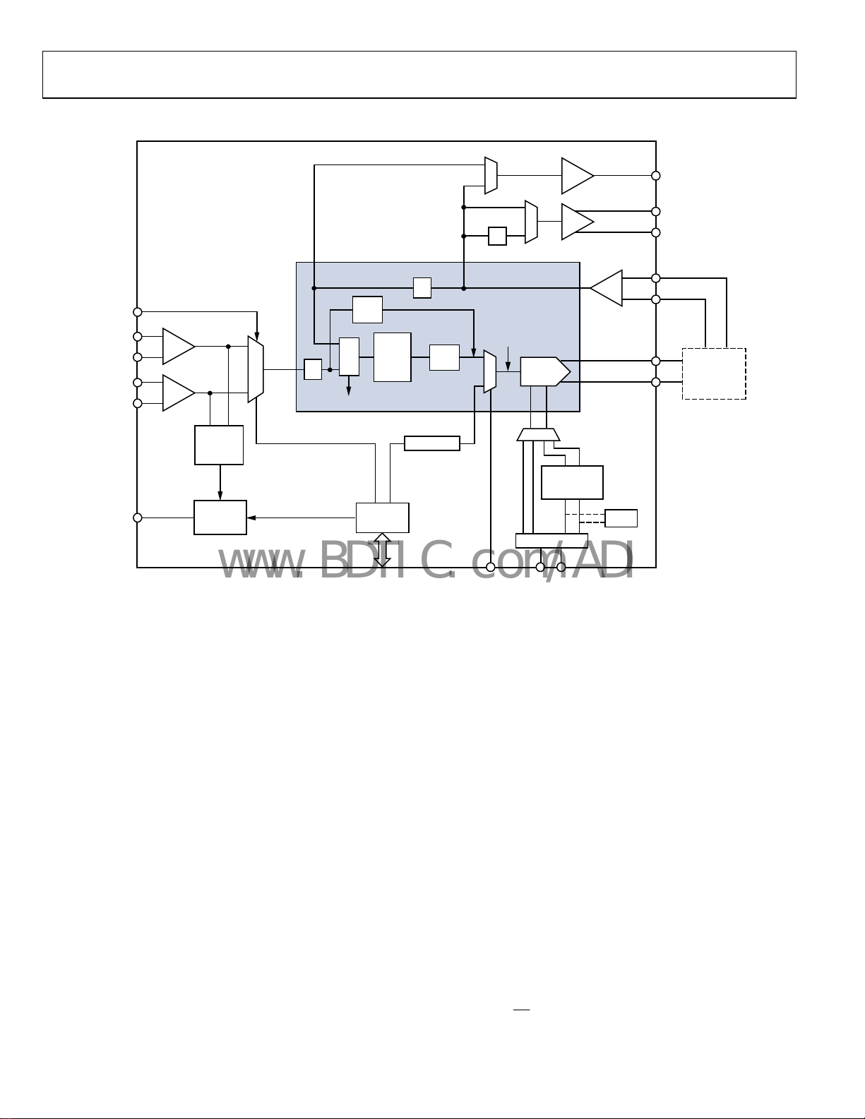
THEORY OF OPERATION
OUT_CMOS
REFSELECT
REFA_IN
REFB_IN
S1 TO S4
INPUT
MONITOR
OOL AND LO R
IRQ AND
STATUS
LOGIC
REF
÷R
REF_CNTRL
FREQ
EST.
PROG.
DIGITAL
PFD
LOOP
FILTER
LOCK DETECT
CONTROL
LOGIC
DIGITAL
INTERFACE
Figure 22. Detailed Block Diagram
OVERVIEW
The AD9549 provides a clocking output that is directly related
in phase and frequency to the selected (active) reference (REFA
or REFB) but has a phase noise spectrum primarily governed by
the system clock. A wide band of reference frequencies is supported. Jitter existing on the active reference is greatly reduced
by a programmable digital filter in the digital phase-locked loop
(PLL), which is the core of this product. The AD9549 supports
both manual and automatic holdover. While in holdover, the
AD9549 continues to provide an output as long as the system
clock is maintained. The frequency of the output during holdover is an average of the steady state output frequency prior to
holdover.
Also offered are manual and automatic switchover modes for
nging between the two references, should one become
cha
suspect or lost. A digitally controlled oscillator (DCO) is
implemented using a direct digital synthesizer (DDS) with an
integrated output DAC, clocked by the system clock. A bypassable PLL-based frequency multiplier is present enabling use of
an inexpensive, low frequency source for the system clock. For
best jitter performance, the system clock PLL should be bypassed,
and a low noise, high frequency system clock should be provided
directly. Sampling theory sets an upper bound for the DDS
output frequency at 50% of f
(where fS is the DAC sample rate),
S
2×
÷S
SLEW
HOLDOVER
DIGITAL PLL CORE
FREQUENCY
LIMIT
HOLDOVER SYSCLK
TUNING
WORD
DDS/DAC
LOW NOISE
MULTIPLIER
SYSCLK PORT
but a practical limitation of 40% of f
CLOCK
AMP
OUT
FDBK
EXTERNAL
ANALOG
LOW-PASS
FILTER
is generally recommended
S
to allow for the selectivity of the required off-chip
reconstruction filter. The output signal from the reconstruction
filter is fed back to the AD9549, both to complete the PLL and
to be processed through the output circuitry. The output
circuitry includes HSTL and CMOS output buffers, as well as a
frequency doubler for designs that need to provide frequencies
above the Nyquist level of the DDS.
The individual functional blocks are described in the following
secti
ons.
PLL CORE (DPLLC)
The digital phase-locked loop core (DPLLC) includes the
frequency estimation block and the digital phase lock control
block driving the DDS.
The start of the DPLLC signal chain is the reference signal, f
which appears on REFA or REFB inputs. The frequency of this
signal can be divided by an integer factor of R via the feedforward divider. The output of the feedforward divider is routed to
the phase/frequency detector (PFD). Therefore, the frequency
at the input to the PFD is given by
f
R
=
f
PFD
R
06744-022
,
R
Rev. 0 | Page 16 of 68
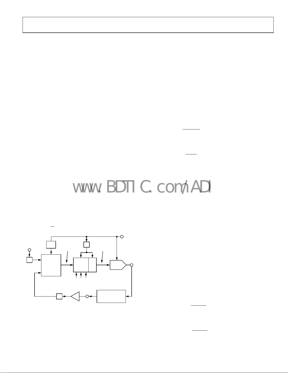
AD9549
www.BDTIC.com/ADI
The PFD outputs a time series of digital words that are routed
to the digital loop filter. The digital filter implementation offers
many advantages: The filter response is determined by numeric
coefficients rather than discrete component values. There is no
aging of components and therefore, no drift of component value
over time. There is no thermal noise in the loop filter, and there
is no control node leakage current (which causes reference feedthrough in a traditional analog PLL).
The output of the loop filter is a time series of digital words.
T
hese words are applied to the frequency tuning input of a DDS
to steer the DCO frequency. The DDS provides an analog
output signal via an integrated DAC, effectively mimicking the
operation of an analog VCO.
The DPLLC can be programmed to operate in conjunction
ith an internal frequency estimator to help decrease the time
w
required to achieve lock. When the frequency estimator is
employed, frequency acquisition is accomplished in a two-step
process:
1. An es
timate is made of the frequency of f
. The phase
PFD
lock control loop is essentially inoperative during the
frequency estimation process. Once a frequency estimate is
made, it is delivered to the DDS so that its output frequency
is approximately equal to f
multiplied by S (the modulus
PFD
of the feedback divider).
2. The phas
e lock control loop becomes active and acts as a
servo to acquire and hold phase lock with the reference
signal.
As mentioned in Step 1, the DPLLC includes a feedback divider
hat allows the DCO to operate at an integer multiple (S) of f
t
This establishes a nominal DCO frequency (f
S
⎞
⎛
f
=
⎟
⎜
R
R
⎠
⎝
÷PFD
PHASE
DETECTO R
(TIME-TO-
DIGIT AL
SAMPLES
DELIVERED AT
DIV
THE CLK RAT E
LOOP
FILTER
αβ
FDBK_IN
÷S
Figure 23. AD9549 Digital PLL Block Diagram
÷P
CCI
ץ
PINS
SAMPLES
DELIVERED AT
SYSCLK RATE
EXTERNAL DAC
RECONSTRUCTION
REF
INPUT
÷R
f
CLK
DDS
CONVERTER)
), given by
DDS
DDS
FILTER
SYSCLK
DAC_OUT
PINS
PFD
Feedforward Divider (Divide-by-R)
The feedforward divider is an integer divider that allows
frequency prescaling of the REF source input signal while
maintaining the desired low jitter performance of the AD9549.
The feedforward divider is a programmable modulus divider
th very low jitter injection. The divider is capable of handling
wi
input frequencies as high as 750 MHz. The divider depth is 16-
Rev. 0 | Page 17 of 68
.
06744-023
bits cascaded with an additional divide-by-2. The divider
therefore is capable of integer division from 1 to 65,535 (index
of 1) or 2 to 131,070 (index of 2). The divider is programmed
via the I/O Register Map to trigger on either the rising (default)
or falling edge of the REF source input signal. Note that the
value stored in the R-divider register is one less than the actual
R-divider, so setting the R-divider register to zero results in an R
divider equal to one.
There is a lower bound on the value of R imposed by the phase
f
requency detector within the DPLLC, which has a maximum
operating frequency of f
, as explained in the Fine Phase
PFD[MAX]
Detector section. The R-Divider/2 bit must be set when REFA
r REFB is greater than 400 MHz. The user must also ensure
o
that R is chosen so that it satisfies the inequality
⎛
R
⎜
≥
ceil
⎜
f
⎝
⎞
f
R
⎟
⎟
][
MAXPFD
⎠
The upper bound is
f
⎛
⎞
≤
floor
R
R
⎜
⎟
kHz8
⎝
⎠
where the ceil(x) function yields the nearest integer ≥ x.
For example, if f
=155 MHz and f
R
= 24.5 MHz, then
PFD[MAX]
ceil (155/24.5) = 7, so R must be ≥ 7.
Feedback Divider (Divide-by-S)
The feedback divider is an integer divider allowing frequency
multiplication of the REF signal that appears at the input of the
phase detector. It is capable of handling frequencies well above
the Nyquist limit of the DDS. The divider depth is 16-bits cascaded with an additional divide-by-2. The divider is therefore
capable of integer division from 1 to 65,535 (index of 1) or 2 to
131,070 (index of 2). The divider is programmed via the I/O
Register Map to trigger on either the rising (default) or falling
edge of the feedback signal. Note that the value stored in the SDivider register is one less than the actual R-divider, so setting
the S-Divider register to zero results in an S-divider equal to one.
The feedback divider must be programmed within certain
b
oundaries. The S-Divider/2 bit must be set when FDBK_IN is
greater than 400 MHz. The upper boundary on the feedback
divider is the lesser of the maximum programmable value of
S and the maximum practical output frequency of the DDS
(~ 40% f
divider index of 1 and S
). Two equations are given—S
S
for an index of 2.
max2
⎛
%40
Rf
S
⎜
= 535,65,
MAX1
min
⎜
f
R
⎝
S
for a feedback
max1
⎞
⎟
⎟
⎠
or
⎛
%40
Rf
S
⎜
= 070,131,
S
where
sample rate, and
min
2
MAX
⎜
f
R
⎝
R is the modulus of the feedforward divider, f
f
is the input reference frequency.
R
⎞
⎟
⎟
⎠
is the DAC
S
AD9549
C
www.BDTIC.com/ADI
The DCO has a minimum frequency, f
DCO[MIN]
(see the DAC
Output Characteristics section of the AC Specifications table).
This i
mposes a lower bound, S
, on the feedback divider
MIN
value as well.
⎞
⎞
][RMINDCO
⎟
⎟
⎟
⎟
⎠
⎠
MIN
= 1,max
⎛
⎛
f
⎜
⎜
RS
⎜
⎜
f
⎝
⎝
Note that reduced DCO frequencies result in worse jitter
erformance (a consequence of the reduced slew rate of the
p
sinusoid generated by the DDS).
Forward and Reverse FEC Clock Scaling
The feedforward divider (divide-by-R) and feedback divider
(divide-by-S) enable FEC clock scaling. For instance, to
multiply the incoming signal by 255/237, set the S-divider to
255 and the R-divider to 237. One should be careful to abide by
the limitations on the R- and S-dividers, and make sure the
phase detector input frequency is within specified limits.
Phase Detector
The phase detector is composed of two detectors: a coarse phase
detector and a fine phase detector. The two detectors operate in
parallel. Both detectors measure the duration (t) of the pulses
generated by a conventional three-state phase/frequency detector.
Together, the fine and coarse phase detectors produce a digital
ord that is a time-to-digital conversion of the separation
w
between the edge transitions of the prescaled reference signal
and the feedback signal.
If the fine phase detector is able to produce a valid result, this
r
esult alone serves as the phase error measurement. If the fine
phase detector is either in an overflow or underflow condition,
the phase error measurement uses the coarse phase detector
instead.
Digital Loop Filter
The digital loop filter integrates and low-pass filters the digital
phase error values delivered by the phase detector. The loop
filter response mimics that of a 2
nd
order RC network used to
filter the output of a typical phase detector and charge pump
combination as shown in
LK
PHASE/
FREQUENCY
DETECTOR
Figure 24. Typical Analog PLL Block Diagram
Figure 24.
CHANGE
PUMP
LOOP FILTER
R2
C1
C2
VCO
6744-024
The building blocks implemented on the AD9549, however, are
digital. A time-to-digital converter that produces digital values
proportional to the edge timing error between the CLK and
feedback signals replaces the phase-frequency detector and
charge pump. A digital filter that processes the edge timing
error samples from the time-to-digital converter replaces the
loop filter. A DDS replaces the VCO, which produces a frequency
Rev. 0 | Page 18 of 68
that is linearly related to the digital value provided by the loop
filter. This is shown in
Figure 25 with some additional detail.
The samples provided by the time-to-digital converter are
de
livered to the loop filter at a sample rate equal to the CLK
frequency (that is, f
/R). The loop filter is intended to oversam-
R
ple the time-to-digital converter output at a rate determined by
the P-divider. The value of P is programmable via the I/O
Register Map. It is stored as a 5-bit number, P
. The value of PIO
IO
is related to P by the equation
PIO
P = 2
where 5 ≤ P
≤ 16.
IO
Hence, the P-divider can provide divide ratios between 32 and
65,536 in p
ower-of-2 steps. With a DAC sample rate of 1 GHz,
the loop filter sample rate can range from as low as 15.26 kHz to
a maximum of 31.25 MHz. Coupled to the loop filter is a
cascaded comb integrator (CCI) filter that provides a sample
rate translation between the loop filter sample rate (f
the DDS sample rate, f
.
S
/P) and
S
The choice of P is important because it controls both the
r
esponse of the CCI filter and the sample rate of the loop filter.
In order to understand the method for determining a useful
value for P, it is first necessary to examine the transfer function
of the CCI filter.
2
jω
P
⎡
)(
ωH
CCI
1
=
⎢
1(
⎣
⎤
e
−
−
⎥
− jω
eP
⎦
or
0,1
=
ω
CCI
⎛
)(
=
ωH
−
⎜
⎜
−
p
⎝
2
ωP
ω
⎞
)cos(11
,
⎟
⎟
)cos(1
⎠
0
>
ω
To evaluate the response in terms of absolute frequency, make
e substitution
th
π
2
f
=
ω
f
S
where f
H
is the DAC sample rate and f is the frequency at which
S
is to be evaluated.
CCI
Analysis of this function reveals that the CCI magnitude
r
esponse follows a low-pass characteristic that consists of a
series of P lobes. The lobes are bounded by null points occurring at frequency multiples of f
/P. The peak of each successive
S
lobe is lower that its predecessor over the frequency range
between dc and ½f
response is a reflection about the vertical at ½f
the first lobe (which appears between dc and f
. For frequencies greater than ½fS, the
S
. Furthermore,
S
/P) exhibits a
S
monotonically decreasing response. That is, the magnitude is
unity at dc, and it steadily decreases with frequency until it
vanishes at the first null point (f
/P).
S
The null points imply the existence of transmission zeros placed
a
t finite frequencies. While transmission zeros placed at infinity
yield minimal phase delay, zeros placed closer to dc result in
AD9549
www.BDTIC.com/ADI
increased phase delay. Hence, the position of the first null point
has a significant impact on the phase delay introduced by the
CCI filter. This is an important consideration because excessive
phase delay negatively impacts the overall closed-loop response.
As a rule of thumb, choose a value for P so that the frequency of
the first null point (f
loop bandwidth or 1.5 times the frequency of CLK (f
The value of P thus calculated (P
in practice. Because P is programmed as P
define P
in terms of PIO so that P
MAX
The condition P
/P) is the greater of 80 times the desired
S
) is the largest usable value
MAX
, it is necessary to
IO
can be determined.
IOMAX
IO
≤ P
ensures that the impact of the phase
IOMAX
/R).
R
delay of the CCI filter on the phase margin of the loop does not
exceed 5°. P
=
P
IOMAX
can be expressed as
IOMAX
⎧
⎪
⎨
⎪
⎩
⎡
⎛
⎜
⎢
logfloor,16min,5max
⎜
80
⎢
⎝
⎣
f
f
S
LOOP
⎤
⎡
⎞
⎟
⎥
⎟
⎥
⎠
⎦
⎛
f
2
S
⎜
⎢
logfloor,
22
⎜
f
3
⎢
⎣
REF
⎝
With a properly chosen value for P, the closed-loop response of
the digital PLL is primarily determined by the response of the
digital loop filter. Flexibility in controlling the loop filter
response translates directly into flexibility in the range of
applications satisfied by the architecture of the AD9549.
The AD9549 evaluation software automatically sets the value of
t
he P-divider based on the user’s input criteria. Therefore, the
formulas are provided here mainly to assist in understanding
how the part works.
Direct Digital Synthesizer
One of the primary building blocks of the digital PLL is a direct
digital synthesizer (DDS). The DDS behaves like a sinusoidal
signal generator. The frequency of the sinusoid generated by the
DDS is determined by a frequency tuning word (FTW), which
is a digital (that is, numeric) value. Unlike an analog sinusoidal
generator, a DDS uses digital building blocks and operates as a
sampled system. Thus, it requires a sampling clock (f
) that
S
serves as the DDS's fundamental timing source. The accumulator behaves as a modulo-2
48
counter with a programmable step
size (FTW). A block diagram of the DDS is shown in Figure 25.
The input to the DDS is a 48-bit FTW that provides the accum
ulator with a seed value. On each cycle of f
, the accumulator
S
adds the value of the FTW to the running total of its output.
For example, given an FTW = 5, the accumulator counts by 5s,
incrementing on each f
reaches the upper end of its capacity (2
cycle. Over time, the accumulator
S
48
in this case), at which
point, it rolls over, retaining the excess. The average rate at which
the accumulator rolls over establishes the frequency of the
48-BIT ACCUMULAT OR
48
FREQUENCY
TUNING WO RD
(FTW)
194848
QD
⎤
⎞
⎟
⎥
⎟
⎥
⎠
⎦
PHASE
OFFSET
output sinusoid. The average rollover rate of the accumulator is
given by the next equation and establishes the output frequency
(f
) of the DDS.
DDS
FTW
⎛
=
f
⎞
⎜
⎝
f
⎟
SDDS
48
2
⎠
Solving this equation for FTW yields
⎡
⎢
FTW
=
2round
⎢
⎣
For example, given that f
48
⎤
⎞
⎛
f
DDS
⎟
⎜
⎥
⎟
⎜
f
⎥
S
⎠
⎝
⎦
= 1 GHz and f
S
= 19.44 MHz, then
DDS
FTW = 5,471,873,547,255 (0x04FA05143BF7).
The relative phase of the sinusoid can be controlled numerically,
⎫
⎪
⎬
⎪
⎭
ell. This is accomplished using the phase offset input to the
as w
DDS (a programmable 16-bit value (phase); see the
Map section). The resulting phase offset, Φ (radians), is given by
phase
Δ
⎛
2
Φ
π=Δ
⎜
⎝
⎞
⎟
16
2
⎠
The DDS can be operated in either open-loop or closed-loop
m
ode, via the Close Loop bit in the DPLL Register.
There are two open-loop modes: single tone and holdover. In
gle tone mode, the DDS behaves like a frequency synthesizer,
sin
and uses the value stored in the FTW0 register to determine its
ou tput frequenc y. A l te r n atively, the F T W and phase values
can be determined by the device itself using the frequency
estimator. Because single tone mode ignores the reference
inputs, it is very useful for generating test signals to aid in
debugging. Single tone mode must be activated manually via
register programming.
In holdover mode, the AD9549 uses past tuning words when
he loop is closed to determine its output frequency. Therefore,
t
the loop must have been successfully closed in order for holdover
mode to work. Switching in and out of holdover mode can be
either automatic or manual, depending on register settings.
Typically, the AD9549 operates in closed-loop mode. In closedl
oop mode, the FTW values come from the output of the digital
loop filter and vary with time. The DDS frequency is steered in
a manner similar to a conventional VCO-based PLL.
Note that in closed-loop mode, the DDS phase offset capability
is in
operative.
16
ANGLE TO
AMPLITUDE
CONVERSIO N
1419
DAC
(14-BIT)
I-SET
DAC+
DAC–
I/O Register
Figure 25. DDS Block Diagram
Rev. 0 | Page 19 of 68
f
S
06744-025
AD9549
www.BDTIC.com/ADI
DAC Output
The output of the digital core of the DDS is a time series of
numbers representing a sinusoidal waveform. This series is
translated to an analog signal by means of a digital-to-analog
converter (DAC).
The DAC outputs its signal to two pins driven by a balanced
curr
ent source architecture (see theDAC output diagram in
Figure 26). The peak output current derives from the combinat
ion of two factors. The first is a reference current (I
DAC_REF
)
established at the DAC_RSET pin and the second is a scale
factor programmed into the I/O register map.
AVDD3
49
I
SWITCH
CONTROL
CODE
52
AVSS
FS
CURRENT
SWITCH
ARRAY
IFS/2 – I
CODE
5051
06744-026
)
DAC_REF
IFS/2 + I
The value of I
CURRENT
SWITCH
ARRAY
CODE
DAC_REF
IFS/2 IFS/2
IOUT IOUTB
50Ω 50Ω
Figure 26. DAC Output Pins
is set by connecting a resistor (R
between the DAC_RSET pin and ground. The DAC_RSET pin
is internally connected to a virtual voltage reference of 1.2 V
nominal, so the reference current can be calculated by
I
_
REFDAC
Note that the recommended value of I
leads to a recommended value for R
2.1
=
R
REFDAC
_
is 120 A, which
DAC_REF
of 10 k.
DAC_REF
The scale factor consists of a 10-bit binary number (FSC)
p
rogrammed into the DAC Full-Scale Current register in the
I/O register map. The full-scale DAC output current (I
DAC_FS
) is
given by
FSC
192
⎛
II
__
+=
72
⎜
REFDACFSDAC
⎝
Using the recommended value of R
1024
DAC_REF
⎞
⎟
⎠
, the full-scale DAC
output current can be set with 10-bit granularity over a range of
approximately 8.6 mA to 31.7 mA. 20 mA is the default value.
PHASE DETECTOR
Coarse Phase Detector
The coarse phase detector uses the DAC sample rate (fS) to
determine the edge timing deviation between the REF signal
and the feedback signal generated by the DDS. Hence, f
sets the
S
timing resolution of the coarse phase detector. At the recommended rate of f
= 1 GHz, the coarse phase detector spans a
S
range of over 131 s (sufficient to accommodate REF signal
frequencies as low as 8 kHz).
The phase gain of the coarse phase detector is controlled via the
I/O r
egisters by means of two numeric entries. The first is a 3bit power-of-2 scale factor, PDS. The second is a 6-bit linear
scale factor, PDG.
⎛
⎞
f
PDS
CPD
S
⎜
=
RPhaseGain
⎜
f
R
⎝
62+
⎟
()
PDG
⎟
⎠
Fine Phase Detector
The fine phase detector operates on a divided down version of fS
as its sampling time base. The sample rate of the fine phase
detector is set using a 4-bit word (PFD_Div) in the I/O register
map and is given by
f
S
RateSampleDetectorPhaseFine
=
)_(4 DivPFD
The default value of PFD_Div is 5, so for f
= 1 GHz, the default
S
sample rate of the fine phase detector is 50 MHz. The upper
bound on the maximum allowable input frequency to the phase
detector (f
f
Therefore, f
) is 49% of the sample rate, or
PFD[MAX]
f
MAXPFD
PFD[MAX]
=
][
S
)_(8
DivPFD
is 25 MHz in the preceding example.
The fine phase detector uses a proprietary technique to
det
ermine the phase deviation between the REF signal and
feedback signal.
The phase gain of the fine phase detector is controlled by an 8-
it scale factor (FPFD_Gain) in the I/O register map. The
b
nominal (default) value of FPFD_Gain is 200, and establishes
the phase gain as
710
=
DPhaseGain
FP
×
f
GainFPFDR
)_)(102(
R
Phase Detector Gain Matching
Although the fine and coarse phase detectors use different
means to make a timing measurement, it is essential that both
have equivalent phase gain. Without proper gain matching, the
closed-loop dynamics of the system cannot be properly controlled. Hence, the goal is to make PhaseGain
= PhaseGain
CPD
FPD
This leads to
PDS
+
S
7106
×=
GainFPFDPDGf
_)102()2(
which simplifies to
7
PDS
PDG
2
×
=
GainFPFD
_)1016(
f
S
.
Rev. 0 | Page 20 of 68
AD9549
π−=
{
[
(
(
)
www.BDTIC.com/ADI
Typically, FPFD_Gain is established first and then PDG and
PDS are calculated. The proper choice for PDS is given by
PDS
⎡
⎢
=
loground
⎢
⎣
7
⎛
×
⎜
2
⎜
⎝
_10
f
2
S
⎤
⎞
GainFPFD
⎟
⎥
⎟
⎥
⎠
⎦
The final value of PDS must satisfy 0 ≤ PDS ≤ 7. The proper
hoice for PDG is calculated using the following equation:
c
7
PDG
=
round
⎛
⎜
⎜
⎝
−SPDS
4
2
⎞
GainFPFD
_10
⎟
⎟
f
⎠
The final value of PDG must satisfy 0 ≤ PDG ≤ 63. For example,
let f
= 700 MHz and FPFD_Gain = 200, then PDS = 1 and
S
PDG = 23.
Note that the AD9549 evaluation software calculates register
val
ues that have the phase detector gains already matched.
Phase Detector Pin Connections
There are three pins associated with the phase detector that
must be connected to external components. Figure 27 shows the
ecommended component values and their connections.
r
AD9549
20 21 22
0.1µF
0.1µF
Figure 27. Phase Detector Pin Connections
10µF
PFD_VRT PFD_RSETPFD_VRB
0.1µF
4.99kΩ
06744-027
DIGITAL LOOP FILTER COEFFICIENTS
In order to provide the desired flexibility, the loop filter has
been designed with three programmable coefficients (α, β, and
γ). The coefficients along with P (where P = 2
define the response of the filter, which is given by
jω
2
)(
LoopFilter
⎛
⎜
=
αωH
⎜
⎝
To evaluate the response in terms of absolute frequency,
itute
subst
π
2
Pf
ω
where P
=
is the divide ratio of the P-divider, f
f
S
rate, and f is the frequency at which the function is to be
evaluated.
The loop filter coefficients are determined by the AD9549
valuation software according to three parameters:
e
• Φ is the desired closed-loop phase margin (0 < Φ < π/2 rad).
• f
• f
is the desired open-loop bandwidth (Hz).
LOOP
is the desired output frequency of the DDS (Hz). Note
DDS
that f
can also be expressed as f
DDS
PIO
) completely
−−+
)1(
γβe
jωωj
++−−+
γeγe
is the DAC sample
S
= fR(S/R).
DDS
⎞
⎟
⎟
)1()2(
⎠
Rev. 0 | Page 21 of 68
The three coefficients are calculated according to parameters
he following equations:
via t
)tan(4 ΦPfβ
C
1
=
α
βΦFγ )(
2
−=
⎛
⎜
⎜
⎝
38
π
2
7
⎞
⎟
⎟
GainFPFD
_10
⎠
βΦFff
)(
CDDS
where:
f
LOOP
1
1)(
)sin(
Φ
f
S
f
ΦF +=
C
=
FPFD_Gain is the value of the gain scale factor for the fine
phas
e detector as programmed into the I/O register map.
Note that the range of loop filter coefficients is limited as
fol
lows:
0 < α < 2
23
(~8.39 × 10⁶)
−0.125 < β < 0
−0.125 < γ < 0
The preceding constraints on β and γ constrain the closed-loop
hase margin such that both β and γ assume negative values.
p
Even though β and γ are limited to negative quantities, the
values as programmed are positive. The negative sign is
assumed internally.
Note that the closed-loop phase margin is limited to the range
f 0° < Φ < 90° because β and γ are negative.
o
The three coefficients are implemented as digital elements,
n
ecessitating quantized values. Determination of the
programmed coefficient values in this context follows.
The quantized α coefficient is composed of three factors, where
α
, α1, and α2 are the programmed values for the α coefficient.
0
α
⎞
⎛
α
QUANTIZED
0
=
⎜
2048
⎝
⎟
⎠
The boundary values for each are 0 ≤ α
and 0 ≤ α
≤ 7. The optimal values of α0, α1, and α2 are
2
⎡
=
α
1
=
α
0
⎧
⎢
⎨
⎢
⎩
⎣
⎡
⎧
⎪
⎢
⎨
⎪
⎢
⎩
⎣
αα
−
()(
21
22
⎛
logceil,22min,0max
⎜
⎝
⎛
⎜
logfloor,7min,0max
⎜
⎝
()
)
≤ 4095, 0 ≤ α1 ≤ 22,
0
⎤
⎫
2048
α
⎞
⎟
⎥
4095
4095
×=
⎬
⎠
⎥
⎭
⎦
⎞
⎟
α
⎠
11
+−
αα
12
}
2round,4095min,0max
]
2
⎛
⎜
2 12
⎝
αα
⎤
⎫
⎞
⎪
⎟
−α+
11
⎥
⎬
⎟
⎪
⎥
⎠
⎭
⎦
The magnitude of the quantized β coefficient is composed of
o factors.
tw
)15(2+−
β
1
)
=
where β
ββ
QUANTIZED
and β 1 are the programmed values for the β
0
0
coefficient.

AD9549
[
]
(
)
K
(
www.BDTIC.com/ADI
The boundary values for each are 0 ≤ β0 ≤ 4095 and 0 ≤ β1 ≤ 7.
The optimal values of β
⎡
β
1
⎢
= 15
⎢
⎣
0
and β1 are
0
⎧
⎪
⎨
⎪
⎩
⎤
⎫
⎛
⎛
4095
⎜
⎜
logfloor,7min,0max
2
⎜
⎜
β
⎝
⎝
β
(){}
2round,4095min,0max
×=
ββ
⎞
⎞
⎪
⎟
⎟
⎟
⎠
+
1
⎥
−
15
⎬
⎟
⎥
⎪
⎠
⎭
⎦
The magnitude of the quantized γ coefficient is composed of
o factors.
tw
)15(2+−
γ
()
=
where γ
QUANTIZED
and γ1 are the programmed values for the γ coefficient;
0
the boundary values for each are 0 ≤ γ
The optimal values of γ
⎡
⎢
=γ 15
⎢
⎣
0
[]
1
γγ
0
and γ1 are
0
⎧
⎪
⎨
⎪
⎩
{}
≤ 4095 and 0 ≤ γ1 ≤ 7.
0
⎤
⎫
⎛
⎛
4095
⎜
⎜
logfloor,7min,0max
21
⎜
⎜
⎝
γ
⎝
()
2round,4095min,0max
⋅γ=γ
⎞
⎞
⎪
⎟
⎟
⎟
⎠
15
+γ
1
⎥
−
⎬
⎟
⎥
⎪
⎠
⎭
⎦
The min(), max(), floor(), ceil() and round() functions are
ined as follows:
def
The function min(x
•
, x2, … xn) chooses the smallest value
1
in the list of arguments.
The function max(x
•
, x2, … xn) chooses the largest value in
1
the list of arguments.
The function ceil(x) increases x to the next higher integer if
•
x is not an integer; otherwise, x is unchanged.
The function floor(x) reduces x to the next lower integer if
•
x is not an integer; otherwise, x is unchanged.
•
The function round(x) rounds x to the nearest integer.
To demonstrate the wide programmable range of the loop filter
b
andwidth, consider the following design example. The system
clock frequency (f
is 19.44 MHz, the DDS output frequency (f
and the required phase margin (Φ) is 45°. f
bandwidth of the phase detector (25 MHz), and f
) is 1 GHz, the input reference frequency (fR)
S
) is 155.52 MHz,
DDS
is within the nominal
R
is an
DDS/fR
integer (8), so the prescaler is not required. Therefore, R = 1 and
S = 8 can be used for the feedforward and feedback dividers,
respectively.
Note that if f
such that S/R = f
values. For example, if f
is a noninteger, then R and S must be chosen
DDS/fR
with S and R both constrained to integer
DDS/fR
= 10 MHz and f
R
= 155.52 MHz,
DDS
then the optimal choice for S and R is 1944 and 125, respectively.
The open-loop bandwidth range under the defined conditions
s
pans 9.5 Hz to 257.5 kHz. The wide dynamic range of the loop
filter coefficients allows for programming of any open-loop
bandwidth within this range under these conditions. The
resulting closed-loop bandwidth range under the same
conditions is approximately 12 Hz to 359 kHz.
Rev. 0 | Page 22 of 68
The resulting loop filter coefficients for the upper loop
andwidth along with the necessary programming values are
b
shown as follows:
α = 4322509.4784981
α
= 2111 (0x83F)
0
α
= 22 (0x16)
1
= 0 (0x00)
α
2
β = −0.10354689386232
β
= 3393 (0xD41)
0
β
= 0 (0x00)
1
γ
= 4095 (0xFFF)
0
γ = −0.12499215775201
= 0 (0x00)
γ
1
The resulting loop filter coefficients for the lower loop
b
andwidth along with the necessary programming values are
shown as follows:
α = 0.005883404361345
α
= 1542 (0x606)
0
α
= 0 (0x00)
1
α
= 7 (0x07)
2
β = −0.000003820176667
β
= 16 (0x10)
0
β
= 7 (0x07)
1
γ = −0.00000461136116
γ
= 19 (0x13)
0
γ
= 7 (0x07)
1
The AD9549 evaluation software generates these coefficients
utomatically based on the user’s desired loop characteristics.
a
CLOSED-LOOP PHASE OFFSET
The AD9549 provides for limited control over the phase offset
between the reference input signal and the output signal by
adding a constant phase offset value to the output of the phase
detector. An adder is included at the output of the phase
detector as shown in
co
nstant (PLL
CLK
FEEDBAC
PLL
is a function of the phase detector gain and the
OFFSET
desired amount of timing offset (t
FPFD_Gain is described in the Fine Phase Detector section.
For example, suppose that FPFD_Gain = 200, f
1° of phase offset is desired. First, the value of t
determined, which is
OFFSET
Figure 28 to support this. The value of the
) is set via the PLL Offset register.
OFFSET
PHASE
OFFSET
VALUE
PHASE
DETECTOR
Figure 28. Input Phase Offset Adder
OFFSETLLOFFSET
CLK
1
⎛
==Δ
⎜
360
⎝
deg
tt
360
LOOP
FILTER
). It is given by
OFFSET
710
××Δ=
1
⎞
⎟
MHz3
⎠
GainFPFDtP
_102
CLK
=
TO CCI
FILTER
)
= 3 MHz, and
must be
OFFSET
ps9.925
06744-028

AD9549
(
)
www.BDTIC.com/ADI
Having determined t
PLL
OFFSET
The result has been rounded because PLL
integer values.
Note that the PLL
OFFSET
complement number. However, the user must ensure that the
magnitude is constrained to 12 bits, such that:
11
−2
≤ PLL
OFFSET
The preceding constraint yields a timing adjustment range of
±1 ns. This ensures that the phase offset remains within the
bounds of the fine phase detector.
LOCK DETECTION
Phase Lock Detection
During the phase locking process, the output of the phase
detector tends toward a value of zero, which indicates perfect
alignment of the phase detector input signals. As the control
loop works to maintain the alignment of the phase detector
input signals, the output of the phase detector wanders around
zero.
The phase lock detector tracks the absolute value of the digital
amples generated by the phase detector. These samples are
s
compared to the phase lock detect threshold value (PLDT)
programmed in the I/O register map. A false state at the output
of the comparator indicates that the absolute value of a sample
exceeds the value in the threshold register. A true state at the
output of the comparator indicates alignment of the phase
detector input signals to the degree specified by the lock
detection threshold.
PHASE
DETECTOR
SAMPLES
P-DIVIDER
CLOCK
REGISTERS
The phase lock detect threshold value is a 32-bit number stored
in the I/O register map.
where t is t
signals at the input to the phase detector and the value of
FPFD_Gain is as described in the
ABSOLUT E
VALUE
I/O
PHASE LOCK DETECT
THRESHOLD
Figure 29. Phase Lock Detector Block Diagram
he maximum allowable timing error between the
,
OFFSET
710
1896)200102ps(9.925
=××=
is restricted to
OFFSET
value is programmed as a 14-bit, twos
11
< +2
RESET
CONTROL LO GIC
DIGITAL
COMPARATOR
UNLOCK
TIMER
710
LOCK
TIMER
3 5
YXCLOSE
×××Δ=
LOOP
GainFPFDtPLDT _102round
Fine Phase Detector section.
PHASE
LOCK
DETECT
For example, suppose that f
/R = 3 MHz, FPFD_Gain = 200,
R
and the maximum timing deviation is given as 1°. This yields a
t value of
°
1
=Δ
()
TRt
°
R
R
==×
360360
f
R
1
6
)103(360
×
The resulting phase lock detect threshold is
=PLDT
round
⎛
⎜
⎜
⎝
710
×
⎞
200102
××
⎟
1896
=
⎟
6
)103(360
⎠
Hence, 1896 (0x00000768) is the value that must be stored in
t
he Phase Lock Detect Threshold register.
The phase lock detect signal is generated once the control logic
obs
erves that the output of the comparator has been in the true
state for 2
x
periods of the P-divider clock (see the Digital Loop
Filter section for a description of the P-divider). Once the phase
lo
ck detect signal is asserted, it remains asserted until cleared by
an unlock event or by a device reset.
The duration of the lock detection process is programmable via
he Phase Lock Watchdog Timer register. The interval is
t
controlled by a 5-bit number, X (0 ≤ X ≤ 20). The absolute
duration of the phase lock detect interval is
X
Pt2
=
LOCK
f
S
Hysteresis in the phase lock detection process is controlled by
ecifying the minimum duration that qualifies as an unlock
sp
event. An unlock event is declared when the control logic
observes that the output of the comparator has been in the false
state for 2
Y + 1
periods of the P-divider clock (provided that the
phase lock detect signal has been asserted). Detection of an
unlock event clears the phase lock detect signal, and the phase
lock detection process is automatically restarted.
The time required to declare an unlock event is programmable
via the Phase Unlock Watchdog Timer register. The interval is
controlled by a 3-bit number, Y (0 ≤ Y ≤ 7). The absolute
duration of the unlock detection interval is
1
+
Y
2
t
UNLOCK
06744-029
Figure 30 shows the basic timing relationship between the
r
eference signal at the input to the phase detector, the phase
P
=
f
S
error magnitude, the output of the comparator, and the output
of the phase lock detector. The example shown here assumes
that X = 3 and Y = 1.
Rev. 0 | Page 23 of 68

AD9549
www.BDTIC.com/ADI
PHASE ERROR
COMPARATOR
f
R
MAGNITUDE
SAMPLES
f
S
THRESHOLD
LOCK
TIMER
(X = 3)
UNLOCK
TIMER
(Y = 1)
/R
0
/P
Figure 30. Lock/Unlock Detection Timing
Frequency Lock Detection
Frequency lock detection is similar to phase lock detection,
with the exception that the difference between successive phase
samples is the source of information. A running difference of
the phase samples serves as a digital approximation to the timederivative of the phase samples, which is analogous to
frequency.
RESET
PHASE
DETECTOR
SAMPLES
P-DIVIDER
CLOCK
DIFFERENCER
REGISTERS
ABSOLUTE
VALUE
DIGITAL
COMPARATOR
I/O
PHASE LOCK DETE CT
THRESHOLD
Figure 31. Frequency Lock Detection
CONTROL L OGIC
UNLOCK
TIMER
3 5
YXCLOSE
LOCK
TIMER
LOOP
PHASE
LOCK
DETECT
The formula for the frequency lock detect threshold value
(FLDT) is
2
⎤
⎞
⎛
R
⎟
⎜
⎥
⎟
⎜
⎥
f
R
⎠
⎝
⎦
where f
⎡
⎢
⎢
⎣
is the frequency of the active reference, R is the value of
R
710
×××Δ=
GainFPFDfFLDT
_102round
the reference prescaler, and f is the maximum frequency
deviation of f
that is considered to indicate a frequency-locked
R
condition (f ≥ 0).
For example, suppose that f
= 3 MHz, R = 5, FPFD_Gain = 200,
R
and a frequency lock threshold of 1% is specified. Then, the
frequency lock detect threshold value is
2
⎡
()
⎢
⎢
⎣
7106
⎛
200102103%1round
××××××=FLDT
⎜
⎝
⎤
5
⎞
=
⎟
⎥
6
103
×
⎠
⎥
⎦
Hence, 170,667 (0x00029AAB) is the value that should be
stored in the Frequency Lock Detect Threshold register.
The duration of the frequency lock/unlock detection process is
ntrolled in exactly the same way as the phase lock/unlock
co
detection process in the previous section. However, different
control registers are used—the Frequency Lock/Unlock
Watc h dog Ti me r reg ist e rs .
THRESHOLD
88
LOCKED
4
06744-030
REFERENCE MONITORS
Loss of Reference
The AD9549 can set an alert when one or both of the reference
signals are not present. Each of the two reference inputs (REFA,
REFB) has a dedicated LOR (loss of reference) circuit enabled
via the I/O register map. Detection of an LOR condition sets the
appropriate LOR bit in both a status register and an IRQ
register in the I/O register map. The LOR state is also internally
available to the multipurpose status pins (S1 to S4) of the
AD9549. By setting the appropriate bit in the I/O register map,
the user can assign a status pin to each of the LOR flags. This
provides a means to control external hardware based on the
state of the LOR flags directly.
The LOR circuits are internal watchdog timers with a
p
06744-031
667,170
rogrammable period. The period of the timer is set via the I/O
register map so that its period is longer than that of the
monitored reference signal. The rising edge of the reference
signal continuously resets the watchdog timer. If the timer
reaches a full count, this indicates that the reference was either
lost or its period was longer than the timer period. LOR does
not differentiate between these.
The period for each of the LOR timers is controlled by a 16-bit
w
ord in the I/O register map. The period of the timer clock
) is 2/fS. Therefore, the period of the watchdog timer (tWD) is
(t
CLK
= (2/fS)N
t
WD
where N is t
he value of the 16-bit word stored in the I/O register
map for the appropriate LOR circuit.
Choose the value of N so that the watchdog period is greater
han the input reference period, expressed mathematically as
t
⎞
⎛
f
S
⎟
⎜
>
where f
floorN
is the frequency of the input reference.
R
⎟
⎜
f
2
R
⎠
⎝
The value of N results in establishing two frequencies—one for
hich the LOR signal is never triggered (f
w
which the LOR signal is always active (f
LOST
), and one for
PRESENT
). Between these
frequencies, the LOR signal intermittently toggles between states.
Rev. 0 | Page 24 of 68

AD9549
N
f
−
=
+
=
www.BDTIC.com/ADI
The values of the two frequency bounds are
f
f
PRESENT
f
LOST
Note that when N is chosen to be
S
=
2
f
S
)1(2 +=N
⎞
⎛
f
S
⎟
⎜
floor +
⎜
⎝
1
,
⎟
f
2
R
⎠
the LOR circuit is capable of indicating an LOR condition in
li
ttle more than a single input reference period. For example,
= 1 GHz and fR = 2.048 MHz, then the smallest usable N
if f
S
value is
9
MIN
floor
⎜
⎝
N
⎛
10
⎜
=
This yields the following values for f
= 2,048,816
f
PRESENT
= 2,032,520
f
LOST
⎞
⎟
2451
=+
⎟
6
×
)10048.2(2
⎠
PRESENT
and f
LOST
:
Note that N should be chosen sufficiently large to account for
y acceptable deviation in the period of the input reference
an
signal.
Notice that the value of N is inversely proportional to the
re
ference frequency, meaning that as the reference frequency
goes up, the precision for adjusting the threshold goes down.
Proper operation of the LOR circuit requires that N be no less
than 3. Therefore, the highest reference frequency for which the
LOR circuit functions properly is given by
f
f =
LOR[MAX]
S
6
Reference Frequency Monitor
The AD9549 can set an alert whenever one or both of the
reference inputs drift in frequency beyond user-specified limits.
Each of the two references has a dedicated out of limits (OOL)
circuit enabled/disabled via the I/O register map. Detection of
an OOL condition sets the appropriate OOL bit in both a status
register and an IRQ register in the I/O register map. The user
can also assign a status pin (S1 to S4) to each of the OOL flags
by setting the appropriate bit in the I/O register map. This
provides a means to control external hardware based on the
state of the OOL flags directly.
Each reference monitor contains three main building blocks: a
rogrammable reference divider, a 32-bit counter, and a 32-bit
p
digital comparator.
16-BIT
GATE
R
OOL
DIVIDER
32-BIT
COUNTER
CLK
f
÷2
S
Figure 32. Reference Monitor
DIGITAL
COMPARATOR
LOWER
UPPER
LIMIT
LIMIT
OOL
06744-032
Rev. 0 | Page 25 of 68
Four values are needed to calculate the correct values of the
reference monitor: the system clock frequency, f
1 GHz), the reference input frequency, f
(in Hz), the error
R
(usually
S
bound, E (1% = 0.01), and the monitor window size (W). The
monitor window size is the difference between the maximum
and minimum number of counts accumulated between adjacent
edges of the reference input. If this window is too small, random
variations cause the OOL detector to indicate incorrectly that a
reference is out of limits. However, the time required to determine
if the reference frequency is valid increases with window size. A
window size of at least 20 is a good starting point.
The four input values mentioned previously are used to
lculate the OOL divider (D) and OOL nominal value (N),
ca
which in turn are used to calculate the OOL upper limit (U)
and OOL lower limit (L) according to the following formulas:
⎡
⎛
⎜
D
N
⎢
⎜
⎢
⎝
⎣
f
D
R
×=
4
f
S
⎛
f
R
⎜
4ceil,535,65min,1max
⎜
f
S
⎝
)floor()floor( WNL
)floor()ceil( WNU
⎤
⎞
⎞
W
⎟
⎟
⎥
××=
⎟
⎟
⎥
E
⎠
⎠
⎦
The timing accuracy is dependent on two factors. The first is
the inherent accuracy of f
because it serves as the time base for
S
the reference monitor. As such, the accuracy of the reference
monitor can be no better than the accuracy of f
. Second, the
S
value of W, which must be sufficiently large so that the timer
resolves the deviation between a nominal value of f
and a value
R
that is out of limits.
As an example, let f
= 10 MHz, Ε = 1.0%, fS = 1 GHz, and
R
W = 20. The limits are then
Lower Limit = 1980
Upper Limit = 2020
Now let Ε = 0.01%. Then the limits are
Lower Limit = 199980
Upper Limit = 200020
Notice that the number of counts (and time) required to make
this meas
urement has increased 100×.
REFERENCE SWITCHOVER
The AD9549 supports dual input reference clocks. Reference
switchover can be accomplished either automatically or manually
by appropriately programming the Automatic Selector bit in the
I/O register map. Transition to a newly selected reference
depends on a number of factors:
State of the REFSELECT pin
•
•
State of the REF_AB control register bit
State of the Enable Ref Input Override register bit
•
•
Holdover status

AD9549
www.BDTIC.com/ADI
A functional diagram of the reference switchover and holdover
logic is shown in
STATE
MACHINE
Figure 33.
ACTIVE REFSEL STATE
REFSELECT
DERIVED
REFSEL STATE
AUTOREFSEL
AUTOHOLD
DERIVED
HOLDOVER
STATE
HOLDOVER
ACTIVE HOL DOVER STAT E
Figure 33. Reference Switchover and Holdover Logic
0
1
1
0
HLDOVR
REFAB
1
0
OVERRIDE REF PIN
OVERRI DE HLDPIN
0
1
TO
REFERENCE
SWITCHING
CONTROL
LOGIC
TO
HOLDOVER
CONTROL
LOGIC
06744-033
In manual mode, the active reference is determined by an
externally applied logic level to the REFSELECT pin. In
automatic mode, an internal state machine determines which
reference is active, and the REFSELECT pin becomes an output
indicating which reference the state machine is using.
The user can override the active reference chosen by the
ternal state machine via the Enable Ref Input Override bit in
in
the I/O register map. The REF_AB bit in the I/O register map is
then used to select the desired reference. When in override, it is
important to note that the REFSELECT pin does not indicate
the physical reference selected by the REF_AB bit. Instead, it
indicates the reference that the internal state machine would
select if the device were not in the override mode. This allows
the user to force a reference switchover by means of the
programming registers while monitoring the response of the
state machine via the REFSELECT pin.
The same type of operation (manual/automatic and override)
als
o applies to the holdover function, as shown in the reference
switchover logic diagram (
dia
gram indicate that the state machine output is available to
Figure 33). The dashed arrows in the
the REFSELECT and HOLDOVER pins when in override mode.
Use of Line Card Mode to Eliminate Runt Pulses
When two references are not in exact phase alignment and a
transition is made from one to the other, it is possible that an
extra pulse can be generated. This depends on the relative edge
placement of the two references and the point in time that a
switchover is initiated. To eliminate the extra pulse problem, an
Enable Line Card Mode bit is provided in the I/O Register map.
The line card mode logic is shown in Figure 34. When the
Enable Line Card bit is 0, reference switchover occurs on command
without consideration to the relative edge placement of the
references. This means that there is the possibility of an extra
pulse. However, when this bit is set to 1, the timing of the
reference switchover is executed conditionally, as shown in
Figure 35.
REFA_IN
REFB_IN
Figure 34. Reference Switchover Control Logic
0
1
0
1
SELECTED
REFERENCE
ENABLE
LINE-CARD
MODE
0
1
DQ
REF IN
FROM
REFERENCE
SELECTION
LOGIC
06744-034
Note that when the line card mode is enabled, the rising edges
of the alternate reference are used to clock a latch. The latch
holds off the actual transition until the next rising edge of the
alternate reference.
Shown in Figure 35 is a timing diagram that demonstrates the
dif
ference between reference switchover with the line card
mode enabled and disabled. If enabled, when the reference
switchover logic is given the command to switch to the alternate
reference, an actual transition does not occur until the next
rising edge of the alternate reference. This action eliminates the
spurious pulse that can occur when the line card mode is
disabled.
REFA IN
REFB IN
FROM REFERENCE
SELECTION L OGIC
REF IN
REF IN
1
SELECT
REFA
1
12 3 4
2
1234
SELECT REFB
233
REF SELECT ION STALL ED UNTIL
NEXT RISING EDGE OF REF B
4
45
Figure 35. Reference Switchover Timing
LINE CARD
MODE
DISABLED
ENABLED
Effect of Reference Input Switchover on Output Clock
The section covers the transient behavior of the AD9549 during
a clock switchover event. This is also applicable when the
AD9549 leaves holdover and reverts to being locked to a
reference input. There is no phase disturbance entering
holdover mode.
Switching reference inputs with different phases causes a
t
ransient frequency disturbance at the output of the PLL. The
magnitude of this disturbance depends on the frequency of the
reference inputs, the magnitude of the phase offset between the
two references, and the digital PLL loop bandwidth.
06744-035
Rev. 0 | Page 26 of 68

AD9549
x
www.BDTIC.com/ADI
10ns DELTA @ 0. 2Hz BANDWIDTH, 70° PHASE MARGIN
3.10
2.90
2.70
2.50
PHASE (s)
2.30
2.10
1.90
0 0.5 1.0 1.5 2.0 2.5 3.0 3.5 4.0
Figure 36. Output Phase vs. Time for a Reference Switchover
REFERENCE SWI TCHING:
TIME (s)
06744-036
Figure 36 shows the output phase as a function of time for a
reference switchover event. In this example, Reference A and
Reference B are both 30.72 MHz and have a 10 ns (102°) phase
offset. The digital PLL loop bandwidth is 0.2 Hz.
The frequency disturbance is the slope of the shift in Figure 36.
The max
imum slope is 4.75 divisions in one second of time,
which gives the following transient frequency error, assuming
the output is also 30.72 MHz:
y
Δ
m
=
Δ
105
divs75.4
s1
°
==
=
Hz292.0
s1
The maximum frequency error for this transient is
Hz292.0
==cyErrorMaxFrequen
ppm0095.0
MHz72.30
In order to apply this to a general case, the designer should
ulate the maximum time difference between two reference
calc
edges that are 180° apart. The preceding calculation of the
slope, m, becomes 0.5 Hz, not 0.292 Hz for a phase shift of 180°.
Next, the frequency error must be scaled for the loop bandwidth
used. The frequency error for a 1 kHz is 5000 times greater than
for 0.2 Hz, so the peak frequency error for the preceding
example of 102° is 47.4 ppm, and 81.3 ppm for a 180° phase
error between the reference inputs.
When calculating frequency error for a hitless switchover
vironment, such as Stratum-3 as defined in Telcordia GR-
en
1244-CORE, the designer must consider the frequency error
budget for the entire system, and the frequency disturbance
caused by a reference clock switchover in the AD9549
contributes to this budget.
It is also critical that the designer differentiate between
pplications that require the output clock to track the input
a
clock as opposed to applications that require the PLL to smooth
out transient disturbances on the input.
Based on all of the preceding considerations, the AD9549
dig
ital PLL architecture allows the designer to choose a loop
bandwidth tailored to meet the requirements for a given
application. The loop bandwidth can range from 0.1 Hz up to
Rev. 0 | Page 27 of 68
100 kHz, provided the loop bandwidth is never more than
th
of the phase detector frequency.
1/10
HOLDOVER
Holdover Control and Frequency Accuracy
Holdover functionality provides the user with a means of
maintaining the output clock signal even in the absence of a
reference signal at the REFA or REFB input. In holdover mode,
the output clock is generated from the SYSCLK input (via the
DDS) by directly applying a frequency tuning word to the DDS.
The frequency accuracy of the AD9549 is exactly the frequency
accuracy of the system clock input.
Transfer from normal operation to holdover mode can be
acco
mplished either manually or automatically by appropriately
programming the Automatic Holdover bit (0 = manual, 1 = auto).
The actual transfer to holdover operation, however, depends on
the state of the HOLDOVER pin and the state of the Enable
Holdover Override and Holdover On/Off control register bits.
Manual holdover is established when the Automatic Holdover
it is a Logic 0 (default). In manual mode, holdover is deter-
b
mined by the state of the HOLDOVER pin (0 = normal, 1 =
holdover). The HOLDOVER pin is configured as a high
impedance (>100 k) input pin in order to accommodate
manual holdover operation.
Automatic holdover is invoked when the Automatic Holdover
it is a Logic 1. In automatic mode, the HOLDOVER pin is
b
configured as a low impedance output with its logic state
indicating the holdover state as determined by the internal state
machine (0 = normal, 1 = holdover).
In automatic holdover operation, the user can override the
in
ternal state machine by programming the Enable Holdover
Override bit to a Logic 1 and the Holdover Mode bit to the
desired state (0 = normal, 1 = holdover). However, the
HOLDOVER pin does not indicate the forced holdover state in
the override condition but continues to indicate the holdover
state as chosen by the internal state machine (even though the
state machine choice is overridden). This allows the user to
force a holdover state by means of the programming registers
while monitoring the response of the state machine via the
HOLDOVER pin. A diagram of the reference switchover and
holdover logic is shown in
Note that the default state for the reference switchover bits is
utomatic Holdover = 0, Enable Holdover Override = 0, and
A
Holdover Mode = 0.
Holdover and Reference Switchover State Machine
The interplay between the input reference signals and holdover
is shown in Figure 37. The various control signals and the four
s
tates are shown.
State 1 or State 2 is in effect when the device is not in the
h
oldover condition, while State 3 or State 4 is in effect when the
holdover condition is active. When REFA is selected as the
active reference, then State 1 or State 3 is in effect. When REFB
Figure 33.

AD9549
www.BDTIC.com/ADI
is selected as the active reference, then State 2 or State 4 is in
effect. A transition between states depends on the reference
switchover and holdover control register settings, the logic state
of the REFSELECT and HOLDOVER pins, and the occurrence
of certain events (for example, a reference failure).
The state machine and its relationship to control register and
ernal pin stimuli are shown in Figure 37. The state machine
ext
gen
erates a derived reference selection and holdover state. The
RESET
FAILA & VAL IDB & AUTOREF SEL & OVRDRE FPIN
REFA
&
HOLDOVER
FAILB & VAL IDA & AUTOREF SEL & OVRDRE FPIN
actual control signal sent to the reference switchover logic and
the holdover logic, however, depends on the control signals
applied to the muxes. The dashed path leading to the
REFSELECT and HOLDOVER pins is active when the auto
mode is selected for reference selection and/or holdover
assertion.
REFB
21
&
HOLDOVER
REFA
&
HOLDOVER
REFA:
REFB:
HOLDOVER:
FAILA:
FAILB:
VALIDA:
VALIDB:
FAILA & AUTO HOLD & OVRDHL DPIN &
(VALIDB OR AUT OREFSEL OR OVRDREF PIN)
REFERENCE A SELECTED
REFERENCE B SELECTED
HOLDOVER STATE
REFERENCE A FAIL ED
REFERENCE B FAIL ED
REFERENCE A VALI DATED
REFERENCE B VALI DATED
VALIDA & AUTORCOV & OVRDHLDP IN
I
A
F
&
L
E
S
&
F
E
N
I
R
P
O
F
T
E
U
R
A
D
&
R
N
I
V
B
P
O
D
D
I
L
&
L
H
A
V
D
V
O
R
C
&
V
R
O
A
O
L
T
U
A
ABBREVIATIO N KEY
OVRDREFPIN:
OVRDHLDPIN:
AUTOREFSEL :
AUTORCOV:
AUTOHOLD:
||:
&:
%:
Figure 37. Holdover State Diagram
F
A
I
L
B
A
&
U
T
V
O
A
R
L
CO
I
D
A
V
O
&
&
V
A
R
O
U
D
V
T
H
R
O
L
D
R
D
R
P
E
I
F
N
P
OVERRIDE REF SEL PIN
OVERRIDE HOL DOVER PI N
AUTOMATIC RE FERENCE SEL ECT
AUTOMATIC HO LDOVER RECOVERY
AUTOMATIC HO LDOVER E NTRY
LOGICAL OR
LOGICAL AND
LOGICAL NOT
VALIDB & AUTORCOV & OVRDHLDP IN
E
F
S
E
I
L
N
&
&
FAILB & AUTO HOLD & OVRDHL DPIN &
(VALIDA OR AUT OREFSEL OR OVRDREF PIN)
REFB
43
&
HOLDOVER
06744-037
Rev. 0 | Page 28 of 68

AD9549
www.BDTIC.com/ADI
Reference Validation Timers
Each of the two reference inputs has a dedicated validation
timer. The status of these timers is used by the holdover state
machine as part of the decision making process for reverting to
a previously faulty reference. For example, suppose that a
reference fails (that is, an LOR or OOL condition is in effect)
and that the device is programmed to revert automatically to a
valid reference when it recovers. When a reference returns to
normal operation, the LOR and OOL conditions are no longer
true. However, the state machine is not immediately notified of
the clearing of the LOR and OOL conditions. Instead, once both
the LOR and OOL conditions are cleared, the validation timer
for that particular reference is started. Expiration of the
validation timer is an indication to the state machine that the
reference is now available for selection. However, even though
the reference is now flagged as valid, actual transition to the
recovered reference depends on the programmed settings of the
various holdover control bits.
The validation timers are controlled via the I/O register map.
The us
er should be careful to make sure the validation timer is
at least two periods of the reference clock. Although there are
two independent validation timers, the programmed information is shared by both. The desired time interval is controlled via a
5-bit word (T) such that 0 ≤ T ≤ 31 (default is T = 0). The
duration of the validation timers is given by
+T
where T
()
TT
RECOVER
is the sample rate of the digital loop filter, whose
0
0
121−=
period is
P
IO
2
=
T
0
f
S
(See the Digital Loop Filter sect
ion.)
Holdover Operation
When the holdover condition is asserted, the DDS output
frequency is no longer controlled by the phase lock feedback
loop. Instead, a static frequency tuning word (FTW) is applied
to the DDS to hold it at a specified frequency. The source of the
static FTW depends on the status of the appropriate control
register bits. During normal operation, the averager and
sampler monitors and accumulates up to 65,000 FTW values as
they are generated, and upon entering holdover, the holdover
state machine can use the averaged tuning word or the last valid
tuning word.
Holdover mode is exited in a similar manner that it is entered. If
m
anual holdover control is used, then when the holdover pin is
deasserted, the phase detector starts comparing the holdover
signal with the reference input signal and starts to adjust the
phase/frequency using the holdover signal as its starting point.
The behavior of the holdover state machine when it is in
a
utomatically exiting holdover mode is very similar. The
primary difference is that reference monitor is continuously
monitoring both reference inputs and, as soon as one becomes
valid, it automatically switches to that input.
The output frequency in holdover mode depends on the
f
requency of the SYSCLK input source and the value of the
frequency tuning word applied to the DDS. Therefore, the
stability of the output signal is completely dependent on the
stability of the SYSCLK source (and the SYSCLK PLL multiplier,
if enabled).
Note that it is very important to power down an unused
eference input to avoid chattering on that input. In addition,
r
the reference validation timer must be set to at least one full
cycle of the signal coming out of the reference divider.
Holdover Sampler and Averager
If activated via the I/O register map, the HSA continuously
monitors the data generated by the digital loop filter in the
background. It should be noted that the loop filter data is a time
sequence of frequency adjustments (f) to the DDS. The output
of the HSA is routed to a read-only register in the I/O register
map and to the holdover control logic.
The first of these destinations (the read-only register) serves as
race buffer that can be read by the user and the data
a t
processed externally. The second destination (the holdover
control logic) uses the output of the HSA to peg the DDS at a
specific frequency upon entry into the holdover state. Hence,
the DDS assumes a frequency specified by the last value
generated by the HSA just prior to entering the holdover state.
The state of the output MUX is established by programming the
egister map. The default state is such that the f values
I/O r
pass through the HSA unaltered. In this mode, the output sample
/P, the same as the sample rate of the digital loop filter.
rate is f
S
Note that P is the divide ratio of the P-divider (see the Digital
Loo
p Filter
section), and f
is the DAC sample rate.
S
Alternatively, the MUX can be set to select the averaging path.
n this mode, a block average is performed on a sequence of
I
samples. The length of the sequence is determined by programming the value of Y (a 4-bit number stored in the I/O register
Y + 1
map) and has a value of 2
sample rate is given by f
. In the averaging mode, the output
Y + 1
/ (P × 2
S
).
When the number of f samples specified by Y has been
lected, the averaged result is delivered to a two-stage
col
pipeline. The last stage of the pipeline contains the value that is
delivered to the holdover control logic when a transition into
the holdover state occurs. The pipeline is a guarantee that the
averaged f value delivered to the holdover control logic has
not been interrupted by the transition into the holdover state.
Y + 1
The pipeline provides an inherent delay of t = P × 2
/fS.
Hence, the DDS hold frequency is the average as it appeared t
to 2t seconds prior to entering the holdover state. Note that
the user has some control over the duration of t because it is
dependent on the programmed value of Y.
Rev. 0 | Page 29 of 68

AD9549
www.BDTIC.com/ADI
OUTPUT FREQUENCY RANGE CONTROL
Under normal operating conditions, its output frequency is
dynamically changing in response to the output of the digital
loop filter. The loop filter can steer the DDS to any frequency
between dc and f
/2 (with 48-bit resolution). However, the user
S
is given the option of placing limits on the tuning range of the
DDS via two 48-bit registers in the I/O register map: FTW
Upper Limit and FTW Lower Limit. If the tuning word input
exceeds the upper or lower frequency limit boundaries, the
tuning word is clipped to the appropriate value. The default
setting for these registers is f
/2 and dc, respectively.
S
It may be desirable to limit the output range of the DDS to a
rrow band of frequencies (for example, to achieve better jitter
na
performance in conjunction with a band pass filter). See the Use
f Narrow-Band Filter for High Performance section for more
o
rmation about this feature.
info
REF IN
REF IN
÷R
÷R
Figure 38. Application of the Frequency Limiter
PHASE
DETECTOR
÷S
PHASE
DETECTOR
÷S
LOOP
FILTER
RECONSTRUCTI ON
LOOP
FILTER
RECONSTRUCTI ON
DDS/DAC
EXTERNAL
FILTER
LOW PASS
FREQUENCY
LIMITER
DDS/DAC
EXTERNAL
FILTER
BAND PASS
06744-038
RECONSTRUCTION FILTER
The origin of the output clock signal produced by the AD9549
is the combined DDS and DAC. The DAC output signal appears
as a sinusoid sampled at f
determined by the frequency tuning word (FTW) that appears
at the input to the DDS. The DAC output is typically passed
through an external reconstruction filter that serves to remove
the artifacts of the sampling process and other spurs outside the
filter bandwidth. The signal is then brought back on-chip to be
converted to a square wave that is routed internally to the
output clock driver or the 2× DLL multiplier.
Because the DAC constitutes a sampled system, its output must
e filtered so that the analog waveform accurately represents the
b
digital samples supplied to the DAC input. The unfiltered DAC
output contains the desired baseband signal, which extends
from dc to the Nyquist frequency (f
of the baseband signal that theoretically extend to infinity.
Notice that the odd images (shown in Figure 39) are mirror
ges of the baseband signal. Furthermore, the entire DAC
ima
output spectrum is affected by a sin(x)/x response, which is
caused by the sample and hold nature of the DAC output signal.
. The frequency of the sinusoid is
S
/2). It also contains images
S
MAGNITUDE
(dB)
IMAGE 0 IMAGE 1 IMAGE 2 IMAGE 3 IMAGE 4
0
–20
PRIMARY
–40
SIGNAL
–60
–80
SPURS
–100
BASE BAND
Figure 39. DAC Spectrum vs. Reco
FILTER
RESPONSE
f
/2
s
SIN(x)/x
ENVELOPE
f
s
3
f
/2 2
s
nstruction Filter Response
f
s
f
5
f
/2
s
06744-039
The response of the reconstruction filter should preserve the
baseband signal (image 0), while completely rejecting all other
images. However, a practical filter implementation typically
exhibits a relatively flat pass band that covers the desired output
frequency plus 20%, roll off as steeply as possible, and then
maintain significant (though not complete) rejection of the
remaining images.
Because the DAC output signal serves as the feedback signal for
he digital PLL, the design of the reconstruction filter can have a
t
significant impact on the overall jitter performance. Hence,
good filter design and implementation techniques are important
for obtaining the best possible jitter results.
Use of Narrow-Band Filter for High Performance
A distinct advantage of the AD9549 architecture is its ability to
constrain the frequency output range of the DDS. This allows
the user to employ a narrow-band reconstruction filter instead
of the low-pass response shown in Figure 39, resulting in less
tter on the output. For example, suppose that the nominal
ji
output frequency of the DDS is 150 MHz. One might then
choose a 5 MHz narrow band filter centered at 150 MHz. By
using the AD9549's DDS frequency limiting feature, the user
can constrain the output frequency to 150 MHz ± 4.9 MHz
(which allows for a 100 kHz margin at the pass-band edges).
This ensures that a feedback signal is always present for the
digital PLL. Such a design is extremely difficult to implement
with conventional PLL architectures.
FDBK INPUTS
The FDBK pins serve as the input to the feedback path of the
digital PLL. Typically, these pins are used to receive the signal
generated by the DDS after it has been band-limited by the
external reconstruction filter.
A diagram of the FDBK input pins is provided in Figure 40,
which in
the input circuitry. Note that the FDBK input pins are internally
biased to a dc level of ~1 V. Care should be taken to ensure that
any external connections do not disturb the dc bias because this
may significantly degrade performance.
cludes some of the internal components used to bias
Rev. 0 | Page 30 of 68

AD9549
V
www.BDTIC.com/ADI
FDBK_IN
FDBK_INB
TO S-DIVIDER
15kΩ~1pF
V
SS
~1pF
15kΩ
+
~1V
AND CLOCK
OUTPUT SECTION
~2pF
V
06744-040
SS
Figure 40. Differential FDBK Inputs
REFERENCE INPUTS
Reference Clock Receiver
The reference clock receiver is the point at which the user
supplies the input clock signal that the synchronizer synthesizes
into an output clock. The clock receiver circuit is able to handle
a relatively broad range of input levels as well as frequencies
from 8 kHz up to 750 MHz.
Figure 41 is a diagram of the REFA/REFB input pins, which
in
cludes some of the internal components used to bias the input
circuitry. Note that the REF input pins are internally biased by a
. Care should be taken to ensure that any external
dc source, V
connections do not disturb the dc bias, as this may significantly
degrade performance.
B
B
REFA_IN
(OR REFB_IN)
REFA_INB
(OR REF B_INB)
1pF
8kΩ~1pF
GND
~1pF
8kΩ
Figure 41. Reference Inputs
PD SYSCLK PLL
(I/O REGISTER BIT)
DD
+
V
B
TO REFERENCE
MONITOR AND
SWITCHING LOGIC
V
SS
06744-041
Note that support for redundant reference clocks is achieved by
using the two reference clock receivers (REFA and REFB).
In order to accommodate a variety of input signal conditions,
t
he value of V
register map. gives the value of V
is programmable via a pair of bits in the I/O
B
B
Tabl e 5
B for the bit pattern in
B
Register 040F.
Table 5. Setting of Input Bias Voltage (VB)
Reference Bias Level Register 040F[1:0] V
B
00 (default) AVDD3 − 800 mV
01 AVDD3 − 400 mV
10 AVDD3 − 1600 mV
11 AVDD3 − 1200 mV
SYSCLK INPUTS
Functional Description
The SYSCLK pins are where an external time base is connected
to the AD9549 for generating the internal high frequency
system clock (f
The SYSCLK inputs can be operated in one of three modes:
SYSCLK PLL bypassed
•
•
SYSCLK PLL enabled with input signal generated externally
Crystal resonator with SYSCLK PLL enabled
•
A functional diagram of the system clock generator is shown in
Figure 42.
The SYSCLK PLL multiplier path is enabled by a Logic 0
(defa
ult) in the PD SYSCLK PLL location of the I/O register
map. The SYSCLK PLL multiplier can be driven from the
SYSCLK input pins by one of two means depending on the logic
level applied to the 1.8V CMOS CLKMODESEL pin. When
CLKMODESEL = 0, a crystal can be connected directly across
the SYSCLK pins. When CLKMODESEL = 1, the maintaining
amp is disabled, and an external frequency source (oscillator,
signal generator, etc.) can be connected directly to the SYSCLK
input pins. Note that CLKMODESEL = 1 does not disable the
system clock PLL.
BIPOLAR EDG E DETECTO R
(I/O REG ISTER BI T)
).
S
SYSCLK PLL BYPASSED
SYSCLK
SYSCLKB
CLKMODESEL
2
2
1
2
0
SYSCLK
PLL
ENABLED
WITH EXT ERNAL DRIVE
2
1
2
0
WITH CRYST AL
RESONATOR
Figure 42. System Clock Generator Block Diagram
Rev. 0 | Page 31 of 68
1
0
DETECTOR
BIPOLAR
EDGE
0
1
SYSCLK
PLL
MULTIPLIER
LOOP_FILTER
2
1
2
0
DAC
2
SAMPLE
CLOCK
06744-042

AD9549
www.BDTIC.com/ADI
The maintaining amp on the AD9549 SYSCLK pins is intended
for 25 MHz, 3.2 mm × 2.5 mm AT cut fundamental mode
crystals with a maximum motional resistance of 100 . The
following crystals, listed in alphabetical order, meet these
criteria (as of the revision date of this data sheet):
AVX/Kyocera CX3225SB
•
•
ECS ECX-32
•
Epson/Toyocom TSX-3225
•
Fox FX3225BS
•
NDK NX3225SA
Note that while these crystals meet the preceding criteria
rding to their data sheets, Analog Devices, Inc., does not
acco
guarantee their operation with the AD9549, nor does Analog
Devices endorse one supplier of crystals over another.
When the SYSCLK PLL multiplier path is disabled, the AD9549
m
ust be driven by a high frequency signal source (500 MHz to
1 GHz). The signal thus applied to the SYSCLK input pins
becomes the internal DAC sampling clock (f
) after passing
S
through an internal buffer.
SYSCLK PLL Doubler
The SYSCLK PLL multiplier path offers an optional SYSCLK
PLL doubler. This block comes before the SYSCLK PLL
multiplier and acts as a frequency doubler by generating a pulse
on each edge of the SYSCLK input signal. The SYSCLK PLL
multiplier locks to the falling edges of this regenerated signal.
The impetus for doubling the frequency at the input of the
S
YSCLK PLL multiplier is that an improvement in overall phase
noise performance can be realized. The main drawback is that
the doubler output is not a rectangular pulse with a constant
duty cycle even for a perfectly symmetric SYSCLK input signal.
This results in a subharmonic appearing at the same frequency
as the SYSCLK input signal, and the magnitude of the subharmonic can be quite large. When employing the doubler, care
must be taken to ensure that the loop bandwidth of the SYSCLK
PLL multiplier adequately suppresses the subharmonic.
The benefit offered by the doubler depends on the magnitude of
th
e subharmonic, the loop bandwidth of the SYSCLK PLL
multiplier, and the overall phase noise requirements of the
specific application. In many applications, the AD9549 clock
output is applied to the input of another PLL, and the
subharmonic is often suppressed by the relatively narrow
bandwidth of the downstream PLL.
Note that generally, the benefits of the SYSCLK PLL doubler are
ealized for SYSCLK input frequencies of 25 MHz and above.
r
SYSCLK PLL Multiplier
When the SYSCLK PLL m ultiplier path is employed, the
frequency applied to the SYSCLK input pins must be limited so
as not to exceed the maximum input frequency of the SYSCLK
PLL phase detector. A block diagram of the SYSCLK generator
appears in
FROM
YSCLK
S
INPUT
Figure 43.
SYSCLK PLL MULTIPLIER
I
CP
(125µA, 250µA, 375µ A)
2
PHASE
FREQUENCY
DETECTOR
Figure 43. Block Diagram of the SYSCLK PLL
CHARGE
PUMP
~2pF
(N = 2 TO 33)
LOOP_FILTER
K
(HI/LO)
VCO
1GHz
÷2÷N
VCO
DAC
SAMPLE
CLOCK
The SYSCLK PLL multiplier has a 1 GHz VCO at its core. A
phase/frequency detector (PFD) and charge pump provide the
steering signal to the VCO in typical PLL fashion. The PFD
operates on the falling edge transitions of the input signal, which
means that the loop locks on the negative edges of the reference
signal. The charge pump gain is controlled via the I/O register
map by selecting one of three possible constant current sources
ranging from 125 A to 375 A in 125 A steps. The center
frequency of the VCO is also adjustable via the I/O register map
and provides high/low gain selection. The feedback path from
VCO to PFD consists of a fixed divide-by-2 prescaler followed
by a programmable divide-by-N block, where 2 ≤ N ≤ 33. This
limits the overall divider range to any even integer from 4 to 66,
inclusive. The value of N is programmed via the I/O register map
via a 5-bit word that spans a range of 0 to 31, but the internal
logic automatically adds a bias of 2 to the value entered, extending
the range to 33. Care should be taken when choosing these
values so as to not exceed the maximum input frequency of the
SYSCLK PLL phase detector or SYSCLK PLL doubler. These
values can be found in the
AC Specifications section.
External Loop Filter (SYSCLK PLL)
The loop bandwidth of the SYSCLK PLL multiplier can be
adjusted by means of three external components as shown in
Figure 44.
The nominal gain of the VCO is 800 MHz/V. The
recommended component values are shown in Tabl e 6. They
stablish a loop bandwidth of approximately 1.6 MHz with
e
the charge pump current set to 250 A. The default case is
N = 40 and assumes a 25 MHz SYSCLK input frequency and
generates an internal DAC sampling frequency (f
) of 1 GHz.
S
06744-043
Rev. 0 | Page 32 of 68

AD9549
S
www.BDTIC.com/ADI
AVDD
FERRITE
BEAD
29 26 31
CHARGE
PUMP
Figure 44. External Loop Filter for SYSCLK PLL
~2pF
AD9549
EXTERNAL
LOOP FILTER
C2
R1
C1
LOOP_FILTER
VCO
06744-044
Table 6: Recommended Loop Filter Values for a Nominal
1.5 MHz SYSCLK PLL Loop Bandwidth
Multiplier R1 Series C1 Shunt C2
<8 390 Ω 1 nF 82 pF
10 470 Ω 820 pF 56 pF
20 1 kΩ 390 pF 27 pF
40 (default) 2.2 kΩ 180 pF 10 pF
60 2.7 kΩ 120 pF 5 pF
Detail of SYSCLK Differential Inputs
A diagram of the SYSCLK input pins is provided in Figure 45.
Included are details of the internal components used to bias the
input circuitry. These components have a direct effect on the
static levels at the SYSCLK input pins. This information is
intended to aid in determining how best to interface to the
device for a given application.
Note that the SYSCLK PLL bypassed and SYSCLK PLL enabled
i
nput paths are internally biased to a dc level of ~1 V. Care should
be taken to ensure that any external connections do not disturb
the dc bias because this may significantly degrade performance.
Generally, it is recommended that the SYSCLK inputs be accoupled to the signal source (except when using a crystal
resonator).
HARMONIC SPUR REDUCTION
The most significant spurious signals produced by the DDS are
harmonically related to the desired output frequency of the
DDS. The source of these harmonic spurs can usually be traced
to the DAC, and the spur level is in the −60 dBc range. This
ratio represents a level that is about 10 bits below the full-scale
output of the DAC (10 bits down is 2
To reduce such a spur requires combining the original signal
th a replica of the spur but offset in phase by 180°. This idea
wi
is the foundation of the technique used to reduce harmonic
spurs in the AD9549. Because the DAC has 14-bit resolution, a
−60 dBc spur can be synthesized using only the lower 4 bits of
the DAC full-scale range. That is, the 4 LSBs can create an output
level approximately 60 dB below the full-scale level of the DAC
(commensurate with a −60 dBc spur). This fact gives rise to a
means of digitally reducing harmonic spurs or their aliased
images in the DAC output spectrum by digitally adding a sinusoid
−10
, or 1/1024).
at the input of the DAC with similar magnitude as the offending
spur but shifted in phase to produce destructive interference.
MUX
SYSCLK
YSCLKB
Figure 45. Differential SYSCLK Inputs
CRYSTAL RESONATOR WIT H
SYSCLK PLL ENABLED
~1V
~1V
1kΩ~3pF
1kΩ
~2pF
500Ω~1.5pF
500Ω
~2pF
INTERNAL
CLOCK
AMP
SYSCLK PLL ENABLED
V
SS
~3pF
+
SYSCLK PLL BYPASSED
V
SS
~1.5pF
+
INTERNAL
CLOCK
INTERNAL
CLOCK
V
SS
V
SS
6744-045
Although the worst spurs tend to be harmonic in origin, the fact
that the DAC is part of a sampled system results in the possibility
of some harmonic spurs appearing in nonharmonic locations in
the output spectrum. For example, if the DAC is sampled at 1 GHz
th
and generates an output sinusoid of 170 MHz, the 5
harmonic
would normally be at 850 MHz. However, because of the sampling
process, this spur appears at 150 MHz, only 20 MHz away from
the fundamental. Hence, when attempting to reduce DAC spurs
it is important to know the actual location of the harmonic spur
in the DAC output spectrum based on the DAC sample rate so
that its harmonic number can be reduced.
The mechanics of performing harmonic spur reduction is
n Figure 46. It essentially consists of two additional DDS
shown i
res operating in parallel with the original DDS. This enables
co
the user to reduce two different harmonic spurs from the 2
th
the 15
with 9 bits of phase offset control (±π) and 8 bits of
nd
to
amplitude control.
The dynamic range of the cancellation signal is further augm
ented by a gain bit associated with each channel. When this
bit is set, the magnitude of the cancellation signal is doubled by
employing a 1-bit left-shift of the data. However, the shift
operation reduces the granularity of the cancellation signal
magnitude.
Note that the full-scale amplitude of a cancellation spur is
pproximately −60 dBc when the gain bit is a Logic 0 and
a
approximately −54 dBc when the gain bit is a Logic 1.
Rev. 0 | Page 33 of 68

AD9549
T
www.BDTIC.com/ADI
DDS
PHASE
48-BIT ACCUMULAT OR
48-BIT
FREQUENCY
URNING WORD
(FTW)
SYSCLK
CH1 CANCELLATION PHASE OFF SET
CH2 CANCELLATION PHASE OFF SET
CH1 CANCELLATIO N MAGNITUDE
CH2 CANCELLATIO N MAGNITUDE
14
CH1 HARMONIC NUMBER
CH2 HARMONIC NUMBER
48
48
4
9
4
9
8
8
QD
2-CHANNEL
HARMONIC
FREQUENCY
GENERATOR
OFFSET
16
19
CH1
CH2
HARMONIC SPUR CANCELLATION
Figure 46. Spur Reduction Technique
OUTPUT CLOCK DRIVERS AND 2× FREQUENCY MULTIPLIER
There are two output drivers provided by the AD9549. The
primary supports differential 1.8 V HSTL output levels while
the secondary supports either 1.8 V or 3.3 V CMOS levels,
depending on whether Pin 37 is driven at 1.8 V or 3.3 V.
The primary differential driver nominally provides an output
v
oltage with 100 load applied differentially (V
1.8 V). The source impedance of the driver is approximately
100 for most of the output clock period; during transition
between levels, the source impedance reaches a maximum of
about 500 . The driver is designed to support output
frequencies of up to and beyond the OC-12 network rate of
622.08 MHz.
The output clock can also be powered down by a control bit in
he I/O register map.
t
Primary 1.8 V Differential HSTL Driver
The DDS produces a sinusoidal clock signal that is sampled at
the system clock rate. This DDS output signal is routed off-chip
where it is passed through an analog filter and brought back onchip for buffering and, if necessary, frequency doubling. Where
possible, for the best jitter performance, it is recommended that
the upconverter be bypassed.
The 1.8 V HSTL output driver should be ac-coupled, with
100 t
ermination at the destination. The driver design has low
jitter injection for frequencies in the range of 50 MHz to
750 MHz. Refer to the
f
requency limits.
AC Specifications section for the exact
− VSS =
DD
Rev. 0 | Page 34 of 68
DDS
SPUR
CANCELLATION
ENABLE
ANGLE T O
AMPLITUDE
CONVERS ION
SHIFT
SHIFT
0
1
1419
HEADROOM
CORRECT ION
0
1
0
1
CH1 GAIN
CH2 GAIN
14
DAC
(14-BIT)
I-SET
DDS+
DDS–
2× Frequency Multiplier
The AD9549 can be configured (via the I/O register map) with
an internal 2× delay-locked loop (DLL) multiplier at the input
of the primary clock driver. The extra octave of frequency gain
allows the AD9549 to provide output clock frequencies that
exceed the range available from the DDS alone. These settings
are found in Register 0010 and Register 0200.
The input to the DLL consists of the filtered DDS output signal
fter it has been squared up by an integrated clock receiver
a
circuit. The DLL can accept input frequencies in the range of
200 MHz to 400 MHz.
Single-Ended CMOS Output
In addition to the high speed differential output clock driver,
the AD9549 provides an independent, single-ended output,
CMOS clock driver. It serves as a relatively low speed (<150 MHz)
clock source. The origin of the signal generated by the CMOS
clock driver is determined by the appropriate control bits in the
I/O register map. The user can select one of two sources under
program control.
One source is the signal generated by the DDS after it has been
ext
ernally filtered and brought back on-chip. In this configuration, the CMOS clock driver generates the same frequency as
appears at the output of the DDS.
Note that in this configuration, the DDS output frequency must
ot exceed 50 MHz.
n
06744-046

AD9549
ρK
www.BDTIC.com/ADI
The other source is the output of the feedback divider (S-divider).
In this configuration, the CMOS clock driver generates the
same frequency as the input reference after optional prescaling
by the R-divider (that is, f
= fR/R), which is inherently
CMOS
limited to a maximum of 25 MHz.
FREQUENCY SLEW LIMITER
The AD9549 offers frequency slew limiting capability enabling
users to specify the maximum rate of frequency change that
appears at the output. The function is programmable via the
I/O register map. Program control a bit to enable/disable the
function (default condition is disable) and a register that sets
the desired slew rate.
The frequency slew limiter is located between the digital loop
ilter and the CCI filter, as shown in
f
TIME
÷R
REF IN
TO
DIGITAL
CONVERTER
(PHASE
DETECTOR)
FROM “S”-DIVIDER
DIGITAL
LOOP
FILTER
Figure 47. Frequency Slew Limiter
Figure 47.
FREQUENCY
SLEW
LIMITER
f/δt
δ
SLEW
LIMIT
VALUE
0
1
FREQUENCY
SLEW LIMIT
ENABLE
CCI
FILTER
÷P
SYSCLK
TO
DDS
The frequency slew limiter sets a boundary on the rate of
change of the output frequency of the DDS. The frequency slew
limiting constant, K
, is a 48-bit value stored in the I/O
SLEW
register map. The value of the constant is determined by
48
P
+
IO
⎡
⎛
2
⎜
⎢
SLEW
=
round
⎜
f
⎢
S
⎝
⎣
K
⎤
⎞
δf
⎟
⎥
2
⎟
δt
⎥
⎠
⎦
where:
P
is the value stored in the I/O register map for the P-divider.
IO
is the DAC sample rate.
f
S
δf/δt is the desired frequency slew rate limitation.
For example, suppose that f
= 1 GHz, PIO = 9, and δf/δt =
S
5 kHz/second, then
948
+
⎡
⎛
round
⎜
⎢
⎜
⎢
⎝
⎣
=
K
SLEW
⎞
2
⎟
()
⎟
29
)10(
⎠
⎤
3
×
721105
=
⎥
⎥
⎦
The resulting slew rate can be calculated as
2
δf
K
=
SLEW
δt
f
⎛
⎜
⎜
⎝
⎞
S
⎟
⎟
+
P
48
IO
2
⎠
The preceding example yields δf/δt = 5.003 kHz/s.
FREQUENCY ESTIMATOR
The AD9549 has a frequency estimation function that automatically sets the DDS output frequency so that the feedback
frequency (f
(f
/R) are matched within an error tolerance (ε0). Its
REF_IN
primary purpose is to allow the PLL to quickly lock when
the reference frequency is not known. The error tolerance is
/S) and the prescaled reference frequency
DDS
Rev. 0 | Page 35 of 68
06744-047
defined as a fractional error and is controlled by a 16-bit
programmable value (K) via the I/O register map.
The precision of any frequency measurement is dependent on
o factors:
tw
The timing resolution of the measurement device (δt)
•
•
The duration of the measurement (T
The frequency estimator uses f
(that is, δt = 1 ns for a 1 GHz DAC sample rate). The
δt = 1/f
S
as its measurement reference, so
S
meas
)
duration of the measurement is controlled by K, which
establishes a measurement interval that is K cycles of the
measured signal such that T
meas
= KR/f
REF_IN
.
The frequency estimator uses a 17-bit counter to accumulate
he number of δt periods within the measurement interval. The
t
finite capacity of the counter puts an upper limit on the duration
of the measurement, which is constrained to T
= 217/fS. If fS =
max
1 GHz, then this equates to ~131 s. The fact that the measurement time is bounded by T
value of K (K
) that can be used without causing the counter
MAX
to overflow. The value of K
⎛
⎜
=ρfloorK
MAX
⎜
⎝
means there is a limit to the largest
max
is given by
MAX
⎞
535,65
⎟
⎟
⎠
where:
Rf
S
ρ =
f
R
R is the modulus of the feedforward divider.
f
is the input reference frequency.
R
The measurement error (ε) associated with the frequency
timator depends on the choice of the measurement interval
es
parameter (K). These are related by
1
=
ε
()
ρK
With a specified fractional error (ε
which ε ≤ ε
results in a frequency estimate that meets the
0
−
1floor
−
), only those values of K for
0
requirements. A plot of ε vs. K (for a given ρ) takes on the
general form shown in Figure 48.
ε
1
ε
BOUNDED
BY ENVELOPE
ε <ε
FOR
ε >ε
FOR
0
ALL K < K
0
ε
0
0
1
K
Figure 48. Frequency Estimator ε vs. K
LO
0
SOME K
(K
< K < K1)
0
K
0
K
1
ε <ε
ALL K > K
K
HI
FOR
0
1
K
16
2
06744-048

AD9549
L
www.BDTIC.com/ADI
An iterative technique is necessary to determine the exact
values of K
conservative estimate of K
and K1. However, a closed form exists for a
0
(KLO) and K1 (KHI).
0
⎡
⎛
1
⎜
ceil
ceil
⎢
⎜
⎢
⎝
⎣
⎡
⎛
2
⎜
⎢
1
⎜
⎢
⎝
⎣
K
LO
K
HI
⎤
⎞
1
⎟
⎥
+=
1
⎟
ερ
⎥
0
⎠
⎦
⎤
⎞
1
⎟
+=
⎥
⎟
ερ
⎥
0
⎠
⎦
As an example, consider the following system conditions:
f
= 400MHz
S
R = 8
= 155.52 MHz
f
REF_IN
= 0.00005 (that is, 50 ppm)
ε
0
These conditions yield K
= 3185, which is the largest K
MAX
value that can be programmed without causing the frequency
, T
estimator counter to overflow. With K = K
and ε = 30.2 ppm, K
generally (but not always) yields the
MAX
MAX
= 163.84 s,
meas
smallest value of ε, but this comes at the cost of the largest
measurement time (T
If the measurement time must be reduced, then K
instead of K
. This yields KHI = 1945, T
MAX
meas
).
can be used
HI
= 100.05 s, and
meas
ε = 39.4 ppm.
INTERNA
STATUS FL AGS
REFA LOR
REFA OOL
REFA INVALID
REFB LOR
REFB OOL
REFB INVALID
PHASE LOCK DETECT
0
1
0
1
0
1
The measurement time can be further reduced (though
ma
rginally) by using K
the ε ≤ ε
inequality iteratively. To do so, start with K = KHI and
0
instead of KHI. K1 is found by solving
1
decrement K successively while evaluating the inequality for
each value of K. Stop the process the first time that the
inequality is no longer satisfied and add 1 to the value of K thus
obtained. The result is the value of K
example, K
= 1912, T
1
= 98.35 s, and ε = 39.8 ppm.
meas
. For the preceding
1
If a further reduction of the measurement time is necessary,
can be used. K0 is found in a manner similar to K1. Start
en K
th
0
with K = K
and increment K successively while evaluating the
LO
inequality for each value of K. Stop the process the first time that
the inequality is satisfied. The result is the value of K
preceding example, K
= 1005, T
0
= 51.70 s, and ε = 49.0 ppm.
meas
. For the
0
STATUS AND WARNINGS
Status Pins
Four pins (S1 to S4) are reserved for providing device status
information to the external environment. These four pins are
individually programmable (via the serial I/O port) as an OR'ed
combination of six possible status indications. Each pin has a
dedicated group of control register bits that determine which
internal status flags are used to provide an indication on a
particular pin (as shown in
REF LOR
REF OOL
REF INVALID
PHASE LOCK
FREQ. LOCK
Figure 49).
STATUS PIN
(1 OF 4)
FREQUENCY LO CK DETECT
IRQ
REFAB LOR
REFAB OOL
REFAB INVALI D
REFAB
PHASE LOCK
FREQUENCY LO CK
IRQ
STATUS PIN
CONTROL REG ISTER
(1 OF 4)
Figure 49. Status Pin Control
Rev. 0 | Page 36 of 68
IRQ
06744-049

AD9549
www.BDTIC.com/ADI
Reference Monitor Status
In the case of reference monitoring status information, a pin
can be programmed for either REFA or REFB, but not both. In
addition, the OR'ed output configuration allows the user to
combine multiple status flags into a single status indication. For
example, if both the LOR and OOL control register bits are true,
the status pin associated with that particular control register
gives an indication if either the LOR or OOL status flag is
asserted for the selected reference (A or B).
Default DDS Output Frequency on Power-Up
The four status pins (S1 to S4) provide a completely separate
function at power-up. They can be used to define the output
frequency of the DDS at power-up even though the I/O registers
have not yet been programmed. This is made possible because
the status pins are designed with bidirectional drivers. At powerup, internal logic initiates a reset pulse of about 10 ns. During
this time, S1 to S4 briefly function as input pins and can be
driven externally. Any logic levels thus applied are transferred
to a 4-bit register on the falling edge of the internally initiated
pulse. The falling edge of the pulse also returns S1 to S4 to their
normal function as output pins. The same behavior occurs
when the RESET pin is asserted manually.
Setting up S1 to S4 for default DDS start-up is accomplished by
c
onnecting a resistor to each pin (either pull-up or pull-down)
to produce the desired bit pattern, yielding 16 possible states
that are used both to address an internal 8 × 16 ROM and to
select the SYSCLK mode (see Tab l e 7). The ROM contains eight
16-bit DDS frequency tuning words (FTWs), one of which is
selected by the state of the S1 to S3 pins. The selected FTW is
transferred to the FTW0 register in the I/O register map
without the need for an I/O update. This ensures that the DDS
generates the selected frequency even if the I/O registers have
not been programmed. The state of the S4 pin selects whether
the internal system clock is generated by means of the internal
SYSCLK PLL multiplier or not (see the SYSCLK Inputs section
for details).
The DDS output frequency listed in Ta
the internal DAC sampling frequency (f
frequencies scale 1:1 with f
frequencies are available by varying the SYSCLK frequency.
At startup, the internal frequency multiplier defaults to 40×
w
hen the Xtal/PLL mode is selected via the status pins.
Note that when using this mode, the digital PLL loop is still
o
pen, and the AD9549 is acting as a frequency synthesizer. The
frequency dividers and DPLL loop filter must still be programmed before closing the loop.
Table 7. Default Power-Up Frequency Options for 1 GHz
System Clock
Status Pin
S4 S3 S2 S1
0 0 0 0 Xtal/PLL 0
0 0 0 1 Xtal /PLL 38.87939
0 0 1 0 Xtal /PLL 51.83411
0 0 1 1 Xtal /PLL 61.43188
0 1 0 0 Xtal /PLL 77.75879
0 1 0 1 Xtal /PLL 92.14783
0 1 1 0 Xtal /PLL 122.87903
0 1 1 1 Xtal /PLL 155.51758
1 0 0 0 Direct 0
1 0 0 1 Direct 38.87939
1 0 1 0 Direct 51.83411
1 0 1 1 Direct 61.43188
1 1 0 0 Direct 77.75879
1 1 0 1 Direct 92.14783
1 1 1 0 Direct 122.87903
1 1 1 1 Direct 155.51758
, meaning that other startup
S
SYSCLK
Input Mode
ble 7 assumes that
) is 1 GHz. These
S
Output Frequency
(MHz)
Rev. 0 | Page 37 of 68

AD9549
www.BDTIC.com/ADI
Interrupt Request (IRQ)
Any one of the four status pins (S1 to S4) can be programmed
as an IRQ pin. If a status pin is programmed as an IRQ pin,
then the state of the internal IRQ flag appears on that pin. An
IRQ flag is internally generated based on the change of state of
any one of the internal status flags. The individual status flags
are routed to a read-only I/O register (Status register) so that
the user can interrogate the status of any of these flags at any
time. Furthermore, each status flag is monitored for a change in
state. In some cases, only a change of state in one direction is
necessary (for example, the frequency estimate done flag), but
in most cases, the status flags are monitored for a change of
state in either direction (see
Figure 50).
Whether or not a particular state change is allowed to generate
n IRQ is dependent on the state of the bits in the IRQ Mask
a
register. The user programs the mask to enable those events,
STATUS
FLAGS
REF SELECTED (A/B)
FREQUENCY EST . DONE
HOLDOVER
PHASE LOCK
FREQUENCY LO CK
REFA LOR
REFB LOR
REFA OOL
REFB OOL
REFA VALID
REFB VALID
EDGE
DETECT
EDGE
DETECT
EDGE
DETECT
EDGE
DETECT
EDGE
DETECT
EDGE
DETECT
EDGE
DETECT
EDGE
DETECT
EDGE
DETECT
EDGE
DETECT
EDGE
DETECT
NEW REF
FREQ. EST. DONE
ENTER HOLDO VER
EXIT HOLDOVER
PHASE LOCKED
PHASE UNLOCKED
FREQ. LOCKED
FREQ. UNLO CKED
REFA LO R
REFA LO R
REFB LO R
REFB LO R
REFA OOL
REFA OOL
REFB OOL
REFB OOL
REFA VALID
REFA INVALID
REFB VALID
REFB INVALID
which are to constitute cause for an IRQ. If an unmasked event
occurs, it triggers the IRQ latch and the IRQ flag is asserted
(active high). The state of the IRQ flag is made available
externally via one of the programmable status pins (see the
Status Pins section).
The automatic assertion of the IRQ flag causes the contents of
he Status register to be transferred to the IRQ register. The user
t
can then read the IRQ register any time after the indication of
an IRQ event (that is, assertion of the IRQ flag). By noting the
bits in the IRQ register that is set, the cause of the IRQ event
can be determined.
Once the IRQ register has been read, the user must set the IRQ
et bit in the appropriate control register via the serial I/O
Res
port. This restores the IRQ flag to its default state, clears the
IRQ status register, and resets the edge detection logic that
monitors the status flags in preparation for the next state change.
IRQ MASK REGISTER
20
IRQ
REG.
IRQ
QD
0
S
STATUS REGISTER
IRQ RESET
RST
Figure 50. Interrupt Request Logic
Rev. 0 | Page 38 of 68
11
06744-050

AD9549
www.BDTIC.com/ADI
THERMAL PERFORMANCE
Table 8. Thermal Parameters for AD9549 64-Lead LFCSP Package
Symbol Thermal Characteristic Using a JEDEC51-7 Plus JEDEC51-5 2S2P Test Board Value Unit
θ
JA
θ
JMA
θ
JMA
θ
JB
θ
JC
Ψ
JT
The AD9549 is specified for a case temperature (T
ensure that T
Use the following equation to determine the junction tempera-
ure on the application PCB:
t
where:
= junction temperature (°C).
T
J
T
CASE
center of package.
= value from Tab le 8 .
Ψ
JT
PD = power dissipation (see the Total Power Dissipation section
in the Specifications section)
Junction-to-ambient thermal resistance, 0.0 m/s air flow per JEDEC JESD51-2 (still air) 25.2 °C/W
Junction-to-ambient thermal resistance, 1.0 m/s air flow per JEDEC JESD51-6 (moving air) 22.0 °C/W
Junction-to-ambient thermal resistance, 2.0 m/s air flow per JEDEC JESD51-6 (moving air) 19.8 °C/W
Junction-to-board thermal resistance, 1.0 m/s air flow per JEDEC JESD51-8 (moving air) 13.9 °C/W
Junction-to-case thermal resistance (die-to-heat sink) per MIL-Std 883, Method 1012.1 1.7 °C/W
Junction-to-top-of-package characterization parameter, 0 m/s air flow per JEDEC JESD51-2 (still air) 0.1 °C/W
). To
CASE
is not exceeded, an airflow source can be used.
CASE
Val u es o f θ
design considerations. θ
are provided for package comparison and PCB
JA
can be used for a first-order
JA
approximation of TJ by the equation
T
= TA + (θJA × PD)
J
T
= T
J
+ (ΨJT × PD)
CASE
where T
Val u es o f θ
is the ambient temperature (°C).
A
are provided for package comparison and PCB
JC
design considerations when an external heat sink is required.
= case temperature (°C) measured by customer at top
Val u es o f θ
are provided for package comparison and PCB
JB
design considerations.
Rev. 0 | Page 39 of 68

AD9549
www.BDTIC.com/ADI
AD9549 POWER-UP
5.
POWER-ON RESET
On initial power-up, the AD9549 internally generates a 75 ns
RESET pulse. The pulse is initiated when both of the following
two conditions are met:
The 3.3 V supply is greater than 2.35 ± 0.1 V.
•
•
The 1.8 V supply is greater than 1.4 ± 0.05 V.
Less than 1 ns after RESET goes high, the S1 to S4 configuration
ins go high impedance and remain high impedance until
p
RESET is deactivated. This allows strapping and configuration
during RESET.
Because of this reset sequence, external power supply sequenc-
g is not critical.
in
PROGRAMMING SEQUENCE
The following sequence should be followed when initializing
the AD9549:
1.
Apply power. The AD9549 will perform an internal reset.
Important: Make sure the desired configuration registers
2.
have single tone mode (Register 0100[5]) set, and the Close
Loop bit (Register 0100[0]) cleared. If the Close Loop bit is
set on initial loading, the AD9549 will attempt to lock the
loop before it has been configured.
3.
Once the registered are loaded, the OOL (out of limits) and
LOR (loss of reference) can be monitored to insure that a
valid reference signal is present on REFA or REFB.
4.
If a valid reference is present, Register 0100 can be
reprogrammed to clear single tone mode and lock the loop.
Automatic holdover mode can now be used to make the
AD9549 immune to any disturbance on the reference inputs.
The following sequence should be followed when changing
f
requencies the AD9549:
1.
Open the loop and enter single tone mode via Register 0100.
Enter the new register settings.
2.
Write 0x1E to Register 0012.
3.
Once the registered are loaded, the OOL (out of limits) and
4.
LOR (loss of reference) can be monitored to insure that a
valid reference signal is present on REFA or REFB.
If a valid reference is present, Register 0100 can be
5.
reprogrammed to clear single tone mode and lock the loop.
6.
Automatic holdover mode can now be used to make the
AD9549 immune to any disturbance on the reference inputs.
Notes:
•
Attempting to lock the loop without a valid reference can
put the AD9549 into a state that requires a reset, or at a
minimum, writing 0xFF to Register 0012
Automatic holdover mode is not available unless the loop
•
has been successfully closed.
If the user desires to open and close the loop manually,
•
writing 0x1E to Register 0012 prior to closing the loop
again is recommended.
Rev. 0 | Page 40 of 68

AD9549
www.BDTIC.com/ADI
POWER SUPPLY PARTITIONING
The AD9549 features multiple power supplies, and their power
consumption varies with its configuration. This section covers
which power supplies can be grouped together and how each
block’s power consumption varies with frequency.
The numbers quoted here are for comparison only. Please refer
to
the Specifications section for exact numbers. With each group,
ypass caps of 1 F in parallel with a 10 F should be used.
b
The recommendations here are for typical applications, and for
t
hese applications, there are four groups of power supplies:
3.3 V digital, 3.3 V analog, 1.8 V digital, and 1.8 V analog.
Applications demanding the highest performance may require
itional power supply isolation.
add
3.3 V SUPPLIES
DVDD_I/O (Pin 1) and AVDD3 (Pin 14): These two 3.3 V
supplies can be grouped together. The power consumption on
Pin 1 varies dynamically with serial port activity. Noise from
the serial port that couples into the reference input should be
filtered by the digital PLL.
AVDD3 (Pin 37): This is the CMOS driver supply and can be
ei
ther 1.8 V or 3.3 V, and its power consumption is a function of
the output frequency and loading of OUT_CMOS (Pin 38).
If the CMOS driver is used at 3.3 V, this supply should be
olated from other 3.3 V supplies with a ferrite bead to avoid a
is
spur at the output frequency. If the HSTL driver is not used,
AVDD3 (Pin 37) can be connected (using a ferrite bead) to
AVDD3 (Pin 46, Pin 47, Pin 49). If the HSTL driver is used,
connect AVDD3 (Pin 37) using a ferrite bead to Pin 1 and Pin 14.
If the CMOS driver is used at 1.8 V, AVDD3 (Pin 37) can be
nnected to AVDD (Pin 36).
co
If the CMOS driver is not used, AVDD3 (Pin 37) can be tied
ectly to the 1.8 V AVDD (Pin 36) and the CMOS driver
dir
powered down using Register 0010.
AVDD3 (Pin 46, Pin 47, Pin 49): These are 3.3 V DAC power
s
upplies that typically consume about 25 mA. At a minimum, a
ferrite bead should be used to isolate these from other 3.3 V
supplies, with a separate regulator being ideal.
1.8 V SUPPLIES
DVDD (Pin 3, Pin 5, Pin 7): These pins can be grouped
together. Their current consumption increases from about
160 mA at a system clock of 700 MHz to about 220 mA a
system clock of 1 GHz. There is also a slight (~5%) increase as
increases from 50 MHz to 400 MHz.
f
OUT
AVDD (Pin 53): This 1.8 V supply consumes about 20 mA to 40
The supply can be run off the same regulator as Pin 3, Pin
mA.
5, Pin 7, with a ferrite bead to isolate
Pin 53 from Pin 3, Pin 5, Pin 7.
AVDD (Pin 11, Pin 19, Pin 23, Pin 24, Pin 36, Pin 42, Pin 45):
Th
ese pins can be grouped together and should be isolated from
other 1.8 V supplies. At a minimum, a ferrite bead should be
used for isolation, with a separate regulator being ideal.
AVDD (Pin 25, Pin 26, Pin 29, Pin 30): These system clock PLL
p
ower pins can be grouped together and should be isolated
from other 1.8 V supplies. For most applications, it is recommended to tie Pin 25 and Pin 30 together and to isolate them
from their 1.8 V supply with a ferrite bead. Likewise, Pin 26 and
Pin 29 can also be tied together, with a ferrite bead isolating
them from the same 1.8 V supply. The loop filter for the system
clock PLL should connect to Pin 26 and Pin 29.
If the system clock PLL is bypassed, these pins should still be
p
owered, but isolation is not critical.
Rev. 0 | Page 41 of 68

AD9549
www.BDTIC.com/ADI
SERIAL CONTROL PORT
The AD9549 serial control port is a flexible, synchronous, serial
communications port that allows an easy interface with many
industry-standard microcontrollers and microprocessors. Single
or multiple byte transfers are supported, as well as MSB first or
LSB first transfer formats. The AD9549 serial control port can
be configured for a single bidirectional I/O pin (SDIO only) or
for two unidirectional I/O pins (SDIO/SDO).
SERIAL CONTROL PORT PIN DESCRIPTIONS
SCLK (serial clock) is the serial shift clock. This pin is an input.
SCLK is used to synchronize serial control port reads and
writes. Write data bits are registered on the rising edge of this
clock, and read data bits are registered on the falling edge. This
pin is internally pulled down by a 30 kΩ resistor to ground.
SDIO (serial data input/output) is a dual-purpose pin and
ac
ts as input only or input/output. The AD9549 defaults to
bidirectional pins for I/O. Alternatively, SDIO can be used as a
unidirectional I/O pin by writing to the SDO Active register at
Register 0000[7] = 1. In this case, SDIO is the input, and SDO is
the output.
(serial data out) is used only in the unidirectional I/O
SDO
mode (Register 0000[7] = 1) as a separate output pin for reading
back data. Bidirectional I/O mode (using SDIO as both input
and output) is active by default (SDO enable register at Register
0000[7] = 0).
CSB
(chip select bar) is an active low control that gates the read
and write cycles. When CSB is high, SDO and SDIO are in a
high impedance state. This pin is internally pulled up by a
100 kΩ resistor to 3.3 V. It should not be left floating. See the
Operation of Serial Control Port section on the use of the CSB
in a
communication cycle.
SCLK (PIN 64)
SDIO (PIN 63)
SDO (PIN 62)
CSB (PIN 61)
Figure 51. Serial Control Port
AD9549
SERIAL
CONTROL
PORT
06744-051
OPERATION OF SERIAL CONTROL PORT
Framing a Communication Cycle with CSB
A communication cycle (a write or a read operation) is gated by
the CSB line. CSB must be brought low to initiate a
communication cycle.
CSB stall high is supported in modes where three or fewer bytes
f data (plus instruction data) are transferred (W1:W0 must be
o
set to 00, 01, or 10; see Tabl e 9 ). In these modes, CSB can
porarily return high on any byte boundary, allowing time
tem
for the system controller to process the next byte. CSB can go
high on byte boundaries only and can go high during either
part (instruction or data) of the transfer. During this period, the
serial control port state machine enters a wait state until all data
has been sent. If the system controller decides to abort the
transfer before all of the data is sent, the state machine must be
reset by either completing the remaining transfer or by returning
the CSB low for at least one complete SCLK cycle (but fewer
than eight SCLK cycles). Raising the CSB on a non-byte boundary
terminates the serial transfer and flushes the buffer.
In the streaming mode (W1:W0 = 11), any number of data
b
ytes can be transferred in a continuous stream. The register
address is automatically incremented or decremented (see the
MSB/LSB First Transfers section). CSB must be raised at the end
o
f the last byte to be transferred, thereby ending the stream mode.
Communication Cycle—Instruction Plus Data
There are two parts to a communication cycle with the AD9549.
The first writes a 16-bit instruction word into the AD9549,
coincident with the first 16 SCLK rising edges. The instruction
word provides the AD9549 serial control port with information
regarding the data transfer, which is the second part of the
communication cycle. The instruction word defines whether
the upcoming data transfer is a read or a write, the number of
bytes in the data transfer, and the starting register address for
the first byte of the data transfer.
Write
If the instruction word is for a write operation (I15 = 0), the
second part is the transfer of data into the serial control port
buffer of the AD9549. The length of the transfer (1, 2, 3 bytes,
or streaming mode) is indicated by 2 bits (W1:W0) in the
instruction byte. The length of the transfer indicated by
(W1:W0) does not include the two-byte instruction. CSB can be
raised after each sequence of 8 bits to stall the bus (except after
the last byte, where it ends the cycle). When the bus is stalled,
the serial transfer resumes when CSB is lowered. Stalling on
non-byte boundaries resets the serial control port.
There are three types of registers on the AD9549: buffered, live,
a
nd read-only. Buffered (also referred to as mirrored) registers
require an I/O update to transfer the new values from a temporary buffer on the chip to the actual register and are marked
with an M in the column labeled Type of the register map.
Toggling the IO_UPDATE pin or writing a 1 to the Register
Update bit (Register 0005[0]) causes the update to occur. Because
any number of bytes of data can be changed before issuing an
update command, the update simultaneously enables all register
changes since any previous update. Live registers do not require
I/O update and update immediately after being written. Readonly registers ignore write commands and are marked RO in
the Type column of the register map. The Type column of the
register map may also have an AC, which indicates that the
register is auto-clearing.
Rev. 0 | Page 42 of 68

AD9549
S
www.BDTIC.com/ADI
Read
If the instruction word is for a read operation (I15 = 1), the next
N × 8 SCLK cycles clock out the data from the address specified
in the instruction word, where N is 1, 2, 3, 4 as determined by
W1:W0. In this case, 4 is used for streaming mode where 4 or
more words are transferred per read. The data readback is valid
on the falling edge of SCLK.
The default mode of the AD9549 serial control port is bidirec-
ional mode, and the data readback appears on the SDIO pin. It
t
is possible to set the AD9549 to unidirectional mode by writing
the SDO enable register at Register 0000[7] = 0, and in that
mode, the requested data appears on the SDO pin.
By default, a read request reads the register value that is
c
urrently in use by the AD9549. However, setting Register
0004[0] = 1 causes the buffered registers to be read instead. The
buffered registers are the ones that take effect during the next
I/O update.
CLK
SDIO
SDO
CSB
SERIAL
CONTRO L
PORT
Figure 52. Relationship Between Serial Contr
Control Registers of the AD9549
UPDATE
REGISTERS
REGISTE R BUFFERS
TOGGLE
IO_UPDATE
CONTROL REGISTE RS
AD9549
PIN
ol Port Register Buffers and
CORE
06744-052
The AD9549 uses Register 0000 to Register 0509. Although the
AD9549 serial control port allows both 8-bit and 16-bit
instructions, the 8-bit instruction mode provides access to five
address bits (A4 to A0) only, which restricts its use to the
address space 0x00 to 0x01. The AD9549 defaults to 16-bit
instruction mode on power-up, and the 8-bit instruction mode
is not supported.
THE INSTRUCTION WORD (16 BITS)
The MSB of the instruction word is R/W, which indicates
whether the instruction is a read or a write. The next two bits,
W1:W0, are the transfer length in bytes. The final 13 bits are the
address (A12:A0) at which to begin the read or write operation.
For a write, the instruction word is followed by the number of
b
ytes of data indicated by Bits W1:W0, which is interpreted
according to
Bits [A12:A0] select the address within the register map that is
wr
itten to or read from during the data transfer portion of the
communications cycle. The AD9549 uses all of the 13-bit
Tabl e 9.
address space. For multibyte transfers, this address is the
starting byte address.
Table 9. Byte Transfer Count
Bytes to Transfer
(Ex
W1 W0
0 0 1
0 1 2
1 0 3
1 1 Streaming mode
cluding the 2-Byte Instruction)
MSB/LSB FIRST TRANSFERS
The AD9549 instruction word and byte data may be MSB first
or LSB first. The default for the AD9549 is MSB first. The LSB
first mode can be set by writing a 1 to Register 0000[6] and
requires that an I/O update be executed. Immediately after the
LSB first bit is set, all serial control port operations are changed
to LSB first order.
When MSB first mode is active, the instruction and data bytes
m
ust be written from MSB to LSB. Multibyte data transfers in
MSB first format start with an instruction byte that includes the
register address of the most significant data byte. Subsequent
data bytes must follow in order from high address to low
address. In MSB first mode, the serial control port internal
address generator decrements for each data byte of the
multibyte transfer cycle.
When LSB First = 1 (LSB first), the instruction and data bytes
m
ust be written from LSB to MSB. Multibyte data transfers in
LSB first format start with an instruction byte that includes the
register address of the least significant data byte followed by
multiple data bytes. The serial control port internal byte address
generator increments for each byte of the multibyte transfer
cycle.
The AD9549 serial control port register address decrements
rom the register address just written toward 0000h for multi-
f
byte I/O operations if the MSB first mode is active (default). If
the LSB first mode is active, the serial control port register
address increments from the address just written toward
0x1FFF for multibyte I/O operations.
Unused addresses are not skipped during multibyte I/O operations.
er should write the default value to a reserved register
The us
and should only write zeros to unmapped registers. Note that it
is more efficient to issue a new write command than to write
the default value to more than two consecutive reserved (or
unmapped) registers.
Rev. 0 | Page 43 of 68

AD9549
www.BDTIC.com/ADI
Table 10. Serial Control Port, 16-Bit Instruction Word, MSB First
MSB LSB
I15 I14 I13 I12 I11 I10 I9 I8 I7 I6 I5 I4 I3 I2 I1 I0
W
R/
CSB
SCLK
W1 W0 A12 A11 A10 A9 A8 A7 A6 A5 A4 A3 A2 A1 A0
DON'T CARE
DON'T CARE
DON'T CARE
SDIO A12W0W1R/W A11 A10 A9 A8 A7 A6 A5 A4 A3 A2 A1 A0 D7 D6 D5 D4 D3 D2 D1 D0 D7 D6 D5 D4 D3 D2 D1 D0
16-BIT INSTRUCTION HEADER REGI STER (N) DATA REGISTER (N – 1) DATA
Figure 53. Serial Control Port Write—MSB First, 16
-Bit Instruction, 2 Bytes Data
CSB
SCLK
DON'T CARE
SDIO
SDO
DON'T CARE
A12W0W1R/ W A11A10 A9 A8 A7 A6 A5 A4 A3 A2 A1 A0
Figure 54. Serial Control Port Read—MSB First, 16
D7 D6 D5 D4 D3 D2 D1 D0 D7 D6 D5 D4 D3 D2 D1 D0 D7 D6 D5 D4 D3 D2 D1 D0 D7 D6 D5 D4 D3 D2 D1 D0
REGISTER (N) DATA16-BIT INSTRUCTION HEADER REGISTER (N – 1) DATA REGISTER (N – 2) DATA REGISTER (N – 3) DATA
-Bit Instruction, 4 Bytes Data
t
CSB
SCLK
SDIO
DON'T CARE
DON'T CARE
DS
t
S
R/W
t
DH
W1W0A12A11A10A9A8A7A6A5D4D3D2D1D0
Figure 55. Serial Control Port Write: MSB First, 1
t
HI
t
CLK
t
LO
t
H
DON'T CARE
DON'T CARE
6-Bit Instruction, Timing Measurements
CSB
DON'T CARE
DON'T CA RE
DON'T
CARE
06744-055
6744-053
06744-054
SCLK
t
DV
SDIO
SDO
Figure 56. Timing Diagram for Serial Control Port Register Read
CSB
DON'T CARE
SCLK
SDIO
DON'T CARE
A0 A1 A2 A3 A4 A5 A6 A7 A8 A9 A10 A11 A12 D1D0R/WW1W0 D2 D3 D4 D5 D6 D7 D0 D1 D2 D3 D4 D5 D6 D7
16-BIT INSTRUCTION HEADER REGISTER (N) DATA REGIST ER (N + 1) DATA
Figure 57. Serial Control Port Write—LSB Fi
Rev. 0 | Page 44 of 68
DATA BIT N – 1DATA BIT N
rst, 16-Bit Instruction, 2 Bytes Data
06744-056
DON'T CARE
DON'T CARE
6744-057

AD9549
www.BDTIC.com/ADI
CSB
SCLK
t
S
t
CLK
t
HI
t
DS
t
DH
t
LO
t
H
SDIO
BIT N BIT N + 1
Figure 58. Serial Control Port Timing—Write
Table 11. Definitions of Terms Used in Serial Control Port Timing Diagrams
Parameter Description
t
CLK
t
DV
t
DS
t
DH
t
S
t
H
t
HI
t
LO
Period of SCLK
Read data valid time (time from falling edge of SCLK to valid data on SDIO/SDO)
Setup time between data and rising edge of SCLK
Hold time between data and rising edge of SCLK
Setup time between CSB and SCLK
Hold time between CSB and SCLK
Minimum period that SCLK should be in a logic high state
Minimum period that SCLK should be in a logic low state
06744-058
Rev. 0 | Page 45 of 68

AD9549
www.BDTIC.com/ADI
I/O REGISTER MAP
Table 12.
Addr
(Hex)
0000
0001 Reserved 00
Typ e
1
Name D7 D6 D5 D4 D3 D2 D1 D0
Serial Port Configuration and Part Identification
Serial
nfig.
Co
SDO
Active
LSB First
(buffered)
Soft
Reset
Long Inst. 18
Default
(He
x)
0002 RO 02
0003 RO
0004
0005 AC
0010
0011 Reserved 00
0012 M, AC
0013 M
0020 N-Divider N-Divider [4:0] 12
0021 Reserved 00
0022
0023
0100 M
0101 00
0102
0103
0104 00
0105
0106
0107 M P-Divider P-Divider[4:0] 05
Part ID Part ID
Serial
tions
Op
Power-Down and Reset
Power-
wn and
Do
Enable
Reset
PLL
rameters
Pa
PFD
Divider
PLL
ntrol
Co
R-Divider
S-Divider
PD HSTL
Driver
History
set
Re
PD Fund
DDS
VCO
Auto
Range
Falling
ge
Ed
Triggered
Falling
ge
Ed
Triggered
Enable
CMOS
Driver
Enable
Output
Doubler
IRQ
Re
set
System Clock
Single
Ton e
Mode
PD
SYSCLK
PLL
FPFD
Reset
DPLL
Disable
Freq.
Estimator
R-Divider [15:0]
S-Divider [15:0]
PD REFA PD REFB Full PD Digital PD 00
CPFD
Reset
S Div2
Re
2×
Reference
Enable
Freq.
Slew
Limiter
Read
ffer Reg.
Bu
Register
Upda
LF Reset CCI Reset
R Div2
set
elationship between SYSCLK and PFD clock)
(r
Reset
VCO
Range
PFD Divider [3:0]
S Divider
Reset
Charge Pump Current
Loop
Polarity
DDS
Re
R Divider
Reset
[1:0]
Close
Loop
RDivider/2
SDivider/2
set
09
00
00
te
00
00
04
05
30
00
00
00
00
Rev. 0 | Page 46 of 68

AD9549
www.BDTIC.com/ADI
Addr
(Hex) Type
0108 M Alpha-0 [7:0] 00
0109 M Alpha-0 [11:8] 00
010A M Alpha-1 [4:0] 00
010B M Alpha-2 [2:0] 00
010C M Beta-0 [7:0] 00
010D M Beta-0 [11:8] 00
010E M Beta-1 [2:0] 00
010F M Gamma-0 [7:0] 00
0110 M Gamma-0 [11:8] 00
0111 M Gamma-1 [2:0] 00
0112 00
0113 00
0114
0115 RO N/A
0116 RO N/A
0117 RO N/A
0118 RO N/A
0119 RO N/A
011A RO
011B M 00
011C M 00
011D M 00
011E M 00
011F M 00
0120 M
0121 M FF
0122 M FF
0123 M FF
0124 M FF
0125 M FF
0126 M
0127 M 00
0128 M 00
0129 M 00
012A M 00
012B M 00
012C M
012D 00
012E 00
012F 00
0130
01A0 00
01A1 00
01A2 00
01A3 00
01A4 00
01A5
1
Name D7 D6 D5 D4 D3 D2 D1 D0
Loop
Coefficients
FTW
Estimate
FTW
Limits
Slew Limit Frequency Slew Limit [47:0]
Reserved
Reserved
FTW Estimate [47:0]
(read-only)
FTW Lower Limit [47:0]
FTW Upper Limit [47:0]
Free-Run Mode
Default
(He
x)
00
N/A
00
7F
00
00
00
Rev. 0 | Page 47 of 68

AD9549
www.BDTIC.com/ADI
Addr
(Hex) Type
01A6 M 00
01A7 M 00
01A8 M 00
01A9 M 00
01AA M
01AB M
01AC
to
01AD
01C0 M
01C1 M Override
01C2
01C3
0200
0201
0300 RO
0301 RO
0302 RO
0303 RO
0304
0305
0306
0307
0308
0309
030A
030B
M
1
Name D7 D6 D5 D4 D3 D2 D1 D0
FTW0
(O
penLoop
Frequency
Tuning
Word)
Phase
(Open
Loop
Only)
Automatic
ntrol
Co
Averaging
ndow
Wi
Reference
lidation
Va
HSTL
iver
Dr
CMOS
iver
Dr
Status
IRQ Status
IRQ Mask
S1 Pin
Config
S2 Pin
Config
S3 Pin
Config
S4 Pin
Config
Reference Selector/Holdover
FTW Windowed Average Size [3:0] 00
Validation Timer [4:0] 00
Doubler and Output Drivers
Monitor
PFD Freq
Too High
REF? REF? LOR
REF? REF? LOR
REF? REF? LOR
REF? REF? LOR
REFA
Valid
PFD Freq.
Too High
REFA
Valid
PFD
Fr
eq Too
Low
REFA
LOR
PFD
Fr
eq.
Too Low
REFA
LOR
REFA
Valid
REFB
Valid
REF?
OOL
REF?
OOL
REF?
OOL
REF?
OOL
FTW0 [47:0]
DDS Phase Word [15:0] 00
Holdover
Mode
Enable
Line C
Mode
OPOL
(polarity)
Freq. Est.
ne
Do
REFA OOL
Freq. Est.
ne
Do
REFA OOL
Freq. Est.
Done
!REFA
Valid
!REFB
Valid
REF? Not
Valid
REF? Not
Valid
REF? Not
Valid
REF? Not
Valid
Enable
ard
Ref Input
Override
Ref
Selected
Ref.
Selected
Phase
Unlock
REFA
LOR
REFB
LOR
Phase
Lock
Phase
Lock
Phase
Lock
Phase
Lock
Automatic
Selector
REF_AB
Free Run
REFB
Valid
Free Run
REFB
Valid
Ref.
Changed
Phase
Lock
!REFA
LOR
!REFB
LOR
Freq.
Lock
Freq.
Lock
Freq.
Lock
Freq.
Lock
Automatic
Recover
Enable
Holdover
Override
HSTL Output Doubler
Ph. Lock
Detected
REFB LOR REFB OOL N/A
Phase
Lo
ck
Detected
REFB LOR REFB OOL 00
Leave
Free Run
Freq.
Unlock
REFA OOL
REFB OOL
IRQ 60
IRQ E0
IRQ 08
IRQ 01
Automatic
Holdover
Holdover
On/Off
[1:0]
CMOS
MUX
Freq. Lock
Detected
Freq. Lock
De
Enter Free
Run
Freq. Lock 00
!REFA
OOL
!REFB
OOL
tected
Default
(He
x)
Startup
nd.
co
Startup
co
nd.
00
00
05
00
N/A
00
00
00
00
Rev. 0 | Page 48 of 68

AD9549
www.BDTIC.com/ADI
Addr
(Hex) Type
030C Control
030E RO N/A
030F RO N/A
0310 RO N/A
0311 RO N/A
0312 RO N/A
0313 RO
0314 M FF
0315 M 00
0316 M 00
0317 M
0318 M
0319 M 00
031A M 00
031B M 00
031C M
031D M
031E M FF
031F M
0320 M FF
0321 M
0322 M 00
0323 M
0324 M FF
0325 M FF
0326 M FF
0327 M
0328 M 00
0329 M 00
032A M 00
032B M
032C M 00
032D M
032E M FF
032F M FF
0330 M FF
0331 M
0332 M 00
0333 M 00
0334 M 00
0335 M
1
Name D7 D6 D5 D4 D3 D2 D1 D0
HFTW
Phase
Lo
ck
Frequency
Lo
ck
Loss of
Reference
Reference
ut Of
O
Limits
Enable
REFA LOR
Phase Unlock Watchdog Timer
Frequency Unlock Watchdog
Enable
REFA OOL
[2:0]
imer [2:0]
T
Enable
REFB
LO
(An I/O update is required to refresh these registers.)
Enable
R
REFB OOL
Average or Instantaneous FTW [47:0]
Phase Lock Threshold [31:0]
Frequency Lock Threshold [31:0]
REFA LOR Divider [15:0]
REFB LOR Divider [15:0]
REFA OOL Divider [15:0]
REFA OOL Upper Limit [31:0]
REFA OOL Lower Limit [31:0]
REFB OOL Divider [15:0]
REFB OOL Upper Limit [31:0]
REFB OOL Lower Limit [31:0]
(r
ead-only)
Phase Lock Watchdog Timer [4:0] FF
Frequency Lock Watchdog Timer [4:0] FF
Enable
Phase
Lock Det.
Enable
Freq. Lock
Detector
Default
(He
x)
A2
N/A
00
00
FF
FF
00
FF
00
00
FF
00
Rev. 0 | Page 49 of 68

AD9549
www.BDTIC.com/ADI
Addr
(Hex) Type
0400 00
0401
0402 M CPFD Gain Scale [2:0] 00
0403 M
0404 FPFD Gain FPFD Gain [7:0] C8
0405 00
0406 00
0407 00
0408
0409 M DPLL Phase Offset [7:0] 00
040A M
040B DAC Full-Scale Current [7:0] FF
040C
040D Reserved 00
040E Reserved 10
040F
0410 Reserved 00
0500 M
0501 M Spur A Magnitude [7:0] 00
0502 M 00
0503 M Spur A Phase [7:0] 00
0504 M
0505 M
0506 M Spur B Magnitude [7:0] 00
0507 M 00
0508 M Spur B Phase [7:0] 00
0509 M
1
Types of registers: M = mirrored (also called buffered). This type of register needs an I/O update for the new value to take effect; RO = read-only; AC = auto-clear.
1
Name D7 D6 D5 D4 D3 D2 D1 D0
Calibration (User-Accessible Trim)
K-Divider K-Divider [15:0]
CPFD Gain
Reserved
PFD Offset
DAC Full-
ale
Sc
Current
Reference
Bias Level
Spur A
Spur B
CPFD Gain [5:0] 20
DPLL Phase Offset [13:8] 00
DC Input Level [1:0] 00
Harmonic Spur Reduction
HSR-A
Enable
HSR-B
Enable
Amplitude
Gain × 2
Amplitude
Gain × 2
Spur A Harmonic [3:0] 00
Spur B Harmonic [3:0] 00
DAC Full-Scale
C
urrent [9:8]
Spur A
Phase [8]
Spur B
Phase [8]
Default
(He
x)
00
00
01
00
00
Rev. 0 | Page 50 of 68

AD9549
www.BDTIC.com/ADI
I/O REGISTER DESCRIPTION
SERIAL PORT CONFIGURATION (REG 0000 TO REG 0005)
Register 0000—Serial Configuration
Table 13.
Bits Bit Name Description
D4:D7 These bits are the mirror image of Bits [D0:D3].
D0 SDO Active Enables SDO Pin.
1 = SDO pin enabled (4-wire serial port mode).
0 = 3-wire mode.
D1 LSB First Sets bit order for serial port.
1 = LSB first.
0 = MSB first. I/O update must occur in order to take effect.
D2 Soft Reset
D3 Long Instruction Read-only: this part only supports long instructions.
Resets register map, except for Register 0000. Setting this bit f
to S4 are not tri-stated, nor is their state read when this bit is cleared. The AD9549 assumes the
values of S1 to S4 that were present during the last hard reset. This bit is not self-clearing, and all
other registers are restored to their default values after a soft reset.
Register 0001—Reserved
Register 0002 to Register 0003—Part ID (Read-Only)
orces a soft reset, meaning that S1
Register 0004—Serial Options
Table 14.
Bits Bit Name Description
D0 Read Buffer Register For buffered registers, serial port read-back reads from actual (active) registers instead of the buffer.
1 = reads the buffered values that take effect during the next I/O update.
eads values that are currently in effect.
0 = r
Register 0005—Serial Options (Self Clearing)
Table 15.
Bits Bit Name Description
D0 Register Update
Software access to the register update pin function. Writing a 1 to this bit is identical to
forming an I/O update.
per
POWER-DOWN AND RESET (REG 0010 TO REG 0013)
Register 0010—Power-Down and Enable
Power-up default is defined by startup pins.
Table 16.
Bits Bit Name Description
D0 Digital PD
D1 Full PD
D2 PD REFB Power-down reference clock B input (and related circuits).
D3 PD REFA Power-down reference clock A input (and related circuits).
D4 PD SYSCLK PLL System clock multiplier power-down.
D5 Enable Output Doubler Power up output clock generator doubler. Output doubler must still be enabled in Register 0200.
D6 Enable CMOS Driver Power up CMOS output driver.
D7 PD HSTL Driver Power down HSTL output driver.
Remove clock from most of digital section; leave serial port usable. In contrast to full PD, setting
this bit does not
Setting this bit is identical to activating the PD pin and puts all blocks (ex
power-down mode. SYSCLK is turned off.
1 = system clock multiplier powered down.
1 = CMOS driver on.
1 = HSTL driver powered down.
debias inputs, allowing for quick wake-up.
cept serial port) into
Rev. 0 | Page 51 of 68

AD9549
www.BDTIC.com/ADI
Register 0011—Reserved
Register 0012—Reset (Auto-Clear)
To reset the entire chip, the user can also use the (non-self clearing) Soft Reset bit in Register 0000. Except for IRQ reset, the user
normally would not need to use these. However, if the user attempts to lock the loop for the first time when no signal is present, the user
should write a 1 to Bits [0:4] of this register before attempting to lock the loop again.
Table 17.
Bits Bit Name Description
D0 DDS Reset Direct digital synthesis reset.
D1 CCI Reset Cascaded comb integrator reset.
D2 LF Reset Loop filter reset.
D3 CPFD Reset Coarse phase frequency detector reset.
D4 FPFD Reset Fine phase frequency detector reset.
D5 IRQ Reset Clear IRQ signal and IRQ status monitor.
D6 Reserved
D7 History Reset Setting this bit clears the FTW monitor and pipeline.
Register 0013—Reset (Continued) (Not Auto-Clear)
Table 18.
Bits Bit Name Description
D0 R Divider Reset Synchronous (to R-divider prescaler output) reset for integer divider.
D1 S Divider Reset Synchronous (to S-divider prescaler output) reset for integer divider.
D2 R Div2 Reset Asynchronous reset for R prescaler.
D3 S Div2 Reset Asynchronous reset for S prescaler.
D7 PD Fund DDS
Setting this bit powers down the DDS fundamental output but
tuning of the spur killer circuit.
not the spurs. It is used during
SYSTEM CLOCK (REG 0020 TO REG 0023)
Register 0020—N-Divider
Table 19.
Bits Bit Name Description
D4:D0 N-Divider
Register 0021—Reserved
Register 0022—PLL Parameters
Table 20.
Bits Bit Name Description
D1:D0 Charge Pump Current Charge pump current.
D2 VCO Range Select low range or high range VCO.
D2 2× Reference
D4:D6 Reserved
D7 VCO Auto Range
These bits set the feedback divider for system clock PLL.
as well as an offset of 2 added to this value. Therefore, setting this register to 00000 translates to
an overall feedback divider ratio of 4. See Figure 43.
00 = 250 A.
01 = 375 A.
10 = off.
11= 125 A.
0 = low range (700 MHz to 810 MHz).
1 = high range (900 MHz to 1000 MHz). For System clock settings between 810 MHz and
z, use the VCO Auto Range (Bit 7) to set the correct VCO range automatically.
900 MH
Enables a frequency doubler prior to the SYSCLK PLL and can be useful in r
induced by the SYSCLK PLL. See Figure 42.
Automatic VCO range selection. Enabling this bit allows Bit 2 of this register to be set
tically.
automa
There is a fixed/2 preceding this block,
educing jitter
Rev. 0 | Page 52 of 68

AD9549
www.BDTIC.com/ADI
Register 0023—PFD Divider
Table 21.
Bits Bit Name Description
D3:D0 PFD Divider
Divide ratio for PFD clock from system clock. This is t
designer wishes to run the DPLL phase detector fast while SYSCLK is run relatively slowly. The
ratio is equal to PFD Divider × 4. For a 1 GHz system clock, the ADC runs at 1 GHz/20 = 50 MHz,
and the DPLL phase detector runs at half this speed, which in this case is 25 MHz.
DIGITAL PLL CONTROL AND DIVIDERS (REG 0100 TO REG 0130)
Register 0100—PLL Control
Table 22.
Bits Bit Name Description
D0 Close Loop
D1 Loop Polarity This bit reverses the polarity of the loop response.
D2 Reserved
D3
D4
D5 Single Tone Mode
D7:D6 Reserved
Enable Frequency Slew
Limiter
Disable Frequency
tor
Estima
Setting this bit closes the loop
used. If this bit is cleared and the loop is opened, the user should reset the CCI and LF bits of
Register 0012 before closing the loop again.
This bit enables the frequency slew limiter that con
and is useful for avoiding runt and stretched pulses during clock switchover and holdover
transitions. These values are set in Register 0127 to Register 012C. See the Frequency Slew
Limiter section.
The frequency estimator is normally not used but is useful when the input frequency is
unknown or needs to be qualified. This estimate appears in Register 0115 to Register 011A. The
frequency estimator is not needed when FTW0 (Register 01A6 to Register 01AB) is programmed.
See the Frequency Estimator section.
Setting this bit allows the AD9549 to output a to
This bit must be cleared when Bit 0 (Close Loop) is set. This is very useful in debugging when the
signal coming into the AD9549 is questionable or nonexistent.
. If Bit 4 of this register is cleared, then the frequency estimator is
ypically varied only in cases where the
trols how fast the tuning word can change
ne open loop using FTW0 as DDS tuning word.
Register 0101 to Register 0102—R-Divider (DPLL Feedforward Divider)
Table 23.
Bits Bit Name Description
D15:D0 R-Divider
Feedforward divider (also called the reference divider) of the DP
the Feedforward Divider (Divide-by-R) section. If the desired feedforward ratio is greater than
65,536, or if the
Register 0103 must be set. Note that the actual R-divider is the value in this register plus one, so
to have an R-divider of one, Register 0101 and Register 0102 must both be 0x00. Register 0101 is
the least significant byte.
reference input signal on REFA or REFB is greater than 400 MHz, then Bit 0,
Register 0103—R-Divider (Continued)
Table 24.
Bits Bit Name Description
D0 R-Divider/2
D6:D1 Reserved
D7 Falling Edge Triggered Setting this bit inverts the reference clock before R-divider.
Setting this bit enables an additional /2 presca
feedforward divider. If the desired feedforward ratio is greater than 65,536, or if the reference
input signal on REFA or REFB is greater than 400 MHz, then this bit must be set.
ler, effectively doubling the range of the
LL. Divide ratio = 1 – 65,536. See
Rev. 0 | Page 53 of 68

AD9549
www.BDTIC.com/ADI
Register 0104 to Register 0105—S-Divider (DPLL Feedback Divider)
Table 25.
Bits Bit Name Description
D15:D0 S-Divider
Register 0106—S-Divider (Continued)
Table 26.
Bits Bit Name Description
D0 S-Divider/2
D6:D1 Reserved
D7 Falling Edge Triggered Setting this bit inverts the reference clock before S-divider.
Register 0107—P-Divider
Table 27.
Bits Bit Name Description
D4:D0 P-Divider
Feedback divider. Divide ratio = 1 – 65,536. If the desired feedback ratio is greater than 65,536,
or if the f
set. Note that the actual S-divider is the value in this register plus one, so to have an R-divider of
one, Register 0104 and Register 0105 must both be 0x00. Register 104 is the least significant byte.
Setting this bit enables an additional
sec
is greater than 400 MHz, then this bit must be set. An example of this case is when the PLL is
locking to an image of the DAC output that is above the Nyquist frequency.
Divide ratio. Controls the ratio of DAC sample rate to loop filter sample rate. See the Digital Loop
Fi
case of 1 GH
Note that the DAC sample rate is the same as system clock.
eedback signal on FDBK_IN is greater than 400 MHz, then Bit 0, Register 0106 must be
/2 prescaler. See the Feedback Divider (Divide-by-S)
tion. If the desired feedback ratio is greater than 65,536, or if the feedback signal on FDBK_IN
lter section. Loop filter sample rate = DAC sample rate/2^(divide ratio [4:0]). For the default
z DAC sample rate, and P-Divider [4:0] of 5, the loop filter sample rate is 31.25 MHz.
Register 0108 to Register 0109—Loop Coefficients
See the Digital Loop Filter Coefficients section. Note that the AD9549 evaluation software will derive these values.
Table 28.
Bits Bit Name Description
D11:D0 Alpha-0 Linear coefficient for alpha coefficient.
Register 010A—Loop Coefficients (Continued)
Table 29.
Bits Bit Name Description
D4:D0 Alpha-1 Power-of-2 multiplier for alpha coefficient.
Register 010B—Loop Coefficients (Continued)
Table 30.
Bits Bit Name Description
D2:D0 Alpha-2 Power-of-2 divider for alpha coefficient.
Register 010C to Register 010D—Loop Coefficients (Continued)
Table 31.
Bits Bit Name Description
D11:D0 Beta-0 Linear coefficient for beta coefficient.
Register 010E—Loop Coefficients (Continued)
Table 32.
Bits Bit Name Description
D2:D0 Beta-1 Power-of-2 divider for beta coefficient.
Rev. 0 | Page 54 of 68

AD9549
www.BDTIC.com/ADI
Register 010F to Register 0110—Loop Coefficients (Continued)
Table 33.
Bits Bit Name Description
D11:D0 Gamma-0 Linear coefficient for gamma coefficient.
Register 0111—Loop Coefficients (Continued)
Table 34.
Bits Bit Name Description
D2:D0 Gamma-1 Power-of-2 divider for gamma coefficient.
Register 0112 to Register 0114—Reserved
Register 0115 to Register 011A—FTW Estimate (Read-Only)
Table 35.
Bits Bit Name Description
D47:D0 FTW Estimate
Register 011B to Register 0120—FTW Lower Limit
Table 36.
Bits Bit Name Description
D47:D0 FTW Lower Limit
This frequency estimate is from the frequency estimator circuit and is informational only. It is
or verifying the input reference frequency. See the Frequency Estimator section for a
useful f
cription.
des
Lowest DDS tuning word in closed-loop mode. This f
reconstruction filter is used. See the Output Frequency Range Control section.
eature is recommended when a band-pass
Register 0121 to Register 0126—FTW Upper Limit
Table 37.
Bits Bit Name Description
D47:D0 FTW Upper Limit
Highest DDS tuning word in closed- loop mode. This feature is recommended when a band-pass
econstruction filter is used. See the Output Frequency Range Control section.
r
Register 0127 to Register 012C—Frequency Slew Limit
Table 38.
Bits Bit Name Description
D47:D0 Frequency Slew Limit See the Frequency Slew Limiter section.
Register 012D to Register 0130—Reserved
FREE-RUN (SINGLE-TONE) MODE (REG 01A0 TO REG 01AD)
Register 01A0 to Register 01A5—Reserved
Register 01A6 to Register 01AB—FTW0
Table 39.
Bits Bit Name Description
D47:D0 FTW0
FTW (frequency tuning word) for DDS when loop is not closed (see R
used as the initial frequency estimate when the estimator is disabled (see Register 0100, Bit 4)
Note that the power-up default is defined by startup Pin S1 to Pin S4. See the Default DDS
utput Frequency on Power-Up section.
O
egister 0100, Bit 0). Also
Register 01AC to Register 01AD—Phase
Table 40.
Bits Bit Name Description
D15:D0 DDS Phase Word Allows user to vary the phase of the DDS output. Active only when loop is not closed.
Rev. 0 | Page 55 of 68

AD9549
www.BDTIC.com/ADI
REFERENCE SELECTOR/HOLDOVER (REG 01C0 TO REG 01C3)
Register 01C0—Automatic Control
Table 41.
Bits Bit Name Description
D0 Automatic Holdover Setting this bit permits state machine to enter holdover (free-run) mode.
D1 Automatic Recover Setting this bit permits state machine to leave holdover mode.
D2 Automatic Selector Setting this bit permits state machine to switch the active reference clock input.
D3 Reserved
D4 Holdover Mode This bit determines which frequency tuning word (FTW) is used in holdover mode.
0 = use last FTW at time of holdover.
1 = use averaged FTW at time of holdover, which is the recommended setting. The number of
verages used is set in Register 01C2.
a
Register 01C1—Override
Table 42.
Bits Bit Name Description
D0 Holdover On/Off This bit controls the status of holdover when Bit 1 of this register is set.
D1
D2 REF_AB This bit selects the input when Bit 3 of this register is set.
D3
D4 Enable Line Card Mode
Enable Holdover
erride
Ov
Enable Ref Input
erride
Ov
Setting this bit disables automatic holdover and allows user to enter/exit holdover manually via
Bit 0 (see Bit 0 description). Setting this bit overrides the HOLDOVER pin.
0 = REFA.
Setting this bit disables automatic reference switchover, and allows user to switch references
manually via Bit 2 of this register. Setting this bit overrides the REFSELECT pin.
Enables line card mode of reference switch MUX, which eliminates the possibility of a runt pulse
ing switchover. See the Use of Line Card Mode to Eliminate Runt Pulses section.
dur
Register 01C2—Averaging Window
Table 43.
Bits Bit Name Description
D3:D0
FTW Windowed
verage Size
A
This register sets the number of FTWs (frequency tuning words) that are used for calculating the
average FTW. Bit 4 in Register 01C0 enables this feature. An average size of at least 32,000 is
recommended for most applications. The number of averages equals 2
These samples are taken at the rate of (fs/2
Register 01C3—Reference Validation
Table 44.
Bits Bit Name Description
D4:D0 Validation Timer
D7:D5 Reserved
The value in this register sets the time required to validate a reference after an LOR or OOL event
ore the reference can be used as the DPLL reference. This circuit uses the digital loop filter
bef
clock (see Register 0107). Validation time = loop filter clock period × 2
Assuming power-on defaults, the recovery time varies from 32 ns (00000) to 137 sec (11111). If
longer validation times are required, the user can make the P-divider larger. The user should be
careful to set the validation timer to at least two periods of the OOL evaluation period. The OOL
evaluation period is the period of reference input clock times the OOL divider (Register 0322 to
Register 0323).
PIO
(FTW Windowed Average Size [3:0])
).
(Validation Timer [4:0] +1)
.
−1.
Rev. 0 | Page 56 of 68

AD9549
www.BDTIC.com/ADI
DOUBLER AND OUTPUT DRIVERS (REG 0200 TO REG 0201)
Register 0200—HSTL Driver
Table 45.
Bits Bit Name Description
D1:D0 HSTL Output Doubler HSTL output doubler.
01 = doubler disabled.
10 = doubler enabled. When using doubler, R
D3:D2 Reserved
D4 OPOL Output polarity. Setting this bit inverts the HSTL driver output polarity.
Register 0201—CMOS Driver
Table 46.
Bits Bit Name Description
D0 CMOS Mux
User mux control. This bit allows the user to selec
the S-divider.
0 = S-divider input sent to CMOS driver.
1 = S-divider output sent to CMOS driver. See Figure 22.
MONITOR (REG 0300 TO REG 0335)
Register 0300—Status
This register contains the status of the chip. This register is read-only and live update.
egister 0010[5] must also be set.
t whether the CMOS driver output is divided by
Table 47.
Bits Bit Name Description
D0 Frequency Lock Detect
D1 Phase Lock Detect
D2 Free Run DPLL is in holdover mode (free-run).
D3 Reference Selected Reference selected.
D4
D5
D6
D7 Reserved
Frequency Estimator
ne
Do
PFD Frequency Too
Low
PFD Frequency Too
gh
Hi
This flag indicates that the frequency lock det
feature compares the absolute value of the difference of two consecutive phase detector edges
against a programmable threshold. Because of this, frequency lock detect is more rigorous than
phase lock detect, and it is possible to have phase lock detect without frequency lock detect.
This flag indicates that the phase lock detect circuit has detected phase lock. The amount of
adjustment is compared against a programmable threshold. Note that this bit can be set
phase
in single tone and holdover modes and should be ignored in these cases.
0 = Reference A is active.
1 = Reference B is active.
True when the frequency estimator circuit has successfully estimated the input frequency. See
the Frequency Estimator section.
This flag indicates that the frequency estimator failed and detected too low of a PFD frequency.
This bit is only relevant if the user is relying on the frequency estimator to determine the input
frequency.
This flag indicates that the frequency estimator failed and detected too high of a PFD frequency.
This bit is only relevant if the user is relying on the frequency estimator to determine the input
frequency.
ect circuit has detected frequency lock. This
Rev. 0 | Page 57 of 68

AD9549
www.BDTIC.com/ADI
Register 0301—Status (Continued)
This register contains the status of the chip. This register is read-only and live update.
Table 48.
Bits Bit Name Description
D0 REFB OOL The OOL (out of limits) circuit has determined that Reference B is out of limits.
D1 REFB LOR A LOR (loss of reference) has occurred on Reference B.
D2 REFB Valid The reference validation circuit has successfully determined that Reference B is valid.
D3 Reserved
D4 REFA OOL The OOL (out of limits) circuit has determined that Reference A is out of limits.
D5 REFA LOR A LOR (loss of reference) has occurred on Reference A.
D6 REFA Valid The reference validation circuit has successfully determined that Reference A is valid.
D7 Reserved
Register 0302 to Register 0303—IRQ Status
These registers contain the chip status (Registers 0300 to Register 0301) at the time of IRQ. These bits are cleared with an IRQ reset (see
Register 0012, Bit 5).
Register 0304—IRQ Mask
Table 49.
Bits Bit Name Description
D0 Enter Free Run Trigger IRQ when DPLL enters free-run (holdover) mode.
D1 Leave Free Run Trigger IRQ when DPLL leaves free-run (holdover) mode.
D2 Reference Changed Trigger IRQ when active reference clock selection changes.
D7:D3 Reserved
Register 0305—IRQ Mask (Continued)
Table 50.
Bits Bit Name Description
D0 Frequency Lock Trigger IRQ on rising edge of frequency lock signal.
D1 Frequency Unlock Trigger IRQ on falling edge of frequency lock signal.
D2 Phase Lock Trigger IRQ on rising edge of phase lock signal.
D3 Phase Unlock Trigger IRQ on falling edge of phase lock signal.
D4
Frequency Estimator
ne
Do
Trigger IRQ when the frequency estimator is done.
Register 0306—IRQ Mask (Continued)
Table 51.
Bits Bit Name Description
D0 !REFA OOL Trigger IRQ on falling edge of Reference A’s OOL.
D1 REFA OOL Trigger IRQ on rising edge of Reference A’s OOL.
D2 !REFA LOR Trigger IRQ on falling edge of Reference A’s LOR.
D3 REFA LOR Trigger IRQ on rising edge of Reference A’s LOR.
D4 !REFA Valid Trigger IRQ on falling edge of Reference A’s Valid.
D5 REFA Valid Trigger IRQ on rising edge of Reference A’s Valid.
D7:D6 Reserved
Rev. 0 | Page 58 of 68

AD9549
www.BDTIC.com/ADI
Register 0307—IRQ Mask (Continued)
Table 52.
Bits Bit Name Description
D0 !REFB OOL Trigger IRQ on falling edge of Reference B’s OOL.
D1 REFB OOL Trigger IRQ on rising edge of Reference B’s OOL.
D2 !REFB LOR Trigger IRQ on falling edge of Reference B’s LOR.
D3 REFB LOR Trigger IRQ on rising edge of Reference B’s LOR.
D4 !REFB Valid Trigger IRQ on falling edge of Reference B’s Valid.
D5 REFB Valid Trigger IRQ on rising edge of Reference B’s Valid.
D7:D6 Reserved
Register 0308—S1 Pin Configuration
See the Status and Warnings section. The choice of input for a given pin must be all REFA or all REFB and not a combination of both.
Table 53.
Bits Bit Name Description
D0 IRQ Select IRQ signal for output on this pin.
D1 Reserved
D2 Frequency Lock Select frequency lock signal for output on this pin.
D3 Phase Lock Select phase lock signal for output on this pin.
D4 REF? Not Valid Select either REFA (0) or REFB (1). Not Valid signal for output on this pin.
D5 REF? OOL Select either REFA (0) or REFB (1) OOL signal for output on this pin.
D6 REF? LOR Select either REFA (0) or REFB (1) LOR signal for output on this pin.
D7 REF? Choose either REFA (0) or REFB (1) for use with Bits [4:6].
Register 0309—S2 Pin Configuration
Same as Register 0308, except applies to Pin S2. See Tab l e 5 3 .
Register 030A—S3 Pin Configuration
Same as Register 0308, except applies to Pin S3. See Tab l e 5 3 .
Register 030B—S4 Pin Configuration
Same as Register 0308, except applies to Pin S4. See Tab l e 5 3 .
Register 030C—Control
Table 54.
Bits Bit Name Description
D0
D1
D3:D2 Reserved
D4 Enable REFB OOL The REFB OOL limits are set up in Register 032C to Register 0335.
D5 Enable REFB LOR The REFB LOR limits are set up in Register 0320 to Register 0321.
D6 Enable REFA OOL The REFA OOL limits are set up in Register 0322 to Register 032B.
D7 Enable REFA LOR The REFA LOR limits are set up in Registers 031E to Register 031F.
Enable Frequency Lock
tector
De
Enable Phase Lock
tector
De
Register 0319 must be set up to use this. See the Frequency Lock Detection section.
Register 0314 to Register 0318 must be set up to use this. See the Phase Lock Detection section.
Register 030D—Reserved
Register 030E to Register 0313—HFTW (Read-Only)
Table 55.
Bits Bit Name Description
D47:D0
Average or
nstantaneous FTW
I
These read-only registers are the output of FTW monitor. Average or instantaneous is
determined by holdover mode (see Bit 4, Register 01C0). These registers must be manually
refreshed by issuing an I/O update.
Rev. 0 | Page 59 of 68

AD9549
www.BDTIC.com/ADI
Register 0314 to Register 0317—Phase Lock
Table 56.
Bits Bit Name Description
D31:D0 Phase Lock Threshold See the Phase Lock Detection section.
Register 0318—Phase Lock (Continued)
Table 57.
Bits Bit Name Description
D7:D5
D4:D0
Phase Unlock
atchdog Timer
W
Phase Lock Watchdog
imer
T
Register 0319 to Register 031C—Frequency Lock
Table 58.
Bits Bit Name Description
D31:D0
Frequency Lock
eshold
Thr
Register 031D—Frequency Lock (Continued)
Table 59.
Bits Bit Name Description
D7:D5
D4:D0
Frequency Unlock
atchdog Timer
W
Frequency Lock
atchdog Timer
W
See the Phase Lock Detection section.
See the Phase Lock Detection section.
See the Frequency Lock Detection section
See the Frequency Lock Detection section.
See the Frequency Lock Detection section.
Register 031E to Register 031F—Loss of Reference
Table 60.
Bits Bit Name Description
D15:D0 REFA LOR Divider See the Loss of Reference section.
Register 0320 to Register 0321—Loss of Reference (Continued)
Table 61.
Bits Bit Name Description
D15:D0 REFB LOR Divider See the Loss of Reference section.
Register 0322 to Register 0323—Reference Out Of Limits (OOL)
Table 62.
Bits Bit Name Description
D15:D0 REFA OOL Divider See the Reference Frequency Monitor section. R0322 is the LSB, and R0323 is the MSB.
Register 0324 to Register 0327—Reference OOL (Continued)
Table 63.
Bits Bit Name Description
D31:D0 REFA OOL Upper Limit See the Reference Frequency Monitor section.
Register 0328 to Register 032B—Reference OOL (Continued)
Table 64.
Bits Bit Name Description
D31:D0 REFA OOL Lower Limit See the Reference Frequency Monitor section.
Rev. 0 | Page 60 of 68

AD9549
www.BDTIC.com/ADI
Register 032C to Register 032D—Reference OOL (Continued)
Table 65.
Bits Bit Name Description
D15:D0 REFB OOL Divider See the Reference Frequency Monitor section. R032C is the LSB, and R032D is the MSB.
Register 032E to 0331—Reference OOL (Continued)
Table 66.
Bits Bit Name Description
D31:D0 REFB OOL Upper Limit See the Reference Frequency Monitor section.
Register 0332 to Register 0335—Reference OOL (Continued)
Table 67.
Bits Bit Name Description
D31:D0 REFB OOL Lower Limit See the Reference Frequency Monitor section.
CALIBRATION (USER-ACCESSIBLE TRIM) (REG 0400 TO REG 0410)
Register 0400 to Register 0401—K-Divider
Table 68.
Bits Bit Name Description
D15:D0 K-Divider The K-divider alters precision of frequency estimator circuit. See the Frequency Estimator section.
Register 0402—CPFD Gain
Table 69.
Bits Bit Name Description
D2:D0 CPFD Gain Scale
This register is the coarse phase frequency power-of-2 multiplier (PDS). See the Phase Detector
tion. Note that the correct value for this register will be calculated by filter design software
sec
provided with the evaluation board.
Register 0403—CPFD Gain (Continued)
Table 70.
Bits Bit Name Description
D5:D0 CPFD Gain
This register is the coarse phase frequency linear multiplier (PDG). See the Phase Detector
tion. Note that the correct value for this register will be calculated by filter design software
sec
provided with the evaluation board.
Register 0404—FPFD Gain
Table 71.
Bits Bit Name Description
D7:D0 FPFD Gain
This register is the fine phase frequency detector linear multip
See the Fine Phase Detector section. Note that the correct value for this register will be
ated by filter design software provided with the evaluation board.
calcul
Register 0405 to Register 0408—Reserved
Register 0409 to Register 040A—PFD Offset
lier (alters charge pump current).
Table 72.
Bits Bit Name Description
D13:D0 DPLL Phase Offset
This register controls the static time offset of the
mode. It has no effect when the DPLL is open.
Rev. 0 | Page 61 of 68
PFD (phase frequency detector) in closed-loop

AD9549
www.BDTIC.com/ADI
Register 040B—DAC Full-Scale Current
Table 73.
Bits Bit Name Description
D7:D0 DAC Full-Scale Current DAC Full-Scale Current [7:0]. See the DAC Output section.
Register 040C—DAC Full-Scale Current (Continued)
Table 74.
Bits Bit Name Description
D1:D0 DAC Full-Scale Current DAC Full-Scale Current [9:8]. See Register 040B.
Register 040D to Register 040E—Reserved
Register 040F—Reference Bias Level
Table 75.
Bits Bit Name Description
D1:D0 DC Input Level
D7:D2 Reserved
DC input level for VDDX @ 3.3 V. This register sets the dc bias level for the reference inputs. The
value sh
ould be chosen such that VIH is as close as possible to (but not exceeding) 3.3 V.
00 = VDD3 – 800 mV.
01 =
VDD3 – 400 mV.
10 = VDD3 – 1.6 V.
11 = VDD3 – 1.2 V.
Register 0410—Reserved
HARMONIC SPUR REDUCTION (REG 0500 TO REG 0509)
See the Harmonic Spur Reduction section.
Register 0500—Spur A
Table 76.
Bits Bit Name Description
D3:D0 Spur A Harmonic Spur A Harmonic 1 – 15.
D5:D4 Reserved
D6 Amplitude Gain × 2
D7 HSR-A Enable Harmonic Spur Reduction A enable.
Register 0501 to Register 0502—Spur A (Continued)
Table 77.
Bits Bit Name Description
D7:D0 Spur A Magnitude Linear multiplier for Spur A magnitude.
Register 0503 to Register 0504—Spur A (Continued)
Table 78.
Bits Bit Name Description
D8 Spur A Phase Linear offset for Spur A phase.
Rev. 0 | Page 62 of 68

AD9549
www.BDTIC.com/ADI
Register 0505—Spur B
Table 79.
Bits Bit Name Description
D3:D0 Spur B Harmonic Spur B Harmonic 1 – 15.
D5:D4 Reserved
D6 Amplitude Gain × 2
D7 HSR-B Enable Harmonic Spur Reduction B enable.
Register 0506 to Register 0507—Spur B (Continued)
Table 80.
Bits Bit Name Description
D7:D0 Spur B Magnitude Linear multiplier for Spur B magnitude.
Register 0508 to Register 0509—Spur B (Continued)
Table 81.
Bits Bit Name Description
D8 Spur B Phase Linear offset for Spur B phase.
Rev. 0 | Page 63 of 68

AD9549
www.BDTIC.com/ADI
SAMPLE APPLICATION CIRCUIT
DIFF HSTL OUTPUT
CMOS OUTPUT
FDBK_IN
INPUT A
INPUT B
REF A
REF B
FDBK_INB
AD9549
DDS/
DAC
SYSCLK
LOW-PASS
FILTER
Figure 59. AD9549 and AD9514 Precision Clock Distribution Circuit
Features of this application circuit include:
•
Input frequencies down to 8 kHz. Output frequencies up to
400 MHz.
Programmable loop bandwidth down to < 1 Hz.
•
•
Automatic redundant clock switchover with user-selectable
rate of phase adjustment.
Automatic stratum 3/3E clock holdover, depending on
•
configuration.
AD9514
CLK
CLKB
SYNCB
•
Phase noise (f
/1...../32
/1...../32
/1...../32
= 122.3 MHz and 100 Hz loop BW): 100 Hz
C
Δ
t
LVPECL
LVPECL
LDDS/CMOS
OUT0/
OUT0B
OUT1/
OUT1B
OUT2/
OUT2B
offset: −107 dBc/Hz. 1 kHz offset: −142 dBc/Hz.
100 kHz offset: −157 dBc/Hz. Two zero delay outputs with
programmable postdivider and synchronization.
•
Two additional outputs (nonzero delay) on AD9549.
•
Programmable skew adjustment on one AD9514 output.
06744-059
Rev. 0 | Page 64 of 68

AD9549
www.BDTIC.com/ADI
OUTLINE DIMENSIONS
9.00
BSC SQ
PIN 1
INDICATOR
VIEW
TOP
8.75
BSC SQ
0.60 MAX
49
48
0.60 MAX
EXPOSED PAD
(BOTTOM VIEW)
0.30
0.25
0.18
64
PIN 1
INDICATOR
1
*
4.85
4.70 SQ
4.55
1.00
0.85
0.80
SEATING
PLANE
12° MAX
0.50
0.40
0.30
0.80 MAX
0.65 TYP
0.50 BSC
*
COMPLIANT TO JEDEC STANDARDS MO-220-V MMD-4
EXCEPT FOR EXPOSED PAD DIMENSION
0.05 MAX
0.02 NOM
0.20 REF
33
32
7.50
REF
16
17
063006-B
Figure 60. 64-Lead Lead Frame Chip Scale Package [LFCSP_VQ]
9
mm × 9 mm Body, Very Thin Quad
(CP-64-1)
Dimensions shown in millimeters
ORDERING GUIDE
Model Temperature Range Package Description Package Option
AD9549BCPZ
AD9549BCPZ-REEL7
AD9549/PCBZ
1
Z = RoHS Compliant Part.
1
1
1
−40°C to +85°C 64-Lead Lead Frame Chip Scale Package [LFCSP_VQ] CP-64-1
−40°C to +85°C 64-Lead Lead Frame Chip Scale Package [LFCSP_VQ] CP-64-1
−40°C to +85°C Evaluation Board CP-64-1
Rev. 0 | Page 65 of 68

AD9549
www.BDTIC.com/ADI
NOTES
Rev. 0 | Page 66 of 68

AD9549
www.BDTIC.com/ADI
NOTES
Rev. 0 | Page 67 of 68

AD9549
www.BDTIC.com/ADI
NOTES
©2007 Analog Devices, Inc. All rights reserved. Trademarks and
registered trademarks are the property of their respective owners.
D06744-0-8/07(0)
Rev. 0 | Page 68 of 68
 Loading...