

Low Jitter Clock Generator with
14 LVPECL/LVDS/HSTL/29 LVCMOS Outputs
FEATURES
Output frequency: <1 MHz to 1 GHz
Start-up frequency accuracy: <±100 ppm (determined by
VCXO reference accuracy)
Zero delay operation
Input-to-output edge timing: <150 ps
14 outputs: configurable LVPECL, LVDS, HSTL, and LVCMOS
14 dedicated output dividers with jitter-free adjustable delay
Adjustable delay: 63 resolution steps of ½ period of VCO
output divider
Output-to-output skew: <50 ps
Duty-cycle correction for odd divider settings
Automatic synchronization of all outputs on power-up
Absolute output jitter: <200 fs at 122.88 MHz
Integration range: 12 kHz to 20 MHz
Distribution phase noise floor: −160 dBc/Hz
Digital lock detect
Nonvolatile EEPROM stores configuration settings
SPI- and I²C-compatible serial control port
Dual PLL architecture
PLL1
Low bandwidth for reference input clock cleanup with
external VCXO
Phase detector rate of 300 kHz to 75 MHz
Redundant reference inputs
Auto and manual reference switchover modes
Revertive and nonrevertive switching
Loss of reference detection with holdover mode
Low noise LVCMOS output from VCXO used for RF/IF
synthesizers
PLL2
Phase detector rate of up to 250 MHz
Integrated low noise VCO
APPLICATIONS
LTE and multicarrier GSM base stations
Wireless and broadband infrastructure
Medical instrumentation
Clocking high speed ADCs, DACs, DDSs, DDCs, DUCs, MxFEs
Low jitter, low phase noise clock distribution
Clock generation and translation for SONET, 10Ge, 10G FC,
and other 10 Gbps protocols
Forward error correction (G.710)
High performance wireless transceivers
ATE and high performance instrumentation
AD9523
FUNCTIONAL BLOCK DIAGRAM
OSC_IN, OSC_IN
REFA,
REFA
REFB,
REFB
REF_TEST
SCLK/SCL
SDIO/SDA
SDO
PLL1
CONTRO L
INTERFACE
(SPI AND I
EEPROM
PLL2
2
C)
ZD_IN, ZD_IN
Figure 1.
ZERO
DELAY
GENERAL DESCRIPTION
The AD9523 provides a low power, multi-output, clock distribution
function with low jitter performance, along with an on-chip PLL
and VCO. The on-chip VCO tunes from 3.6 GHz to 4.0 GHz.
The AD9523 is defined to support the clock requirements for
long term evolution (LTE) and multicarrier GSM base station
designs. It relies on an external VCXO to provide the reference
jitter cleanup to achieve the restrictive low phase noise requirements necessary for acceptable data converter SNR performance.
The input receivers, oscillator, and zero delay receiver provide
both single-ended and differential operation. When connected
to a recovered system reference clock and a VCXO, the device
generates 14 low noise outputs with a range of 1 MHz to 1 GHz,
and one dedicated buffered output from the input PLL (PLL1).
The frequency and phase of one clock output relative to another
clock output can be varied by means of a divider phase select
function that serves as a jitter-free coarse timing adjustment in
increments that are equal to half the period of the signal
coming out of the VCO.
An in-package EEPROM can be programmed through the serial
interface to store user-defined register settings for power-up
and chip reset.
AD9523
14-CLOCK
DISTRIBUTI ON
OUT0,
OUT0
OUT1,
OUT1
OUT12,
OUT12
OUT13,
OUT13
08439-001
Rev. B
Information furnished by Analog Devices is believed to be accurate and reliable. However, no
responsibility is assumed by Anal og Devices for its use, nor for any infringements of patents or ot her
rights of third parties that may result from its use. Specifications subject to change without notice. No
license is granted by implication or otherwise under any patent or patent rights of Analog Devices.
Trademarks and registered trademarks are the property of their respective owners.
One Technology Way, P.O. Box 9106, Norwood, MA 02062-9106, U.S.A.
Tel: 781.329.4700 www.analog.com
Fax: 781.461.3113 ©2010–2011 Analog Devices, Inc. All rights reserved.

AD9523
TABLE OF CONTENTS
Features.............................................................................................. 1
Applications....................................................................................... 1
Functional Block Diagram .............................................................. 1
General Description ......................................................................... 1
Revision History ............................................................................... 3
Specifications..................................................................................... 4
Conditions..................................................................................... 4
Supply Current.............................................................................. 4
Power Dissipation......................................................................... 5
REFA
REFA,
ZD_IN
OSC_CTRL Output Characteristics .......................................... 6
REF_TEST Input Characteristics............................................... 6
PLL1 Output Characteristics ...................................................... 6
Distribution Output Characteristics (OUT0,
OUT13,
Timing Alignment Characteristics............................................. 8
Jitter and Noise Characteristics .................................................. 8
PLL2 Characteristics .................................................................... 9
Logic Input Pins—PD, EEPROM_SEL, REF_SEL,
SYNC
Status Output Pins—STATUS1, STATUS0 ............................... 9
Serial Control Port—SPI Mode................................................ 10
Serial Control Port—IC Mode................................................ 11
Absolute Maximum Ratings.......................................................... 12
Thermal Resistance .................................................................... 12
ESD Caution................................................................................ 12
Pin Configuration and Function Descriptions........................... 13
Typical Performance Characteristics ........................................... 16
, REFB,
Input Characteristics...................................................... 5
OUT13
.............................................................................................. 9
REFB
, OSC_IN,
) .......................................................................... 7
OSC_IN
, and ZD_IN,
OUT0
to
RESET
,
Input/Output Termination Recommendations.......................... 18
Terminology.................................................................................... 19
Theory of Operation ...................................................................... 20
Detailed Block Diagram ............................................................ 20
Overview ..................................................................................... 20
Component Blocks—Input PLL (PLL1).................................. 21
Component Blocks—Output PLL (PLL2) .............................. 22
Clock Distribution ..................................................................... 24
Zero Delay Operation................................................................ 26
Serial Control Port ......................................................................... 27
SPI/IC Port Selection................................................................ 27
IC Serial Port Operation.......................................................... 27
SPI Serial Port Operation.......................................................... 30
SPI Instruction Word (16 Bits)................................................. 31
SPI MSB/LSB First Transfers .................................................... 31
EEPROM Operations..................................................................... 34
Writing to the EEPROM ........................................................... 34
Reading from the EEPROM ..................................................... 34
Programming the EEPROM Buffer Segment......................... 35
Power Dissipation and Thermal Considerations....................... 37
Clock Speed and Driver Mode ................................................. 37
Evaluation of Operating Conditions........................................ 37
Thermally Enhanced Package Mounting Guidelines............ 38
Control Registers............................................................................ 39
Control Register Map ................................................................ 39
Control Register Map Bit Descriptions................................... 44
Outline Dimensions....................................................................... 56
Ordering Guide .......................................................................... 56
Rev. B | Page 2 of 56

AD9523
REVISION HISTORY
3/11—Rev. A to Rev. B
Added Table Summary, Table 8.......................................................7
Cha
o EEPROM Operations Section and Writing to the
nges t
EEPROM Section ............................................................................34
Changes to 0x01A, Bits[4:3], Table 30.......................................... 39
Changes to Bits[4:3], Table 40 .......................................................46
Changes to Table 47, Bit 1 ..............................................................48
11/10—Rev. 0 to Rev. A
Change to General Description....................................................... 1
Changes to Table Summary, Table 1............................................... 3
Change to Input High Voltage and Input Low Voltage
Parameters and Added Input Threshold Voltage Parameter,
Table 4................................................................................................. 4
Change to Junction Temperature Rating, Table 16; Changes
to Thermal Resistance Section ......................................................11
Changes to Table 18 ........................................................................12
Added Figure 14, Renumbered Sequentially............................... 16
Edits to Figure 15, Figure 17, and Figure 19................................ 17
Changes to VCO Calibration Section...........................................22
Changed Output Mode Heading to Multimode Output
Drivers; Changes to Multimode Output Drivers Section;
Added Figure 26.............................................................................. 23
Added Power Dissipation and Thermal Considerations
Section; Added Table 29, Renumbered Sequentially.................. 35
Changes to Table 34, Table 35, Table 36, and Table 38............... 43
Changes to Address 0x192, Table 50 ............................................ 48
Changes to Table 52 ........................................................................49
Changes to Table 54 ........................................................................50
7/10—Revision 0: Initial Version
Rev. B | Page 3 of 56
AD9523
SPECIFICATIONS
f
= 122.88 MHz single ended, REFA and REFB on differential at 30.72 MHz, f
VCXO
power mode off, divider phase =1, unless otherwise noted. Typical is given for VDD = 3.3 V ± 5%, and T
noted. Minimum and maximum values are given over the full VDD, and T
(−40°C to +85°C) variation, as listed in Tabl e 1.
A
CONDITIONS
Table 1.
Parameter Min Typ Max Unit Test Conditions/Comments
SUPPLY VOLTAGE
VDD3_PLL1, Supply Voltage for PLL1 3.3 V 3.3 V ± 5%
VDD3_PLL2, Supply Voltage for PLL2 3.3 V 3.3 V ± 5%
VDD3_REF, Supply Voltage Clock Output Drivers Reference 3.3 V 3.3 V ± 5%
VDD1.8_PLL2, Supply Voltage for PLL2 1.8 V 1.8 V ± 5%
VDD3_OUT[x:y],1 Supply Voltage Clock Output Drivers 3.3 V 3.3 V ± 5%
VDD1.8_OUT[x:y],1 Supply Voltage Clock Dividers 1.8 V 1.8 V ± 5%
TEMPERATURE RANGE, TA −40 +25 +85 °C
1
x and y are the pair of differential outputs that share the same power supply. For example, VDD3_OUT[0:1] is Supply Voltage Clock Output OUT0,
respectively) and Supply Voltage Clock Output OUT1,
OUT1
(Pin 65 and Pin 64, respectively).
SUPPLY CURRENT
Table 2.
Parameter Min Typ Max Unit Test Conditions/Comments
SUPPLIES OTHER THAN CLOCK OUTPUT DRIVERS
VDD3_PLL1, Supply Voltage for PLL1 22 25.2 mA Decreases by 9 mA typical if REFB is turned off
VDD3_PLL2, Supply Voltage for PLL2 67 77.7 mA
VDD3_REF, Supply Voltage Clock Output Drivers Reference
LVPECL Mode 5 6 mA
LVDS Mode 4 4.8 mA
HSTL Mode 3 3.6 mA
CMOS Mode 3 3.6 mA
VDD1.8_PLL2, Supply Voltage for PLL2 15 18 mA
VDD1.8_OUT[x:y],1 Supply Voltage Clock Dividers2 3.5 4.2 mA Current for each divider: f = 245.76 MHz
CLOCK OUTPUT DRIVERS
LVDS Mode, 7 mA
VDD3_OUT[x:y],1 Supply Voltage Clock Output Drivers 16 17.4 mA f = 61.44 MHz
LVDS Mode, 3.5 mA
VDD3_OUT[x:y],1 Supply Voltage Clock Output Drivers 5 6.2 mA f = 245.76 MHz
LVPECL Mode
VDD3_OUT[x:y],1 Supply Voltage Clock Output Drivers 17 18.9 mA f = 122.88 MHz
HSTL Mode, 16 mA
VDD3_OUT[x:y],1 Supply Voltage Clock Output Drivers 21 24.0 mA f = 122.88 MHz
HSTL Mode, 8 mA
VDD3_OUT[x:y],1 Supply Voltage Clock Output Drivers 14 16.3 mA f = 122.88 MHz
CMOS Mode (Single-Ended)
VDD3_OUT[x:y],1 Supply Voltage Clock Output Drivers 2 2.4 mA f = 15.36 MHz, 10 pF Load
1
x and y are the pair of differential outputs that share the same power supply. For example, VDD3_OUT[0:1] is Supply Voltage Clock Output OUT0,
respectively) and Supply Voltage Clock Output OUT1,
2
The current for Pin 63 (VDD1.8_OUT[0:3]) is 2× that of the other VDD1.8_OUT[x:y] pairs.
OUT1
(Pin 65 and Pin 64, respectively).
Rev. B | Page 4 of 56
= 3932.16 MHz, doubler is off, channel control low
VCO
A = 25°C, unless otherwise
OUT0
(Pin 68 and Pin 67,
Only one output driver turned on; for each
additional output that is turned on, the
current increments by 1.2 mA maximum
Only one output driver turned on; for each
additional output that is turned on, the
current increments by 1.2 mA maximum
Values are independent of the number of
outputs turned on
Values are independent of the number of
outputs turned on
OUT0
(Pin 68 and Pin 67,
AD9523
POWER DISSIPATION
Table 3.
Parameter Min Typ Max Unit Test Conditions/Comments
POWER DISSIPATION Does not include power dissipated in termination resistors
Typical Configuration 891
1047.
1
PD, Power-Down
101 132.2 mW
INCREMENTAL POWER DISSIPATION
Low Power Typical Configuration 367 428.4 mW
Output Distribution, Driver On Incremental power increase (OUT1) from low power typical
LVDS 15.3 18.4 mW Single 3.5 mA LVDS output at 245.76 MHz
47.8 55.4 mW Single 7 mA LVDS output at 61.44 MHz
LVPECL 50.1 54.9 mW Single LVPECL output at 122.88 MHz
HSTL 40.2 46.3 mW Single 8 mA HSTL output at 122.88 MHz
43.7 50.3 mW Single 16 mA HSTL output at 122.88 MHz
CMOS 6.6 7.9 mW Single 3.3 V CMOS output at 15.36 MHz
9.9 11.9 mW Dual complementary 3.3 V CMOS output at 122.88 MHz
9.9 11.9 mW Dual in-phase 3.3 V CMOS output at 122.88 MHz
REFA, REFA, REFB, REFB, OSC_IN, OSC_IN, AND ZD_IN, ZD_IN INPUT CHARACTERISTICS
mW
Clock distribution outputs running as follows: seven LVPECL outputs
at 122.88 MHz, three LVDS outputs (3.5 mA) at 61.44 MHz, three
LVDS outputs (3.5 mA) at 245.76 MHz, one CMOS 10 pF load at
122.88 MHz, and one differential input reference at 30.72 MHz;
f
= 122.88 MHz, f
VCXO
= 3932.16 MHz; PLL2 BW = 530 kHz,
VCO
doubler is off
PD pin pulled low, with typical configuration conditions
Absolute total power with clock distribution; one LVPECL output
running at 122.88 MHz; one differential input reference at
30.72 MHz; f
= 122.88 MHz, f
VCXO
= 3932.16 MHz; doubler is off
VCO
Table 4.
Parameter Min Typ Max Unit Test Conditions/Comments
DIFFERENTIAL MODE
Input Frequency Range 400 MHz
Input Slew Rate (OSC_IN) 400 V/µs Minimum limit imposed for jitter performance
Common-Mode Internally
0.6 0.7 0.8 V
Generated Input Voltage
Input Common-Mode Range 1.025 1.475 V For dc-coupled LVDS (maximum swing)
Differential Input Voltage,
Sensitivity Frequency < 250 MHz
100 mV p-p
Capacitive coupling required; can accommodate single-ended
input by ac grounding of unused input; the instantaneous voltage
on either pin must not exceed the 1.8 V dc supply rails
Differential Input Voltage,
Sensitivity Frequency > 250 MHz
200 mV p-p
Capacitive coupling required; can accommodate single-ended
input by ac grounding of unused input; the instantaneous voltage
on either pin must not exceed the 1.8 V dc supply rails
Differential Input Resistance 4.8 kΩ
Differential Input Capacitance 1 pF
Duty Cycle Duty cycle bounds are set by pulse width high and pulse width low
Pulse Width Low 1 ns
Pulse Width High 1 ns
CMOS MODE SINGLE-ENDED INPUT
Input Frequency Range 250 MHz
Input High Voltage 1.62 V
Input Low Voltage 0.52 V
Input Threshold Voltage 1.0 V
When ac coupling to the input receiver, the user must dc bias the
input to 1 V; the singl-ended CMOS input is 3.3 V compatible
Input Capacitance 1 pF
Duty Cycle Duty cycle bounds are set by pulse width high and pulse width low
Pulse Width Low 1.6 ns
Pulse Width High 1.6 ns
Rev. B | Page 5 of 56
AD9523
OSC_CTRL OUTPUT CHARACTERISTICS
Table 5.
Parameter Min Typ Max Unit Test Conditions/Comments
OUTPUT VOLTAGE
High VDD3_PLL1 − 0.15 V R
Low 150 mV
REF_TEST INPUT CHARACTERISTICS
Table 6.
Parameter Min Typ Max Unit Test Conditions/Comments
REF_TEST INPUT
Input Frequency Range 250 MHz
Input High Voltage 2.0 V
Input Low Voltage 0.8 V
PLL1 OUTPUT CHARACTERISTICS
Table 7.
Parameter1 Min Typ Max Unit Test Conditions/Comments
MAXIMUM OUTPUT FREQUENCY 250 MHz
Rise/Fall Time (20% to 80%) 387 665 ps 15 pF load
Duty Cycle 45 50 55 % f = 250 MHz
OUTPUT VOLTAGE HIGH Output driver static
VDD3_PLL1 − 0.25 V Load current = 10 mA
VDD3_PLL1 − 0.1 V Load current = 1 mA
OUTPUT VOLTAGE LOW Output driver static
0.2 V Load current = 10 mA
0.1 V Load current = 1 mA
1
CMOS driver strength = strong (see Table 51).
LOAD
> 20 kΩ
Rev. B | Page 6 of 56

AD9523
DISTRIBUTION OUTPUT CHARACTERISTICS (OUT0, OUT0 TO OUT13, OUT13)
Duty cycle performance is specified with the invert divider bit set to 1, and the divider phase bits set to 0.5. (For example, for Channel 0,
0x190[7] = 1 and 0x192[7:2] = 1.)
Table 8.
Parameter Min Typ Max Unit Test Conditions/Comments
LVPECL MODE
Maximum Output Frequency 1 GHz Minimum VCO/maximum dividers
Rise Time/Fall Time (20% to 80%) 117 147 ps 100 Ω termination across output pair
Duty Cycle 47 50 52 % f < 500 MHz
43 48 52 % f = 500 MHz to 800 MHz
40 49 54 % f = 800 MHz to 1 GHz
Differential Output Voltage Magnitude 643 775 924 mV Voltage across pins, output driver static
Common-Mode Output Voltage VDD – 1.5 VDD − 1.4 VDD − 1.25 V Output driver static
SCALED HSTL MODE, 16 mA
Maximum Output Frequency 1 GHz Minimum VCO/maximum dividers
Rise Time/Fall Time (20% to 80%) 112 141 ps 100 Ω termination across output pair
Duty Cycle 47 50 52 % f < 500 MHz
44 48 51 % f = 500 MHz to 800 MHz
40 49 54 % f = 800 MHz to 1 GHz
Differential Output Voltage Magnitude 1.3 1.6 1.7 V
Supply Sensitivity 0.6
Common-Mode Output Voltage VDD − 1.76 VDD − 1.6 VDD − 1.42 V
LVDS MODE, 3.5 mA
Maximum Output Frequency 1 GHz
Rise Time/Fall Time (20% to 80%) 138 161 ps 100 Ω termination across output pair
Duty Cycle 48 51 53 % f < 500 MHz
43 49 53 % f = 500 MHz to 800 MHz
41 49 55 % f = 800 MHz to 1 GHz
Differential Output Voltage Magnitude
Balanced 247 454 mV Voltage across pins; output driver static
Unbalanced 50 mV
Common-Mode Output Voltage 1.125 1.375 V Output driver static
Common-Mode Difference 50 mV
Short-Circuit Output Current 3.5 24 mA Output driver static
CMOS MODE
Maximum Output Frequency 250 MHz
Rise Time/Fall Time (20% to 80%) 387 665 ps 15 pF load
Duty Cycle 45 50 55 % f = 250 MHz
Output Voltage High Output driver static
VDD − 0.25 V Load current = 10 mA
VDD − 0.1 V Load current = 1 mA
Output Voltage Low Output driver static
0.2 V Load current = 10 mA
0.1 V Load current = 1 mA
mV/
mV
Voltage across pins, output driver static;
nominal supply
Change in output swing vs. VDD3_OUT[x:y]
/∆VDD3)
(∆V
OD
Absolute difference between voltage magnitude
of normal pin and inverted pin
Voltage difference between output pins;
output driver static
Rev. B | Page 7 of 56
AD9523
TIMING ALIGNMENT CHARACTERISTICS
Table 9.
Parameter Min Typ Max Unit Test Conditions/Comments
OUTPUT TIMING SKEW
Between Outputs in Same Group1
LVPECL, HSTL, and LVDS
Between LVPECL, HSTL, and LVDS
30 183 ps
Outputs
CMOS
Between CMOS Outputs 100 300 ps Single-ended true phase high-Z mode
Mean Delta Between Groups1 50
Adjustable Delay 0 63 Steps Resolution step; for example, 8 × 0.5/1 GHz
Resolution Step 500 ps ½ period of 1 GHz
Zero Delay
Between Input Clock Edge on REFA or
150 500 ps
REFB to ZD_IN Input Clock Edge,
External Zero Delay Mode
1
There are three groups of outputs. They are as follows: the top outputs group: OUT0, OUT1, OUT2, OUT3; the right outputs group: OUT4, OUT5, OUT6, OUT7, OUT8,
OUT9; and the bottom outputs group: OUT10, OUT11, OUT12, OUT13.
Delay off on all outputs; maximum deviation between rising
edges of outputs; all outputs are on, unless otherwise noted
PLL1 settings: PFD = 7.68 MHz, ICP = 63.5 µA, R
= 10 kΩ,
ZERO
antibacklash pulse width is at maximum, BW = 40 Hz, REFA
and ZD_IN are set to differential mode
JITTER AND NOISE CHARACTERISTICS
Table 10.
Parameter Min Typ Max Unit Test Conditions/Comments
OUTPUT ABSOLUTE RMS TIME JITTER
LVPECL Mode, HSTL Mode, LVDS Mode
125 fs Integrated BW = 200 kHz to 5 MHz
136 fs Integrated BW = 200 kHz to 10 MHz
169 fs Integrated BW = 12 kHz to 20 MHz
212 fs Integrated BW = 10 kHz to 61 MHz
223 fs Integrated BW = 1 kHz to 61 MHz
Application example based on a typical setup (see Table 3);
f = 122.88 MHz
Rev. B | Page 8 of 56
AD9523
PLL2 CHARACTERISTICS
Table 11.
Parameter Min Typ Max Unit Test Conditions/Comments
VCO (ON CHIP)
Frequency Range 3600 4000 MHz
Gain 45 MHz/V
PLL2 FIGURE OF MERIT (FOM) −226 dBc/Hz
MAXIMUM PFD FREQUENCY
Antibacklash Pulse Width
Minimum and Low 250 MHz
Maximum and High 125 MHz
LOGIC INPUT PINS—PD, EEPROM_SEL, REF_SEL, RESET, SYNC
Table 12.
Parameter Min Typ Max Unit Test Conditions/Comments
VOLTAGE
Input High 2.0 V
Input Low 0.8 V
INPUT LOW CURRENT ±80 ±250 µA
CAPACITANCE 3 pF
RESET TIMING
Pulse Width Low 50 ns
Inactive to Start of Register Programming 100 ns
SYNC TIMING
Pulse Width Low 1.5 ns High speed clock is CLK input signal
The minus sign indicates that, due to the
internal pull-up resistor, current is flowing
out of the AD9523
STATUS OUTPUT PINS—STATUS1, STATUS0
Table 13.
Parameter Min Typ Max Unit Test Conditions/Comments
VOLTAGE
Output High 2.94 V
Output Low 0.4 V
Rev. B | Page 9 of 56
AD9523
SERIAL CONTROL PORT—SPI MODE
Table 14.
Parameter Min Typ Max Unit Test Conditions/Comments
CS (INPUT)
Voltage
Input Logic 1 2.0 V
Input Logic 0 0.8 V
Current
Input Logic 1 30 µA
Input Logic 0 −110 µA
Input Capacitance 2 pF
SCLK (INPUT) IN SPI MODE
Voltage
Input Logic 1 2.0 V
Input Logic 0 0.8 V
Current
Input Logic 1 240 µA
Input Logic 0 1 µA
Input Capacitance 2 pF
SDIO (WHEN INPUT IS IN BIDIRECTIONAL MODE)
Voltage
Input Logic 1 2.0 V
Input Logic 0 0.8 V
Current
Input Logic 1 1 µA
Input Logic 0 1 µA
Input Capacitance 2 pF
SDIO, SDO (OUTPUTS)
Output Logic 1 Voltage 2.7 V
Output Logic 0 Voltage 0.4 V
TIMING
Clock Rate (SCLK, 1/t
Pulse Width High, t
Pulse Width Low, t
) 25 MHz
SCLK
8 ns
HIGH
12 ns
LOW
SDIO to SCLK Setup, tDS 3.3 ns
SCLK to SDIO Hold, tDH 0 ns
SCLK to Valid SDIO and SDO, tDV 14 ns
CS to SCLK Setup, tS
CS to SCLK Setup and Hold, tS, tC
CS Minimum Pulse Width High, t
PWH
CS has an internal 40 kΩ pull-up resistor
The minus sign indicates that, due to the
internal pull-up resistor, current is flowing out
of the AD9523
SCLK has an internal 40 kΩ pull-down resistor
in SPI mode but not in I
10 ns
0 ns
6 ns
2
C mode
Rev. B | Page 10 of 56

AD9523
SERIAL CONTROL PORT—I²C MODE
VDD = VDD3_REF, unless otherwise noted.
Table 15.
Parameter Min Typ Max Unit Test Conditions/Comments
SDA, SCL (WHEN INPUTTING DATA)
Input Logic 1 Voltage 0.7 × VDD V
Input Logic 0 Voltage 0.3 × VDD V
Input Current with an Input Voltage Between
0.1 × VDD and 0.9 × VDD
Hysteresis of Schmitt Trigger Inputs 0.015 × VDD V
Pulse Width of Spikes That Must Be
Suppressed by the Input Filter, t
SPIKE
SDA (WHEN OUTPUTTING DATA)
Output Logic 0 Voltage at 3 mA Sink Current 0.4 V
Output Fall Time from VIH
MIN
to VIL
MAX
with
a Bus Capacitance from 10 pF to 400 pF
TIMING
Clock Rate (SCL, f
) 400 kHz
I2C
Bus Free Time Between a Stop and Start
Condition, t
IDLE
Setup Time for a Repeated Start Condition,
t
SET; STR
Hold Time (Repeated) Start Condition, t
Setup Time for Stop Condition, t
Low Period of the SCL Clock, t
High Period of the SCL Clock, t
SCL, SDA Rise Time, t
SCL, SDA Fall Time, t
Data Setup Time, t
Data Hold Time, t
20 + 0.1 C
RISE
20 + 0.1 C
FAL L
100 ns
SET; DAT
100 880 ns
HLD; DAT
Capacitive Load for Each Bus Line, C
1
CB is the capacitance of one bus line in picofarads (pF).
2
According to the original I2C specification, an I2C master must also provide a minimum hold time of 300 ns for the SDA signal to bridge the undefined region of the SCL
falling edge.
HLD; STR
0.6 µs
SET; STP
1.3 µs
LOW
0.6 µs
HIGH
1
400 pF
B
−10 +10 µA
50 ns
1
20 + 0.1 C
250 ns
B
Note that all I
VIH
MIN
1.3 µs
0.6 µs
0.6 µs
After this period, the first clock pulse is
generated
1
300 ns
B
1
300 ns
B
This is a minor deviation from the original I²C
specification of 0 ns minimum2
2
C timing values are referred to
(0.3 × VDD) and VIL
levels (0.7 × VDD)
MAX
Rev. B | Page 11 of 56
AD9523
ABSOLUTE MAXIMUM RATINGS
Table 16.
Parameter Rating
VDD3_PLL1, VDD3_PLL2, VDD3_REF,
−0.3 V to +3.6 V
VDD3_OUT, LDO_VCO to GND
REFA, REFA, REFIN, REFB, REFB to GND
SCLK/SCL, SDIO/SDA, SDO, CS to GND
OUT0, OUT0, OUT1, OUT1, OUT2, OUT2,
OUT3, OUT3
, OUT4, OUT4, OUT5, OUT5,
−0.3 V to +3.6 V
−0.3 V to +3.6 V
−0.3 V to +3.6 V
OUT6, OUT6, OUT7, OUT7, OUT8, OUT8,
OUT9, OUT9
, OUT10, OUT10, OUT11,
OUT11, OUT12, OUT12, OUT13, OUT13
to GND
SYNC, RESET, PD to GND
−0.3 V to +3.6 V
STATUS0, STATUS1 to GND −0.3 V to +3.6 V
SP0, SP1, EEPROM_SEL to GND −0.3 V to +3.6 V
VDD1.8_PLL2, VDD1.8_OUT, LDO_PLL1,
2 V
LDO_PLL2 to GND
Junction Temperature1 115°C
Storage Temperature Range −65°C to +150°C
Lead Temperature (10 sec) 300°C
1
See Table 17 for θJA.
Stresses above those listed under Absolute Maximum Ratings
may cause permanent damage to the device. This is a stress
rating only; functional operation of the device at these or any
other conditions above those indicated in the operational
section of this specification is not implied. Exposure to absolute
maximum rating conditions for extended periods may affect
device reliability.
THERMAL RESISTANCE
θJA is specified for the worst-case conditions, that is, a device
soldered in a circuit board for surface-mount packages.
Table 17. Thermal Resistance
Package Type
72-Lead LFCSP,
10 mm ×
10 mm
1
Per JEDEC 51-7, plus JEDEC 51-5 2S2P test board.
2
Per JEDEC JESD51-2 (still air) or JEDEC JESD51-6 (moving air).
3
Per MIL-Std 883, Method 1012.1.
4
Per JEDEC JESD51-8 (still air).
For information about power dissipation, refer to the Power
Dissipation and Thermal Considerations section.
ESD CAUTION
Airflow
Velocity
(m/sec) θ
1, 2
1, 3
θ
JA
JC
1, 4
θ
JB
1, 2
Ψ
Unit
JT
0 21.3 1.7 12.6 0.1 °C/W
1.0 20.1 0.2 °C/W
2.5 18.1 0.3 °C/W
Rev. B | Page 12 of 56
AD9523
PIN CONFIGURATION AND FUNCTION DESCRIPTIONS
PLL1_OUT
ZD_IN
ZD_IN
VDD1.8_PLL2
OUT0
OUT0
VDD3_OUT[0:1]
OUT1
OUT1
VDD1.8_OUT[0: 3]
OUT2
OUT2
VDD3_OUT[2:3]
OUT3
OUT3
EEPROM_SEL
STATUS0/SP0
STATUS1/SP1
7271706968676665646362616059585756
55
LDO_PLL1
VDD3_PLL1
LF1_EXT _CAP
OSC_CTRL
LF2_EXT _CAP
LDO_PLL2
VDD3_PLL2
LDO_VCO
REF_SE L
NOTES
1. THE EXPOSED PADDLE IS THE GROUND CONNECTION ON THE CHIP. IT MUST BE
SOLDERED TO THE ANALOG GRO UND OF THE PCB TO ENSURE PROPER FUNCTI ONALITY
AND HEAT DISSIPATION, NOISE, AND MECHANICA L STRENGTH BENEFITS.
REFA
REFA
REFB
REFB
OSC_IN
OSC_IN
PD
1
2
3
4
5
6
7
8
9
10
11
12
13
14
15
16
17SYNC
18VDD3_REF
PIN 1
INDICATOR
192021222324252627282930313233
CS
SDO
RESET
SDIO/SDA
SCLK/SCL
REF_TEST
AD9523
(TOP VIEW)
OUT13
OUT13
OUT12
VDD3_OUT[12:13]
VDD1.8_OUT[ 4:5]
54
OUT4
53
OUT4
52
VDD3_OUT[4:5]
51
OUT5
50
OUT5
49
VDD1.8_OUT[ 6:7]
48
OUT6
47
OUT6
46
VDD3_OUT[6:7]
45
OUT7
44
OUT7
43
VDD1.8_OUT[ 8:9]
42
OUT8
41
OUT8
40
VDD3_OUT[8:9]
39
OUT9
38
OUT9
37
35OUT10
36VDD1.8_OUT[10:11]
34
OUT11
OUT11
OUT12
VDD1.8_OUT[ 12:13]
OUT10
VDD3_OUT[10: 11]
08439-002
Figure 2. Pin Configuration
Table 18. Pin Function Descriptions
Pin
No.
Mnemonic Type
1 LDO_PLL1 P/O
1
Description
1.8 V Internal LDO Regulator Decoupling Pin for PLL1. Connect a 0.47 µF decoupling capacitor from
this pin to ground. Note that, for best performance, the LDO bypass capacitor must be placed in
close proximity to the device.
2 VDD3_PLL1 P 3.3 V Supply PLL1. Use the same supply as VCXO.
3 REFA I
Reference Clock Input A. Along with REFA
, this pin is the differential input for the PLL reference.
Alternatively, this pin can be programmed as a single-ended 3.3 V CMOS input.
4
REFA
I
Complementary Reference Clock Input A. Along with REFA, this pin is the differential input for the
PLL reference. Alternatively, this pin can be programmed as a single-ended 3.3V CMOS input.
5 REFB I
Reference Clock Input B. Along with REFB
, this pin is the differential input for the PLL reference.
Alternatively, this pin can be programmed as a single-ended 3.3 V CMOS input.
6
REFB
I
Complementary Reference Clock Input B. Along with REFB, this pin is the differential input for the PLL
reference. Alternatively, this pin can be programmed as a single-ended 3.3 V CMOS input.
7 LF1_EXT_CAP O PLL1 External Loop Filter Capacitor. Connect this pin to ground.
8 OSC_CTRL O Oscillator Control Voltage. Connect this pin to the voltage control pin of the external oscillator.
9 OSC_IN I
PLL1 Oscillator Input. Along with OSC_IN
, this pin is the differential input for the PLL reference.
Alternatively, this pin can be programmed as a single-ended 3.3 V CMOS input.
10
OSC_IN
I
Complementary PLL1 Oscillator Input. Along with OSC_IN, this pin is the differential input for the PLL
reference. Alternatively, this pin can be programmed as a single-ended 3.3 V CMOS input.
11 LF2_EXT_CAP O PLL2 External Loop Filter Capacitor Connection. Connect capacitor to this pin and the LDO_VCO pin.
12 LDO_PLL2 P/O
LDO Decoupling Pin for PLL2 1.8 V Internal Regulator. Connect a 0.47 F decoupling capacitor from
this pin to ground. Note that for best performance, the LDO bypass capacitor must be placed in close
proximity to the device.
13 VDD3_PLL2 P 3.3 V Supply for PLL2.
Rev. B | Page 13 of 56
AD9523
Pin
No. Mnemonic Type
14 LDO_VCO P/O
15
PD
16 REF_SEL I Reference Input Select. This pin has an internal 40 kΩ pull-down resistor.
17
SYNC
18 VDD3_REF P 3.3 V Supply for Output Clock Drivers Reference.
19
20
RESET
CS
21 SCLK/SCL I
22 SDIO/SDA I/O Serial Control Port Bidirectional Serial Data In/Data Out for SPI Mode (SDIO) or I²C Mode (SDA).
23 SDO O
24 REF_TEST I Test Input to PLL1 Phase Detector.
25
OUT13
26 OUT13 O
27 VDD3_OUT[12:13] P 3.3 V Supply for Output 12 and Output 13 Clock Drivers.
28
OUT12
29 OUT12 O
30 VDD1.8_OUT[12:13] P 1.8 V Supply for Output 12 and Output 13 Clock Dividers.
31
OUT11
32 OUT11 O
33 VDD3_OUT[10:11] P 3.3 V Supply for Output 10 and Output 11 Clock Drivers.
34
OUT10
35 OUT10 O
36 VDD1.8_OUT[10:11] P 1.8 V Supply for Output 10 and Output 11 Clock Dividers.
37
OUT9
38 OUT9 O
39 VDD3_OUT[8:9] P 3.3 V Supply for Output 8 and Output 9 Clock Drivers.
40
OUT8
41 OUT8 O
42 VDD1.8_OUT[8:9] P 1.8 V Supply for Output 8 and Output 9 Clock Dividers.
43
OUT7
44 OUT7 O
45 VDD3_OUT[6:7] P 3.3 V Supply for Output 6 and Supply Output 7 Clock Drivers.
46
OUT6
47 OUT6 O
1
Description
2.5 V LDO Internal Regulator Decoupling Pin for VCO. Connect a 0.47 µF decoupling capacitor from
this pin to ground. Note that, for best performance, the LDO bypass capacitor must be placed in
close proximity to the device.
I Chip Power-Down, Active Low. This pin has an internal 40 kΩ pull-up resistor.
I
Manual Synchronization. This pin initiates a manual synchronization and has an internal 40 kΩ pull-up
resistor.
I
Digital Input, Active Low. Resets internal logic to default states. This pin has an internal 40 kΩ pull-up
resistor.
I Serial Control Port Chip Select, Active Low. This pin has an internal 40 kΩ pull-up resistor.
2
Serial Control Port Clock Signal for SPI Mode (SCLK) or I
C Mode (SCL). Data clock for serial program-
ming. This pin has an internal 40 kΩ pull-down resistor in SPI mode but is high impedance in I²C mode.
Serial Data Output. Use this pin to read data in 4-wire mode (high impedance in 3-wire mode). There
is no internal pull-up/pull-down resistor on this pin.
O
Complementary Square Wave Clocking Output 13. This pin can be configured as one side of
a differential LVPECL/LVDS/HSTL output or as a single-ended CMOS output.
Square Wave Clocking Output 13. This pin can be configured as one side of a differential LVPECL/
LVDS/HSTL output or as a single-ended CMOS output.
O
Complementary Square Wave Clocking Output 12. This pin can be configured as one side of
a differential LVPECL/LVDS/HSTL output or as a single-ended CMOS output.
Square Wave Clocking Output 12. This pin can be configured as one side of a differential LVPECL/
LVDS/HSTL output or as a single-ended CMOS output.
O
Complementary Square Wave Clocking Output 11. This pin can be configured as one side of
a differential LVPECL/LVDS/HSTL output or as a single-ended CMOS output.
Square Wave Clocking Output 11. This pin can be configured as one side of a differential LVPECL/
LVDS/HSTL output or as a single-ended CMOS output.
O
Complementary Square Wave Clocking Output 10. This pin can be configured as one side of
a differential LVPECL/LVDS/HSTL output or as a single-ended CMOS output.
Square Wave Clocking Output 10. This pin can be configured as one side of a differential LVPECL/
LVDS/HSTL output or as a single-ended CMOS output.
O
Complementary Square Wave Clocking Output 9. This pin can be configured as one side of
a differential LVPECL/LVDS/HSTL output or as a single-ended CMOS output.
Square Wave Clocking Output 9. This pin can be configured as one side of a differential LVPECL/
LVDS/HSTL output or as a single-ended CMOS output.
O
Complementary Square Wave Clocking Output 8. This pin can be configured as one side of
a differential LVPECL/LVDS/HSTL output or as a single-ended CMOS output.
Square Wave Clocking Output 8. This pin can be configured as one side of a differential LVPECL/
LVDS/HSTL output or as a single-ended CMOS output.
O
Complementary Square Wave Clocking Output 7. This pin can be configured as one side of
a differential LVPECL/LVDS/HSTL output or as a single-ended CMOS output.
Square Wave Clocking Output 7. This pin can be configured as one side of a differential LVPECL/
LVDS/HSTL output or as a single-ended CMOS output.
O
Complementary Square Wave Clocking Output 6. This pin can be configured as one side of
a differential LVPECL/LVDS/HSTL output or as a single-ended CMOS output.
Square Wave Clocking Output 6. This pin can be configured as one side of a differential LVPECL/
LVDS/HSTL output or as a single-ended CMOS output.
Rev. B | Page 14 of 56
AD9523
Pin
No. Mnemonic Type
48 VDD1.8_OUT[6:7] P 1.8 V Supply for Output 6 and Output 7 Clock Dividers.
49
OUT5
50 OUT5 O
51 VDD3_OUT[4:5] P 3.3 V Supply for Output 4 and Output 5 Clock Drivers.
52
OUT4
53 OUT4 O
54 VDD1.8_OUT[4:5] P 1.8 V Supply for Output 4 and Output 5 Clock Dividers.
55 STATUS1/SP1 I/O
56 STATUS0/SP0 I/O
57 EEPROM_SEL I
58
OUT3
59 OUT3 O
60 VDD3_OUT[2:3] P 3.3 V Supply for Output 2 and Output 3 Clock Drivers.
61
OUT2
62 OUT2 O
63 VDD1.8_OUT[0:3] P 1.8 V Supply for Output 0, Output 1, Output 2, and Output 3 Clock Dividers.
64
OUT1
65 OUT1 O
66 VDD3_OUT[0:1] P 3.3 V Supply for Output 0 and Output 1 Clock Drivers.
67
OUT0
68 OUT0 O
69 VDD1.8_PLL2 P 1.8 V Supply for PLL2.
70 ZD_IN I
71
ZD_IN
72 PLL1_OUT O
EP EP, GND GND
1
P = power, I = input, O = output, I/O = input/output, P/O = power/output, GND = ground.
1
Description
O
Complementary Square Wave Clocking Output 5. This pin can be configured as one side of
a differential LVPECL/LVDS/HSTL output or as a single-ended CMOS output.
Square Wave Clocking Output 5. This pin can be configured as one side of a differential LVPECL/
LVDS/HSTL output or as a single-ended CMOS output.
O
Complementary Square Wave Clocking Output 4. This pin can be configured as one side of
a differential LVPECL/LVDS/HSTL output or as a single-ended CMOS output.
Square Wave Clocking Output 4. This pin can be configured as one side of a differential LVPECL/
LVDS/HSTL output or as a single-ended CMOS output.
Lock Detect and Other Status Signals (STATUS1)/I
down resistor.
Lock Detect and Other Status Signals (STATUS0)/I
down resistor.
EEPROM Select. Setting this pin high selects the register values stored in the internal EEPROM to be
loaded at reset and/or power-up. Setting this pin low causes the AD9523 to load the hard-coded
default register values at power-up/reset. This pin has an internal 40 kΩ pull-down resistor.
O
Complementary Square Wave Clocking Output 3. This pin can be configured as one side of
a differential LVPECL/LVDS/HSTL output or as a single-ended CMOS output.
Square Wave Clocking Output 3. This pin can be configured as one side of a differential LVPECL/
LVDS/HSTL output or as a single-ended CMOS output.
O
Complementary Square Wave Clocking Output 2. This pin can be configured as one side of
a differential LVPECL/LVDS/HSTL output or as a single-ended CMOS output.
Square Wave Clocking Output 2. This pin can be configured as one side of a differential LVPECL/
LVDS/HSTL output or as a single-ended CMOS output.
O
Complementary Square Wave Clocking Output 1. This pin can be configured as one side of
a differential LVPECL/LVDS/HSTL output or as a single-ended CMOS output.
Square Wave Clocking Output 1. This pin can be configured as one side of a differential LVPECL/
LVDS/HSTL output or as a single-ended CMOS output.
O
Complementary Square Wave Clocking Output 0. This pin can be configured as one side of
a differential LVPECL/LVDS/HSTL output or as a single-ended CMOS output.
Square Wave Clocking Output 0. This pin can be configured as one side of a differential LVPECL/
LVDS/HSTL output or as a single-ended CMOS output.
External Zero Delay Clock Input. Along with ZD_IN
reference. Alternatively, this pin can be programmed as a single-ended 3.3 V CMOS input.
I
Complementary External Zero Delay Clock Input. Along with ZD_IN, this pin is the differential input
for the PLL reference. Alternatively, this pin can be programmed as a single-ended 3.3 V CMOS input.
Single-Ended CMOS Output from PLL1. This pin has settings for weak and strong in Register 0x1BA,
Bit 4 (see Table 51).
Exposed Paddle. The exposed paddle is the ground connection on the chip. It must be soldered to
the analog ground of the PCB to ensure proper functionality and heat dissipation, noise, and
mechanical strength benefits.
2
C Address (SP1). This pin has an internal 40 kΩ pull-
2
C Address (SP0). This pin has an internal 40 kΩ pull-
, this pin is the differential input for the PLL
Rev. B | Page 15 of 56
AD9523
A
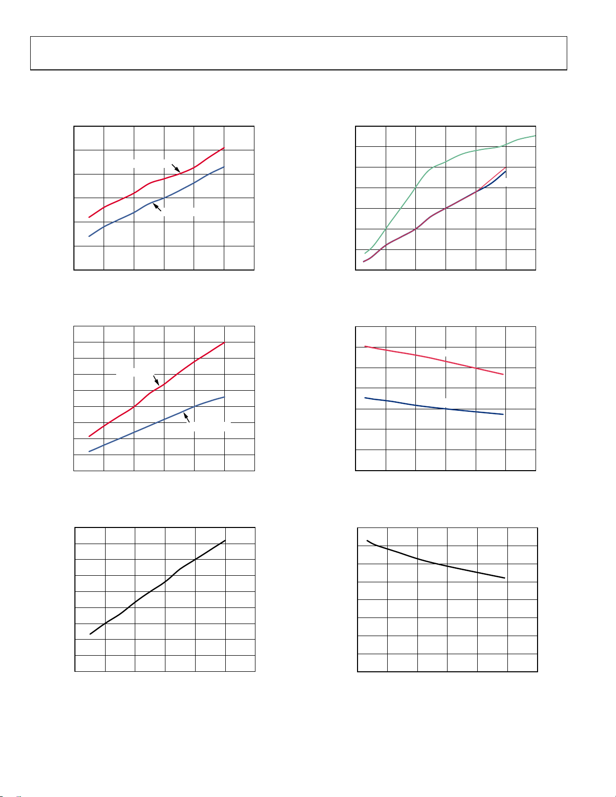
TYPICAL PERFORMANCE CHARACTERISTICS
f
= 122.88 MHz, REFA differential at 30.72 MHz, f
VCXO
60
50
40
30
CURRENT (mA)
20
HSTL = 16mA
HSTL = 8mA
= 3686.4 MHz, and doubler is off, unless otherwise noted.
VCO
35
30
25
20
15
CURRENT (mA)
10
20pF
10pF
2pF
10
0
0 200 400 600 800 1000 1200
FREQUENCY ( MHz)
08439-003
Figure 3. VDD3_OUT[x:y] Current (Typical) vs. Frequency;
HSTL Mode, 16 mA and 8 mA
45
40
35
30
25
20
CURRENT (mA)
15
10
5
0
0 200 400 600 800 1000 1200
LVD S = 7 mA
LVDS = 3.5mA
08439-004
FREQUENCY ( MHz)
Figure 4. VDD3_OUT[x:y] Current (Typical) vs. Frequency;
LVDS Mode, 7 mA and 3.5 mA
45
40
35
30
25
20
CURRENT (mA)
15
10
5
0
0 200 400 600 800 1000 1200
FREQUENCY ( MHz)
08439-005
Figure 5. VDD3_OUT[x:y] Current (Typical) vs. Frequency, LVPECL Mode
5
0
0 100 200 300 400 500 600
FREQUENCY ( MHz)
08439-006
Figure 6. VDD3_OUT[x:y] Current (Typical) vs. Frequency;
CMOS Mode, 20 pF, 10 pF, and 2 pF Load
3.5
3.0
2.5
2.0
L SWING (V p-p)
1.5
1.0
DIFFERENTI
0.5
0
0 200 400 600 800 1000 1200
HSTL = 16mA
HSTL = 8mA
FREQUENCY ( MHz)
08439-007
Figure 7. Differential Voltage Swing vs. Frequency;
HSTL Mode, 16 mA and 8 mA
1.6
1.4
1.2
1.0
0.8
0.6
0.4
DIFFERENTIAL SWING (V p-p)
0.2
0
0 200 400 600 800 1000 1200
FREQUENCY (MHz)
08439-008
Figure 8. Differential Voltage Swing vs. Frequency,
LVPECL Mode
Rev. B | Page 16 of 56
AD9523
A
–
–
1.4
1.2
LVD S = 7 m A
1.0
0.8
L SWING (V p-p )
0.6
LVD S = 3 . 5m A
0.4
DIFFERENTI
0.2
0
0 200 400 600 800 1000 1200
FREQUENCY ( MHz)
Figure 9. Differential Voltage Swing vs. Frequency;
LVDS Mode, 7 mA and 3.5 mA
08439-009
70
–80
1
–90
–100
–110
–120
–130
–140
PHASE NOISE (dBc/Hz)
–150
–160
–170
100 1k 10k 100k 1M 10M
2
3
4
NOISE:
ANALYSIS RANG E X: BAND M ARKER
ANALYSIS RANG E Y: BAND M ARKER
INTG NOISE: –75.94595dBc/39.99MHz
RMS NOISE: 225.539µRAD
12.9224mdeg
RMS JITTER: 194.746fsec
RESIDUAL FM: 2.81623kHz
1: 100Hz, –85.0688dBc/Hz
2: 1kHz, –113.3955dBc/Hz
3: 8kHz, –125.8719dBc/Hz
4: 16kHz, –129.5942dBc/Hz
5: 100kHz, –134.5017dBc/Hz
6: 1MHz, –145.2872dBc/Hz
7: 10MHz, –156.2706dBc/Hz
8: 40MHz, –157.4153dBc/Hz
x: START 12kHz
CENTER 40.006MHz
SPAN 79.988MHz
5
FREQUENCY (Hz)
Figure 12. Phase Noise, Output = 184.32 MHz
(VCXO = 122.88 MHz, Crystek VCXO CVHD-950)
STOP 80MHz
6
7
8
08439-015
4.0
3.5
3.0
2.5
2pF
10pF
20pF
2.0
1.5
AMPLITUDE (V)
1.0
0.5
0
0 100 200 300 400 500 600
FREQUENCY ( MHz)
Figure 10. Amplitude vs. Frequency and Capacitive Load;
CMOS Mode, 2 pF, 10 pF, and 20 pF
1
70
–80
1
–90
–100
–110
–120
–130
–140
PHASE NOISE (dBc/Hz)
–150
–160
08439-010
–170
100 1k 10k 100k 1M 10M
2
3
NOISE:
ANALYSIS RANG E X: BAND M ARKER
ANALYSIS RANG E Y: BAND M ARKER
INTG NOISE: –78.8099dBc/39.99MHz
RMS NOISE: 162.189µRAD
9.29276mdeg
RMS JITTER: 210.069fsec
RESIDUAL FM: 2.27638kHz
4
FREQUENCY (Hz)
1: 100Hz, –89.0260dBc/Hz
2: 1kHz, –116.9949dBc/Hz
3: 8kHz, –129.5198dBc/Hz
4: 16kHz, –133.3916dBc/Hz
5: 100kHz, –137.7680dBc/Hz
6: 1MHz, –148.3519dBc/Hz
7: 10MHz, –158.3307dBc/Hz
8: 40MHz, 159.1629–dBc/Hz
x: START 12kHz
STOP 80MHz
CENTER 40.006MHz
SPAN 79.988MHz
5
6
7
8
08439-016
Figure 13. Phase Noise, Output = 122.88 MHz
(VCXO = 122.88 MHz, Crystek VCXO CVHD-950; Doubler Is Off)
1
CH1 200mV 2.5ns/DI V
40.0GS/s
A CH1 104mV
Figure 11. Output Waveform (Differential), LVPECL at 122.88 MHz
08439-013
CH1 500mV Ω 2.5ns/DIV
40.0GS/s
A CH1 80mV
08439-049
Figure 14. Output Waveform (Differential), HSTL at 16 mA, 122.88 MHz
Rev. B | Page 17 of 56

AD9523
INPUT/OUTPUT TERMINATION RECOMMENDATIONS
AD9523
LVD S
OUTPUT
0.1µF
100Ω
0.1µF
HIGH
IMPEDANCE
INPUT
DOWNSTREAM
Figure 15. AC-Coupled LVDS Output Driver
AD9523
LVD S
OUTPUT
100Ω
HIGH
IMPEDANCE
INPUT
DOWNSTREAM
Figure 16. DC-Coupled LVDS Output Driver
AD9523
LVPECL-
COMPATIBLE
OUTPUT
0.1µF
100Ω
0.1µF
HIGH
IMPEDANCE
INPUT
DOWNSTREAM
Figure 17. AC-Coupled LVPECL Output Driver
DEVICE
DEVICE
DEVICE
AD9523
HSTL
OUTPUT
08439-142
0.1µF
100Ω
0.1µF
HIGH
IMPEDANCE
INPUT
DOWNSTRE AM
DEVICE
08439-046
Figure 19. AC-Coupled HSTL Output Driver
AD9523
HSTL
OUTPUT
08439-143
100Ω
HIGH
IMPEDANCE
INPUT
DOWNSTREAM
DEVICE
08439-047
Figure 20. DC-Coupled HSTL Output Driver
AD9523
0.1µF
0.1µF
SELF-BIASED
REF, VCXO,
ZERO DEL AY
INPUTS
08439-048
100Ω
1
(OPTIONAL
08439-044
1
)
RESISTOR VALUE DEPENDS UPON
REQUIRED TERMINATION OF S OURCE.
Figure 21. REF, VCXO, and Zero Delay Input Differential Mode
AD9523
LVPECL
COMPATIBLE
OUTPUT
100Ω
HIGH
IMPEDANCE
INPUT
DOWNSTREAM
DEVICE
08439-045
Figure 18. DC-Coupled LVPECL Output Driver
Rev. B | Page 18 of 56

AD9523
TERMINOLOGY
Phase Jitter and Phase Noise
An ideal sine wave can be thought of as having a continuous
and even progression of phase with time from 0° to 360° for
each cycle. Actual signals, however, display a certain amount
of variation from ideal phase progression over time. This
phenomenon is called phase jitter. Although many causes can
contribute to phase jitter, one major cause is random noise,
which is characterized statistically as being Gaussian (normal)
in distribution.
This phase jitter leads to a spreading out of the energy of the
sine wave in the frequency domain, producing a continuous
power spectrum. This power spectrum is usually reported as a
series of values whose units are dBc/Hz at a given offset in
frequency from the sine wave (carrier). The value is a ratio
(expressed in decibels) of the power contained within a 1 Hz
bandwidth with respect to the power at the carrier frequency.
For each measurement, the offset from the carrier frequency is
also given.
It is meaningful to integrate the total power contained within
some interval of offset frequencies (for example, 10 kHz to
10 MHz). This is called the integrated phase noise over that
frequency offset interval and can be readily related to the time
jitter due to the phase noise within that offset frequency interval.
Phase noise has a detrimental effect on the performance of ADCs,
DACs, and RF mixers. It lowers the achievable dynamic range of
the converters and mixers, although they are affected in somewhat
different ways.
Time Jitter
Phase noise is a frequency domain phenomenon. In the time
domain, the same effect is exhibited as time jitter. When observing
a sine wave, the time of successive zero crossings varies. In a square
wave, the time jitter is a displacement of the edges from their
ideal (regular) times of occurrence. In both cases, the variations in
timing from the ideal are the time jitter. Because these variations
are random in nature, the time jitter is specified in seconds root
mean square (rms) or 1 sigma (Σ) of the Gaussian distribution.
Time jitter that occurs on a sampling clock for a DAC or an
ADC decreases the signal-to-noise ratio (SNR) and dynamic
range of the converter. A sampling clock with the lowest possible
jitter provides the highest performance from a given converter.
Additive Phase Noise
Additive phase noise is the amount of phase noise that can be
attributed to the device or subsystem being measured. The phase
noise of any external oscillators or clock sources is subtracted.
This makes it possible to predict the degree to which the device
impacts the total system phase noise when used in conjunction
with the various oscillators and clock sources, each of which
contributes its own phase noise to the total. In many cases, the
phase noise of one element dominates the system phase noise.
When there are multiple contributors to phase noise, the total is
the square root of the sum of squares of the individual contributors.
Additive Time Jitter
Additive time jitter is the amount of time jitter that can be
attributed to the device or subsystem being measured. The time
jitter of any external oscillators or clock sources is subtracted.
This makes it possible to predict the degree to which the device
impacts the total system time jitter when used in conjunction with
the various oscillators and clock sources, each of which contributes
its own time jitter to the total. In many cases, the time jitter of the
external oscillators and clock sources dominates the system time
jitter.
Rev. B | Page 19 of 56

AD9523
THEORY OF OPERATION
DETAILED BLOCK DIAGRAM
VCXO
STATUS0/
VDD3_PLL1
LDO_PLL1 LDO_VCO
OSC_CTRL OSC_IN
PLL1_OUT
SP0
STATUS1/
SP1
LF2_EXT_CAPLF1_EXT_CAP
VDD1.8_O UT[x:y]
VDD3_OUT[ x:y]
REFA
REFA
REF_SEL
REFB
REFB
REF_TEST
SDIO/SDA
SDO
SCLK/SCL
RESET
EEPROM_SEL
÷R
SWITCH-
OVER
CONTROL
÷R
÷R
CONTROL
CS
PD
INTERFACE
(SDI AND I
EEPROM
2
C)
÷N1
LOCK
DETECT
P
F
D
LOOP
FILTER
CHARGE
PUMP
PLL1
AD9523
LDO_PLL2
Figure 22. Top Level Diagram
OVERVIEW
The AD9523 is a clock generator that employs integer-N-based
phase-locked loops (PLL). The device architecture consists of
two cascaded PLL stages. The first stage, PLL1, consists of an
integer division PLL that uses an external voltage-controlled
crystal oscillator (VCXO) from 15 MHz to 250 MHz. PLL1 has
a narrow-loop bandwidth that provides initial jitter cleanup of the
input reference signal. The second stage, PLL2, is a frequency
multiplying PLL that translates the first stage output frequency
to a range of 3.6 GHz to 4.0 GHz. PLL2 incorporates an integerbased feedback divider that enables integer frequency multiplication. Programmable integer dividers (1 to 1024) follow PLL2,
establishing a final output frequency of 1 GHz or less.
The AD9523 includes reference signal processing blocks that
enable a smooth switching transition between two reference
inputs. This circuitry automatically detects the presence of the
reference input signals. If only one input is present, the device
uses it as the active reference. If both are present, one becomes
the active reference and the other becomes the backup reference.
If the active reference fails, the circuitry automatically switches
to the backup reference (if available), making it the new active
reference. A register setting determines what action to take
Rev. B | Page 20 of 56
÷D1
×2
STATUS MO NITOR
LOCK DETECT/
SERIAL PORT
ADDRESS
LOCK
DETECT
P
CHARGE
F
PUMP
D
÷N2
VDD3_PLL2 VDD1.8_PLL2
LOOP
FILTER
VCO
SYNC
SIGNAL
÷M1
PLL2
TO SYNC
SYNC
∆t
÷D
EDGE
∆t
÷D
EDGE
∆t
÷D
EDGE
∆t
÷D
EDGE
∆t
÷D
EDGE
∆t
÷D
EDGE
∆t
÷D
EDGE
∆t
÷D
EDGE
∆t
÷D
EDGE
∆t
÷D
EDGE
∆t
÷D
EDGE
∆t
÷D
EDGE
∆t
÷D
EDGE
∆t
÷D
EDGE
OUT13
OUT13
OUT12
OUT12
OUT11
OUT11
OUT10
OUT10
OUT9
OUT9
OUT8
OUT8
OUT7
OUT7
OUT6
OUT6
OUT5
OUT5
OUT4
OUT4
OUT3
OUT3
OUT2
OUT2
OUT1
OUT1
OUT0
OUT0
ZD_IN
ZD_IN
if the failed reference is once again available: either stay on
Reference B or revert to Reference A. If neither reference can
be used, the AD9523 supports a holdover mode. A reference
select pin (REF_SEL, Pin 16) is available to manually select
which input reference is active (see Table 4 2). The accuracy of the
holdover is dependent on the external VCXO frequency
stability at half supply voltage.
Any of the divider settings are programmable via the serial
programming port, enabling a wide range of input/output
frequency ratios under program control. The dividers also
include a programmable delay to adjust timing of the output
signals, if required.
The output is compatible with LVPECL, LVDS, or HSTL logic
levels (see the Input/Output Termination Recommendations
section); however, the AD9523 is implemented only in CMOS.
The loop filters of each PLL are integrated and programmable.
Only a single external capacitor for each of the two PLL loop
filters is required.
The AD9523 operates over the extended industrial temperature
range of −40°C to +85°C.
08439-020

AD9523
COMPONENT BLOCKS—INPUT PLL (PLL1)
PLL1 General Description
Fundamentally, the input PLL (referred to as PLL1) consists of
a phase-frequency detector (PFD), charge pump, passive loop
filter, and an external VCXO operating in a closed loop.
PLL1 has the flexibility to operate with a loop bandwidth of
approximately 10 Hz to 100 Hz. This relatively narrow loop
bandwidth gives the AD9523 the ability to suppress jitter that
appears on the input references (REFA and REFB). The output
of PLL1 then becomes a low jitter phase-locked version of the
reference input system clock.
PLL1 Reference Clock Inputs
The AD9523 features two separate differential reference clock
inputs, REFA and REFB. These inputs can be configured to
operate in full differential mode or single-ended CMOS mode.
In differential mode, these pins are internally self-biased. If
REFA
REFA or REFB is driven single-ended, the unused side (
REFB
) should be decoupled via a suitable capacitor to a quiet
ground. shows the equivalent circuit of REFA or REFB.
Figure 21
It is possible to dc-couple to these inputs, but the dc operation
point should be set as specified in the tables.
Specifications
To operate either the REFA or the REFB inputs in 3.3 V CMOS
mode, the user must set Bit 5 or Bit 6, respectively, in Register
0x01A (see Tabl e 4 0 ). The single-ended inputs can be driven by
either a dc-coupled CMOS level signal or an ac-coupled sine
wave or square wave.
The differential reference input receiver is powered down when
the differential reference input is not selected, or when the PLL
is powered down. The single-ended buffers power down when
the PLL is powered down, when their respective individual powerdown registers are set, or when the differential receiver is selected.
The REFB R divider uses the same value as the REFA R divider
unless Bit 7, the enable REFB R divider independent division
control bit in Register 0x01C, is programmed as shown in Tab le 4 2 .
,
PLL1 Loop Filter
The PLL1 loop filter requires the connection of an external
capacitor from LF1_EXT_CAP (Pin 7) to ground. The value of the
external capacitor depends on the use of an external VCXO, as
well as such configuration parameters as input clock rate and
desired bandwidth. Normally, a 0.3 µF capacitor allows the loop
bandwidth to range from 10 Hz to 100 Hz and ensures loop
stability over the intended operating parameters of the device
(see Tabl e 43 for R
AD9523
R
ZERO
CHARGE
PUMP
values).
ZERO
LF1_EXT_CAP LDO_PLL1
C
POLE1
C
R
POLE2
POLE2
Figure 23. PLL1 Loop Filter
BUFFER
OSC_CTRL
1kΩ
0.3µF
Table 19. PLL1 Loop Filter Programmable Values
R
C
R
C
ZERO
(kΩ)
POLE1
(nF)
POLE2
(kΩ)
POLE2
(nF)
LF1_EXT_CAP1
(μF)
883 1.5 fixed 165 fixed 0.337 fixed 0.3
677
341
135
10
External
1
External loop filter capacitor.
An external R-C low-pass filter should be used at the OSC_CTRL
output. The values shown in Figure 23 add an additional low-pass
pole at ~530 Hz. This R-C network filters the noise associated
with the OSC_CTRL buffer to achieve the best noise performance
at the 1 kHz offset region.
08439-022
LF1_EXT_CAP
REFA
REFA
REF_SEL
REFB
REFB
REF_TEST
DIVIDE- BY1, 2, .. .1023
SWITCH-
OVER
DIVIDE- BY1, 2, .. .1023
3.3V CMOS
OR 1.8V
DIFFERENTIAL
DIVIDE-BY-
1, 2, ...63
1.8V LDO
VDD3_PLL LDO_PLL1
CONTROL
P
D
Figure 24. Input PLL (PLL1) Block Diagram
Rev. B | Page 21 of 56
F
0.5µA LSB
R
ZERO
CHARGE
PUMP
7 BITS,
C
POLE1
DIVIDE- BY-
1, 2, .. .1023
R
POLE2
C
POLE2
AD9523
OSC_CTRL
VCXO
OSC_IN
08439-021

AD9523
PLL1 Input Dividers
Each reference input feeds a dedicated reference divider block.
The input dividers provide division of the reference frequency
in integer steps from 1 to 1023. They provide the bulk of the
frequency prescaling that is necessary to reduce the reference
frequency to accommodate the bandwidth that is typically
desired for PLL1.
PLL1 Reference Switchover
The reference monitor verifies the presence/absence of the
prescaled REFA and REFB signals (that is, after division by the
input dividers). The status of the reference monitor guides the
activity of the switchover control logic. The AD9523 supports
automatic and manual PLL reference clock switching between
REFA (the REFA and
REFB
pins). This feature supports networking and infrastructure
REFA
pins) and REFB (the REFB and
applications that require redundant references.
There are several configurable modes of reference switchover.
The manual switchover is achieved either via a program-ming
register setting or by using the REF_SEL pin. The automatic
switchover occurs when REFA disappears and there is a reference
on REFB.
The reference automatic switchover can be set to work as follows:
• Nonrevertive: stay on REFB. Switch from REFA to REFB
when REFA disappears, but do not switch back to REFA
if it reappears. If REFB disappears, then go back to REFA.
• Revert to REFA. Switch from REFA to REFB when REFA
disappears. Return to REFA from REFB when REFA returns.
See Tab le 4 2 for the PLL1 miscellaneous control register bit
settings.
PLL1 Holdover
In the absence of both input references, the device enters
holdover mode. Holdover is a secondary function that is
provided by PLL1. Because PLL1 has an external VCXO
available as a frequency source, it continues to operate in the
absence of the input reference signals. When the device
switches to holdover, the charge pump tristates. The device
continues operating in this mode until a reference signal
becomes available. Then the device exits holdover mode,
and PLL1 resynchronizes with the active reference. In addition
to tristate, the charge pump can be forced to VCC/2 during
holdover (see Ta b l e 42, Bit 6 in Register 0x01C).
COMPONENT BLOCKS—OUTPUT PLL (PLL2)
PLL2 General Description
The output PLL (referred to as PLL2) consists of an optional
input reference doubler, phase-frequency detector (PFD),
a partially integrated analog loop filter (see Figure 25), an
integrated voltage-controlled oscillator (VCO), and a feedback
divider. The VCO produces a nominal 3.8 GHz signal with an
output divider that is capable of division ratios of 4 to 11.
The PFD of the output PLL drives a charge pump that increases,
decreases, or holds constant the charge stored on the loop filter
capacitors (both internal and external). The stored charge
results in a voltage that sets the output frequency of the VCO.
The feedback loop of the PLL causes the VCO control voltage to
vary in a way that phase locks the PFD input signals.
The gain of PLL2 is proportional to the current delivered by the
charge pump. The loop filter bandwidth is chosen to reduce
noise contributions from PLL sources that could degrade phase
noise requirements.
The output PLL has a VCO with multiple bands spanning a
range of 3.6 GHz to 4.0 GHz. However, the actual operating
frequency within a particular band depends on the control
voltage that appears on the loop filter capacitor. The control
voltage causes the VCO output frequency to vary linearly within
the selected band. This frequency variability allows the control
loop of the output PLL to synchronize the VCO output signal
with the reference signal applied to the PFD. Typically, the
device automatically selects the appropriate band as part of its
calibration process (invoked via the VCO control register at
Address 0x0F3).
PLL1_OUT
AD9523
DIVIDE BY
1, 2, 4, 8, 16
×2
PFD
LF2_EXT_CAP
R
ZERO
CHARGE PUMP
8 BITS, 3. 5µA LSB
A/B
COUNTER S
Figure 25. Output PLL (PLL2) Block Diagram
Rev. B | Page 22 of 56
LDO_VCO
C
POLE1
N DIVIDER
C
POLE2
R
POLE2
DIVIDE-BY-4
PRESCALER
LDO
LDO
PLL_1.8V
DIVIDE BY
4, 5, 6, .. .11
LDO_PLL2VDD3_PLL2
TO DIST/
RESYNC
08439-023

AD9523
Input 2× Frequency Multiplier
The 2× frequency multiplier provides the option to double
the frequency at the PLL2 input. This allows the user to take
advantage of a higher frequency at the input to the PLL (PFD)
and, thus, allows for reduced in-band phase noise and greater
separation between the frequency generated by the PLL and the
modulation spur associated with PFD. However, increased
reference spur separation results in harmonic spurs introduced
by the frequency multiplier that increase as the duty cycle
deviates from 50% at the OSC_IN inputs. As such, beneficial
use of the frequency multiplier is application-specific. Typically,
a VCXO with proper interfacing has a duty cycle that is
approximately 50% at the OSC_IN inputs. Note that the
maximum output frequency of the 2× frequency multipliers
must not exceed the maximum PFD rate that is specified in
Tabl e 11 .
PLL2 Feedback Divider
PLL2 has a feedback divider (N divider) that enables it to provide
integer frequency up-conversion.
bination of a prescaler (P) and two counters, A and B.
divider value is
The PLL2 N divider is a com-
The total
N = (P × B) + A
where P = 4.
The feedback divider is a dual modulus prescaler architecture, with
a nonprogrammable P that is equal to 4. The value of the B counter
can be from 4 to 63, and the value of the A counter can be from 0 to 3.
However, due to the architecture of the divider, there are constraints,
as listed in
Tabl e 45 .
PLL2 Loop Filter
The PLL2 loop filter requires the connection of an external
capacitor from LF2_EXT_CAP (Pin 11) to LDO_VCO (Pin 14),
as illustrated in Figure 25. The value of the external capacitor
depends on the operating mode and the desired phase noise
performance. For example, a loop bandwidth of approximately
500 kHz produces the lowest integrated jitter. A lower bandwidth
produces lower phase noise at 1 MHz but increases the total
integrated jitter.
Table 20. PLL2 Loop Filter Programmable Values
R
C
R
C
ZERO
(Ω)
3250 48 900 Fixed at 16 Typical at 1000
3000 40 450
2750 32 300
2500 24 225
2250 16
2100 8
2000 0
1850
1
External loop filter capacitor.
POLE1
(pF)
POLE2
(Ω)
POLE2
(pF)
LF2_EXT_CAP1
(pF)
VCO Divider
The VCO divider provides frequency division between the
internal VCO and the clock distribution. The VCO divider can
be set to divide by 4, 5, 6, 7, 8, 9, 10, or 11.
VCO Calibration
The AD9523 on-chip VCO must be manually calibrated to ensure
proper operation over process and temperature. This is accomplished by setting the calibrate VCO bit (Register 0x0F3, Bit 1) to 1.
(This bit is not self-clearing.) The setting can be performed
as part of the initial setup before executing the IO_Update bit
(Register 0x234, Bit 0 = 1). A readback bit, VCO calibration in
progress (Register 0x22D, Bit 0), indicates when a VCO
calibration is in progress by returning a logic true (that is, Bit 0 = 1).
If the EEPROM is in use, setting the calibrate VCO bit to 1 before
saving the register settings to the EEPROM ensures that the VCO
calibrates automatically after the EEPROM has loaded. After
calibration, it is recommended that a sync be initiated (see the
Clock Distribution Synchronization section).
Note that the calibrate VCO bit defaults to 0. This bit must
change from 0 to 1 to initiate a calibration sequence. Therefore,
any subsequent calibrations require the following sequence:
1. Register 0x0F3, Bit 1 (calibrate VCO bit) = 0
2. Register 0x234, Bit 0 (IO_Update bit) = 1
3. Register 0x0F3, Bit 1 (calibrate VCO bit) = 1
4. Register 0x234, Bit 0 (IO_Update bit) = 1
VCO calibration is controlled by a calibration controller that
runs off the VCXO input clock. The calibration requires that
PLL2 be set up properly to lock the PLL2 loop and that the
VCXO clock be present.
During power-up or reset, the distribution section is automatically
held in sync until the first VCO calibration is finished. Therefore,
no outputs can occur until VCO calibration is complete and PLL2
is locked.
Initiate a VCO calibration under the following conditions:
• After changing any of the PLL2 B counter and A counter
settings or after a change in the PLL2 reference clock
frequency. This means that a VCO calibration should be
initiated any time that a PLL2 register or reference clock
changes such that a different VCO frequency is the result.
• Whenever system calibration is desired. The VCO is designed
to operate properly over extremes of temperature even
when it is first calibrated at the opposite extreme. However,
a VCO calibration can be initiated at any time, if desired.
Rev. B | Page 23 of 56

AD9523
V
CLOCK DISTRIBUTION
The clock distribution block provides an integrated solution for
generating multiple clock outputs based on frequency dividing
the PLL2 VCO divider output. The distribution output consists
of 14 channels (OUT0 to OUT13). Each of the output channels
has a dedicated divider and output driver, as shown in Figure 25.
The AD9523 also has the capability to route the VCXO output
to four of the outputs (OUT0 to OUT3).
Clock Dividers
The output clock distribution dividers are referred to as D0 to
D13, corresponding to output channels OUT0 through OUT13,
respectively. Each divider is programmable with 10 bits of division
depth that is equal to 1 to 1024. Dividers have duty cycle correction
to always give 50% duty cycle, even for odd divides.
Output Power-Down
Each of the output channels offers independent control of the
power-down functionality via the Channel 0 to Channel 13 control
registers (see Ta b le 5 0). Each output channel has a dedicated
power-down bit for powering down the output driver. However,
if all 14 outputs are powered down, the entire distribution output
enters a deep sleep mode. Although each channel has a channel
power-down control signal, it may sometimes be desirable to
power down an output driver while maintaining the divider’s
synchronization with the other channel dividers. This is accomplished by placing the output in tristate mode (this works in
CMOS mode, as well).
Multimode Output Drivers
The user has independent control of the operating mode of each of
the fourteen output channels via the Channel 0 to Channel 13
control registers (see Tabl e 50 ). The operating mode control
includes the following:
• Logic family and pin functionality
• Output drive strength
• Output polarity
If the output channel is ac-coupled to the circuit to be clocked,
changing the mode varies the voltage swing to determine sensitivity to the drive level. For example, in LVDS mode, a current of
3.5 mA causes a 350 mV peak voltage. Likewise, in LVPECL mode,
a current of 8 mA causes an 800 mV peak voltage at the 100 Ω load
resistor.
In addition to the four mode bits, each of the 14 Channel 0 to
Channel 13 control registers includes the following control bits:
• Invert divider output. Enables the user to choose between
normal polarity and inverted polarity. Normal polarity is the
default state. Inverted polarity reverses the representation of
Logic 0 and Logic 1, regardless of the logic family.
• Ignore sync. Makes the divider ignore the
SYNC
signal
from any source.
• Power down channel. Powers down the entire channel.
• Lower power mode.
• Driver mode.
• Channel divider.
• Divider phase.
DD3_OUT[x:y]
1.25V LVDS
VDD – 1.3V LVPECL
CM
COMMON-MODE
CIRCUIT
P
CM
+–
100Ω LOAD
N
50Ω
HSTL
ENABLED
N
P
The four least significant bits (LSBs) of each of the 14 Channel 0
to Channel 13 control registers comprise the driver mode bits. The
mode value selects the desired logic family and pin functionality
3.5mA/8mA
LVDS/LVPECL
ENABLED
50Ω
HSTL
ENABLED
of an output channel, as listed in Tab le 5 0. This driver design
allows a common 100 Ω external resistor for all the different
driver modes of operation that are illustrated in Figure 26.
Rev. B | Page 24 of 56
Figure 26. Multimode Driver
08439-031

AD9523
Clock Distribution Synchronization
A block diagram of the clock distribution synchronization
functionality is shown in Figure 27. The synchronization
sequence begins with the primary synchronization signal,
which ultimately results in delivery of a synchronization strobe
to the clock distribution logic.
As indicated, the primary synchronization signal originates
from one of the following sources:
• Direct synchronization source via the sync dividers bit (see
Register 0x232, Bit 0 in Tab le 5 4)
• Device pin,
SYNC
(Pin 17)
An automatic synchronization of the divider is initiated the first
time that PLL2 locks after a power-up or reset event. Subsequent
lock/unlock events do not initiate a resynchronization of the
distribution dividers unless they are preceded by a power-down
or reset of the part.
Both sources of the primary synchronization signal are logic OR’d;
therefore, any one of them can synchronize the clock distribution
output at any time. When using the sync dividers bit, the user
first sets and then clears the bit. The synchronization event is the
clearing operation (that is, the Logic 1 to Logic 0 transition of
the bit). The dividers are all automatically synchronized to each
other when PLL2 is ready. The dividers support programmable
phase offsets from 0 to 63 steps, in half periods of the input
clock (for example, the VCO divider output clock). The phase
offsets are incorporated in the dividers through a preset for the
first output clock period of each divider. Phase offsets are supported only by programming the initial phase and divide value
and then issuing a sync to the distribution (automatically at startup
or manually, if desired).
In normal operation, the phase offsets are already programmed
through the EEPROM or the SPI/I
2
C port before the AD9523
starts to provide outputs. Although the user cannot adjust the
phase offsets while the dividers are operating, it is possible to
adjust the phase of all the outputs together without powering
down PLL1 and PLL2. This is accomplished by programming
the new phase offset, using Bits[7:2] in Register 0x192 (see
Tabl e 50 ) and then issuing a divide sync signal by using the
SYNC
pin or the sync dividers bit (Register 0x232, Bit 0).
DIVIDE
PHASE
SYNC
DIVIDER
OUT
DRIVER
OUTx
OUTx
VCO OUTPUT DIVIDER
FAN OUT
SYNC (PIN 17)
SYNC DIVIDERS BI T
Figure 27. Clock Output Synchronization Block Diagram
SYNC
08439-025
SYNC
VCO DIVIDER OUT PUT CLOCK
DIVIDE = 2, PHASE = 0
DIVIDE = 2, PHASE = 6
CONTROL
6 × 0.5 PERIODS
Figure 28. Clock Output Synchronization Timing Diagram
8439-026
Rev. B | Page 25 of 56

AD9523
All outputs that are not programmed to ignore the sync
are disabled temporarily while the sync is active. Note that,
if an output is used for the zero delay path, it also disappears
momentarily. However, this is desirable because it ensures that
all the synchronized outputs have a deterministic phase
relation-ship with respect to the zero delay output and,
therefore, also with respect to the input.
ZERO DELAY OPERATION
Zero delay operation aligns the phase of the output clocks with
the phase of the external PLL reference input. The OUT0 output
is designed to be used as the output for zero delay. There are
two zero delay modes on the AD9523: internal and external
(see Figure 29). Note that the external delay mode provides
better matching than the internal delay mode because the
output drivers are included in the zero delay path. Setting the
anitbacklash pulse width control of PLL1 to maximum gives the
best zero delay matching.
Internal Zero Delay Mode
The internal zero delay function of the AD9523 is achieved by
feeding the output of Channel Divider 0 back to the PLL1 N
divider. Bit 5 in Register 0x01B is used to select internal zero delay
mode (see Tabl e 4 1 ). In the internal zero delay mode, the output
of Channel Divider 0 is routed back to the PLL1 (N divider)
through a mux. PLL1 synchronizes the phase/edge of the output
of Channel Divider 0 with the phase/edge of the reference input.
Because the channel dividers are synchronized to each other,
the outputs of the channel divider are synchronous with the
reference input.
External Zero Delay Mode
The external zero delay function of the AD9523 is achieved by
feeding OUT0 back to the ZD_IN input and, ultimately, back to
the PLL1 N divider. In Figure 29, the change in signal routing
for external zero delay is external to the AD9523.
Bit 5 in Register 0x01B is used to select the external zero delay
mode. In external zero delay mode, OUT0 must be routed back to
PLL1 (the N divider) through the ZD_IN and
ZD_IN
pins.
PLL1 synchronizes the phase/edge of the feedback output clock
with the phase/edge of the reference input. Because the channel
dividers are synchronized to each other, the clock outputs are
synchronous with the reference input. Both the reference path
delay and the feedback delay from ZD_IN are designed to have
the same propagation delay from the output drivers and PLL
components to minimize the phase offset between the clock
output and the reference input to achieve zero delay.
REFA
REFA
ZD_IN
FEEDBACK
DELAY
REF
DELAY
INTERNAL FB
PFD
OUT0OUT0ZD_IN
ENB
AD9523
Figure 29. Zero Delay Function
08439-027
Rev. B | Page 26 of 56

AD9523
A
SERIAL CONTROL PORT
The AD9523 serial control port is a flexible, synchronous serial
communications port that allows an easy interface with many
industry-standard microcontrollers and microprocessors. The
AD9523 serial control port is compatible with most synchronous
transfer formats, including Philips IC®, Motorola® SPI, and
Intel® SSR protocols. The AD9523 IC implementation deviates
from the classic IC specification in two specifications, and
these deviations are documented in Tabl e 1 5 of this data sheet.
The serial control port allows read/write access to all registers
that configure the AD9523.
SPI/I²C PORT SELECTION
The AD9523 has two serial interfaces, SPI and IC. Users can
select either the SPI or IC depending on the states (logic high,
logic low) of the two logic level input pins, SP1 and SP0, when
power is applied or after a
40 kΩ pull-down resistor).
the SPI interface is active. Otherwise, I
2
different I
in . The five MSBs of the slave address are hardware
Tabl e 21
C slave address settings (seven bits wide), as shown
RESET
(each pin has an internal
When both SP1 and SP0 are low,
2
C is active with three
coded as 11000, and the two LSBs are determined by the logic
levels of the SP1 and SP0 pins.
Table 21. Serial Port Mode Selection
SP1 SP0 Address
Low Low SPI
Low High I2C: 1100000
High Low I2C: 1100001
High High I2C: 1100010
I²C SERIAL PORT OPERATION
The AD9523 IC port is based on the IC fast mode standard.
The AD9523 supports both IC protocols: standard mode
(100 kHz) and fast mode (400 kHz).
The AD9523 IC port has a 2-wire interface consisting of a serial
data line (SDA) and a serial clock line (SCL). In an IC bus system,
the AD9523 is connected to the serial bus (data bus SDA and
clock bus SCL) as a slave device, meaning that no clock is generated
by the AD9523. The AD9523 uses direct 16-bit (two bytes)
memory addressing instead of traditional 8-bit (one byte) memory
addressing.
I2C Bus Characteristics
Table 22. I2C Bus Definitions
Abbreviation Definition
S Start
Sr Repeated start
P
A
A
W
Stop
Acknowledge
No acknowledge
Write
R Read
One pulse on the SCL clock line is generated for each data bit
that is transferred.
The data on the SDA line must not change during the high period
of the clock. The state of the data line can change only when the
clock on the SCL line is low.
SDA
SCL
DATA LINE
STABLE;
DATA VALID
Figure 30. Valid Bit Transfer
CHANGE
OF DATA
ALLOWED
A start condition is a transition from high to low on the SDA
line while SCL is high. The start condition is always generated
by the master to initialize the data transfer.
A stop condition is a transition from low to high on the SDA
line while SCL is high. The stop condition is always generated
by the master to end the data transfer.
SD
SCL
S
START
CONDITION
Figure 31. Start and Stop Conditions
P
STOP
CONDITIO N
A byte on the SDA line is always eight bits long. An acknowledge
bit must follow every byte. Bytes are sent MSB first.
The acknowledge bit is the ninth bit attached to any 8-bit data
byte. An acknowledge bit is always generated by the receiving
device (receiver) to inform the transmitter that the byte has
been received. It is accomplished by pulling the SDA line low
during the ninth clock pulse after each 8-bit data byte.
8439-160
08439-161
Rev. B | Page 27 of 56

AD9523
SDA
SDA
SDA
MSB
ACKNOWLEDGE FROM
SLAVE-RECEIV ER
ACKNOWLEDGE FROM
SLAVE-RECEIVER
SCL
SCL
SCL
S
S
S
1 2 8 9 1 2 83 TO 73 TO 7 9 10
Figure 32. Acknowledge Bit
MSB = 0
ACKNOWLEDGE FROM
SLAVE-RECEIV ER
1 2 8 9 1 2 83 TO 73 TO 7 9 10
Figure 33. Data Transfer Process (Master Write Mode, 2-Byte Transfer Used for Illustration)
MSB = 1
ACKNOWLEDGE FROM
MASTER-RECEIVER
1 2 8 9 1 2 83 TO 73 TO 7 9 10
Figure 34. Data Transfer Process (Master Read Mode, 2-Byte Transfer Used for Illustration)
The no acknowledge bit is the ninth bit attached to any 8-bit
data byte. A no acknowledge bit is always generated by the
receiving device (receiver) to inform the transmitter that the
byte has not been received. It is accomplished by leaving the SDA
line high during the ninth clock pulse after each 8-bit data byte.
Data Transfer Process
The master initiates data transfer by asserting a start condition.
This indicates that a data stream follows. All IC slave devices
connected to the serial bus respond to the start condition.
The master then sends an 8-bit address byte over the SDA line,
W
consisting of a 7-bit slave address (MSB first), plus an R/
bit.
This bit determines the direction of the data transfer, that is,
whether data is written to or read from the slave device
(0 = write, 1 = read).
The peripheral whose address corresponds to the transmitted
address responds by sending an acknowledge bit. All other devices
on the bus remain idle while the selected device waits for data
to be read from or written to it. If the R/
(transmitter) writes to the slave device (receiver). If the R/
W
bit is 0, the master
W
bit is 1,
the master (receiver) reads from the slave device (transmitter).
The format for these commands is described in the Data
Transfe r Format section.
Data is then sent over the serial bus in the format of nine clock
pulses, one data byte (eight bits) from either master (write mode)
or slave (read mode), followed by an acknowledge bit from the
receiving device. The number of bytes that can be transmitted per
transfer is unrestricted. In write mode, the first two data bytes
immediately after the slave address byte are the internal memory
(control registers) address bytes with the high address byte first.
Rev. B | Page 28 of 56
P
08439-162
ACKNOWLEDGE FROM
SLAVE-RECEI VER
P
08439-163
NO ACKNOWLEDGE
FROM
SLAVE-RECEIV ER
P
08439-164
This addressing scheme gives a memory address of up to 2
16
− 1 =
65,535. The data bytes after these two memory address bytes are
register data written into the control registers. In read mode, the
data bytes after the slave address byte are register data read from
the control registers. A single I
2
C transfer can contain multiple data
bytes that can be read from or written to control registers whose
address is automatically incremented starting from the base
memory address.
When all data bytes are read or written, stop conditions are
established. In write mode, the master (transmitter) asserts
a stop condition to end data transfer during the 10th clock pulse
following the acknowledge bit for the last data byte from the slave
device (receiver). In read mode, the master device (receiver)
receives the last data byte from the slave device (transmitter) but
does not pull it low during the ninth clock pulse. This is known as a
no acknowledge bit. Upon receiving the no acknowledge bit, the
slave device knows that the data transfer is finished and releases
the SDA line. The master then takes the data line low during the
low period before the 10th clock pulse and high during the 10th
clock pulse to assert a stop condition.
A repeated start (Sr) condition can be used in place of a stop
condition. Furthermore, a start or stop condition can occur at
any time, and partially transferred bytes are discarded.
2
For an I
C data write transfer containing multiple data bytes,
the peripheral drives a no acknowledge for the data byte that
follows a write to Register 0x234, thereby ending the I
2
For an I
C data read transfer containing multiple data bytes,
2
C transfer.
the peripheral drives data bytes of 0x00 for subsequent reads that
follow a read from Register 0x234.

AD9523
Data Transfer Format
Send byte format. The send byte protocol is used to set up the register address for subsequent commands.
S Slave Address W A RAM Address High Byte A RAM Address Low Byte A P
Write byte format. The write byte protocol is used to write a register address to the RAM, starting from the specified RAM address.
RAM Address
S Slave Address W A
High Byte
Receive byte format. The receive byte protocol is used to read the data byte(s) from the RAM, starting from the current address.
S Slave Address R A RAM Data 0 A RAM Data 1 A RAM Data 2
Read byte format. The combined format of the send byte and the receive byte.
S
Slave
Address
W A
RAM Address
High Byte
A
I²C Serial Port Timing
SDA
t
SET; DAT
t
RISE
SCL
t
FALL
t
LOW
RAM Address
Low Byte
A
RAM Address
Low Byte
t
FALL
A Sr
A
Slave
Address
RAM
Data 0
t
HLD; STR
A
R A
RAM
Data 0
t
SPIKE
RAM
Data 1
A
t
RISE
A
RAM
Data 1
t
IDLE
RAM
Data 2
A
RAM
Data 2
A P
A
A
P
P
t
HLD; STR
S Sr P S
t
HLD; DAT
t
HIGH
t
SET; STR
Figure 35. I²C Serial Port Timing
Table 23. IC Timing Definitions
Parameter Description
f
I²C clock frequency
I2C
t
Bus idle time between stop and start conditions
IDLE
t
Hold time for repeated start condition
HLD; STR
t
Setup time for repeated start condition
SET; STR
t
Setup time for stop condition
SET; STP
t
Hold time for data
HLD; DAT
t
Setup time for data
SET; DAT
t
Duration of SCL clock low
LOW
t
Duration of SCL clock high
HIGH
t
SCL/SDA rise time
RISE
t
SCL/SDA fall time
FAL L
t
Voltage spike pulse width that must be suppressed by the input filter
SPIKE
t
SET; STP
08439-165
Rev. B | Page 29 of 56
AD9523
SPI SERIAL PORT OPERATION
Pin Descriptions
SCLK (serial clock) is the serial shift clock. This pin is an input.
SCLK is used to synchronize serial control port reads and writes.
Write data bits are registered on the rising edge of this clock,
and read data bits are registered on the falling edge. This pin is
internally pulled down by a 40 kΩ resistor to ground.
SDIO (serial data input/output) is a dual-purpose pin and acts
either as an input only (unidirectional mode) or as an input/
output (bidirectional mode). The AD9523 defaults to the
bidirectional I/O mode.
SDO (serial data out) is used only in the unidirectional I/O
mode as a separate output pin for reading back data. SDO is
always active; therefore, the unidirectional I/O mode should not
be used in a multislave environment.
CS
(chip select bar) is an active low control that gates the read
and write cycles. When
state. This pin is internally pulled up by a 40 kΩ resistor to
VDD3_REF.
SPI Mode Operation
In SPI mode, single or multiple byte transfers are supported,
as well as MSB first or LSB first transfer formats. The AD9523
serial control port can be configured for a single bidirectional
I/O pin (SDIO only) or for two unidirectional I/O pins (SDIO/
SDO). By default, the AD9523 is in bidirectional mode. Short
instruction mode (8-bit instructions) is not supported. Only
long (16-bit) instruction mode is supported.
A write or a read operation to the AD9523 is initiated by pulling
CS
low.
CS
The
stalled high mode is supported in data transfers where
three or fewer bytes of data (plus instruction data) are transferred
(see ). In this mode, the Tabl e 24
high on any byte boundary, allowing time for the system controller
to process the next byte.
however, it can go high during either phase (instruction or data)
of the transfer.
During this period, the serial control port state machine enters
a wait state until all data is sent. If the system controller decides
to abort the transfer before all of the data is sent, the state machine
must be reset either by completing the remaining transfers or by
returning
CS
low for at least one complete SCLK cycle (but fewer
than eight SCLK cycles). Raising the
boundary terminates the serial transfer and flushes the buffer.
CS
is high, SDIO is in a high impedance
CS
SCLK/SCL
SDIO/SDA
SDO
Figure 36. Serial Control Port
CS
AD9523
SERIAL
CONTROL
PORT
8439-034
CS
pin can temporarily return
can go high only on byte boundaries;
CS
pin on a nonbyte
Rev. B | Page 30 of 56
In streaming mode (see Ta b le 2 4), any number of data bytes can
be transferred in a continuous stream. The register address is
automatically incremented or decremented (see the SPI MSB/LSB
First Transfers section).
CS
must be raised at the end of the last
byte to be transferred, thereby ending streaming mode.
Communication Cycle—Instruction Plus Data
There are two parts to a communication cycle with the AD9523.
The first part writes a 16-bit instruction word into the AD9523,
coincident with the first 16 SCLK rising edges. The instruction
word provides the AD9523 serial control port with information
regarding the data transfer, which is the second part of the
communication cycle. The instruction word defines whether
the upcoming data transfer is a read or a write, the number of
bytes in the data transfer, and the starting register address for
the first byte of the data transfer.
Write
If the instruction word is for a write operation, the second part
is the transfer of data into the serial control port buffer of the
AD9523. Data bits are registered on the rising edge of SCLK.
The length of the transfer (one, two, or three bytes or streaming
mode) is indicated by two bits (W1, W0) in the instruction byte.
When the transfer is one, two, or three bytes but not streaming,
CS
can be raised after each sequence of eight bits to stall the bus
(except after the last byte, where it ends the cycle). When the bus
is stalled, the serial transfer resumes when
CS
the
pin on a nonbyte boundary resets the serial control port.
CS
is lowered. Raising
During a write, streaming mode does not skip over reserved or
blank registers, and the user can write 0x00 to the reserved
register addresses.
Because data is written into a serial control port buffer area, and
not directly into the actual control registers of the AD9523, an
additional operation is needed to transfer the serial control port
buffer contents to the actual control registers of the AD9523,
thereby causing them to become active. The update registers
operation consists of setting the self-clearing IO_Update bit,
Bit 0 of Register 0x234 (see Table 56 ). Any number of data bytes
can be changed before executing an update registers operation.
The update registers simultaneously actuates all register changes
that have been written to the buffer since any previous update.
Read
The AD9523 supports only the long instruction mode. If the
instruction word is for a read operation, the next N × 8 SCLK
cycles clock out the data from the address specified in the
instruction word, where N is 1 to 3 as determined by Bits[W1:W0].
If N = 4, the read operation is in streaming mode, continuing
CS
until
is raised. Streaming mode does not skip over reserved
or blank registers. The readback data is valid on the falling
edge of SCLK.

AD9523
The default mode of the AD9523 serial control port is the
bidirectional mode. In bidirectional mode, both the sent data
and the readback data appear on the SDIO pin. It is also possible to
set the AD9523 to unidirectional mode. In unidirectional mode,
the readback data appears on the SDO pin.
A readback request reads the data that is in the serial control port
buffer area or the data that is in the active registers (see Figure 37).
CS
SCLK/SCL
SDIO/SDA
SDO
Figure 37. Relationship Between Serial Control Port Buffer Registers and
SERIAL
CONTROL
PORT
BUFFER
REGISTERS
UPDATE
REGISTERS
Active Registers
ACTIVE
REGISTERS
8439-035
SPI INSTRUCTION WORD (16 BITS)
The MSB of the instruction word is R/W, which indicates
whether the instruction is a read or a write. The next two bits
([W1:W0]) indicate the length of the transfer in bytes. The final
13 bits are the address ([A12:A0]) at which to begin the read or
write operation.
For a write, the instruction word is followed by the number of
bytes of data indicated by Bits[W1:W0] (see Tab l e 2 4 ).
Table 24. Byte Transfer Count
W1
0 0 1
0 1 2
1 0 3
1 1 Streaming mode
Bits[A12:A0] select the address within the register map that is
written to or read from during the data transfer portion of the
communications cycle. Only Bits[A11:A0] are needed to cover
the range of the 0x234 registers used by the AD9523. Bit A12 must
always be 0. For multibyte transfers, this address is the starting
byte address. In MSB first mode, subsequent bytes decrement the
address.
W0 Bytes to Transfer
SPI MSB/LSB FIRST TRANSFERS
The AD9523 instruction word and byte data can be MSB first
or LSB first. Any data written to Register 0x000 must be mirrored:
Bit 7 is mirrored to Bit 0, Bit 6 to Bit 1, Bit 5 to Bit 2, and Bit 4 to
Bit 3. This makes it irrelevant whether LSB first or MSB first is
in effect. The default for the AD9523 is MSB first.
When LSB first is set by Register 0x000, Bit 1 and Register 0x000,
Bit 6, it takes effect immediately because it affects only the
operation of the serial control port and does not require that an
update be executed.
When MSB first mode is active, the instruction and data bytes
must be written from MSB to LSB. Multibyte data transfers in
MSB first format start with an instruction byte that includes the
register address of the most significant data byte. Subsequent
data bytes must follow in order from the high address to the
low address. In MSB first mode, the serial control port internal
address generator decrements for each data byte of the multibyte
transfer cycle.
When LSB first mode is active, the instruction and data bytes
must be written from LSB to MSB. Multibyte data transfers in
LSB first format start with an instruction byte that includes the
register address of the least significant data byte, followed by
multiple data bytes. In a multibyte transfer cycle, the internal
byte address generator of the serial port increments for each byte.
The AD9523 serial control port register address decrements
from the register address just written toward 0x000 for multibyte
I/O operations if the MSB first mode is active (default). If the
LSB first mode is active, the register address of the serial control
port increments from the address just written toward 0x234 for
multibyte I/O operations. Unused addresses are not skipped for
these operations.
For multibyte accesses that cross Address 0x234 or Address 0x000
in MSB first mode, the SPI internally disables writes to subsequent
registers and returns zeros for reads to subsequent registers.
Streaming mode always terminates when crossing address
boundaries (as shown in
Table 25. Streaming Mode (No Addresses Are Skipped)
Write Mode Address Direction Stop Sequence
MSB First Decrement …, 0x001, 0x000, stop
Tabl e 25 ).
Table 26. Serial Control Port, 16-Bit Instruction Word, MSB First
MSB LSB
I15 I14 I13 I12 I11 I10 I9 I8 I7 I6 I5 I4 I3 I2 I1 I0
R/W
W1 W0 A12 = 0 A11 A10 A9 A8 A7 A6 A5 A4 A3 A2 A1 A0
Rev. B | Page 31 of 56

AD9523
CS
DON'T CARE
SCLK
DON'T CARE
DON'T CARE
SDIO A12W0W1R/W A11 A10 A9 A8 A7 A6 A5 A4 A3 A2 A1 A0 D7 D6 D5 D4 D3 D2 D1 D0 D7 D6 D5 D4 D3 D2 D1 D0
16-BIT INST RUCTION HEADE R REGISTER (N) DATA REG ISTER (N – 1) DATA
Figure 38. Serial Control Port Write—MSB First, 16-Bit Instruction, Two Bytes of Data
CS
SCLK
DON'T CARE
SDIO
SDO
DON'T CARE
A12W0W1R/W A11 A10 A9 A8 A7 A6 A5 A4 A3 A2 A 1 A0
D7 D6 D5 D4 D3 D2 D1 D0 D7 D6 D5 D4 D3 D2 D1 D0 D7 D6 D5 D4 D3 D2 D1 D0 D7 D6 D5 D4 D3 D2 D1 D0
REGISTE R (N) DATA16-BIT INST RUCTION HE ADER REGISTE R (N – 1) DATA REG ISTER (N – 2) DATA REG ISTER (N – 3) DATA
Figure 39. Serial Control Port Read—MSB First, 16-Bit Instruction, Four Bytes of Data
t
HIGH
t
CLK
t
C
DON'T CARE
DON'T CARE
CS
SCLK
SDIO
DON'T CARE
DON'T CARE
t
DS
t
S
R/W
t
DH
t
LOW
W1W0A12A11A10A9A8A7A6A5D4D3D2D1D0
Figure 40. Serial Control Port Write—MSB First, 16-Bit Instruction, Timing Measurements
CS
DON'T CARE
DON'T CARE
DON'T
CARE
08439-040
8439-038
08439-039
SCLK
SDIO
CS
DON'T CARE
DON'T CARE
SCLK
t
DV
SDIO
SDO
DATA BIT N – 1DAT A BIT N
08439-041
Figure 41. Timing Diagram for Serial Control Port Register Read
A0 A1 A2 A3 A4 A5 A6 A7 A8 A9 A10 A11 A12 D1D0R/WW1W0 D2 D3 D4 D5 D6 D7 D0 D1 D2 D3 D4 D5 D6 D7
16-BIT INST RUCTION HEADE R REGISTER (N) DATA REG ISTER (N + 1) DATA
Figure 42. Serial Control Port Write—LSB First, 16-Bit Instruction, Two Bytes of Data
DON'T CARE
DON'T CARE
8439-042
Rev. B | Page 32 of 56

AD9523
CS
SCLK
t
S
t
CLK
t
HIGH
t
DS
t
DH
t
LOW
t
C
SDIO
BIT N BIT N + 1
Figure 43. Serial Control Port Timing—Write
Table 27. Serial Control Port Timing
Parameter Description
tDS Setup time between data and rising edge of SCLK
tDH Hold time between data and rising edge of SCLK
t
Period of the clock
CLK
tS
tC
t
Minimum period that SCLK should be in a logic high state
HIGH
t
Minimum period that SCLK should be in a logic low state
LOW
t
SCLK to valid SDIO and SDO (see Figure 41)
DV
Setup time between the CS falling edge and SCLK rising edge (start of communication cycle)
Setup time between the SCLK rising edge and CS
rising edge (end of communication cycle)
8439-043
Rev. B | Page 33 of 56

AD9523
EEPROM OPERATIONS
The AD9523 contains an internal EEPROM (nonvolatile memory).
The EEPROM can be programmed by the user to create and
store a user-defined register setting file when the power is off.
This setting file can be used for power-up and chip reset as a
default setting. The EEPROM size is 512 bytes. Descriptions of
the EEPROM registers that control EEPROM operation can be
found in Tabl e 57 and Tabl e 5 8 .
During the data transfer process, the write and read registers are
generally not available via the serial port, except for one readback
bit: Status_EEPROM (Register 0xB00, Bit 0).
To determine the data transfer state through the serial port in
SPI mode, users can read the value of the Status_EEPROM bit
(1 = data transfer in process and 0 = data transfer complete).
In IC mode, the user can address the AD9523 slave port with
the external IC master (send an address byte to the AD9523). If
the AD9523 responds with a no acknowledge bit, the data transfer
was not received. If the AD9523 responds with an acknowledge bit,
the data transfer process is complete. The user can monitor the
Status_EEPROM bit or use Register 0x232, Bit 4 to program the
STATUS0 pin to monitor the status of the data transfer (see Tab le 54 ).
To transfer all 512 bytes to the EEPROM, it takes approximately
46 ms. To transfer the contents of the EEPROM to the active
register, it takes approximately 40 ms.
RESET
, a hard reset (an asynchronous hard reset is executed by
briefly pulling
stored in EEPROM (the EEPROM pin = 1) or to the on-chip
setting (the EEPROM pin = 0). A hard reset also executes a
SYNC operation, which brings the outputs into phase alignment
according to the default settings. When EEPROM is inactive
(the EEPROM pin = 0), it takes ~2 µs for the outputs to begin
toggling after
EEPROM pin = 1), it takes ~40 ms for the outputs to toggle after
RESET
RESET
low), restores the chip either to the setting
RESET
is issued. When EEPROM is active (the
is brought high.
WRITING TO THE EEPROM
The EEPROM cannot be programmed directly through the serial
port interface. To program the EEPROM and store a register
setting file, follow these steps:
1. Program the AD9523 registers to the desired circuit state.
If the user wants PLL2 to lock automatically after power-up,
the calibrate VCO bit (Bit 1, Register 0x0F3) must be set to 1.
This allows VCO calibration to start automatically after
register loading. Note that a valid input reference signal
must be present during VCO calibration.
2. Set the IO_Update bit (Bit 0, Register 0x234) to 1.
3. Program the EEPROM buffer registers, if necessary (see
the Programming the EEPROM Buffer Segment section).
This step is necessary only if users want to use the EEPROM
to control the default settings of some (but not all) of the
AD9523 registers, or if they want to control the register
setting update sequence during power-up or chip reset.
Rev. B | Page 34 of 56
4. Set the enable EEPROM write bit (Bit 0, Register 0xB02)
to 1 to enable the EEPROM.
5. Set the REG2EEPROM bit (Bit 0, Register 0xB03) to 1.
This starts the process of writing data into the EEPROM to
create the EEPROM setting file. This enables the EEPROM
controller to transfer the current register values, as well as
the memory address and instruction bytes from the EEPROM
buffer segment, into the EEPROM. After the write process
is completed, the internal controller sets bit REG2EEPROM
back to 0.
Bit 0 of the Status_EEPROM register (Register 0xB00)
is used to indicate the data transfer status between the
EEPROM and the control registers (1 = data transfer in
process, and 0 = data transfer complete). At the beginning
of the data transfer, the Status_EEPROM bit is set to 1 by
the EEPROM controller and cleared to 0 at the end of the
data transfer. The user can access Status_EEPROM via the
STATUS0 pin when the STATUS0 pin is programmed to
monitor the Status_EEPROM bit. Alternatively, the user
can monitor the Status_EEPROM bit directly.
6. When the data transfer is complete (Status_EEPROM = 0),
set the enable EEPROM write bit (Bit 0 in Register 0xB02)
to 1. Clearing the enable EEPROM write bit to 0 disables
writing to the EEPROM.
To ensure that the data transfer has completed correctly, verify
that the EEPROM data error bit (Bit 0 in Register 0xB01) = 0.
A value of 1 in this bit indicates a data transfer error.
READING FROM THE EEPROM
The following reset-related events can start the process of
restoring the settings stored in the EEPROM to the control
registers. When the EEPROM_SEL pin is set high, do any of
the following to initiate an EEPROM read:
• Power up the AD9523.
RESET
• Perform a hardware chip reset by pulling the
RESET
low and then releasing
• Set the self-clearing soft reset bit (Bit 5, Register 0x000) to 1.
When the EEPROM_SEL pin is set low, set the self-clearing
Soft_EEPROM bit (Bit 1, Register 0xB02) to 1. The AD9523
then starts to read the EEPROM and loads the values into the
AD9523 registers. If the EEPROM_SEL pin is low during reset
or power-up, the EEPROM is not active, and the AD9523
default values are loaded instead.
When using the EEPROM to automatically load the AD9523
register values and lock the PLL, the calibrate VCO bit (Bit 1,
Register 0x0F3) must be set to 1 when the register values are
written to the EEPROM. This allows VCO calibration to start
automatically after register loading. A valid input reference
signal must be present during VCO calibration.
.
pin

AD9523
To ensure that the data transfer has completed correctly, verify
that the EEPROM data error bit (Bit 0 in Register 0xB01) is set
to 0. A value of 1 in this bit indicates a data transfer error.
PROGRAMMING THE EEPROM BUFFER SEGMENT
The EEPROM buffer segment is a register space that allows the
user to specify which groups of registers are stored to the EEPROM
during EEPROM programming. Normally, this segment does not
need to be programmed by the user. Instead, the default power-up
values for the EEPROM buffer segment allow the user to store
all of the register values from Register 0x000 to Register 0x234
to the EEPROM.
For example, if the user wants to load only the output driver settings from the EEPROM without disturbing the PLL register
settings currently stored in the EEPROM, the EEPROM buffer
segment can be modified to include only the registers that apply
to the output drivers and exclude the registers that apply to the
PLL configuration.
There are two parts to the EEPROM buffer segment: register
section definition groups and operational codes. Each register
section definition group contains the starting address and
number of bytes to be written to the EEPROM.
If the AD9523 register map were continuous from Address 0x000
to Address 0x234, only one register section definition group
would consist of a starting address of 0x000 and a length of
563 bytes. However, this is not the case. The AD9523 register
map is noncontiguous, and the EEPROM is only 512 bytes long.
Therefore, the register section definition group tells the EEPROM
controller how the AD9523 register map is segmented.
There are three operational codes: IO_Update, end-of-data, and
pseudo-end-of-data. It is important that the EEPROM buffer
segment always have either an end-of-data or a pseudo-end-ofdata operational code and that an IO_Update operation code
appear at least once before the end-of-data operational code.
Register Section Definition Group
The register section definition group is used to define a continuous
register section for the EEPROM profile. It consists of three bytes.
The first byte defines how many continuous register bytes are in
this group. If the user puts 0x000 in the first byte, it means there
is only one byte in this group. If the user puts 0x001, it means
there are two bytes in this group. The maximum number of
registers in one group is 128.
The next two bytes are the low byte and high byte of the
memory address (16 bits) of the first register in this group.
IO_Update (Operational Code 0x80)
The EEPROM controller uses this operational code to generate
an IO_Update signal to update the active control register bank
from the buffer register bank during the download process.
At a minimum, there should be at least one IO_Update
operational code after the end of the final register section definition
group. This is needed so that at least one IO_Update occurs after
all of the AD9523 registers are loaded when the EEPROM is read.
If this operational code is absent during a write to the EEPROM,
the register values loaded from the EEPROM are not transferred
to the active register space, and these values do not take effect
after they are loaded from the EEPROM to the AD9523.
End-of-Data (Operational Code 0xFF)
The EEPROM controller uses this operational code to terminate
the data transfer process between EEPROM and the control
register during the upload and download process. The last item
appearing in the EEPROM buffer segment should be either this
operational code or the pseudo-end-of-data operational code.
Pseudo-End-of-Data (Operational Code 0xFE)
The AD9523 EEPROM buffer segment has 23 bytes that can
contain up to seven register section definition groups. If users
want to define more than seven register section definition groups,
the pseudo-end-of-data operational code can be used. During
the upload process, when the EEPROM controller receives the
pseudo-end-of-data operational code, it halts the data transfer
process, clears the REG2EEPROM bit (Bit 0, Register 0xB03),
and enables the AD9523 serial port. Users can then program
the EEPROM buffer segment again and reinitiate the data
transfer process by setting the REG2EEPROM bit to 1 and the
IO_Update bit (Bit 0, Register 0x234) to 1. The internal IC master
then begins writing to the EEPROM, starting from the EEPROM
address held from the last writing.
This sequence enables more discrete instructions to be written
to the EEPROM than would otherwise be possible due to the
limited size of the EEPROM buffer segment. It also permits the
user to write to the same register multiple times with a different
value each time.
Rev. B | Page 35 of 56

AD9523
Table 28. Example of an EEPROM Buffer Segment
Register Address (Hex) Bit 7 (MSB) Bit 6 Bit 5 Bit 4 Bit 3 Bit 2 Bit 1 Bit 0 (LSB)
Start EEPROM Buffer Segment
0xA00 0 Number of bytes of the first group of registers (Bits[6:0])
0xA01 Address of the first group of registers (Bits[15:8])
0xA02 Address of the first group of registers (Bits[7:0])
0xA03 0 Number of bytes of the second group of registers (Bits[6:0])
0xA04 Address of the second group of registers (Bits[15:8])
0xA05 Address of the second group of registers (Bits[7:0])
0xA06 0 Number of bytes of the third group of registers (Bits[6:0])
0xA07 Address of the third group of registers (Bits[15:8])
0xA08 Address of the third group of registers (Bits[7:0])
0xA09 IO_Update operational code (0x80)
0xA0A End-of-data operational code (0xFF)
Rev. B | Page 36 of 56

AD9523
POWER DISSIPATION AND THERMAL CONSIDERATIONS
The AD9523 is a multifunctional, high speed device that targets
a wide variety of clock applications. The numerous innovative
features contained in the device each consume incremental
power. If all outputs are enabled in the maximum frequency and
mode that have the highest power, the safe thermal operating
conditions of the device may be exceeded. Careful analysis and
consideration of power dissipation and thermal management
are critical elements in the successful application of the AD9523
device.
The AD9523 device is specified to operate within the industrial
temperature range of –40°C to +85°C. This specification is
conditional, however, such that the absolute maximum junction
temperature is not exceeded (as specified in Table 16.). At
high operating temperatures, extreme care must be taken when
operating the device to avoid exceeding the junction temperature
and potentially damaging the device.
Many variables contribute to the operating junction temperature
within the device, including
• Selected driver mode of operation
• Output clock speed
• Supply voltage
• Ambient temperature
The combination of these variables determines the junction
temperature within the AD9523 device for a given set of
operating conditions.
The AD9523 is specified for an ambient temperature (T
ensure that T
is not exceeded, an airflow source can be used.
A
). To
A
Use the following equation to determine the junction
temperature on the application PCB:
= T
J
+ (ΨJT × PD)
CASE
T
where:
T
is the junction temperature (°C).
J
T
is the case temperature (°C) measured by the user at the
CASE
top center of the package.
Ψ
is the value from Tabl e 17 .
JT
PD is the power dissipation of the AD9523.
Valu es of θ
design considerations. θ
approximation of T
where T
Valu es of θ
are provided for package comparison and PCB
JA
can be used for a first-order
JA
by the equation
J
= TA + (θJA × PD)
T
J
is the ambient temperature (°C).
A
are provided for package comparison and PCB
JC
design considerations when an external heat sink is required.
Valu es of Ψ
are provided for package comparison and PCB
JB
design considerations.
CLOCK SPEED AND DRIVER MODE
Clock speed directly and linearly influences the total power
dissipation of the device and, therefore, the junction temperature.
Two operating frequencies are listed under the incremental power
dissipation parameter in Table 3. Using linear interpretation is
a sufficient approximation for frequency not listed in the table.
When calculating power dissipation for thermal consideration,
the amount of power dissipated in the 100 Ω resistor should be
removed. If using the data in Tabl e 2, this power is already
removed. If using the current vs. frequency graphs provided in
the Typical Performance Characteristics section, the power into
the load must be subtracted, using the following equation:
2
SwingVoltageOutputalDifferenti
Ω100
EVALUATION OF OPERATING CONDITIONS
The first step in evaluating the operating conditions is to
determine the maximum power consumption (PD) internal
to the AD9523. The maximum PD excludes power dissipated
in the load resistors of the drivers because such power is external
to the device. Use the power dissipation specifications listed in
Tabl e 3 to calculate the total power dissipated for the desired
configuration. The base typical configuration parameter in
Tabl e 3 lists a power of 428 mW, which includes one LVPECL
output at 122.88 MHz. If the frequency of operation is not listed
in Tabl e 3 , see the Typical Performance Characteristics section,
current vs. frequency and driver mode to calculate the power
dissipation; then add 20% for maximum current draw. Remove
the power dissipated in the load resistor to achieve the most
accurate power dissipation internal to the AD9523. See Table 29
for a summary of the incremental power dissipation from the base
power configuration for two different examples.
Table 29. Temperature Gradient Examples
Frequency
Description Mode
Example 1
Base Typical
Configuration
Output Driver 6 × LVPECL
Output Driver 6 × LVDS 245.76 110
Total Po wer
Example 2
Base Typical
Configuration
Output Driver 13 × LVPECL
Total Po wer
428
868
2500
(MHz)
122.88 330
428
983.04 2066
Maximum
Power (mW)
Rev. B | Page 37 of 56

AD9523
The second step is to multiply the power dissipated by the thermal
impedance to determine the maximum power gradient. For
this example, a thermal impedance of
θJA = 20.1°C/W was used.
Example 1
(868 mW × 20.1°C/W) = 17.4°C
With an ambient temperature of 85°C, the junction temperature is
T
= 85°C + 17.4°C = 102°C
J
This junction temperature is below the maximum allowable.
Example 2
(2500 mW × 20.1°C/W) = 50.2°C
With an ambient temperature of 85°C, the junction temperature is
T
= 85°C + 50°C = 135°C
J
This junction temperature is above the maximum allowable. To
operate in the condition of Example 2, the ambient temperature
must be lowered to 65°C.
THERMALLY ENHANCED PACKAGE MOUNTING GUIDELINES
Refer to the AN-772 Application Note, A Design and
Manufacturing Guide for the Lead Frame Chip Scale Package
(LFCSP), for more information about mounting devices with
an exposed paddle.
Rev. B | Page 38 of 56

AD9523
CONTROL REGISTERS
CONTROL REGISTER MAP
Register addresses that are not listed in Tab l e 3 0 are not used, and writing to those registers has no effect. Registers that are marked as
reserved should never have their values changed. When writing to registers with bits that are marked reserved, the user should take care
to always write the default value for the reserved bits.
Table 30. Control Register Map
Addr
(Hex)
Serial Port Configuration
0x004 Readback
0x005 EEPROM customer version ID[7:0] (LSB) 0x00
0x006
Input PLL (PLL1)
0x010 10-bit REFA R divider[7:0] (LSB) 0x00
0x011
0x012 10-bit REFB R divider[7:0] (LSB) 0x00
0x013
0x014 PLL1 reference
0x015 PLL1 reserved Reserved Reserved Reserved Reserved Reserved Reserved Reserved Reserved 0x00
0x016 10-bit PLL1 feedback divider[7:0] (LSB) 0x00
0x017
0x018 PLL1
0x019
0x01A PLL1
0x01B REF_TEST,
0x01C PLL1
Register
Name
SPI mode
serial port
configuration
2
C mode
I
serial port
configuration
control
EEPROM
customer
version ID
PLL1 REFA
R divider
control
PLL1 REFB
R divider
control
test divider
PLL1 feedback
N divider
control
PLL1 charge
pump control
input receiver
control
REFA, REFB,
and ZD_IN
control
miscellaneous
control
(MSB)
Bit 7
SDO
active
Reserved Reserved Soft reset Reserved Reserved Soft reset Reserved Reserved 0x00
Reserved Reserved Reserved Reserved Reserved Reserved Reserved Read back
Reserved Reserved REF_TEST divider 0x00
charge
pump
tristate
Reserved Reserved Reserved Enable SPI
REF_TEST
input
receiver
enable
Bypass
REF_TEST
divider
Enable
REFB
R divider
indepen.
division
control
Bit 6 Bit 5 Bit 4 Bit 3 Bit 2 Bit 1
LSB first/
address
increment
REFB
differential
receiver
enable
Bypass
feedback
divider
OSC_CTRL
control
voltage to
VCC/2
when ref
clock fai
Soft reset Reserved Reserved Soft reset LSB first/
EEPROM customer version ID[15:8] (MSB) 0x00
Reserved 10-bit REFA R divider[9:8]
Reserved 10-bit REFB R divider[9:8]
Rese rved 10-bit PLL1 feedback divider[9:8]
PLL1 charge pump control 0x0C
control of
antibacklash
pulse width
REFA
differential
receiver
enable
Zero delay
mode
Reserved Reference selection mode Bypass REFB
REFB receiver
enable
OSC_IN signal
feedback
for PLL1
Antibacklash
pulse width control
REFA
receiver
enable
ZD_IN
singleended
receiver
mode
enable
(CMOS
mode)
Input
REFA, REFB
receiver
powerdown
control
enable
ZD_IN
differen.
receiver
mode
enable
ls
Rev. B | Page 39 of 56
address
increment
PLL1 charge pump mode 0x00
OSC_IN
single-ended
receiver
mode enable
(CMOS mode)
REFB
single-ended
receiver
mode enable
(CMOS mode)
R divider
(LSB)
Bit 0
SDO active 0x00 0x000
active registers
(MSB)
(MSB)
(MSB)
OSC_IN
differential
receiver
mode enable
REFA
single-ended
receiver
mode enable
(CMOS mode)
Bypass REFA
R divider
Default
Value
(Hex)
0x00
0x00
0x00
0x00
0x00
0x00
0x00

AD9523
Addr
(Hex)
0x01D PLL1 loop
Register
Name
(MSB)
Bit 7
Bit 6 Bit 5 Bit 4 Bit 3 Bit 2 Bit 1
Reserved Reserved Reserved Reserved PLL1 loop filter, R
(LSB)
Bit 0
0x00
ZERO
filter zero
resistor control
Output PLL (PLL2)
0x0F0 PLL2 charge
PLL2 charge pump control 0x00
pump control
0x0F1 PLL2
A counter B counter 0x04
feedback
N divider
control
0x0F2 PLL2 control PLL2 lock
detector
powerdown
0x0F3 VCO control Reserved Reserved Reserved Force release
Reserved Enable
frequency
doubler
Enable SPI
control of
antibacklash
pulse width
of distribution
sync when
PLL2 is
Antibacklash
pulse width control
Treat
reference
as valid
Force
VCO to
midpoint
frequency
PLL2 charge pump mode 0x03
Calibrate VCO
Reserved 0x00
(not autoclearing)
unlocked
0x0F4 VCO divider
control
Reserved Reserved Reserved Reserved VCO
divider
VCO divider 0x00
powerdown
0x0F5 PLL2 loop
Pole 2 resistor (R
) Zero resistor (R
POLE2
) Pole 1 capacitor (C
ZERO
) 0x00
POLE1
filter control
0x0F6 (9 bits) Reserved Reserved Reserved Reserved Reserved Reserved Reserved Bypass internal
resistor
R
ZERO
0x0F9 Reserved Reserved Reserved Reserved Reserved Reserved Reserved Reserved Reserved 0x00
Clock Distribution
0x190 Channel 0
control
Invert
divider
output
Ignore
sync
Power
down
channel
Lower power
mode
Driver mode 0x00
0x191 10-bit channel divider[7:0] (LSB) 0x1F
0x192 Divider phase[5:0] 10-bit channel divider[9:8] (MSB) 0x04
0x193 Channel 1
control
Invert
divider
output
Ignore
sync
Power
down
channel
Lower power
mode
Driver mode 0x20
0x194 10-bit channel divider[7:0] (LSB) 0x1F
0x195 Divider phase[5:0] 10-bit channel divider[9:8] (MSB) 0x04
0x196 Channel 2
control
Invert
divider
output
Ignore
sync
Power
down
channel
Lower power
mode
Driver mode 0x00
0x197 10-bit channel divider[7:0] (LSB) 0x1F
0x198 Divider phase[5:0] 10-bit channel divider[9:8] (MSB) 0x04
0x199 Channel 3
control
Invert
divider
output
Ignore
sync
Power
down
channel
Lower power
mode
Driver mode 0x20
0x19A 10-bit channel divider[7:0] (LSB) 0x1F
0x19B Divider phase[5:0] 10-bit channel divider[9:8] (MSB) 0x04
0x19C Channel 4
control
Invert
divider
output
Ignore
sync
Power
down
channel
Lower power
mode
Driver mode 0x00
0x19D 10-bit channel divider[7:0] (LSB) 0x1F
0x19E Divider phase[5:0] 10-bit channel divider[9:8] (MSB) 0x04
0x19F Channel 5
control
Invert
divider
output
Ignore
sync
Power
down
channel
Lower power
mode
Driver mode 0x20
0x1A0 10-bit channel divider[7:0] (LSB) 0x1F
0x1A1 Divider phase[5:0] 10-bit channel divider[9:8] (MSB) 0x04
Default
Value
(Hex)
0x00
Rev. B | Page 40 of 56

AD9523
Addr
(Hex)
0x1A2 Channel 6
0x1A3 10-bit channel divider[7:0] (LSB) 0x1F
0x1A4 Divider phase[5:0] 10-bit channel divider[9:8] (MSB) 0x04
0x1A5 Channel 7
0x1A6 10-bit channel divider[7:0] (LSB) 0x1F
0x1A7 Divider phase[5:0] 10-bit channel divider[9:8] (MSB) 0x04
0x1A8 Channel 8
0x1A9 10-bit channel divider[7:0] (LSB) 0x1F
0x1AA Divider phase[5:0] 10-bit channel divider[9:8] (MSB) 0x04
0x1AB Channel 9
0x1AC 10-bit channel divider[7:0] (LSB) 0x1F
0x1AD Divider phase[5:0] 10-bit channel divider[9:8] (MSB) 0x04
0x1AE Channel 10
0x1AF 10-bit channel divider[7:0] (LSB) 0x1F
0x1B0 Divider phase[5:0] 10-bit channel divider[9:8] (MSB) 0x04
0x1B1 Channel 11
0x1B2 10-bit channel divider[7:0] (LSB) 0x1F
0x1B3 Divider phase[5:0] 10-bit channel divider[9:8] (MSB) 0x04
0x1B4 Channel 12
0x1B5 10-bit channel divider[7:0] (LSB) 0x1F
0x1B6 Divider phase[5:0] 10-bit channel divider[9:8] (MSB) 0x04
0x1B7 Channel 13
0x1B8 10-bit channel divider[7:0] (LSB) 0x1F
0x1B9 Divider phase[5:0] 10-bit channel divider[9:8] (MSB) 0x04
0x1BA PLL1 output
0x1BB PLL1 output
Readback
0x22C Readback 0 Status
0x22D Readback 1 Reserved Reserved Reserved Reserved Holdover
0x22E Readback 2 Reserved Reserved Reserved Reserved Reserved Reserved Reserved Reserved
0x22F Readback 3 Reserved Reserved Reserved Reserved Reserved Reserved Reserved Reserved
Register
Name
control
control
control
control
control
control
control
control
control
channel
control
(MSB)
Bit 7
Invert
divider
output
Invert
divider
output
Invert
divider
output
Invert
divider
output
Invert
divider
output
Invert
divider
output
Invert
divider
output
Invert
divider
output
Reserved Reserved Reserved PLL1 output
PLL1
output
driver
powerdown
PLL2
reference
clock
Bit 6 Bit 5 Bit 4 Bit 3 Bit 2 Bit 1
Ignore
sync
Ignore
sync
Ignore
sync
Ignore
sync
Ignore
sync
Ignore
sync
Ignore
sync
Ignore
sync
Reserved Reserved Reserved Route
Status
PLL2
feedback
clock
Power
down
channel
Power
down
channel
Power
down
channel
Power
down
channel
Power
down
channel
Power
down
channel
Power
down
channel
Power
down
channel
Status
VCXO
Lower power
mode
Lower power
mode
Lower power
mode
Lower power
mode
Lower power
mode
Lower power
mode
Lower power
mode
Lower power
mode
CMOS driver
strength
Status
REF_TEST
VCXO
clock to
Ch 3
divider
input
Status
REFB
active
(LSB)
Bit 0
Driver mode 0x00
Driver mode 0x20
Driver mode 0x00
Driver mode 0x20
Driver mode 0x00
Driver mode 0x20
Driver mode 0x00
Driver mode 0x20
Out PLL1 output 0x00
Route
VCXO
clock to
Ch 2
divider
input
Status
REFA
Selected
reference
(in auto
mode)
Route VCXO
clock to Ch 1
divider input
Lock detect
PLL2
Reserved VCO
Route VCXO
clock to Ch 0
divider input
Lock detect
PLL1
calibration
in progress
Default
Value
(Hex)
0x80
Rev. B | Page 41 of 56
AD9523
Addr
(Hex)
Other
0x230 Reserved Reserved Status Monitor 0 control 0x00
0x231 Reserved Reserved Status Monitor 1 control 0x00
0x232
0x233 Power-down
0x234 Update all
EEPROM Buffer
0xA00 Instruction (data)[7:0] (serial port configuration register) 0x00
0xA01 High byte of register address (serial port configuration register) 0x00
0xA02
0xA03 Instruction (data)[7:0] (reaback control register) 0x02
0xA04 High byte of register address (reaback control register) 0x00
0xA05
0xA06 Instruction (data)[7:0] (PLL segment) 0x0E
0xA07 High byte of register address (PLL segment) 0x00
0xA08
0xA09 Instruction (data)[7:0] (PECL/CMOS output segment) 0x0E
0xA0A High byte of register address (PECL/CMOS output segment) 0x00
0xA0B
0xA0C Instruction (data)[7:0] (divider segment) 0x2B
0xA0D High byte of register address (divider segment) 0x01
0xA0E
0xA0F Instruction (data)[7:0] (clock input and REF segment) 0x01
0xA10 High byte of register address (clock input and REF segment) 0x01
0xA11
0xA12 Instruction (data)[7:0] (other segment) 0x03
0xA13 High byte of register address (other segment) 0x02
0xA14
0xA15 EEPROM
Register
Name
Status signals
control
registers
EEPROM
Buffer Segment
Register 1 to
EEPROM
Buffer Segment
Register 3
EEPROM
Buffer Segment
Register 4 to
EEPROM
Buffer Segment
Register 6
EEPROM
Buffer Segment
Register 7 to
EEPROM
Buffer Segment
Register 9
EEPROM
Buffer Segment
Register 10 to
EEPROM
Buffer Segment
Register 12
EEPROM
Buffer Segment
Register 13 to
EEPROM
Buffer Segment
Register 15
EEPROM
Buffer Segment
Register 16 to
EEPROM
Buffer Segment
Register 18
EEPROM
Buffer Segment
Register 19 to
EEPROM
Buffer Segment
Register 21
Buffer Segment
Register 22
(MSB)
Bit 7
Reserved Reserved Reserved Enable Status_
Reserved Reserved Reserved Reserved Reserved PLL1
Bit 6 Bit 5 Bit 4 Bit 3 Bit 2 Bit 1
EEPROM on
STATUS0 pin
Reserved IO_Update 0x00
Low byte of register address (serial port configuration register) 0x00
Low byte of register address (reaback control register) 0x04
Low byte of register address (PLL segment) 0x10
Low byte of register address (PECL/CMOS output segment) 0xF0
Low byte of register address (divider segment) 0x90
Low byte of register address (clock input and REF segment) 0xE0
Low byte of register address (other segment) 0x30
STATUS1
pin
divider
enable
I/O update 0x80
STATUS0
pin
divider
enable
powerdown
(LSB)
Bit 0
Reserved Sync dividers
PLL2
power-down
(manual
control)
0: sync signal
inactive
1: dividers
held in sync
(same as
SYNC
pin low)
Distribution
power-down
Default
Value
(Hex)
0x00
0x07
Rev. B | Page 42 of 56

AD9523
Addr
(Hex)
0xA16 EEPROM
EEPROM Control
0xB00 Status_
0xB01 EEPROM error
0xB02 EEPROM
0xB03 EEPROM
Register
Name
Buffer Segment
Register 23
EEPROM
(read only)
checking
readback
(read only)
Control 1
Control 2
(MSB)
Bit 7
Reserved Reserved Reserved Reserved Reserved Reserved Reserved Status_
Reserved Reserved Reserved Reserved Reserved Reserved Reserved EEPROM
Reserved Reserved Reserved Reserved Reserved Reserved Soft_EEPROM Enable
Reserved Reserved Reserved Reserved Reserved Reserved Reserved REG2EEPROM 0x00
Bit 6 Bit 5 Bit 4 Bit 3 Bit 2 Bit 1
End of data 0xFF
(LSB)
Bit 0
EEPROM
(read only)
data error
(read only)
EEPROM write
Default
Value
(Hex)
0x00
0x00
0x00
Rev. B | Page 43 of 56

AD9523
CONTROL REGISTER MAP BIT DESCRIPTIONS
Serial Port Configuration (Address 0x000 to Address 0x006)
Table 31. SPI Mode Serial Port Configuration
Address Bits Bit Name Description
0x000
0x004 0
Table 32. I
Address Bits Bit Name Description
0x000
0x004 0
7 SDO active Selects unidirectional or bidirectional data transfer mode. This bit is ignored in I2C mode.
0: SDIO pin used for write and read; SDO is high impedance (default).
1: SDO used for read; SDIO used for write; unidirectional mode.
6
LSB first/
address
increment
5 Soft reset Soft reset.
4 Reserved Reserved.
[3:0] Mirror[7:4]
Read back
active registers
2
C Mode Serial Port Configuration
[7:6] Reserved Reserved.
5 Soft reset Soft reset.
4 Reserved Reserved.
[3:0] Mirror[7:4] Bits[3:0] should always mirror Bits[7:4]. Set bits as follows:
Read back
active registers
SPI MSB or LSB data orientation. This bit is ignored in I2C mode.
0: data-oriented MSB first; addressing decrements (default).
1: data-oriented LSB first; addressing increments.
1 (self clearing): soft reset; restores default values to internal registers.
Bits[3:0] should always mirror Bits[7:4] so that it does not matter whether the part is in MSB first or LSB
first mode (see Register 0x000, Bit 6). Set bits as follows:
Bit 0 = Bit 7.
Bit 1 = Bit 6.
Bit 2 = Bit 5.
Bit 3 = Bit 4.
For buffered registers, serial port readback reads from actual (active) registers instead of from the buffer.
0 (default): reads values currently applied to the internal logic of the device.
1: reads buffered values that take effect on the next assertion of the I/O update.
1 (self clearing): soft reset; restores default values to internal registers.
Bit 0 = Bit 7.
Bit 1 = Bit 6.
Bit 2 = Bit 5.
Bit 3 = Bit 4.
For buffered registers, serial port readback reads from actual (active) registers instead of from the buffer.
0 (default): reads values currently applied to the internal logic of the device.
1: reads buffered values that take effect on the next assertion of the I/O update.
Table 33. EEPROM Customer Version ID
Address Bits Bit Name Description
0x005 [7:0]
0x006 [7:0]
EEPROM
customer
version ID (LSB)
EEPROM
customer
version ID (MSB)
16-bit EEPROM ID, Bits[7:0]. This register, along with Register 0x006, allows the user to store a unique
ID to identify which version of the AD9523 register settings is stored in the EEPROM. It does not affect
AD9523 operation in any way (default: 0x00).
16-bit EEPROM ID, Bits[15:8]. This register, along with Register 0x005, allows the user to store a unique
ID to identify which version of the AD9523 register settings is stored in the EEPROM. It does not affect
AD9523 operation in any way (default: 0x00).
Rev. B | Page 44 of 56

AD9523
Input PLL (PLL1) (Address 0x010 to Address 0x01D)
Table 34. PLL1 REFA R Divider Control
Address Bits Bit Name Description
0x010 [7:0] REFA R divider
0x011 [1:0] 10-bit REFA R divider, Bits[9:8] (MSB)
Table 35. PLL1 REFB R Divider Control1
Address Bits Bit Name Description
0x012 [7:0] REFB R divider
0x013 [1:0] 10-bit REFB R divider, Bits[9:8] (MSB)
1
Requires Register 0x01C, Bit 7 = 1 for division that is independent of REFA division.
Table 36. PLL1 Reference Test Divider
Address Bits Bit Name Description
[7:6] Reserved Reserved 0x014
[5:0] REF_TEST divider
Table 37. PLL1 Reserved
Address Bits Bit Name Description
0x015 [7:0] Reserved Reserved
10-bit REFA R divider, Bits[7:0] (LSB). Divide-by-1 to divide-by-1023.
00000000, 00000001: divide-by-1.
10-bit REFB R divider, Bits[7:0] (LSB). Divide-by-1 to divide-by-1023.
00000000, 00000001: divide-by-1.
6-bit reference test divider. Divide-by-1 to divide-by-63.
000000, 000001: divide-by-1.
Table 38. PLL1 Feedback N Divider Control
Address Bits Bit Name Description
0x016
0x017 [1:0]
[7:0]
PLL1 feedback N divider control
(N_PLL1)
10-bit feedback divider, Bits[7:0] (LSB). Divide-by-1 to divide-by-1023.
00000000, 00000001: divide-by-1.
10-bit feedback divider, Bits[1:0] (MSB)
Table 39. PLL1 Charge Pump Control
Address Bits Bit Name Description
7 PLL1 charge pump tristate Tristates the PLL1 charge pump. 0x018
0x019
[6:0] PLL1 charge pump control
[7:5] Reserved Reserved.
4
[3:2] Antibacklash pulse width control Controls the PFD antibacklash period.
[1:0] PLL1 charge pump mode Controls the mode of the PLL1 charge pump.
Enable SPI control of antibacklash
pulse width
These bits set the magnitude of the PLL1 charge pump current. Granularity is ~0.5 A
with a full-scale magnitude of ~63.5 A.
Controls the functionality of Register 0x019, Bits[3:2].
0 (default): the device automatically controls the antibacklash period.
1: antibacklash period defined by Register 0x019, Bits[3:2].
00 (default): minimum.
01: low.
10: high.
11: maximum.
These bits are ineffective unless Register 0x019, Bit 4 = 1.
00: tristate.
01: pump up.
10: pump down.
11 (default): normal.
Rev. B | Page 45 of 56

AD9523
Table 40. PLL1 Input Receiver Control
Address Bits Bit Name Description
0x01A
7 REF_TEST input receiver enable
6 REFB differential receiver enable
5 REFA differential receiver enable
4 REFB receiver enable
3 REFA receiver enable
2
Input REFA and REFB receiver
power-down control enable
1
0
single-ended receiver
OSC_IN
mode enable (CMOS mode)
OSC_IN differential receiver mode
enable
1: enabled.
0: disabled (default).
1: differential receiver mode.
0: single-ended receiver mode (also depends on Register 0x01B, Bit 1) (default).
1: differential receiver mode.
0: single-ended receiver mode (also depends on Register 0x01B, Bit 0) (default).
REFB receiver power-down control mode only when Bit 2 = 1.
1: enable REFB receiver.
0: power-down (default).
REFA receiver power-down control mode only when Bit 2 = 1.
1: enable REFA receiver.
0: power-down (default).
Enables control over power-down of the input receivers, REFA and REFB.
1: power-down control enabled.
0: both receivers enabled (default).
Selects which single-ended input pin is enabled when in the single-ended receiver
mode (Register 0x01A, Bit 0 = 0).
1: negative receiver from oscillator input (OSC_IN
0: positive receiver from oscillator input (OSC_IN pin) selected (default).
1: differential receiver mode.
0: single-ended receiver mode (also depends on Bit 1) (default).
pin) selected.
Table 41. REF_TEST, REFA, REFB, and ZD_IN Control
Address Bits Bit Name Description
0x01B
7 Bypass REF_TEST divider
6 Bypass feedback divider
5 Zero delay mode
4 OSC_IN signal feedback for PLL1
3
2
1
0
single-ended receiver
ZD_IN
mode enable (CMOS mode)
ZD_IN differential receiver mode
enable
single-ended receiver mode
REFB
enable (CMOS mode)
REFA single-ended receiver mode
enable (CMOS mode)
Puts the divider into bypass mode (same as programming the divider word to 0 or 1).
1: divider in bypass mode (divide = 1).
0: divider normal operation.
Puts the divider into bypass mode (same as programming the divider word to 0 or 1).
1: divider in bypass mode (divide = 1).
0: divider normal operation.
Selects the zero delay mode used (via the ZD_IN pin) when Register 0x01B, Bit 4 = 0.
Otherwise, this bit is ignored.
1: internal zero delay mode. The zero delay receiver is powered down. The internal
zero delay path from Distribution Divider Channel 0 is used.
0: external zero delay mode. The ZD_IN receiver is enabled.
Controls the input PLL feedback path, local feedback from the OSC_IN receiver or
zero delay mode.
1: OSC_IN receiver input used for the input PLL feedback (non-zero delay mode).
0: zero delay mode enabled (also depends on Register 0x01B, Bit 5 to select the
zero delay path.
Selects which single-ended input pin is enabled when in the single-ended receiver
mode (Register 0x01B, Bit 2 = 0).
1: ZD_IN
0: ZD_IN pin enabled.
1: differential receiver mode.
0: single-ended receiver mode (also depends on Register 0x01B, Bit 3).
Selects which single-ended input pin is enabled when in single-ended receiver mode
(Register 0x01A, Bit 6 = 0).
1: REFB
0: REFB pin enabled.
Selects which single-ended input pin is enabled when in single-ended receiver mode
(Register 0x01A, Bit 5 = 0).
1: REFA
0: REFA pin enabled.
pin enabled.
pin enabled.
pin enabled.
Rev. B | Page 46 of 56

AD9523
Table 42. PLL1 Miscellaneous Control
Address Bits Bit Name Description
0x01C
1
X = don’t care.
7
Enable REFB R divider
independent division control
1: REFB R divider is controlled by Register 0x012 and Register 0x013.
0: REFB R divider is set to the same setting as the REFA R divider (Register 0x010
and Register 0x011). This requires that, for the loop to stay locked, the REFA and
REFB input frequencies must be the same.
6
OSC_CTRL control voltage to
VCC/2 when reference clock fails
High permits the OSC_CTRL control voltage to be forced to midsupply when the
feedback or input clocks fail. Low tristates the charge pump output.
1: OSC_CTRL control voltage goes to VCC/2.
0: OSC_CTRL control voltage tracks the tristated (high impedance) charge pump
(through the buffer).
5 Reserved Reserved.
[4:2] Reference selection mode
Programs the REFA, REFB mode selection (default = 000).
REF_SEL
Pin
Bit 4 Bit 3 Bit 2 Description
X1 0 0 0 Nonrevertive: stay on REFB.
X1 0 0 1 Revert to REFA.
X1 0 1 0 Select REFA.
X1 0 1 1 Select REFB.
0 1 X1 XX1 REF_SEL pin = 0 (low): REFA.
1
1 1 X
XX1 REF_SEL pin = 1 (high): REFB.
1 Bypass REFB R divider Puts the divider into bypass mode (same as programming divider word to 0 or 1).
1: divider in bypass mode (divide = 1).
0: divider normal operation.
0 Bypass REFA R divider Puts the divider into bypass mode (same as programming divider word to 0 or 1).
1: divider in bypass mode (divide = 1).
0: divider normal operation.
Table 43. PLL1 Loop Filter Zero Resistor Control
Address Bits Bit Name Description
0x01D
[7:4] Reserved Reserved.
[3:0] PLL1 loop filter, R
Programs the value of the zero resistor, R
ZERO
Bit 3 Bit 2 Bit 1 Bit 0 R
0 0 0 0 883
0 0 0 1 677
0 0 1 0 341
0 0 1 1 135
0 1 0 0 10
0 1 0 1 10
0 1 1 0 10
0 1 1 1 10
1 0 0 0 Use external resistor
ZERO
.
ZERO
Value (kΩ )
Rev. B | Page 47 of 56

AD9523
Output PLL (PLL2) (Address 0x0F0 to Address 0x0F6)
Table 44. PLL2 Charge Pump Control
Address Bits Bit Name Description
0x0F0 [7:0] PLL2 charge pump control
Table 45. PLL2 Feedback N Divider Control
Address Bits Bit Name Description
0x0F1
[7:6] A counter A counter word.
[5:0] B counter B counter word.
A Counter (Bits[7:6])
A = 0 or A = 1 B = 4 16, 17
A = 0 to A = 2 B = 5 20, 21, 22
A = 0 to A = 2 B = 6 24, 25, 26
A = 0 to A = 3
Table 46. PLL2 Control
Address Bits Bit Name Description
0x0F2
7 PLL2 lock detector power-down
6 Reserved Default = 0; value must remain 0.
5 Enable frequency doubler
4
Enable SPI control of antibacklash
pulse width
[3:2] Antibacklash pulse width control
[1:0] PLL2 charge pump mode
These bits set the magnitude of the PLL2 charge pump current. Granularity is ~3.5 A
with a full-scale magnitude of ~900 A.
Feedback Divider Constraints
B Counter (Bits[5:0]) Allowed N Division (4 × B + A)
B ≥ 7 28, 29 … continuous to 255
Controls power-down of the PLL2 lock detector.
1: lock detector powered down.
0: lock detector active.
Enables doubling of the PLL2 reference input frequency.
1: enabled.
0: disabled.
Controls the functionality of Register 0x0F2, Bits[3:2].
0 (default): device automatically controls the antibacklash period.
1: antibacklash period defined by Register 0x0F2, Bits[3:2].
Controls the PFD antibacklash period of PLL2.
00 (default): minimum.
01: low.
10: high.
11: maximum.
These bits are ineffective unless Register 0x0F2, Bit 4 = 1.
Controls the mode of the PLL2 charge pump:
00: tristate.
01: pump up.
10: pump down.
11 (default): normal.
Table 47. VCO Control
Address Bits Bit Name Description
0x0F3
[7:5] Reserved Reserved.
4
Force release of distribution
sync when PLL2 is unlocked
0 (default): distribution is held in sync (static) until the output PLL locks. Then it is
automatically released from sync with all dividers synchronized.
1: overrides the PLL2 lock detector state; forces release of the distribution from sync.
3 Treat reference as valid
0 (default): uses the PLL1 VCXO indicator to determine when the reference clock to
the PLL2 is valid.
1: treats the reference clock as valid even if PLL1 does not consider it to be valid.
2
Force VCO to midpoint
frequency
Selects VCO control voltage functionality.
0 (default): normal VCO operation.
1: forces VCO control voltage to midscale.
1
Calibrate VCO (not
autoclearing)
1: initiates VCO calibration (this is not an autoclearing bit).
0: resets the VCO calibration.
0 Reserved Reserved.
Rev. B | Page 48 of 56

AD9523
Table 48. VCO Divider Control
Address Bits Bit Name Description
0x0F4
Table 49. PLL2 Loop Filter Control
Address Bits Bit Name Description
0x0F5
[7:4] Reserved Reserved.
3 VCO divider power-down
1: powers down the divider.
0: normal operation.
[2:0] VCO divider
Note that the VCO divider connects to all output channels.
Bit 2 Bit 1 Bit 0 Divider Value
0 0 0 Divide-by-4
0 0 1 Divide-by-5
0 1 0 Divide-by-6
0 1 1 Divide-by-7
1 0 0 Divide-by-8
1 0 1 Divide-by-9
1 1 0 Divide-by-10
1 1 1 Divide-by-11
[7:6] Pole 2 resistor (R
POLE2
)
Bit 7 Bit 6
0 0 900
0 1 450
1 0 300
1 1
[5:3] Zero resistor (R
ZERO
)
Bit 5 Bit 4 Bit 3
0 0 0 3250
0 0 1 2750
0 1 0 2250
0 1 1 2100
1 0 0 3000
1 0 1 2500
1 1 0 2000
1 1 1 1850
[2:0] Pole 1 capacitor (C
POLE1
)
Bit 2 Bit 1 Bit 0
0 0 0 0
0 0 1 8
0 1 0 16
0 1 1 24
1 0 0 24
1 0 1 32
1 1 0 40
1 1 1 48
[7:1] Reserved Reserved. 0x0F6
0
Bypass internal R
resistor
ZERO
Bypasses the internal R
resistor. This bit is the MSB of the loop filter control register (Address 0x0F5 and Address 0x0F6).
R
POLE2
(Ω)
225
R
ZERO
(Ω)
C
POLE1
(pF)
resistor (R
ZERO
= 0 Ω). Requires the use of a series external zero
ZERO
Rev. B | Page 49 of 56

AD9523
Clock Distribution (Register 0x190 to Register 0x1B9)
Table 50. Channel 0 to Channel 13 Control (This Same Map Applies to All 14 Channels)
Address Bits Bit Name Description
0x190
0x191 [7:0]
0x192 [7:2] Divider phase
[1:0] Channel divider, Bits[9:8] (MSB) 10-bit channel divider, Bits[9:8] (MSB).
7 Invert divider output Inverts the polarity of the divider’s output clock.
6 Ignore sync
5 Power down channel
4
Lower power mode
(differential modes only)
[3:0] Driver mode
Channel divider,
Bits[7:0] (LSB)
0: obeys chip-level SYNC signal (default).
1: ignores chip-level SYNC signal.
1: powers down the entire channel.
0: normal operation.
Reduces power used in the differential output modes (LVDS/LVPECL/HSTL). This
reduction may result in power savings, but at the expense of performance. Note that
this bit does not affect output swing and current, just the internal driver power.
1: low strength/lower power.
0: normal operation.
Driver mode.
Bit 3 Bit 2 Bit 1 Bit 0 Driver Mode
0 0 0 0 Tristate output
0 0 0 1 LVPECL (8 mA)
0 0 1 0 LVDS (3.5 mA)
0 0 1 1 LVDS (7 mA)
0 1 0 0 HSTL-0 (16 mA)
0 1 0 1 HSTL-1 (8 mA)
0 1 1 0
0 1 1 1
1 0 0 0
1 0 0 1
1 0 1 0
1 0 1 1
1 1 0 0
1 1 0 1
1 1 1 0
1 1 1 1 Tristate output
Division = Channel Divider Bits[9:0] + 1. For example, [9:0] = 0 is divided by 1, [9:0] = 1
is divided by 2 … [9:0] = 1023 is divided by 1024. 10-bit channel divider, Bits[7:0] (LSB).
Divider initial phase after a sync is asserted relative to the divider input clock (from the
VCO divider output). LSB = ½ of a period of the divider input clock.
Phase = 0: no phase offset.
Phase = 1: ½ period offset, …
Phase = 63: 31 period offset.
CMOS (both outputs in phase)
+ Pin: true phase relative to divider output
− Pin: true phase relative to divider output
CMOS (opposite phases on outputs)
+ Pin: true phase relative to divider output
− Pin: complement phase relative to divider output
CMOS
+ Pin: true phase relative to divider output
− Pin: high-Z
CMOS
+ Pin: high-Z
− Pin: true phase relative to divider output
CMOS
+ Pin: high-Z
− Pin: high-Z
CMOS (both outputs in phase)
+ Pin: complement phase relative to divider output
− Pin: complement phase relative to divider output
CMOS (both outputs out of phase)
+ Pin: complement phase relative to divider output
− Pin: true phase relative to divider output
CMOS
+ Pin: complement phase relative to divider output
− Pin: high-Z
CMOS
+ Pin: high-Z
− Pin: complement phase relative to divider output
Rev. B | Page 50 of 56

AD9523
Table 51. PLL1 Output Control (PLL1_OUT, Pin 72)
Address Bits Bit Name Description
0x1BA
Table 52. PLL1 Output Channel Control
Address Bits Bit Name Description
0x1BB
[7:5] Reserved Reserved
4
PLL1 output CMOS driver
strength
[3:0] PLL1 output divider
7 PLL1 output driver power-down PLL1 output driver power-down
[6:4] Reserved Reserved
3
Route VCXO clock to
Channel 3 divider input
2
Route VCXO clock to
Channel 2 divider input
1
Route VCXO clock to
Channel 1 divider input
0
Route VCXO clock to
Channel 0 divider input
CMOS driver strength
1: weak
0: strong
0000: divide-by-1
0001: divide-by-2 (default)
0010: divide-by-4
0100: divide-by-8
1000: divide-by-16
No other inputs permitted
1: channel uses VCXO clock. Routes VCXO clock to divider input.
0: channel uses VCO divider output clock
1: channel uses VCXO clock. Routes VCXO clock to divider input.
0: channel uses VCO divider output clock
1: channel uses VCXO clock. Routes VCXO clock to divider input.
0: channel uses VCO divider output clock
1: channel uses VCXO clock. Routes VCXO clock to divider input.
0: channel uses VCO divider output clock
Readback (Address 0x22C to Address 0x22D)
Table 53. Readback Registers (Readback 0 and Readback 1)
Address Bits Bit Name Description
0x22C
0x22D
7 Status PLL2 reference clock
6 Status PLL2 feedback clock
5 Status VCXO
4 Status REF_TEST
3 Status REFB
2 Status REFA
1 Lock detect PLL2
0 Lock detect PLL1
[7:4] Reserved Reserved
3 Holdover active
2
Selected reference
(in auto mode)
1 Reserved Reserved
0 VCO calibration in progress
1: OK
0: off/clocks are missing
1: OK
0: off/clocks are missing
1: OK
0: off/clocks are missing
1: OK
0: off/clocks are missing
1: OK
0: off/clocks are missing
1: OK
0: off/clocks are missing
1: locked
0: unlocked
1: locked
0: unlocked
1: holdover is active (both references are missing)
0: normal operation
Selected reference (applies only when the device automatically selects the reference;
for example, not in manual control mode)
1: REFB
0: REFA
1: VCO calibration in progress
0: VCO calibration not in progress
Rev. B | Page 51 of 56

AD9523
Other (Address 0x230 to Address 0x234)
Table 54. Status Signals
Address Bits Bit Name Description
0x230
[7:6] Reserved Reserved
[5:0] Status Monitor 0 control
Bit 5 Bit 4 Bit 3 Bit 2 Bit 1 Bit 0 Muxout
0 0 0 0 0 0 GND
0 0 0 0 0 1 PLL1 and PLL2 locked
0 0 0 0 1 0 PLL1 locked
0 0 0 0 1 1 PLL2 locked
0 0 0 1 0 0 Both references are missing (REFA and REFB)
0 0 0 1 0 1 Both references are missing and PLL2 is locked
0 0 0 1 1 0 REFB selected (applies only to auto select mode)
0 0 0 1 1 1 REFA is OK
0 0 1 0 0 0 REFB is OK
0 0 1 0 0 1 REF_TEST is OK
0 0 1 0 1 0 VCXO is OK
0 0 1 0 1 1 PLL1 feedback is OK
0 0 1 1 0 0 PLL2 reference clock is OK
0 0 1 1 0 1 Reserved
0 0 1 1 1 0 REFA and REFB are OK
0 0 1 1 1 1 All clocks are OK (except REF_TEST)
0 1 0 0 0 0 PLL1 feedback is divide-by-2
0 1 0 0 0 1 PLL1 PFD down divide-by-2
0 1 0 0 1 0 PLL1 REF divide-by-2
0 1 0 0 1 1 PLL1 PFD up divide-by-2
0 1 0 1 0 0 GND
0 1 0 1 0 1 GND
0 1 0 1 1 0 GND
0 1 0 1 1 1 GND
Note that all bit combinations after 010111
are reserved.
Rev. B | Page 52 of 56

AD9523
Address Bits Bit Name Description
0x231
0x232
[7:6] Reserved Reserved
[5:0] Status Monitor 1 control
[7:5] Reserved Reserved.
4
Enable Status_EEPROM
on STATUS0 pin
3
STATUS1 pin divider
enable
2
STATUS0 pin divider
enable
1 Reserved Reserved.
0
Sync dividers
(manual control)
Bit 5 Bit 4 Bit 3 Bit 2 Bit 1 Bit 0 Muxout
0 0 0 0 0 0 GND
0 0 0 0 0 1 PLL1 and PLL2 locked
0 0 0 0 1 0 PLL1 locked
0 0 0 0 1 1 PLL2 locked
0 0 0 1 0 0 Both references are missing (REFA and REFB)
0 0 0 1 0 1 Both references are missing and PLL2 is locked
0 0 0 1 1 0 REFB selected (applies only to auto select mode)
0 0 0 1 1 1 REFA is OK
0 0 1 0 0 0 REFB is OK
0 0 1 0 0 1 REF_TEST is OK
0 0 1 0 1 0 VCXO is OK
0 0 1 0 1 1 PLL1 feedback is OK
0 0 1 1 0 0 PLL2 reference clock is OK
0 0 1 1 0 1 Reserved
0 0 1 1 1 0 REFA and REFB are OK
0 0 1 1 1 1 All clocks are OK (except REF_TEST)
0 1 0 0 0 0 GND
0 1 0 0 0 1 GND
0 1 0 0 1 0 GND
0 1 0 0 1 1 GND
0 1 0 1 0 0 PLL2 feedback is divide-by-2
0 1 0 1 0 1 PLL2 PFD down divide-by-2
0 1 0 1 1 0 PLL2 REF divide-by-2
0 1 0 1 1 1 PLL2 PFD up divide-by-2
Enables the EEPROM status on the STATUS0 pin.
1: enable status.
Enables a divide-by-4 on the STATUS1 pin, allowing dynamic signals to be viewed at a lower
frequency (such as the PFD input clocks). Not to be used with dc states on the status pins,
which occur when the settings of Register 0x231, Bits[5:0] are in the range of 000000 to 001111.
1: enabled.
0: disabled.
Enables a divide-by-4 on the STATUS0 pin, allowing dynamic signals to be viewed at a lower
frequency (such as the PFD input clocks). Not to be used with dc states on the status pins,
which occur when the settings of Register 0x230, Bits[5:0] are in the range of 000000 to 001111.
1: enable.
0: disable.
Set bit to put dividers in sync; clear bit to release. Functions like SYNC
1: sync.
0: normal.
Note that all bit combinations after 010111
are reserved.
pin low.
Rev. B | Page 53 of 56

AD9523
Table 55. Power-Down Control
Address Bits Bit Name Description
0x233
Table 56. Update All Registers
Address Bits Bit Name Description
EEPROM Buffer (Address 0xA00 to Address 0xA16)
Table 57. EEPROM Buffer Segment
Address Bits Bit Name Description
0xA00
to
0xA16
[7:3] Reserved Reserved.
2 PLL1 power-down
1 PLL2 power-down
0
Distribution powerdown
[7:1] Reserved Reserved. 0x234
0 IO_Update
[7:0]
EEPROM Buffer
Segment Register 1 to
EEPROM Buffer
Segment Register 23
1: power-down (default).
0: normal operation.
1: power-down (default).
0: normal operation.
Powers down the distribution.
1: power-down (default).
0: normal operation.
This bit must be set to 1 to transfer the contents of the buffer registers into the active registers,
which happens on the next SCLK rising edge. This bit is self-clearing; that is, it does not have
to be set back to 0.
1 (self-clearing): update all active registers to the contents of the buffer registers.
The EEPROM buffer segment section stores the starting address and number of bytes that are
to be stored and read back to and from the EEPROM. Because the register space is noncontiguous,
the EEPROM controller needs to know the starting address and number of bytes in the register
space to store and retrieve from the EEPROM. In addition, there are special instructions for the
EEPROM controller: operational codes (that is, IO_Update and end-of-data) that are also
stored in the EEPROM buffer segment. The on-chip default setting of the EEPROM buffer
segment registers is designed such that all registers are transferred to/from the EEPROM, and
an IO_Update is issued after the transfer (see the Programming the EEPROM Buffer Segment
section).
EEPROM Control (Address 0xB00 to Address 0xB03)
Table 58. Status_EEPROM
Address Bits Bit Name Description
[7:1] Reserved Reserved. 0xB00
0
Status_EEPROM
(read only)
This read-only bit indicates the status of the data transferred between the EEPROM and the
buffer register bank during the writing and reading of the EEPROM. This signal is also
available at the STATUS0 pin when Register 0x232, Bit 4 is set.
0: data transfer is complete.
1: data transfer is not complete.
Table 59. EEPROM Error Checking Readback
Address Bits Bit Name Description
[7:1] Reserved Reserved. 0xB01
0
EEPROM data error
(read only)
This read-only bit indicates an error during the data transfer between the EEPROM and the
buffer.
0: no error; data is correct.
1: incorrect data detected.
Rev. B | Page 54 of 56

AD9523
Table 60. EEPROM Control 1
Address Bits Bit Name Description
0xB02
Table 61. EEPROM Control 2
Address Bits Bit Name Description
[7:2] Reserved Reserved.
1 Soft_EEPROM
0 Enable EEPROM write
[7:1] Reserved Reserved. 0xB03
0 REG2EEPROM
When the EEPROM_SEL pin is tied low, setting the Soft_EEPROM bit resets the AD9523 using
the settings saved in EEPROM.
1: soft reset with EEPROM settings (self-clearing).
Enables the user to write to the EEPROM.
0: EEPROM write protection is enabled. User cannot write to EEPROM (default).
1: EEPROM write protection is disabled. User can write to EEPROM.
Transfers data from the buffer register to the EEPROM (self-clearing).
1: setting this bit initiates the data transfer from the buffer register to the EEPROM (writing
process); it is reset by the I²C master after the data transfer is done.
Rev. B | Page 55 of 56

AD9523
OUTLINE DIMENSIONS
0.60
0.42
0.24
55
54
EXPOSED PAD
(BOTTOM VIEW)
PIN 1
72
INDICATOR
1
5.45
5.30 SQ
5.15
PIN 1
INDICATOR
10.00
BSC SQ
TOP VI EW
9.75
BSC SQ
0.60
0.42
0.24
0.50
BSC
1.00
0.85
0.80
SEATING
PLANE
12° MAX
0.50
0.40
0.30
0.80 MAX
0.65 TYP
0.30
0.23
0.18
COMPLIANT TO JEDEC STANDARDS MO-220-VNND-4
0.05 MAX
0.02 NOM
0.20 REF
COPLANARITY
0.08
37
36
8.50 REF
FOR PROPER CONNECTION OF
THE EXPOSED PAD, REFER TO
THE PIN CONFIGURATION AND
FUNCTION DESCRIPTIONS
SECTION OF THIS DATA SHEET.
18
19
052709-B
Figure 44. 72-Lead Lead Frame Chip Scale Package [LFCSP_VQ]
10 mm × 10 mm Body, Very Thin Quad
(CP-72-6)
Dimensions shown in millimeters
ORDERING GUIDE
Model1 Temperature Range Package Description Package Option
AD9523BCPZ −40°C to +85°C 72-Lead Lead Frame Chip Scale Package [LFCSP_VQ] CP-72-6
AD9523BCPZ-REEL7 −40°C to +85°C 72-Lead Lead Frame Chip Scale Package [LFCSP_VQ] CP-72-6
AD9523/PCBZ Evaluation Board
1
Z = RoHS Compliant Part.
I2C refers to a communications protocol originally developed by Philips Semiconductors (now NXP Semiconductors).
©2010–2011 Analog Devices, Inc. All rights reserved. Trademarks and
registered trademarks are the property of their respective owners.
D08439-0-3/11(B)
Rev. B | Page 56 of 56
 Loading...