

12 LVPECL/24 CMOS Output
http://www.BDTIC.com/ADI
FEATURES
Low phase noise, phase-locked loop (PLL)
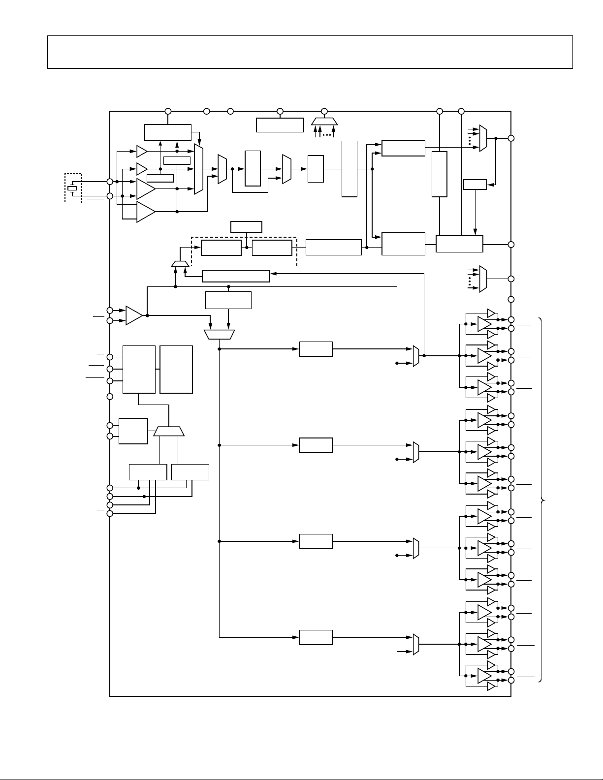
FUNCTIONAL BLOCK DIAGRAM
Clock Generator
AD9520-5
CP
Supports external 3.3 V/5 V VCO/VCXO to 2.4 GHz
1 differential or 2 single-ended reference inputs
Accepts CMOS, LVDS, or LVPECL references to 250 MHz
Accepts 16.67 MHz to 33.3 MHz crystal for reference input
Optional reference clock doubler
Reference monitoring capability
Auto and manual reference switchover/holdover modes,
with selectable revertive/nonrevertive switching
Glitch-free switchover between references
Automatic recovery from holdover
Digital or analog lock detect, selectable
Optional zero delay operation
Twelve 1.6 GHz LVPECL outputs divided into 4 groups
Each group of 3 has a 1-to-32 divider with phase delay
Additive output jitter as low as 225 fs rms
Channel-to-channel skew grouped outputs <16 ps
Each LVPECL output can be configured as 2 CMOS outputs
(for f
≤ 250 MHz)
OUT
Automatic synchronization of all outputs on power-up
Manual synchronization of outputs as needed
SPI- and I²C-compatible serial control port
64-lead LFCSP
Nonvolatile EEPROM stores configuration settings
APPLICATIONS
Low jitter, low phase noise clock distribution
Clock generation and translation for SONET, 10Ge, 10G FC,
and other 10 Gbps protocols
Forward error correction (G.710)
Clocking high speed ADCs, DACs, DDSs, DDCs, DUCs, MxFEs
High performance wireless transceivers
ATE and high performance instrumentation
Broadband infrastructures
GENERAL DESCRIPTION
The AD9520-51 provides a multioutput clock distribution
function with subpicosecond jitter performance, along with an
on-chip PLL that can be used with an external VCO.
The AD9520 serial interface supports both SPI and IC® ports.
An in-package EEPROM can be programmed through the serial
REF1
REFIN
REFIN
CLK
CLK
REF2
AND MUXES
SPI/I2C CONTROL
PORT AND
DIGITAL LOGIC
SWITCHOVER
AND MONITOR
DIVIDER
DIV/Φ
DIV/Φ
DIV/Φ
DIV/Φ
PLL
EEPROM
Figure 1.
The AD9520 features 12 LVPECL outputs in four groups. Any
of the 1.6 GHz LVPECL outputs can be reconfigured as two
250 MHz CMOS outputs.
Each group of outputs has a divider that allows both the divide
ratio (from 1 to 32) and the phase (coarse delay) to be set.
The AD9520 is available in a 64-lead LFCSP and can be operated
from a single 3.3 V supply. The external VCO can have an
operating voltage up to 5.5 V. A separate output driver power
supply can be from 2.375 V to 3.465 V.
The AD9520 is specified for operation over the standard industrial
range of −40°C to +85°C.
STATUS
MONITOR
DELAY
LVPECL/
CMOS
AD9520-5
ZERO
OUT0
OUT1
OUT2
OUT3
OUT4
OUT5
OUT6
OUT7
OUT8
OUT9
OUT10
OUT11
07239-001
interface and store user-defined register settings for power-up
and chip reset.
1
The AD9520 is used throughout this data sheet to refer to all the members of the AD9520 family. However, when AD9520-5 is used, it refers to that specific member of
the AD9520 family.
Rev. 0
Information furnished by Analog Devices is believed to be accurate and reliable. However, no
responsibility is assumed by Analog Devices for its use, nor for any infringements of patents or other
rights of third parties that may result from its use. Specifications subject to change without notice. No
license is granted by implication or otherwise under any patent or patent rights of Analog Devices.
Trademarks and registered trademarks are the property of their respective owners.
One Technology Way, P.O. Box 9106, Norwood, MA 02062-9106, U.S.A.
Tel: 781.329.4700 www.analog.com
Fax: 781.461.3113 ©2008 Analog Devices, Inc. All rights reserved.

AD9520-5
http://www.BDTIC.com/ADI
TABLE OF CONTENTS
Features .............................................................................................. 1
Applications ....................................................................................... 1
General Description ......................................................................... 1
Functional Block Diagram .............................................................. 1
Revision History ............................................................................... 3
Specifications ..................................................................................... 4
Power Supply Requirements ....................................................... 4
PLL Characteristics ...................................................................... 4
Clock Inputs .................................................................................. 7
Clock Outputs ............................................................................... 7
Timing Characteristics ................................................................ 8
Timing Diagrams ..................................................................... 9
Clock Output Additive Phase Noise
(Distribution Only; VCO Divider Not Used) ......................... 10
Clock Output Absolute Time Jitter
(Clock Generation Using External VCXO) ............................ 11
Clock Output Additive Time Jitter
(VCO Divider Not Used) .......................................................... 11
Clock Output Additive Time Jitter (VCO Divider Used) ..... 12
Serial Control Port—SPI Mode ................................................ 12
Serial Control Port—IC Mode ................................................ 13
SYNC
PD
,
Serial Port Setup Pins: SP1, SP0 ............................................... 14
LD, STATUS, and REFMON Pins ............................................ 14
Power Dissipation ....................................................................... 15
Absolute Maximum Ratings .......................................................... 16
Thermal Resistance .................................................................... 16
ESD Caution ................................................................................ 16
Pin Configuration and Function Descriptions ........................... 17
Typical Performance Characteristics ........................................... 20
Terminology .................................................................................... 24
Detailed Block Diagram ................................................................ 25
Theory of Operation ...................................................................... 26
Operational Configurations ...................................................... 26
Mode 1: Clock Distribution or
External VCO < 1600 MHz .................................................. 26
Mode 2: High Frequency Clock Distribution—
CLK or External VCO > 1600 MHz .................................... 28
, and
RESET
Pins ..................................................... 14
Rev. 0 | Page 2 of 80
Phase-Locked Loop (PLL) .................................................... 30
Configuration of the PLL ...................................................... 30
Phase Frequency Detector (PFD) ........................................ 30
Charge Pump (CP) ................................................................. 30
PLL External Loop Filter ....................................................... 31
PLL Reference Inputs ............................................................. 31
Reference Switchover ............................................................. 31
Reference Divider R ............................................................... 32
VCO/VCXO Feedback Divider N: P, A, B, R ..................... 32
Digital Lock Detect (DLD) ................................................... 33
Analog Lock Detect (ALD) ................................................... 34
Current Source Digital Lock Detect (CSDLD) .................. 34
External VCXO/VCO Clock Input (CLK/
Holdover .................................................................................. 34
External/Manual Holdover Mode ........................................ 35
Automatic/Internal Holdover Mode .................................... 35
Frequency Status Monitors ................................................... 37
Zero Delay Operation ................................................................ 38
Clock Distribution ..................................................................... 39
Operation Modes ................................................................... 39
CLK Direct-to-LVPECL Outputs ......................................... 39
Clock Frequency Division ..................................................... 40
VCO Divider ........................................................................... 40
Channel Dividers ................................................................... 40
Synchronizing the Outputs—
LVPECL Output Drivers ....................................................... 43
CMOS Output Drivers .......................................................... 44
Reset Modes ................................................................................ 44
Power-On Reset ...................................................................... 44
Hardware Reset via the
Soft Reset via the Serial Port ................................................. 44
Soft Reset to Settings in EEPROM when
EEPROM Pin = 0 via the Serial Port ..................................... 44
Power-Down Modes .................................................................. 44
Chip Power-Down via PD .................................................... 44
PLL Power-Down ................................................................... 45
Distribution Power-Down .................................................... 45
Individual Clock Output Power-Down ............................... 45
Individual Clock Channel Power-Down ............................. 45
SYNC
RESET
Pin ..................................... 44
CLK
) ................ 34
Function ................... 42

AD9520-5
http://www.BDTIC.com/ADI
Serial Control Port .......................................................................... 46
SPI/IC Port Selection ................................................................ 46
IC Serial Port Operation ........................................................... 46
2
I
C Bus Characteristics ........................................................... 46
Data Transfer Process ............................................................. 47
Data Transfer Format ............................................................. 48
IC Serial Port Timing ............................................................ 48
SPI Serial Port Operation ........................................................... 49
Pin Descriptions ...................................................................... 49
SPI Mode Operation ............................................................... 49
Communication Cycle—Instruction Plus Data .................. 49
Write ......................................................................................... 49
Read .......................................................................................... 49
SPI Instruction Word (16 Bits) .................................................. 50
SPI MSB/LSB First Transfers ..................................................... 50
EEPROM Operations ...................................................................... 53
Writing to the EEPROM ............................................................ 53
Reading from the EEPROM ...................................................... 53
Programming the EEPROM Buffer Segment.......................... 53
Register Section Definition Group ....................................... 54
IO_UPDATE (Operational Code 0x80) .............................. 54
End-of-Data (Operational Code 0xFF) ............................... 54
Pseudo-End-of-Data (Operational Code 0xFE) ................. 54
Thermal Performance ..................................................................... 55
Register Map .................................................................................... 56
Register Map Descriptions ............................................................. 61
Applications Information ............................................................... 75
Frequency Planning Using the AD9520 .................................. 75
Using the AD9520 Outputs for ADC Clock Applications .... 75
LVPECL Clock Distribution ...................................................... 75
CMOS Clock Distribution ......................................................... 76
Outline Dimensions ........................................................................ 77
Ordering Guide ........................................................................... 77
REVISION HISTORY
10/08—Revision 0: Initial Version
Rev. 0 | Page 3 of 80
AD9520-5
http://www.BDTIC.com/ADI
SPECIFICATIONS
Typical (typ) is given for VS = VS_DRV = 3.3 V ± 5%; VS ≤ VCP ≤ 5.25 V; TA = 25°C; RSET = 4.12 kΩ; CPRSET = 5.1 kΩ, unless otherwise
noted. Minimum (min) and maximum (max) values are given over full VS and T
POWER SUPPLY REQUIREMENTS
Table 1.
Parameter Min Typ Max Unit Test Conditions/Comments
VS 3.135 3.3 3.465 V 3.3 V ± 5%
VS_DRV 2.375 VS V This is nominally 2.5 V to 3.3 V ± 5%
VCP VS 5.25 V This is nominally 3.3 V to 5.0 V ± 5%
RSET Pin Resistor 4.12 kΩ Sets internal biasing currents; connect to ground
CPRSET Pin Resistor 5.1 kΩ
Sets internal CP current range, nominally 4.8 mA (CP_lsb = 600 μA);
actual current can be calculated by CP_lsb = 3.06/CPRSET; connect to ground
PLL CHARACTERISTICS
Table 2.
Parameter Min Typ Max Unit Test Conditions/Comments
REFERENCE INPUTS
Differential Mode (REFIN, REFIN)
Input Frequency 0 250 MHz
Input Sensitivity 280 mV p-p
Self-Bias Voltage, REFIN 1.34 1.60 1.75 V Self-bias voltage of REFIN
Self-Bias Voltage, REFIN
Input Resistance, REFIN 4.0 4.8 5.9 kΩ Self-biased
Input Resistance, REFIN
Dual Single-Ended Mode (REF1, REF2) Two single-ended CMOS-compatible inputs
Input Frequency (AC-Coupled)
with DC Offset Off)
Input Frequency (AC-Coupled
with DC Offset On)
Input Frequency (DC-Coupled) 0 250 MHz Slew rate > 50 V/μs; CMOS levels
Input Sensitivity (AC-Coupled
with DC Offset Off)
Input Sensitivity (AC-Coupled
with DC Offset On)
Input Logic High, DC Offset Off 2.0 V
Input Logic Low, DC Offset Off 0.8 V
Input Current −100 +100 μA
Input Capacitance 2 pF
Crystal Oscillator
Crystal Resonator Frequency Range 16.67 33.33 MHz
Maximum Crystal Motional Resistance 30 Ω
PHASE/FREQUENCY DETECTOR (PFD)
PFD Input Frequency 100 MHz Antibacklash pulse width = 1.3 ns, 2.9 ns
45 MHz Antibacklash pulse width = 6.0 ns
Reference Input Clock Doubler Frequency 0.004 50 MHz Antibacklash pulse width = 1.3 ns, 2.9 ns
Antibacklash Pulse Width 1.3 ns 0x017[1:0] = 01b
2.9 ns 0x017[1:0] = 00b; 0x017[1:0] = 11b
6.0 ns 0x017[1:0] = 10b
1.30 1.50 1.60 V
4.4 5.3 6.4 kΩ Self-biased
10 250 MHz Slew rate must be > 50 V/μs
250 MHz
0.55 3.28 V p-p VIH should not exceed VS
1.5 2.78 V p-p VIH should not exceed VS
(−40°C to +85°C) variation.
A
Differential mode (can accommodate single-ended
input by ac grounding undriven input)
Frequencies below about 1 MHz should be dc-coupled;
be careful to match VCM (self-bias voltage)
1
1
Self-bias voltage of REFIN
1
1
Slew rate must be > 50 V/μs, and input amplitude
sensitivity specification must be met; see input sensitivity
Each pin, REFIN (REF1)/REFIN
(REF2)
Rev. 0 | Page 4 of 80

AD9520-5
http://www.BDTIC.com/ADI
Parameter Min Typ Max Unit Test Conditions/Comments
CHARGE PUMP (CP)
ICP Sink/Source Programmable
High Value 4.8 mA
Low Value 0.60 mA
Absolute Accuracy 2.5 % Charge pump voltage set to VCP/2
CPRSET Range 2.7 10 kΩ
ICP High Impedance Mode Leakage 1 nA
Sink-and-Source Current Matching 1 %
ICP vs. VCP 1.5 % 0.5 V < VCP < VCP − 0.5 V
ICP vs. Temperature 2 % VCP = VCP/2 V
PRESCALER (PART OF N DIVIDER)
Prescaler Input Frequency
P = 1 FD 300 MHz
P = 2 FD 600 MHz
P = 3 FD 900 MHz
P = 2 DM (2/3) 600 MHz
P = 4 DM (4/5) 1000 MHz
P = 8 DM (8/9) 2400 MHz
P = 16 DM (16/17) 3000 MHz
P = 32 DM (32/33) 3000 MHz
Prescaler Output Frequency 300 MHz
PLL N DIVIDER DELAY Register 0x019[2:0]; see Table 48
000 Off
001 410 ps
010 530 ps
011 650 ps
100 770 ps
101 890 ps
110 1010 ps
111 1130 ps
PLL R DIVIDER DELAY Register 0x019[5:3]; see Table 48
000 Off
001 370 ps
010 490 ps
011 610 ps
100 730 ps
101 850 ps
110 970 ps
111 1090 ps
PHASE OFFSET IN ZERO DELAY
Phase Offset (REF-to-LVPECL Clock Output
Pins) in Internal Zero Delay Mode
Phase Offset (REF-to-LVPECL Clock Output
Pins) in Internal Zero Delay Mode
560 1060 1310 ps When N delay and R delay are bypassed
−320 +50 +240 ps When N delay = Setting 110 and R delay is bypassed
With CPRSET = 5.1 kΩ; higher I
changing CPRSET
With CPRSET = 5.1 kΩ; lower I
changing CPRSET
0.5 V < V
pump) pin; VCP is the voltage on the VCP power supply pin
A, B counter input frequency (prescaler input
frequency divided by P)
REF refers to REFIN (REF1)/REFIN
< VCP − 0.5 V; VCP is the voltage on the CP (charge
CP
is possible by
CP
is possible by
CP
(REF2)
Rev. 0 | Page 5 of 80
AD9520-5
http://www.BDTIC.com/ADI
Parameter Min Typ Max Unit Test Conditions/Comments
NOISE CHARACTERISTICS
In-Band Phase Noise of the Charge Pump/
Phase Frequency Detector (In-Band
Means Within the LBW of the PLL)
@ 500 kHz PFD Frequency −165 dBc/Hz
@ 1 MHz PFD Frequency −162 dBc/Hz
@ 10 MHz PFD Frequency −152 dBc/Hz
@ 50 MHz PFD Frequency −144 dBc/Hz
PLL Figure of Merit (FOM) −222 dBc/Hz
PLL DIGITAL LOCK DETECT WINDOW
2
Lock Threshold (Coincidence of Edges)
Low Range (ABP 1.3 ns, 2.9 ns) 3.5 ns 0x017[1:0] = 00b, 01b,11b; 0x018[4] = 1b
High Range (ABP 1.3 ns, 2.9 ns) 7.5 ns 0x017[1:0] = 00b, 01b, 11b; 0x018[4] = 0b
High Range (ABP 6.0 ns) 3.5 ns 0x017[1:0] = 10b; 0x018[4] = 0b
Unlock Threshold (Hysteresis)
2
Low Range (ABP 1.3 ns, 2.9 ns) 7 ns 0x017[1:0] = 00b, 01b, 11b; 0x018[4] = 1b
High Range (ABP 1.3 ns, 2.9 ns) 15 ns 0x017[1:0] = 00b, 01b, 11b; 0x018[4] = 0b
High Range (ABP 6.0 ns) 11 ns 0x017[1:0] = 10b; 0x018[4] = 0b
1
The REFIN and
2
For reliable operation of the digital lock detect, the period of the PFD frequency must be greater than the unlock-after-lock time.
REFIN
self-bias points are offset slightly to avoid chatter on an open input condition.
The PLL in-band phase noise floor is estimated by
measuring the in-band phase noise at the output of
the VCO and subtracting 20 log(N) (where N is the value
of the N divider)
Reference slew rate > 0.5 V/ns; FOM + 10 log(f
PFD
) is an
approximation of the PFD/CP in-band phase noise (in
the flat region) inside the PLL loop bandwidth; when
running closed-loop, the phase noise, as observed at
the VCO output, is increased by 20 log(N); PLL figure of
merit decreases with decreasing slew rate; see Figure 11
Signal available at the LD, STATUS, and REFMON pins
when selected by appropriate register settings; lock
detect window settings can be varied by changing the
CPRSET resistor
Selected by 0x017[1:0] and 0x018[4] (this is the threshold
to go from unlock to lock)
Selected by 0x017[1:0] and 0x018[4] (this is the threshold
to go from lock to unlock)
Rev. 0 | Page 6 of 80
AD9520-5
http://www.BDTIC.com/ADI
CLOCK INPUTS
Table 3.
Parameter Min Typ Max Unit Test Conditions/Comments
CLOCK INPUTS (CLK, CLK)
Input Frequency 0
0
Input Sensitivity, Differential 150 mV p-p
Input Level, Differential 2 V p-p
Input Common-Mode Voltage, VCM 1.3 1.57 1.8 V Self-biased; enables ac coupling
Input Common-Mode Range, V
1.3 1.8 V With 200 mV p-p signal applied; dc-coupled
CMR
Input Sensitivity, Single-Ended 150 mV p-p
Input Resistance 3.9 4.7 5.7 kΩ Self-biased
Input Capacitance 2 pF
1
Below about 1 MHz, the input should be dc-coupled. Care should be taken to match VCM.
CLOCK OUTPUTS
Table 4.
Parameter Min Typ Max Unit Test Conditions/Comments
LVPECL CLOCK OUTPUTS Termination = 50 Ω to VS_DRV − 2 V
OUT0, OUT1, OUT2, OUT3,
OUT4, OUT5, OUT6, OUT7,
OUT8, OUT9, OUT10, OUT11
Output Frequency, Maximum 2400 MHz
Output High Voltage, VOH VS_DRV − 1.07 VS_DRV − 0.96 VS_DRV − 0.84 V
Output Low Voltage, VOL VS_DRV − 1.95 VS_DRV − 1.79 VS_DRV − 1.64 V
Output Differential Voltage, VOD 660 820 950 mV
CMOS CLOCK OUTPUTS
OUT0A, OUT0B, OUT1A, OUT1B,
OUT2A, OUT2B, OUT3A, OUT3B,
OUT4A, OUT4B, OUT5A, OUT5B,
OUT6A, OUT6B, OUT7A, OUT7B,
OUT8A, OUT8B, OUT9A, OUT9B,
OUT10A, OUT10B, OUT11A,
OUT11B
Output Frequency 250 MHz See Figure 18
Output Voltage High, VOH VS − 0.1 V @ 1 mA load, VS_DRV = 3.3 V/2.5 V
Output Voltage Low, VOL 0.1 V @ 1 mA load, VS_DRV = 3.3 V/2.5 V
Output Voltage High, VOH 2.7 V @ 10 mA load, VS_DRV = 3.3 V
Output Voltage Low, VOL 0.5 V @ 10 mA load, VS_DRV = 3.3 V
Output Voltage High, VOH 1.8 V @ 10 mA load, VS_DRV = 2.5 V
Output Voltage Low, VOL 0.6 V @ 10 mA load, VS_DRV = 2.5 V
Differential input
1
2.4 GHz High frequency distribution (VCO divider)
1
1.6 GHz
Distribution only (VCO divider bypassed); this is the
frequency range supported by the channel divider
Measured at 2.4 GHz; jitter performance is improved with
slew rates > 1 V/ns
Larger voltage swings can turn on the protection diodes
and can degrade jitter performance
CLK ac-coupled; CLK
ac-bypassed to RF ground
Differential (OUT, OUT)
Using direct to output; see Figure 17
(higher frequencies are possible, but
amplitude will not meet the V
OD
specification); the maximum output
frequency is limited by the maximum
frequency at the CLK inputs
Single-ended; termination = 10 pF
Rev. 0 | Page 7 of 80

AD9520-5
http://www.BDTIC.com/ADI
TIMING CHARACTERISTICS
Table 5.
Parameter Min Typ Max Unit Test Conditions/Comments
LVPECL OUTPUT RISE/FALL TIMES Termination = 50 Ω to VS_DRV − 2 V
Output Rise Time, tRP 130 170 ps
Output Fall Time, tFP 130 170 ps
PROPAGATION DELAY, t
, CLK-TO-LVPECL OUTPUT
PECL
For All Divide Values 850 1050 1280 ps High frequency clock distribution configuration
800 970 1180 ps Clock distribution configuration
Variation with Temperature 1.0 ps/°C
OUTPUT SKEW, LVPECL OUTPUTS
1
Termination = 50 Ω to VS_DRV − 2 V
LVPECL Outputs That Share the Same Divider 5 16 ps VS_DRV = 3.3 V
5 20 ps VS_DRV = 2.5 V
LVPECL Outputs on Different Dividers 5 45 ps VS_DRV = 3.3 V
5 60 ps VS_DRV = 2.5 V
All LVPECL Outputs Across Multiple Parts 190 ps VS_DRV = 3.3 V and 2.5 V
CMOS OUTPUT RISE/FALL TIMES Termination = open
Output Rise Time, tRC 750 960 ps 20% to 80%; C
Output Fall Time, tFC 715 890 ps 80% to 20%; C
Output Rise Time, tRC 965 1280 ps 20% to 80%; C
Output Fall Time, tFC 890 1100 ps 80% to 20%; C
PROPAGATION DELAY, t
, CLK-TO-CMOS OUTPUT Clock distribution configuration
CMOS
For All Divide Values 2.1 2.75 3.55 ns VS_DRV = 3.3 V
3.35 ns VS_DRV = 2.5 V
Variation with Temperature 2 ps/°C VS_DRV = 3.3 V and 2.5 V
OUTPUT SKEW, CMOS OUTPUTS
1
CMOS Outputs That Share the Same Divider 7 85 ps VS_DRV = 3.3 V
10 105 ps VS_DRV = 2.5 V
All CMOS Outputs on Different Dividers 10 240 ps VS_DRV = 3.3 V
10 285 ps VS_DRV = 2.5 V
All CMOS Outputs Across Multiple Parts 600 ps VS_DRV = 3.3 V
620 ps VS_DRV = 2.5 V
OUTPUT SKEW, LVPECL-TO-CMOS OUTPUT
1
All settings identical; different logic type
Outputs That Share the Same Divider 1.18 1.76 2.48 ns LVPECL to CMOS on same part
Outputs That Are on Different Dividers 1.20 1.78 2.50 ns LVPECL to CMOS on same part
1
The output skew is the difference between any two similar delay paths while operating at the same voltage and temperature.
20% to 80%, measured differentially (rise/fall
times are independent of VS and are valid for
VS_DRV = 3.3 V and 2.5 V)
80% to 20%, measured differentially (rise/fall
times are independent of VS and are valid for
VS_DRV = 3.3 V and 2.5 V)
= 10 pF; VS_DRV = 3.3 V
LOAD
= 10 pF; VS_DRV = 3.3 V
LOAD
= 10 pF; VS_DRV = 2.5 V
LOAD
= 10 pF; VS_DRV = 2.5 V
LOAD
Rev. 0 | Page 8 of 80
AD9520-5
K
http://www.BDTIC.com/ADI
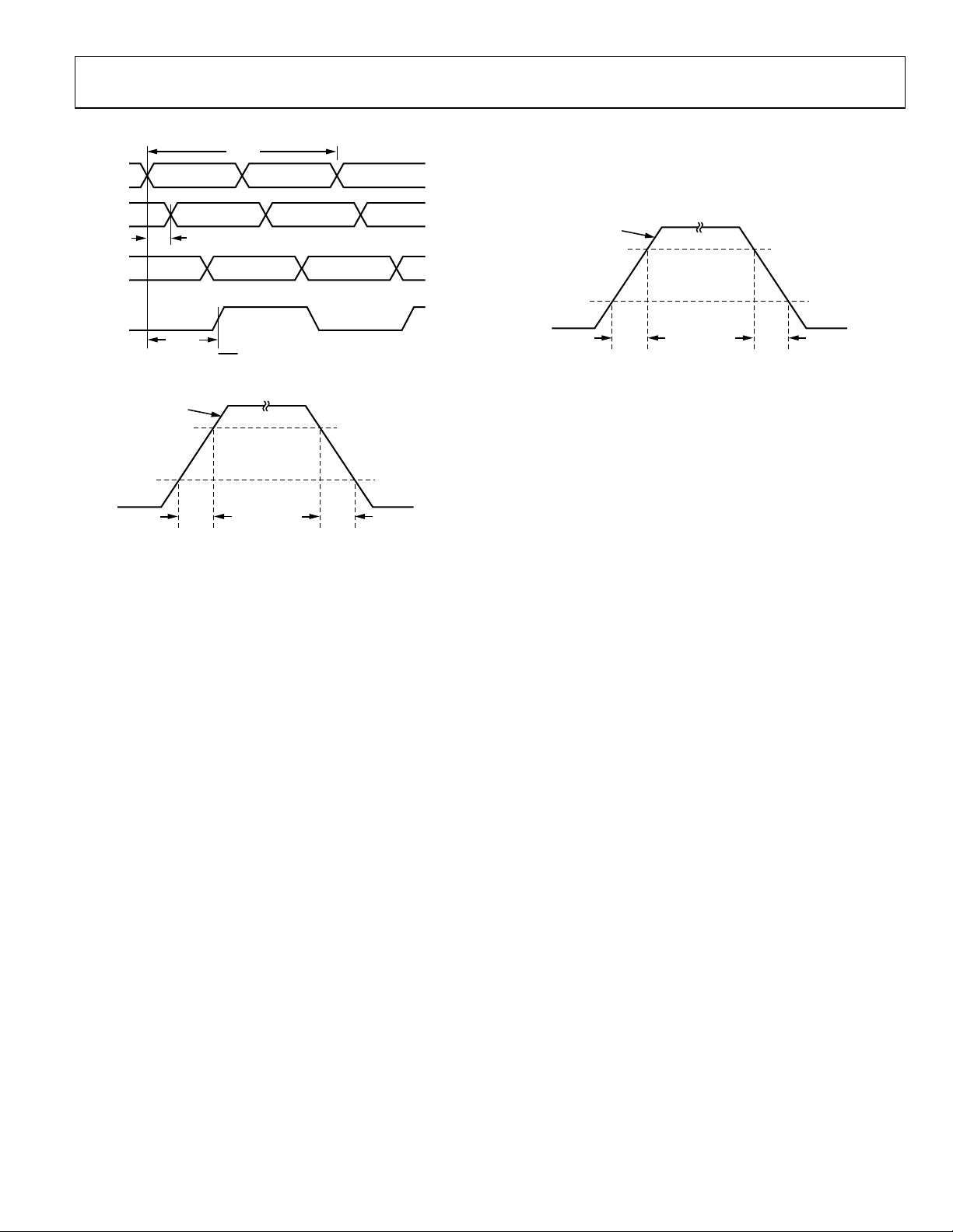
Timing Diagrams
t
CLK
CL
t
t
CMOS
Figure 2. CLK/
DIFFERENTIAL
80%
20%
t
PECL
CLK
to Clock Output Timing, DIV = 1
LVPECL
RP
07239-060
t
FP
07239-061
SINGL E-ENDE D
80%
CMOS
10pF LOAD
20%
t
RC
t
FC
Figure 4. CMOS Timing, Single-Ended, 10 pF Load
07239-063
Figure 3. LVPECL Timing, Differential
Rev. 0 | Page 9 of 80

AD9520-5
http://www.BDTIC.com/ADI
CLOCK OUTPUT ADDITIVE PHASE NOISE (DISTRIBUTION ONLY; VCO DIVIDER NOT USED)
Table 6.
Parameter Min Typ Max Unit Test Conditions/Comments
CLK-TO-LVPECL ADDITIVE PHASE NOISE Distribution section only; does not include the PLL
CLK = 1 GHz, Output = 1 GHz Input slew rate > 1 V/ns
Divider = 1
@ 10 Hz Offset −107 dBc/Hz
@ 100 Hz Offset −117 dBc/Hz
@ 1 kHz Offset −127 dBc/Hz
@ 10 kHz Offset −135 dBc/Hz
@ 100 kHz Offset −142 dBc/Hz
@ 1 MHz Offset −145 dBc/Hz
@ 10 MHz Offset −147 dBc/Hz
@ 100 MHz Offset −150 dBc/Hz
CLK = 1 GHz, Output = 200 MHz Input slew rate > 1 V/ns
Divider = 5
@ 10 Hz Offset −122 dBc/Hz
@ 100 Hz Offset −132 dBc/Hz
@ 1 kHz Offset −143 dBc/Hz
@ 10 kHz Offset −150 dBc/Hz
@ 100 kHz Offset −156 dBc/Hz
@ 1 MHz Offset −157 dBc/Hz
>10 MHz Offset −157 dBc/Hz
CLK-TO-CMOS ADDITIVE PHASE NOISE Distribution section only; does not include the PLL
CLK = 1 GHz, Output = 250 MHz Input slew rate > 1 V/ns
Divider = 4
@ 10 Hz Offset −107 dBc/Hz
@ 100 Hz Offset −119 dBc/Hz
@ 1 kHz Offset −125 dBc/Hz
@ 10 kHz Offset −134 dBc/Hz
@ 100 kHz Offset −144 dBc/Hz
@ 1 MHz Offset −148 dBc/Hz
>10 MHz Offset −154 dBc/Hz
CLK = 1 GHz, Output = 50 MHz Input slew rate > 1 V/ns
Divider = 20
@ 10 Hz Offset −126 dBc/Hz
@ 100 Hz Offset −133 dBc/Hz
@ 1 kHz Offset −140 dBc/Hz
@ 10 kHz Offset −148 dBc/Hz
@ 100 kHz Offset −157 dBc/Hz
@ 1 MHz Offset −160 dBc/Hz
>10 MHz Offset −163 dBc/Hz
Rev. 0 | Page 10 of 80
AD9520-5
http://www.BDTIC.com/ADI
CLOCK OUTPUT ABSOLUTE TIME JITTER (CLOCK GENERATION USING EXTERNAL VCXO)
Table 7.
Parameter Min Typ Max Unit Test Conditions/Comments
LVPECL OUTPUT ABSOLUTE TIME JITTER
LVPECL = 245.76 MHz; PLL LBW = 125 Hz 54 fs rms Integration BW = 200 kHz to 5 MHz
77 fs rms Integration BW = 200 kHz to 10 MHz
109 fs rms Integration BW = 12 kHz to 20 MHz
LVPECL = 122.88 MHz; PLL LBW = 125 Hz 79 fs rms Integration BW = 200 kHz to 5 MHz
114 fs rms Integration BW = 200 kHz to 10 MHz
163 fs rms Integration BW = 12 kHz to 20 MHz
LVPECL = 61.44 MHz; PLL LBW = 125 Hz 124 fs rms Integration BW = 200 kHz to 5 MHz
176 fs rms Integration BW = 200 kHz to 10 MHz
259 fs rms Integration BW = 12 kHz to 20 MHz
CLOCK OUTPUT ADDITIVE TIME JITTER (VCO DIVIDER NOT USED)
Table 8.
Parameter Min Typ Max Unit Test Conditions/Comments
LVPECL OUTPUT ADDITIVE TIME JITTER
CLK = 622.08 MHz 46 fs rms Integration bandwidth = 12 kHz to 20 MHz
Any LVPECL Output = 622.08 MHz
Divide Ratio = 1
CLK = 622.08 MHz 64 fs rms Integration bandwidth = 12 kHz to 20 MHz
Any LVPECL Output = 155.52 MHz
Divide Ratio = 4
CLK = 1000 MHz 223 fs rms Calculated from SNR of ADC method
Any LVPECL Output = 100 MHz Broadband jitter
Divide Ratio = 10
CLK = 500 MHz 209 fs rms Calculated from SNR of ADC method
Any LVPECL Output = 100 MHz Broadband jitter
Divide Ratio = 5
CMOS OUTPUT ADDITIVE TIME JITTER Distribution section only; does not include the PLL
CLK = 200 MHz 325 fs rms Calculated from SNR of ADC method
Any CMOS Output Pair = 100 MHz Broadband jitter
Divide Ratio = 2
Application example based on a typical setup using an
external 245.76 MHz VCXO (Toyocom TCO-2112);
reference = 15.36 MHz; R DIV = 1
Distribution section only; does not include the PLL;
measured at rising edge of clock signal
Rev. 0 | Page 11 of 80
AD9520-5
http://www.BDTIC.com/ADI
CLOCK OUTPUT ADDITIVE TIME JITTER (VCO DIVIDER USED)
Table 9.
Parameter Min Typ Max Unit Test Conditions/Comments
LVPECL OUTPUT ADDITIVE TIME JITTER
CLK = 1.0 GHz; VCO DIV = 5; LVPECL = 100 MHz;
Channel Divider = 2; Duty-Cycle Correction = Off
CLK = 500 MHz; VCO DIV = 5; LVPECL = 100 MHz;
Bypass Channel Divider; Duty-Cycle Correction = On
CMOS OUTPUT ADDITIVE TIME JITTER
CLK = 200 MHz; VCO DIV = 2; CMOS = 100 MHz;
Bypass Channel Divider; Duty-Cycle Correction = Off
CLK = 1600 MHz; VCO DIV = 2; CMOS = 100 MHz;
Channel Divider = 8; Duty-Cycle Correction = Off
230 fs rms
215 fs rms
326 fs rms
362 fs rms
SERIAL CONTROL PORT—SPI MODE
Table 10.
Parameter Min Typ Max Unit Test Conditions/Comments
CS (INPUT)
Input Logic 1 Voltage 2.0 V
Input Logic 0 Voltage 0.8 V
Input Logic 1 Current 3 μA
Input Logic 0 Current −110 μA
Input Capacitance 2 pF
SCLK (INPUT) IN SPI MODE
Input Logic 1 Voltage 2.0 V
Input Logic 0 Voltage 0.8 V
Input Logic 1 Current 110 μA
Input Logic 0 Current 1 μA
Input Capacitance 2 pF
SDIO (WHEN AN INPUT IN BIDIRECTIONAL MODE)
Input Logic 1 Voltage 2.0 V
Input Logic 0 Voltage 0.8 V
Input Logic 1 Current 1 μA
Input Logic 0 Current 1 μA
Input Capacitance 2 pF
SDIO, SDO (OUTPUTS)
Output Logic 1 Voltage 2.7 V
Output Logic 0 Voltage 0.4 V
TIMING
Clock Rate (SCLK, 1/t
Pulse Width High, t
Pulse Width Low, t
SDIO to SCLK Setup, tDS 4 ns
SCLK to SDIO Hold, tDH 0 ns
SCLK to Valid SDIO and SDO, tDV 11 ns
CS to SCLK Setup and Hold, tS, tC
CS Minimum Pulse Width High, t
) 25 MHz
SCLK
16 ns
HIGH
16 ns
LOW
PWH
2 ns
3 ns
CS has an internal 30 kΩ pull-up resistor
The minus sign indicates that current is flowing out of
the AD9520, which is due to the internal pull-up resistor
SCLK has an internal 30 kΩ pull-down resistor in SPI
mode, but not in I2C mode
Distribution section only; does not include PLL
and VCO; uses rising edge of clock signal
Calculated from SNR of ADC method
(broadband jitter)
Calculated from SNR of ADC method
(broadband jitter)
Distribution section only; does not include PLL;
uses rising edge of clock signal
Calculated from SNR of ADC method
(broadband jitter)
Calculated from SNR of ADC method
(broadband jitter)
Rev. 0 | Page 12 of 80

AD9520-5
http://www.BDTIC.com/ADI
SERIAL CONTROL PORT—I²C MODE
Table 11.
Parameter Min Typ Max Unit Test Conditions/Comments
SDA, SCL (WHEN INPUTTING DATA)
Input Logic 1 Voltage 0.7 × VS V
Input Logic 0 Voltage 0.3 × VS V
Input Current with an Input Voltage Between 0.1 × VS
and 0.9 × VS
Hysteresis of Schmitt Trigger Inputs 0.015 × VS V
Pulse Width of Spikes That Must Be Suppressed by the
Input Filter, t
SPIKE
SDA (WHEN OUTPUTTING DATA)
Output Logic 0 Voltage at 3 mA Sink Current 0.4 V
Output Fall Time from VIH
MIN
to VIL
with a Bus
MAX
Capacitance from 10 pF to 400 pF
TIMING
Clock Rate (SCL, f
Bus Free Time Between a Stop and Start Condition, t
Setup Time for a Repeated Start Condition, t
) 400 kHz
I2C
IDLE
0.6 μs
SET; STR
Hold Time (Repeated) Start Condition (After This Period,
the First Clock Pulse Is Generated), t
Setup Time for Stop Condition, t
Low Period of the SCL Clock, t
High Period of the SCL Clock, t
SCL, SDA Rise Time, t
SCL, SDA Fall Time, t
Data Setup Time, t
Data Hold Time, t
RISE
FAL L
SET; DAT
HLD; DAT
LOW
HIGH
20 + 0.1 Cb 300 ns
20 + 0.1 Cb 300 ns
120 ns
140 880 ns
SET; STP
1.3 μs
0.6 μs
HLD; STR
0.6 μs
Capacitive Load for Each Bus Line, Cb 400 pF
1
According to the original I2C specification, an I2C master must also provide a minimum hold time of 300 ns for the SDA signal to bridge the undefined region of the SCL
falling edge.
−10 +10 μA
50 ns
20 + 0.1 C
250 ns Cb = capacitance of one bus line in pF
b
Note that all I
referred to VIH
VIL
MAX
1.3 μs
0.6 μs
This is a minor deviation from the
original I²C specification of 100 ns
minimum
This is a minor deviation from the
original I²C specification of 0 ns
minimum
2
C timing values
(0.3 × VS) and
MIN
levels (0.7 × VS)
1
Rev. 0 | Page 13 of 80
AD9520-5
http://www.BDTIC.com/ADI
PD, SYNC, AND RESET PINS
Table 12.
Parameter Min Typ Max Unit Test Conditions/Comments
INPUT CHARACTERISTICS Each of these pins has a 30 kΩ internal pull-up resistor
Logic 1 Voltage 2.0 V
Logic 0 Voltage 0.8 V
Logic 1 Current 1 μA
Logic 0 Current −110 μA
Capacitance 2 pF
RESET TIMING
Pulse Width Low 50 ns
RESET Inactive to Start of Register Programming
SYNC TIMING
Pulse Width Low 1.3 ns High speed clock is CLK input signal
100 ns
SERIAL PORT SETUP PINS: SP1, SP0
Table 13.
Parameter Min Typ Max Unit Test Conditions/Comments
SP1, SP0 These pins do not have internal pull-up/pull-down resistors
Logic Level 0 0.25 × VS V VS is the voltage on the VS pin
Logic Level ½ 0.4 × VS 0.65 × VS V
Logic Level 1 0.8 × VS V
User can float these pins to obtain Logic Level ½; if floating this pin, user
should connect a capacitor to ground
The minus sign indicates that current is flowing out of
the AD9520, which is due to the internal pull-up resistor
LD, STATUS, AND REFMON PINS
Table 14.
Parameter Min Typ Max Unit Test Conditions/Comments
OUTPUT CHARACTERISTICS
Output Voltage High, VOH 2.7 V
Output Voltage Low, VOL 0.4 V
MAXIMUM TOGGLE RATE 100 MHz
ANALOG LOCK DETECT
Capacitance 3 pF
REF1, REF2, AND CLK FREQUENCY STATUS MONITOR
Normal Range 1.02 MHz
Extended Range 8 kHz
LD PIN COMPARATOR
Trip Point 1.6 V
Hysteresis 260 mV
When selected as a digital output (CMOS); there are other
modes in which these pins are not CMOS digital outputs;
see Table 48, 0x017, 0x01A, and 0x01B
Applies when mux is set to any divider or counter output
or PFD up/down pulse; also applies in analog lock detect
mode; usually debug mode only; beware that spurs can
couple to output when any of these pins is toggling
On-chip capacitance; used to calculate RC time constant
for analog lock detect readback; use a pull-up resistor
Frequency above which the monitor indicates the
presence of the reference
Frequency above which the monitor indicates the
presence of the reference
Rev. 0 | Page 14 of 80
AD9520-5
http://www.BDTIC.com/ADI
POWER DISSIPATION
Table 15.
Parameter Min Typ Max Unit Test Conditions/Comments
POWER DISSIPATION, CHIP
Power-On Default 1.32 1.5 W No clock; no programming; default register values
Distribution Only Mode; VCO Divider On;
0.39 0.46 W
One LVPECL Output Enabled
Distribution Only Mode; VCO Divider Off;
0.36 0.42 W
One LVPECL Output Enabled
Maximum Power, Full Operation 1.4 1.7 W
PD Power-Down
PD Power-Down, Maximum Sleep
60 80 mW
24 33 mW
VCP Supply 4 4.8 mW PLL operating; typical closed-loop configuration
POWER DELTAS, INDIVIDUAL FUNCTIONS Power delta when a function is enabled/disabled
VCO Divider On/Off 32 40 mW VCO divider not used
REFIN (Differential) Off 25 30 mW
REF1, REF2 (Single-Ended) On/Off 15 20 mW
PLL Dividers and Phase Detector
51 63 mW PLL off to PLL on, normal operation; no reference enabled
On/Off
LVPECL Channel 121 144 mW
LVPECL Driver 51 73 mW Second LVPECL output turned on, same channel
CMOS Channel 145 180 mW
CMOS Driver On/Off 11 24 mW Additional CMOS outputs within the same channel turned on
Channel Divider Enabled 40 57 mW
Zero Delay Block On/Off 30 34 mW
Does not include power dissipated in external resistors; all
LVPECL outputs terminated with 50 Ω to V
− 2 V; all CMOS
CC
outputs have 10 pF capacitive loading; VS_DRV = 3.3 V
= 2.4 GHz; f
f
CLK
= 200 MHz; VCO divider = 2; one LVPECL
OUT
output and output divider enabled; zero delay off
= 2.4 GHz; f
f
CLK
= 200 MHz; VCO divider bypassed; one
OUT
LVPECL output and output divider enabled; zero delay off
PLL on; VCO divider = 2; all channel dividers on; 12 LVPECL
outputs @ 125 MHz; zero delay on
PD pin pulled low; does not include power dissipated in
termination resistors
PD pin pulled low; PLL power-down, 0x010[1:0] = 01b;
power-down SYNC, 0x230[2] = 1b; power-down distribution
reference, 0x230[1] = 1b
Delta between reference input off and differential reference
input mode
Delta between reference inputs off and one singled-ended
reference enabled; double this number if both REF1 and REF2
are powered up
No LVPECL output on to one LVPECL output on; channel divider
set to 1
No CMOS output on to one CMOS output on; channel divider
set to 1; f
= 62.5 MHz and 10 pF of capacitive loading
OUT
Delta between divider bypassed (divide-by-1) and divide-by-2 to
divide-by-32
Rev. 0 | Page 15 of 80
AD9520-5
http://www.BDTIC.com/ADI
ABSOLUTE MAXIMUM RATINGS
Table 16.
With
Parameter or Pin
Respect to Rating
VS GND −0.3 V to +3.6 V
VCP, CP GND −0.3 V to +5.8 V
VS_DRV GND −0.3 V to +3.6 V
REFIN, REFIN
GND
−0.3 V to VS + 0.3 V
RSET GND −0.3 V to VS + 0.3 V
CPRSET GND −0.3 V to VS + 0.3 V
CLK, CLK
CLK
SCLK/SCL, SDIO/SDA, SDO, CS
OUT0, OUT0, OUT1, OUT1,
OUT2, OUT2
OUT4, OUT4
, OUT3, OUT3,
, OUT5, OUT5,
GND
CLK
GND
GND
−0.3 V to VS + 0.3 V
−1.2 V to +1.2 V
−0.3 V to VS + 0.3 V
−0.3 V to VS + 0.3 V
OUT6, OUT6, OUT7, OUT7,
OUT8, OUT8, OUT9, OUT9,
OUT10, OUT10
OUT11
SYNC, RESET, PD
, OUT11,
GND −0.3 V to VS + 0.3 V
REFMON, STATUS, LD GND −0.3 V to VS + 0.3 V
SP0, SP1, EEPROM GND −0.3 V to VS + 0.3 V
Junction Temperature
1
150°C
Storage Temperature Range −65°C to +150°C
Lead Temperature (10 sec) 300°C
1
See Table 17 for θJA.
Stresses above those listed under Absolute Maximum Ratings
may cause permanent damage to the device. This is a stress
rating only; functional operation of the device at these or any
other conditions above those indicated in the operational
section of this specification is not implied. Exposure to absolute
maximum rating conditions for extended periods may affect
device reliability.
THERMAL RESISTANCE
Thermal impedance measurements were taken on a JEDEC
JESD51-5 2S2P test board in still air in accordance with JEDEC
JESD51-2. See the Thermal Performance section for more
details.
Table 17.
Package Type θJA Unit
64-Lead LFCSP (CP-64-4) 22 °C/W
ESD CAUTION
Rev. 0 | Page 16 of 80
AD9520-5
http://www.BDTIC.com/ADI
PIN CONFIGURATION AND FUNCTION DESCRIPTIONS
REFIN (REF 1)
REFIN (REF 2)
CPRSETVSVS
GND
RSETVSOUT0 (OUT0A)
OUT0 (OUT0B)
VS_DRV
OUT1 (OUT1A)
OUT1 (OUT1B)
OUT2 (OUT2A)
OUT2 (OUT2B)
VS
49
48
OUT3 (OUT3A)
47
OUT3 (OUT3B)
46
VS_DRV
45
OUT4 (OUT4A)
44
OUT4 (OUT4B)
43
OUT5 (OUT5A)
42
OUT5 (OUT5B)
41
VS
40
VS
39
OUT8 (OUT8B)
38
OUT8 (OUT8A)
37
OUT7 (OUT7B)
36
OUT7 (OUT7A)
35
VS_DRV
34
OUT6 (OUT6B)
33
OUT6 (OUT6A)
VS
REFMON
LD
VCP
CP
STATUS
REF_SEL
SYNC
NC
NC
VS
VS
CLK
CLK
CS
SCLK/SCL
646362616059585756555453525150
1
PIN 1
INDICATO R
2
3
4
5
6
7
8
9
10
11
12
13
14
15
16
AD9520-5
TOP VIEW
(Not to Scale)
171819202122232425262728293031
PD
SP1
SP0
SDO
GND
RESET
T9 (OUT9A)
OU
VS_DRV
T9 (OUT9B)
OU
SDIO/SDA
NOTES
1. EXPOSED DIE PAD MUST BE CONNECTED TO GND.
EEPROM
OUT10A)
OUT10 (
OUT10B)
OUT10 (
OUT11A)
OUT11 (
OUT11B)
OUT11 (
32
VS
07239-003
Figure 5. Pin Configuration
Table 18. Pin Function Descriptions
Pin No.
1, 11, 12, 32,
Input/
Output
I Power VS 3.3 V Power Pins.
Pin
Type Mnemonic Description
40, 41,49,
57, 60, 61
2 O 3.3 V CMOS REFMON Reference Monitor (Output). This pin has multiple selectable outputs.
3 O 3.3 V CMOS LD
4 I Power VCP
Lock Detect (Output). This pin has multiple selectable outputs.
Power Supply for Charge Pump (CP); VS < VCP < 5.0 V. VCP must still be connected
to 3.3 V if the PLL is not used.
5 O Loop filter CP
Charge Pump (Output). This pin connects to an external loop filter. This pin can
be left unconnected if the PLL is not used.
6 O 3.3 V CMOS STATUS
7 I 3.3 V CMOS REF_SEL
Programmable Status Output.
Reference Select. It selects REF1 (low) or REF2 (high). This pin has an internal 30 kΩ
pull-down resistor.
8 I 3.3 V CMOS
SYNC
Manual Synchronization and Manual Holdover. This pin initiates a manual
synchronization and is used for manual holdover. Active low. This pin has an
internal 30 kΩ pull-up resistor.
9, 10 NC
13 I
Differential
CLK
No Connect. These pins can be left floating.
Along with CLK
, this pin is the differential input for the clock distribution section.
clock input
14 I
Differential
clock input
CLK
Along with CLK, this pin is the differential input for the clock distribution section. If a
single-ended input is connected to the CLK pin, connect a 0.1 μF bypass capacitor
from CLK to ground.
Rev. 0 | Page 17 of 80
AD9520-5
http://www.BDTIC.com/ADI
Input/
Pin No.
Output
15 I 3.3 V CMOS
16 I 3.3 V CMOS SCLK/SCL
17 I/O 3.3 V CMOS SDIO/SDA Serial Control Port Bidirectional Serial Data In/Out.
18 O 3.3 V CMOS SDO Serial Control Port Unidirectional Serial Data Out.
19, 59 I GND GND Ground Pins.
20 I
21 I
22 I 3.3 V CMOS EEPROM
23 I 3.3 V CMOS
24 I 3.3 V CMOS
25 O
26 O
27, 35,
I Power VS_DRV
46, 54
28 O
29 O
30 O
31 O
33 O
34 O
36 O
37 O
38 O
39 O
42 O
43 O
44 O
45 O
Pin
Type Mnemonic Description
Serial Control Port Chip Select; Active Low. This pin has an internal 30 kΩ pull-up
CS
resistor.
Serial Control Port Clock Signal. This pin has an internal 30 kΩ pull-down resistor
in SPI mode but is high impedance in I²C mode.
Three-level
logic
Three-level
logic
SP1
SP0
Select SPI or I²C as the serial interface port and select the I²C slave address in I²C
mode. Three-level logic. This pin is internally biased for the open logic level.
Select SPI or I²C as the serial interface port and select the I²C slave address in I²C
mode. Three-level logic. This pin is internally biased for the open logic level.
Setting this pin high selects the register values stored in the internal EEPROM to
be loaded at reset and/or power-up. Setting this pin low causes the AD9520 to
load the hard-coded default register values at power-up/reset. This pin has an
internal 30 kΩ pull-down resistor.
Chip Reset, Active Low. This pin has an internal 30 kΩ pull-up resistor.
Chip Power-Down, Active Low. This pin has an internal 30 kΩ pull-up resistor.
Clock Output. This pin can be configured as one side of a differential LVPECL
output or as a single-ended CMOS output.
output or as a single-ended CMOS output.
LVPECL or
CMOS
LVPECL or
CMOS
RESET
PD
OUT9 (OUT9A)
(OUT9B) Clock Output. This pin can be configured as one side of a differential LVPECL
OUT9
Output Driver Power Supply Pins. As a group, these pins can be set to either
2.5 V or 3.3 V. All four pins must be set to the same voltage.
LVPECL or
CMOS
LVPECL or
CMOS
LVPECL or
CMOS
LVPECL or
CMOS
LVPECL or
CMOS
LVPECL or
CMOS
LVPECL or
CMOS
LVPECL or
CMOS
LVPECL or
CMOS
LVPECL or
CMOS
LVPECL or
CMOS
LVPECL or
CMOS
LVPECL or
CMOS
LVPECL or
CMOS
OUT10 (OUT10A)
Clock Output. This pin can be configured as one side of a differential LVPECL
output or as a single-ended CMOS output.
(OUT10B) Clock Output. This pin can be configured as one side of a differential LVPECL
OUT10
output or as a single-ended CMOS output.
OUT11 (OUT11A)
Clock Output. This pin can be configured as one side of a differential LVPECL
output or as a single-ended CMOS output.
(OUT11B) Clock Output. This pin can be configured as one side of a differential LVPECL
OUT11
output or as a single-ended CMOS output.
OUT6 (OUT6A)
Clock Output. This pin can be configured as one side of a differential LVPECL
output or as a single-ended CMOS output.
(OUT6B) Clock Output. This pin can be configured as one side of a differential LVPECL
OUT6
output or as a single-ended CMOS output.
OUT7 (OUT7A)
Clock Output. This pin can be configured as one side of a differential LVPECL
output or as a single-ended CMOS output.
(OUT7B) Clock Output. This pin can be configured as one side of a differential LVPECL
OUT7
output or as a single-ended CMOS output.
OUT8 (OUT8A)
Clock Output. This pin can be configured as one side of a differential LVPECL
output or as a single-ended CMOS output.
(OUT8B) Clock Output. This pin can be configured as one side of a differential LVPECL
OUT8
output or as a single-ended CMOS output.
(OUT5B) Clock Output. This pin can be configured as one side of a differential LVPECL
OUT5
output or as a single-ended CMOS output.
OUT5 (OUT5A)
Clock Output. This pin can be configured as one side of a differential LVPECL
output or as a single-ended CMOS output.
(OUT4B) Clock Output. This pin can be configured as one side of a differential LVPECL
OUT4
output or as a single-ended CMOS output.
OUT4 (OUT4A)
Clock Output. This pin can be configured as one side of a differential LVPECL
output or as a single-ended CMOS output.
Rev. 0 | Page 18 of 80
AD9520-5
http://www.BDTIC.com/ADI
Input/
Pin No.
47 O
48 O
50 O
51 O
52 O
53 O
55 O
56 O
58 O
62 O
63 I
64 I
EPAD GND GND The exposed die pad must be connected to GND.
Output
Pin
Type Mnemonic Description
LVPECL or
CMOS
LVPECL or
CMOS
LVPECL or
CMOS
LVPECL or
CMOS
LVPECL or
CMOS
LVPECL or
CMOS
LVPECL or
CMOS
LVPECL or
CMOS
Current set
resistor
Current set
resistor
Reference
input
Reference
input
(OUT3B) Clock Output. This pin can be configured as one side of a differential LVPECL
OUT3
output or as a single-ended CMOS output.
OUT3 (OUT3A)
(OUT2B) Clock Output. This pin can be configured as one side of a differential LVPECL
OUT2
OUT2 (OUT2A)
(OUT1B) Clock Output. This pin can be configured as one side of a differential LVPECL
OUT1
OUT1 (OUT1A)
(OUT0B) Clock Output. This pin can be configured as one side of a differential LVPECL
OUT0
OUT0 (OUT0A)
RSET
CPRSET
(REF2) Along with REFIN, this is the differential input for the PLL reference. Alternatively,
REFIN
REFIN (REF1)
Clock Output. This pin can be configured as one side of a differential LVPECL
output or as a single-ended CMOS output.
output or as a single-ended CMOS output.
Clock Output. This pin can be configured as one side of a differential LVPECL
output or as a single-ended CMOS output.
output or as a single-ended CMOS output.
Clock Output. This pin can be configured as one side of a differential LVPECL
output or as a single-ended CMOS output.
output or as a single-ended CMOS output.
Clock Output. This pin can be configured as one side of a differential LVPECL
output or as a single-ended CMOS output.
Clock Distribution Current Set Resistor. Connect a 4.12 kΩ resistor from this pin
to GND.
Charge Pump Current Set Resistor. Connect a 5.1 kΩ resistor from this pin to GND.
This resistor can be omitted if the PLL is not used.
this pin is a single-ended input for REF2. This pin can be left unconnected when
the PLL is not used.
Along with REFIN
this pin is a single-ended input for REF1.This pin can be left unconnected when
the PLL is not used.
, this is the differential input for the PLL reference. Alternatively,
Rev. 0 | Page 19 of 80
AD9520-5
–
–
http://www.BDTIC.com/ADI
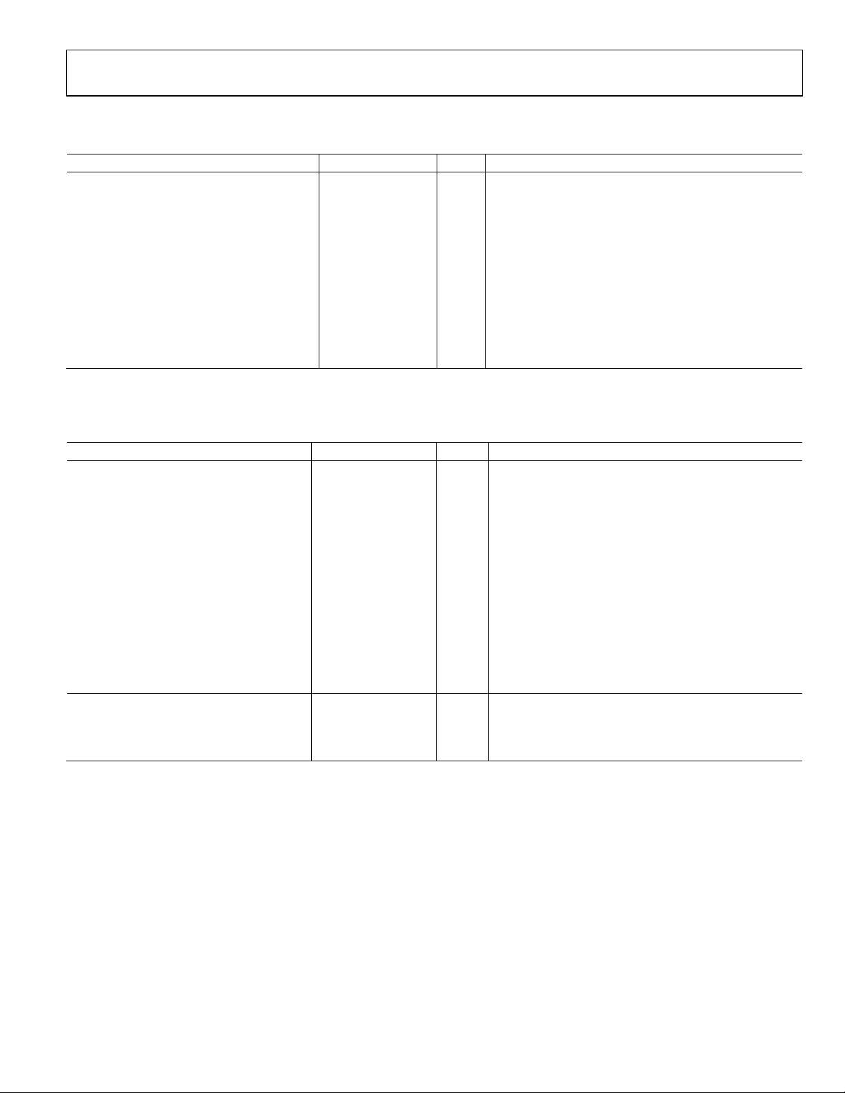
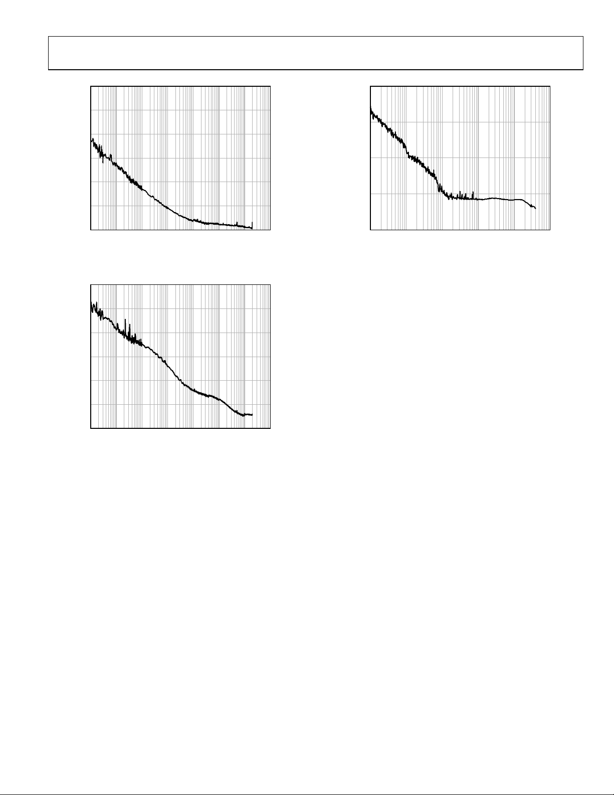
TYPICAL PERFORMANCE CHARACTERISTICS
350
3 CHANNELS—6 LVPECL
5
300
250
200
CURRENT (mA)
150
100
0 500 1000 1500 2000 2500 3000
3 CHANNELS—3 LVPECL
2 CHANNELS—2 LVPECL
1 CHANNEL—1 LVPECL
FREQUENCY (MHz )
Figure 6. Total Current vs. Frequency, CLK-to-Output (PLL Off),
LVPECL Outputs Terminated 50 Ω to VS_DRV − 2 V
240
220
200
180
160
140
CURRENT (mA)
120
100
80
0 50 100 150 200 250
3 CHANNELS—6 CMOS
3 CHANNELS—3 CMOS
2 CHANNELS—2 CMOS
1 CHANNEL—1 CMOS
FREQUENCY (MHz)
Figure 7. Total Current vs. Frequency, CLK-to-Output (PLL Off),
CMOS Outputs with 10 pF Load
5
4
PUMP DOWN PUMP UP
3
2
CURRENT FROM CP P IN (mA)
1
0
054.03.0 4.53.52.52.01.51.00.5
07239-108
VOLTAGE ON CP PIN (V)
.0
07239-112
Figure 9. Charge Pump Characteristics @ VCP = 5.0 V
140
–145
–150
–155
(dBc/Hz)
–160
–165
PFD PHASE NOI SE REFERRED TO PFD INPUT
–170
0.1 1 10010
07239-109
PFD FREQUENCY (MHz)
07239-013
Figure 10. PFD Phase Noise Referred to PFD Input vs. PFD Frequency
208
4
PUMP UPPUMP DOWN
3
2
CURRENT FROM CP P IN (mA)
1
0
033.02.52.01.51.00.5
VOLTAGE ON CP PIN (V)
Figure 8. Charge Pump Characteristics @ VCP = 3.3 V
–210
–212
–214
–216
–218
–220
PLL FIGURE OF MERIT (dBc/ Hz)
–222
.5
07239-111
–224
DIFFERENTIAL INPUT
SINGLE- ENDED INPUT
0 0.4 0.8 1.20.2 0.6 1.0 1.4
INPUT SLEW RATE (V/ns)
Figure 11. PLL Figure of Merit (FOM) vs. Slew Rate at REFIN/
Rev. 0 | Page 20 of 80
07239-114
REFIN
AD9520-5
http://www.BDTIC.com/ADI
3.5
3.0
VS_DRV = 3.135V
2.5
VS_DRV = 2.35V
2.0
(V)
OH
V
1.5
1.0
0.5
0
10k 1k 100
RESISTIVE LOAD (Ω)
Figure 12. CMOS Output VOH (Static) vs. R
VS_DRV = 3.3V
VS_DRV = 2.5V
LOAD
(to Ground)
1.2
0.8
0.4
0
–0.4
DIFFERENTIAL OUTPUT (V)
–0.8
–1.2
02222018161412108642
TIME (ns)
Figure 13. LVPECL Output (Differential) @ 100 MHz
1.0
07239-118
4
07239-014
3.2
2.8
2.4
2.0
1.6
AMPLITUDE ( V)
1.2
0.8
0.4
0
0860 1004020 7050 903010
TIME (ns)
0
Figure 15. CMOS Output with 10 pF Load @ 25 MHz
3.2
2.8
2.4
2.0
1.6
AMPLITUDE (V)
1.2
0.8
0.4
0
01987654321
2pF LOAD
TIME (ns)
10pF
LOAD
Figure 16. CMOS Output with 2 pF and 10 pF Load @ 250 MHz
2.0
07239-018
0
07239-019
0.6
0.2
–0.2
DIFFERENTIAL SWING (V p-p)
–0.6
–1.0
010.5 1.0
TIME (ns)
Figure 14. LVPECL Differential Voltage Swing @ 1600 MHz
1.8
1.6
1.4
DIFFERENTIAL SWING (V p-p)
1.2
.5
07239-015
1.0
031.5 2. 0 2.51.00.5
FREQUENCY (GHz)
Figure 17. LVPECL Differential Voltage Swing vs. Frequency
Rev. 0 | Page 21 of 80
.0
07239-123
AD9520-5
–
–
–
http://www.BDTIC.com/ADI
4.0
100
3.5
3.0
2.5
2.0
1.5
AMPLITUDE (V)
1.0
0.5
0
07
FREQUENCY (MHz )
2pF
10pF
20pF
600500400300200100
00
07239-124
Figure 18. CMOS Output Swing vs. Frequency and Capacitive Load
–110
–120
–130
–140
PHASE NOISE (dBc/Hz)
–150
–160
10 1k100 100M1M 10M100k10k
Figure 20. Additive (Residual) Phase Noise, CLK-to-LVPECL @
100
–110
–120
–130
–140
PHASE NOISE (dBc/Hz)
–150
110
–120
–130
–140
–150
PHASE NOISE (dBc/Hz)
–160
FREQUENCY (Hz)
1600 MHz, Divide-by-1
07239-130
–160
10 1k100 100M1M 10M100k10k
FREQUENCY (Hz)
Figure 19. Additive (Residual) Phase Noise, CLK-to-LVPECL @
245.76 MHz, Divide-by-1
–170
10 1k100 100M1M 10M100k10k
07239-128
FREQUENCY (Hz)
07239-131
Figure 21. Additive (Residual) Phase Noise, CLK-to-CMOS @
50 MHz, Divide-by-20
Rev. 0 | Page 22 of 80
AD9520-5
–
–
–
http://www.BDTIC.com/ADI
100
–110
–120
120
–130
–130
–140
PHASE NOISE (dBc/Hz)
–150
–160
10 1k100 100M1M 10M100k10k
FREQUENCY (Hz)
Figure 22. Additive (Residual) Phase Noise, CLK-to-LVPECL @
200 MHz, Divide-by-5
100
–110
–120
–130
–140
PHASE NOISE (dBc/Hz)
–150
–160
10 1k100 100M1M 10M100k10k
FREQUENCY (Hz)
Figure 23. Additive (Residual) Phase Noise, CLK-to-CMOS @
250 MHz, Divide-by-4
–140
PHASE NOISE (dBc/Hz)
–150
–160
1k 100M1M 10M100k10k
07239-129
FREQUENCY (Hz)
07239-135
Figure 24. Phase Noise (Absolute), External VCXO (Toyocom TCO-2112)
@ 245.76 MHz; PFD = 15.36 MHz; LBW = 250 Hz; LVPECL Output = 245.76 MHz
07239-132
Rev. 0 | Page 23 of 80

AD9520-5
http://www.BDTIC.com/ADI
TERMINOLOGY
Phase Jitter and Phase Noise
An ideal sine wave can be thought of as having a continuous
and even progression of phase with time from 0° to 360° for
each cycle. Actual signals, however, display a certain amount
of variation from ideal phase progression over time. This
phenomenon is called phase jitter. Although many causes can
contribute to phase jitter, one major cause is random noise,
which is characterized statistically as being Gaussian (normal)
in distribution.
This phase jitter leads to a spreading out of the energy of the
sine wave in the frequency domain, producing a continuous
power spectrum. This power spectrum is usually reported as a
series of values whose units are dBc/Hz at a given offset in
frequency from the sine wave (carrier). The value is a ratio
(expressed in decibels) of the power contained within a 1 Hz
bandwidth with respect to the power at the carrier frequency.
For each measurement, the offset from the carrier frequency is
also given.
It is meaningful to integrate the total power contained within
some interval of offset frequencies (for example, 10 kHz to
10 MHz). This is called the integrated phase noise over that
frequency offset interval and can be readily related to the time
jitter due to the phase noise within that offset frequency interval.
Phase noise has a detrimental effect on the performance of ADCs,
DACs, and RF mixers. It lowers the achievable dynamic range of
the converters and mixers, although they are affected in somewhat
different ways.
Time Jitter
Phase noise is a frequency domain phenomenon. In the time
domain, the same effect is exhibited as time jitter. When observing
a sine wave, the time of successive zero crossings varies. In a square
wave, the time jitter is a displacement of the edges from their
ideal (regular) times of occurrence. In both cases, the variations in
timing from the ideal are the time jitter. Because these variations
are random in nature, the time jitter is specified in seconds root
mean square (rms) or 1 sigma of the Gaussian distribution.
Time jitter that occurs on a sampling clock for a DAC or an
ADC decreases the signal-to-noise ratio (SNR) and dynamic
range of the converter. A sampling clock with the lowest possible
jitter provides the highest performance from a given converter.
Additive Phase Noise
Additive phase noise is the amount of phase noise that is
attributable to the device or subsystem being measured.
The phase noise of any external oscillators or clock sources is
subtracted. This makes it possible to predict the degree to which
the device impacts the total system phase noise when used in
conjunction with the various oscillators and clock sources, each
of which contributes its own phase noise to the total. In many
cases, the phase noise of one element dominates the system
phase noise. When there are multiple contributors to phase
noise, the total is the square root of the sum of squares of the
individual contributors.
Additive Time Jitter
Additive time jitter is the amount of time jitter that is attributable to
the device or subsystem being measured. The time jitter of any
external oscillators or clock sources is subtracted. This makes it
possible to predict the degree to which the device impacts the
total system time jitter when used in conjunction with the various
oscillators and clock sources, each of which contributes its own
time jitter to the total. In many cases, the time jitter of the external
oscillators and clock sources dominates the system time jitter.
Rev. 0 | Page 24 of 80
AD9520-5
V
http://www.BDTIC.com/ADI
DETAILED BLOCK DIAGRAM
OPTIONAL
REFIN
REFIN
REF1
REF2
REF_SEL CPRSETVCP
REFERENCE
SWITCHOVER
STATUS
STATUS
BUF
AMP
S GND RSET
DISTRIBUTION
REFERENCE
CLOCK
DOUBLER
STATUS
P, P + 1
PRESCALER
N DIVIDER
ZERO DELAY BL OCK
A/B
COUNTERS
REFMON
R
DIVIDE R
PROGRAMMABLE
PROGRAMMABLE
N DELAY
R DELAY
LOCK
DETECT
PHASE
FREQUENCY
DETECTOR
PLL
REFERENCE
CHARGE
PUMP
LD
HOLD
CP
STATUS
CLK
CLK
PD
SYNC
RESET
EEPROM
SP1
SP0
SCLK/SCL
SDIO/SDA
SDO
CS
DIGITAL
LOGIC
SERIAL
PORT
DECODE
INTERFACE
SPI
EEPROM
INTERFACE
I2C
DIVIDE BY 1,
2, 3, 4, 5, OR 6
01
DIVIDE BY
1 TO 32
DIVIDE BY
1 TO 32
DIVIDE BY
1 TO 32
VS_DRV
OUT0
OUT0
OUT1
OUT1
OUT2
OUT2
OUT3
OUT3
OUT4
OUT4
OUT5
OUT5
OUT6
OUT6
LVPECL/CMOS OUTPUT
OUT7
OUT7
OUT8
OUT8
AD9520-5
DIVIDE BY
1 TO 32
Figure 25.
Rev. 0 | Page 25 of 80
OUT9
OUT9
OUT10
OUT10
OUT11
OUT11
07239-028

AD9520-5
http://www.BDTIC.com/ADI
THEORY OF OPERATION
OPERATIONAL CONFIGURATIONS
The AD9520 can be configured in several ways. These
configurations must be set up by loading the control registers
(see Tabl e 44 to Ta ble 55). Each section or function must be
individually programmed by setting the appropriate bits in the
corresponding control register or registers. When the desired
configuration is programmed, the user can store these values in
the on-board EEPROM to allow the part to power up in the desired
configuration without user intervention.
Mode 1: Clock Distribution or External VCO < 1600 MHz
When the external clock source to be distributed or the external
VCO/VCXO is <1600 MHz, a configuration that bypasses the
VCO divider can be used. This is the only difference from Mode 2.
Bypassing the VCO divider limits the frequency of the clock
source to <1600 MHz (due to the maximum input frequency
allowed at the channel dividers).
Configuration and Register Settings
For clock distribution applications where the external clock is
<1600 MHz, the register settings shown in Tab l e 1 9 should be used.
Table 19. Settings for Clock Distribution < 1600 MHz
Register Description
0x010[1:0] = 01b PLL asynchronous power-down (PLL off )
0x1E1[0] = 1b
0x1E1[1] = 0b CLK selected as the source
Bypass the VCO divider as the source for
the distribution section
When using the internal PLL with an external VCO < 1600 MHz,
the PLL must be turned on.
Table 20. Settings for Using Internal PLL with External VCO
< 1600 MHz
Register Description
0x1E1[0] = 1b
0x010[1:0] = 00b
An external VCO/VCXO requires an external loop filter that
must be connected between CP and the tuning pin of the VCO/
VCXO. This loop filter determines the loop bandwidth and stability
of the PLL. Make sure to select the proper PFD polarity for the
VCO/VCXO being used.
Table 21. Setting the PFD Polarity
Register Description
0x010[7] = 0b
0x010[7] = 1b
Bypass the VCO divider as the source for
the distribution section
PLL normal operation (PLL on) along
with other appropriate PLL settings in
0x010 to 0x01E
PFD polarity positive (higher control voltage
produces higher frequency)
PFD polarity negative (higher control voltage
produces lower frequency)
Rev. 0 | Page 26 of 80

AD9520-5
V
http://www.BDTIC.com/ADI
OPTIONAL
REFIN
REFIN
CLK
CLK
PD
SYNC
RESET
EEPROM
REF1
REF2
DIGITAL
REF_SEL CPRSETVCP
REFERENCE
SWITCHOVER
STATUS
STATUS
BUF
AMP
LOGIC
EEPROM
S GND RSET
DISTRIBUTION
REFERENCE
CLOCK
DOUBLER
STATUS
P, P + 1
PRESCALER
N DIVIDER
ZERO DELAY BL OCK
DIVIDE BY 1,
2, 3, 4, 5, OR 6
01
A/B
COUNTERS
REFMON
R
DIVIDE R
PROGRAMMABLE
N DELAY
DIVIDE BY
1 TO 32
LOCK
DETECT
R DELAY
PROGRAMMABLE
PHASE
FREQUENCY
DETECTOR
PLL
REFERENCE
CHARGE
PUMP
LD
HOLD
CP
STATUS
VS_DRV
OUT0
OUT0
OUT1
OUT1
OUT2
OUT2
OUT3
SP1
SP0
SCLK/SCL
SDIO/SDA
SDO
CS
SERIAL
PORT
DECODE
INTERFACE
SPI
I2C
INTERFACE
AD9520-5
DIVIDE BY
1 TO 32
DIVIDE BY
1 TO 32
DIVIDE BY
1 TO 32
OUT3
OUT4
OUT4
OUT5
OUT5
OUT6
OUT6
OUT7
OUT7
OUT8
OUT8
OUT9
OUT9
OUT10
OUT10
OUT11
OUT11
LVPECL/CMOS OUTPUT
07239-031
Figure 26. Clock Distribution or External VCO < 1600 MHz (Mode 1)
Rev. 0 | Page 27 of 80
AD9520-5
http://www.BDTIC.com/ADI
Mode 2: High Frequency Clock Distribution—CLK or External VCO > 1600 MHz
The AD9520 power-up default configuration has the PLL
powered off and the routing of the input set so that the CLK/
CLK
input is connected to the distribution section through the
VCO divider (divide-by-1/divide-by-2/divide-by-3/divide-by-4/
divide-by-5/divide-by-6). This is a distribution-only mode that
allows for an external input up to 2400 MHz (see ). The
Table 3
maximum frequency that can be applied to the channel dividers
is 1600 MHz; therefore, higher input frequencies must be divided
down before reaching the channel dividers.
When the PLL is enabled, this routing also allows the use of the
PLL with an external VCO or VCXO with a frequency <2400 MHz.
In this configuration, the external VCO/VCXO feeds directly
into the prescaler.
The register settings shown in Table 2 2 are the default values of
these registers at power-up or after a reset operation.
Table 22. Default Register Settings for Clock Distribution Mode
Register Description
0x010[1:0] = 01b PLL asynchronous power-down (PLL off )
0x1E0[2:0] = 000b Set VCO divider = 2
0x1E1[0] = 0b Use the VCO divider
When using the internal PLL with an external VCO, the PLL
must be turned on.
Table 23. Settings When Using an External VCO
Register Description
0x010[1:0] = 00b PLL normal operation (PLL on)
0x010 to 0x01E
PLL settings; select and enable a
reference input; set R, N (P, A, B), PFD
polarity, and I
loop configuration
according to the intended
CP
An external VCO requires an external loop filter that must be
connected between CP and the tuning pin of the VCO. This
loop filter determines the loop bandwidth and stability of the
PLL. Make sure to select the proper PFD polarity for the VCO
being used.
Table 24. Setting the PFD Polarity
Register Description
0x010[7] = 0b
0x010[7] = 1b
PFD polarity positive (higher control
voltage produces higher frequency)
PFD polarity negative (higher control
voltage produces lower frequency)
Rev. 0 | Page 28 of 80

AD9520-5
V
http://www.BDTIC.com/ADI
OPTIONAL
REFIN
REFIN
CLK
CLK
PD
SYNC
RESET
EEPROM
REF1
REF2
DIGITAL
REF_SEL CPRSETVCP
REFERENCE
SWITCHOVER
STATUS
STATUS
BUF
AMP
LOGIC
EEPROM
S GND RSET
DISTRIBUTI ON
REFERENCE
CLOCK
DOUBLER
STATUS
P, P + 1
PRESCALER
N DIVIDER
ZERO DELAY BL OCK
DIVIDE BY 1,
2, 3, 4, 5, OR 6
01
A/B
COUNTERS
REFMO N
R
DIVIDER
PROGRAMMABLE
N DELAY
DIVIDE BY
1 TO 32
LOCK
DETECT
R DELAY
PROGRAMMABLE
PHASE
FREQUENCY
DETECT OR
PLL
REFERENCE
CHARGE
PUMP
LD
HOLD
CP
STATUS
VS_DRV
OUT0
OUT0
OUT1
OUT1
OUT2
OUT2
OUT3
SP1
SP0
SCLK/SCL
SDIO/SDA
SDO
CS
SERIAL
PORT
DECODE
INTERFACE
SPI
I2C
INTERFACE
AD9520-5
DIVIDE BY
1 TO 32
DIVIDE BY
1 TO 32
DIVIDE BY
1 TO 32
OUT3
OUT4
OUT4
OUT5
OUT5
OUT6
OUT6
OUT7
OUT7
OUT8
OUT8
OUT9
OUT9
OUT10
OUT10
OUT11
OUT11
LVPECL/CMOS O UTPUT
07239-029
Figure 27. High Frequency Clock Distribution or External VCO > 1600 MHz (Mode 2)
Rev. 0 | Page 29 of 80

AD9520-5
V
http://www.BDTIC.com/ADI
Phase-Locked Loop (PLL)
S GND RSET
DISTRI BUTION
REFERENCE
CLOCK
DOUBLER
STATUS
P, P + 1
PRESCALER
N DIVIDER
ZERO DELAY BL OCK
DIVIDE BY 1,
2, 3, 4, 5, OR 6
01
A/B
COUNTERS
Figure 28. PLL Functional Block Diagram
OPTIONAL
REFIN
REFIN
CLK
CLK
REF1
REF2
REF_SEL
REFERENCE
SWITCHOVER
STATUS
BUF
AMP
STATUS
The AD9520 includes on-chip PLL blocks that can be used with
an external VCO or VCXO to create a complete phase-locked
loop. The PLL requires an external loop filter, which usually
consists of a small number of capacitors and resistors. The
configuration and components of the loop filter help to
establish the loop bandwidth and stability of the PLL.
The AD9520 PLL is useful for generating clock frequencies
from a supplied reference frequency. This includes conversion
of reference frequencies to much higher frequencies for subsequent
division and distribution. In addition, the PLL can be used to
clean up jitter and phase noise on a noisy reference. The exact
choice of PLL parameters and loop dynamics is application specific.
The flexibility and depth of the AD9520 PLL allow the part to
be tailored to function in many different applications and signal
environments.
Configuration of the PLL
Configuration of the PLL is accomplished by programming
the various settings for the R divider, N divider, PFD polarity,
and charge pump current. The combination of these settings
determines the PLL loop bandwidth. These are managed through
programmable register settings (see Table 4 4 and Ta b le 4 8 ) and
by the design of the external loop filter.
Successful PLL operation and satisfactory PLL loop performance
are highly dependent on proper configuration of the PLL
settings, and the design of the external loop filter is crucial to
the proper operation of the PLL.
REFMON
LOCK
DETECT
R
DIVIDER
PROGRAMMABLE
N DELAY
FROM CHANNEL
DIVIDER 0
R DELAY
PROGRAMMABLE
PHASE
FREQUENCY
DETECTOR
ADIsimCLK™ is a free program that can help with the design
and exploration of the capabilities and features of the AD9520,
including the design of the PLL loop filter. The AD9516 model
found in ADIsimCLK Version 1.2 can also be used for modeling
the AD9520 loop filter. It is available at www.analog.com/clocks.
Phase Frequency Detector (PFD)
The PFD takes inputs from the R divider and the N divider and
produces an output proportional to the phase and frequency
difference between them. The PFD includes a programmable
delay element that controls the width of the antibacklash pulse.
This pulse ensures that there is no dead zone in the PFD
transfer function and minimizes phase noise and reference
spurs. The antibacklash pulse width is set by 0x017[1:0].
An important limit to keep in mind is the maximum frequency
allowed into the PFD. The maximum input frequency into the
PFD is a function of the antibacklash pulse setting, as specified
in the phase/frequency detector (PFD) parameter in Tabl e 2.
Charge Pump (CP)
The charge pump is controlled by the PFD. The PFD monitors
the phase and frequency relationship between its two inputs and
tells the CP to pump up or pump down to charge or discharge the
integrating node (part of the loop filter). The integrated and
filtered CP current is transformed into a voltage that drives the
tuning node of the external VCO to move the VCO frequency
up or down. The CP can be set (0x010[3:2]) for high impedance
(allows holdover operation), for normal operation (attempts to
lock the PLL loop), for pump-up, or for pump-down (test modes).
The CP current is programmable in eight steps from (nominally)
0.6 mA to 4.8 mA. The exact value of the CP current LSB is set
by the CPRSET resistor, which is nominally 5.1 kΩ.
CPRSETVCP
PLL
REFERENCE
CHARGE
PUMP
HOLD
LD
CP
STATUS
VS_DRV
07239-064
Rev. 0 | Page 30 of 80

AD9520-5
V
http://www.BDTIC.com/ADI
PLL External Loop Filter
An example of an external loop filter for the PLL is shown in
Figure 29. A loop filter must be calculated for each desired PLL
configuration. The values of the components depend on the VCO
frequency, the K
, the PFD frequency, the charge pump current,
VCO
the desired loop bandwidth, and the desired phase margin. The
loop filter affects the phase noise, the loop settling time, and the
loop stability. A basic knowledge of PLL theory is necessary for
understanding loop filter design. ADIsimCLK can help with the
calculation of a loop filter according to the application requirements.
AD9520-5
CLK/CLK
CP
CHARGE
PUMP
Figure 29. Example of External Loop Filter for PLL
EXTERNAL
VCO/VCXO
R2
R1
C1 C2 C3
07239-065
PLL Reference Inputs
The AD9520 features a flexible PLL reference input circuit that
allows a fully differential input, two separate single-ended inputs,
or a 16.67 MHz to 33.33 MHz crystal oscillator with an on-chip
maintaining amplifier. An optional reference clock doubler
can be used to double the PLL reference frequency. The input
frequency range for the reference inputs is specified in Table 2 .
Both the differential and the single-ended inputs are self-biased,
allowing for easy ac coupling of input signals.
Either a differential or a single-ended reference must be specifically
enabled. All PLL reference inputs are off by default.
The differential input and the single-ended inputs share two pins,
REFIN (REF1) and
REFIN
(REF2). The desired reference input
type is selected and controlled by 0x01C (see and ). Ta ble 44 Tab le 48
When the differential reference input is selected, the self-bias
level of the two sides is offset slightly to prevent chattering of
the input buffer when the reference is slow or missing. The
specification for this voltage level can be found in Ta b le 2 .
The input hysteresis increases the voltage swing required of
the driver to overcome the offset.
The single-ended inputs can be driven by either a dc-coupled
CMOS level signal or an ac-coupled sine wave or square wave. To
avoid input buffer chatter when a single-ended, ac-coupled input
signal stops toggling, the user can set 0x018[7] to 1b. This shifts the
dc offset bias point down 140 mV. To increase isolation and reduce
power, each single-ended input can be independently powered down.
The differential reference input receiver is powered down when
the differential reference input is not selected or when the PLL
is powered down. The single-ended buffers power down when
the PLL is powered down or when their respective individual
power-down registers are set. When the differential mode is
selected, the single-ended inputs are powered down.
In differential mode, the reference input pins are internally selfbiased so that they can be ac-coupled via capacitors. It is possible to
dc couple to these inputs. If the differential REFIN is driven by
a single-ended signal, the unused side (
decoupled via a suitable capacitor to a quiet ground.
REFIN
) should be
Figure 30
shows the equivalent circuit of REFIN.
S
85kΩ
REF1
VS
REFIN
REFIN
REF2
Figure 30. REFIN Equivalent Circuit for Non-XTAL Mode
10kΩ 12kΩ
150Ω
150Ω
10kΩ 10kΩ
VS
85kΩ
07239-066
Crystal mode is nearly identical to differential mode. The user
enables a maintaining amplifier by setting the Enable XTAL
OSC bit, and putting a series resonant, AT fundamental cut
crystal across the REFIN/
REFIN
pins.
Reference Switchover
The AD9520 supports dual single-ended CMOS inputs, as well
as a single differential reference input. In the dual single-ended
reference mode, the AD9520 supports automatic and manual
PLL reference clock switching between REF1 (on Pin REFIN)
and REF2 (on Pin
REFIN
). This feature supports networking
and other applications that require redundant references.
The AD9520 features a dc offset option in single-ended mode.
This option is designed to eliminate the risk of the reference
inputs chattering when they are ac-coupled and the reference
clock disappears. When using the reference switchover, the
single-ended reference inputs should be dc-coupled CMOS
levels (with the AD9520 dc offset feature disabled). Alternatively,
the inputs can be ac-coupled and the dc offset feature enabled.
The user should keep in mind, however, that the minimum
input amplitude for the reference inputs is greater when the dc
offset is turned on.
Rev. 0 | Page 31 of 80

AD9520-5
http://www.BDTIC.com/ADI
There are several configurable modes of reference switchover.
The switchover can be performed manually or automatically.
Manual switchover is performed either through Register 0x01C
or by using the REF_SEL pin. The automatic switchover occurs
when REF1 disappears. There is also a switchover deglitch feature
which ensures that the PLL does not receive rising edges that are far
out of alignment with the newly selected reference.
There are two automatic reference switchover modes (0x01C):
• Prefer REF1. Switch from REF1 to REF2 when REF1 disappears.
Return to REF1 from REF2 when REF1 returns.
• Stay on REF2. Automatically switch to REF2 when REF1
disappears, but do not switch back to REF1 when it reappears.
The reference can be set back to REF1 manually at an
appropriate time.
In automatic mode, REF1 is monitored by REF2. If REF1
disappears (two consecutive falling edges of REF2 without an
edge transition on REF1), REF1 is considered missing. On the
next subsequent rising edge of REF2, REF2 is used as the reference
clock to the PLL. If 0x01C[3] = 0b (default), when REF1 returns
(four rising edges of REF1 without two falling edges of REF2
between the REF1 edges), the PLL reference switches back to
REF1. If 0x01C[3] = 1b, the user can control when to switch
back to REF1. This is done by programming the part to manual
reference select mode (0x01C[4] = 0b) and by ensuring that the
registers and/or the REF_SEL pin is set to select the desired
reference. Automatic mode can be reenabled when REF1 is
reselected.
Manual switchover requires the presence of a clock on the reference
input that is being switched to or that the deglitching feature be
disabled (0x01C[7]).
Reference Divider R
The reference inputs are routed to the reference divider, R. R (a
14-bit counter) can be set to any value from 0 to 16,383 by writing
to 0x011 and 0x012. (Both R = 0 and R = 1 give divide-by-1.) The
output of the R divider goes to one of the PFD inputs to be
compared with the VCO frequency divided by the N divider.
The frequency applied to the PFD must not exceed the maximum
allowable frequency, which depends on the antibacklash pulse
setting (see Tab l e 2 ).
The R divider has its own reset. The R divider can be reset using
the shared reset bit of the R, A, and B counters. It can also be
reset by a
SYNC
operation.
VCO/VCXO Feedback Divider N: P, A, B, R
The N divider is a combination of a prescaler (P) and two counters,
A and B. The total divider value is
N = (P × B) + A
where P can be 2, 4, 8, 16, or 32.
Rev. 0 | Page 32 of 80
Prescaler
The prescaler of the AD9520 allows for two modes of operation:
a fixed divide (FD) mode of 1, 2, or 3, and a dual modulus
(DM) mode where the prescaler divides by P and (P + 1) {2 and
3, 4 and 5, 8 and 9, 16 and 17, or 32 and 33}. The prescaler
modes of operation are given in Tabl e 48 , 0x016[2:0]. Not all
modes are available at all frequencies (see Ta ble 2).
When operating the AD9520 in dual modulus mode, P/(P + 1),
the equation used to relate the input reference frequency to the
VCO output frequency is
f
= (f
VCO
/R) × (P × B + A) = f
REF
× N/R
REF
However, when operating the prescaler in FD Mode 1,
FD Mode 2, or FD Mode 3, the A counter is not used (A = 0)
and the equation simplifies to
f
= (f
VCO
/R) × (P × B) = f
REF
× N/R
REF
When A = 0, the divide is a fixed divide of P = 2, 4, 8, 16, or 32.
By using combinations of DM and FD modes, the AD9520 can
achieve values of N all the way down to N = 1. Table 25 shows
how a 10 MHz reference input can be locked to any integer
multiple of N.
Note that the same value of N can be derived in different ways,
as illustrated by the case of N = 12. The user can choose a fixed
divide mode P = 2 with B = 6, use the dual modulus mode 2/3
with A = 0, B = 6, or use the dual modulus mode 4/5 with
A = 0, B = 3.
A and B Counters
The B counter must be ≥3 or bypassed, and unlike the R
counter, A = 0 is actually zero.
The maximum input frequency to the A/B counter is reflected
in the maximum prescaler output frequency (~300 MHz) specified
in Tabl e 2. This is the prescaler input frequency (external VCO
or CLK) divided by P. For example, dual modulus P = 8/9 mode
is not allowed if the external VCO frequency is greater than
2400 MHz because the frequency going to the A/B counter is
too high.
When the AD9520 B counter is bypassed (B = 1), the A counter
should be set to zero, and the overall resulting divide is equal to
the prescaler setting, P. The possible divide ratios in this mode
are 1, 2, 3, 4, 8, 16, and 32.
Although manual reset is not normally required, the A/B counters
have their own reset bit. Alternatively, the A and B counters can be
reset using the shared reset bit of the R, A, and B counters. Note
that these reset bits are not self-clearing.
R, A, and B Counters:
SYNC
Pin Reset
The R, A, and B counters can be reset simultaneously through the
SYNC
pin. This function is controlled by 0x019[7:6] (see ).
SYNC
The
pin reset is disabled by default.
Tabl e 48

AD9520-5
http://www.BDTIC.com/ADI
R and N Divider Delays
Both the R and N dividers feature a programmable delay cell.
These delays can be enabled to allow adjustment of the phase
relationship between the PLL reference clock and the VCO or
CLK. Each delay is controlled by three bits. The total delay
range is about 1 ns. See 0x019 in Tab le 2 and Table 4 8.
Digital Lock Detect (DLD)
By selecting the proper output through the mux on each pin, the
DLD function is available at the LD, STATUS, and REFMON pins.
The digital lock detect circuit indicates a lock when the time
difference of the rising edges at the PFD inputs is less than a
specified value (the lock threshold). The loss of a lock is indicated
when the time difference exceeds a specified value (the unlock
threshold). Note that the unlock threshold is wider than the
lock threshold, which allows some phase error in excess of the
lock window to occur without chattering on the lock indicator.
The lock detect window timing depends on the value of the
CPRSET resistor, as well as three settings: the digital lock
detect window bit (0x018[4]), the antibacklash pulse width
bit (0x017[1:0], see Tabl e 2), and the lock detect counter
(0x018[6:5]). The lock and unlock detection values in Table 2
are for the nominal value of CPRSET = 5.11 k. Doubling the
CPRSET value to 10 k doubles the values in Tab le 2.
A lock is not indicated until there is a programmable number of
consecutive PFD cycles with a time difference less than the lock
detect threshold. The lock detect circuit continues to indicate a
lock until a time difference greater than the unlock threshold
occurs on a single subsequent cycle. For the lock detect to work
properly, the period of the PFD frequency must be greater than
the unlock threshold. The number of consecutive PFD cycles
required for a lock is programmable (0x018[6:5]).
Note that it is possible in certain low (<500 Hz) loop bandwidth,
high phase margin cases that the DLD can chatter during acquisition, which can cause the AD9520 to automatically enter and exit
holdover. To avoid this problem, it is recommended that the
user make provisions for a capacitor to ground on the LD pin so
that current source digital lock detect (CSDLD) mode can be used.
Table 25. How a 10 MHz Reference Input Can Be Locked to Any Integer Multiple of N
f
(MHz) R P A B N f
REF
10 1 1 X
10 1 2 X
10 1 1 X
10 1 1 X
10 1 1 X
10 1 2 X
1
1 1 10 FD P = 1, B = 1 (bypassed)
1
1 2 20 FD P = 2, B = 1 (bypassed)
1
3 3 30 FD P = 1, B = 3
1
4 4 40 FD P = 1, B = 4
1
5 5 50 FD P = 1, B = 5
1
3 6 60 FD P = 2, B = 3
(MHz) Mode Notes
VCO
10 1 2 0 3 6 60 DM P and P + 1 = 2 and 3, A = 0, B = 3
10 1 2 1 3 7 70 DM P and P + 1 = 2 and 3, A = 1, B = 3
10 1 2 2 3 8 80 DM P and P + 1 = 2 and 3, A = 2, B = 3
10 1 2 1 4 9 90 DM P and P + 1 = 2 and 3, A = 1, B = 4
10 1 2 X
1
5 10 100 FD P = 2, B = 5
10 1 2 0 5 10 100 DM P and P + 1 = 2 and 3, A = 0, B = 5
10 1 2 1 5 11 110 DM P and P + 1 = 2 and 3, A = 1, B = 5
10 1 2 X
1
6 12 120 FD P = 2, B = 6
10 1 2 0 6 12 120 DM P and P + 1 = 2 and 3, A = 0, B = 6
10 1 4 0 3 12 120 DM P and P + 1 = 4 and 5, A = 0, B = 3
10 1 4 1 3 13 130 DM P and P + 1 = 4 and 5, A = 1, B = 3
1
X = don’t care.
Rev. 0 | Page 33 of 80
AD9520-5
V
CLKC
http://www.BDTIC.com/ADI
Analog Lock Detect (ALD)
The AD9520 provides an ALD function that can be selected for
use at the LD pin. There are two operating modes for ALD:
• N-channel open-drain lock detect. This signal requires a
pull-up resistor to the positive supply, VS. The output is
normally high with short, low going pulses. Lock is indicated
by the minimum duty cycle of the low going pulses.
• P-channel open-drain lock detect. This signal requires a
pull-down resistor to GND. The output is normally low with
short, high going pulses. Lock is indicated by the minimum
duty cycle of the high going pulses.
The analog lock detect function requires an RC filter to provide a
logic level indicating lock/unlock. The ADIsimCLK tool can be
used to help the user select the right passive component values
for ALD to ensure its correct operation.
S = 3.3V
AD9520
LD
ALD
Figure 31. Example of Analog Lock Detect Filter Using
N-Channel Open-Drain Driver
R2
V
R1
OUT
C
07239-067
Current Source Digital Lock Detect (CSDLD)
During the PLL locking sequence, it is normal for the DLD
signal to toggle a number of times before remaining steady
when the PLL is completely locked and stable. There may be
applications where it is desirable to have DLD asserted only
after the PLL is solidly locked. This is possible by using the
current source digital lock detect function.
The current source lock detect provides a current of 110 µA when
DLD is true and shorts to ground when DLD is false. If a capacitor
is connected to the LD pin, it charges at a rate determined by the
current source during the DLD true time but is discharged nearly
instantly when DLD is false. By monitoring the voltage at the
LD pin (top of the capacitor), LD = high happens only after the
DLD is true for a sufficiently long time. Any momentary DLD
false resets the charging. By selecting a properly sized capacitor,
it is possible to delay a lock detect indication until the PLL is
stably locked and the lock detect does not chatter.
To use current source digital lock detect, do the following:
• Place a capacitor to ground on the LD pin
• Set 0x01A[5:0] = 0x04
• Enable the LD pin comparator (0x01D[3] = 1)
The LD pin comparator senses the voltage on the LD pin, and
the comparator output can be made available at the REFMON
pin control (0x01B[4:0]) or the STATUS pin control (0x017[7:2]).
The internal LD pin comparator trip point and hysteresis are given
in Tabl e 14 . The voltage on the capacitor can also be sensed by
an external comparator connected to the LD pin. In this case,
enabling the on-board LD pin comparator is not necessary.
Rev. 0 | Page 34 of 80
The user can asynchronously enable individual clock outputs only
when CSDLD is high. To enable this feature, set the appropriate bits
in the enable output on the CSDLD registers (0x0FC and 0x0FD).
AD9520
110µA
C
V
OUT
CLK
07239-068
)
DLD
LD PIN
COMPARAT OR
Figure 32. Current Source Digital Lock Detect
LD
REFMON
OR
STATUS
External VCXO/VCO Clock Input (CLK/
This differential input is used to drive the AD9520 clock
distribution section. This input can receive up to 2.4 GHz.
The pins are internally self-biased, and the input signal should
be ac-coupled via capacitors.
CLOCK INPUT
STAGE
07239-032
The CLK/
VS
LK
2.5kΩ 2.5kΩ
5kΩ
5kΩ
Figure 33. CLK Equivalent Input Circuit
CLK
input can be used either as a distribution only
input (with the PLL off ) or as a feedback input for an external
VCO/VCXO using the internal PLL.
Holdover
The AD9520 PLL has a holdover function. Holdover is
implemented by placing the charge pump in a high impedance
state. This function is useful when the PLL reference clock is
lost. Holdover mode allows the external VCO to maintain a
relatively constant frequency even though there is no reference
clock. Without this function, the charge pump is placed into a
constant pump-up or pump-down state, resulting in a massive
VCO frequency shift. Because the charge pump is placed in a
high impedance state, any leakage that occurs at the charge
pump output or the VCO tuning node causes a drift of the VCO
frequency. This can be mitigated by using a loop filter that
contains a large capacitive component because this drift is
limited by the current leakage induced slew rate (I
LEAK
/C) of
the VCO control voltage.
SYNC
Both a manual holdover mode, using the
pin, and an
automatic holdover mode are provided. To use either function, the
holdover function must be enabled (0x01D[0]).

AD9520-5
http://www.BDTIC.com/ADI
External/Manual Holdover Mode
A manual holdover mode can be enabled that allows the user to
place the charge pump into a high impedance state when the
SYNC
pin is asserted low. This operation is edge sensitive, not
level sensitive. The charge pump enters a high impedance state
immediately. To take the charge pump out of a high impedance
state, take the
high impedance state synchronously with the next PFD rising
edge from the reference clock. This prevents extraneous charge
pump events from occurring during the time between
going high and the next PFD event. This also means that the
charge pump stays in a high impedance state if there is no
reference clock present.
The B counter (in the N divider) is reset synchronously with the
charge pump, leaving the high impedance state on the reference
path PFD event. This helps align the edges out of the R and N
dividers for faster settling of the PLL. Because the prescaler is
not reset, this feature works best when the B and R numbers are
close because this results in a smaller phase difference for the
loop to settle out.
SYNC
pin high. The charge pump then leaves the
SYNC
When using this mode, the channel dividers should be set to ignore
SYNC
the
are not set to ignore the
to put the part into holdover, the distribution outputs turn off.
The channel divider ignore SYNC function is found in 0x191[6],
0x194[6], 0x197[6], and 0x19A[6] for Channel Divider 0, Channel
Divider 1, Channel Divider 2, and Channel Divider 3, respectively.
pin (at least after an initial
SYNC
SYNC
event). If the dividers
pin, any time
SYNC
is taken low
Automatic/Internal Holdover Mode
When enabled, this function automatically puts the charge
pump into a high impedance state when the loop loses lock.
The assumption is that the only reason the loop loses lock is due
to the PLL losing the reference clock; therefore, the holdover
function puts the charge pump into a high impedance state to
maintain the VCO frequency as close as possible to the original
frequency before the reference clock disappeared.
A flowchart of the automatic/internal holdover function
operation is shown in Figure 34.
Rev. 0 | Page 35 of 80

AD9520-5
http://www.BDTIC.com/ADI
PLL ENABLED
DLD == LOW
YES
WAS
LD PIN == HIG H
WHEN DLD WENT
LOW?
YES
HIGH IMPEDANCE
CHARGE PUMP
YES
REFERENCE
EDGE AT PFD?
YES
NO
NO
LOOP OUT OF LOCK. DIGITAL LOCK
DETECT SIGNAL GOES LOW WHEN THE
LOOP LEAVES LOCK AS DETERMINED
BY THE PHASE DIFFERENCE AT THE
INPUT OF THE PFD.
NO
ANALOG LO CK DETECT PI N INDICATES
LOCK WAS PREV IOUSLY ACHI EVED.
(0x01D[3] = 1; USE L D PIN VOLTAGE
WITH HOLDOVER.
0x01D[3] = 0; IGNORE LD PIN VOLTAG E,
TREAT LD PIN AS ALWAYS HIGH.)
CHARGE PUMP IS MADE
HIGH IMPEDANCE.
PLL COUNTERS CONTINUE
OPERATING NORMALLY.
CHARGE PUMP REMAINS HI GH
IMPEDANCE UNTI L THE REFERENCE
RETURNS.
YES
RELEASE
CHARGE PUMP
HIGH IMPEDANCE
YES
NO
DLD == HIGH
Figure 34. Flowchart of Automatic/Internal Holdover Mode
The holdover function senses the logic level of the LD pin as a
condition to enter holdover. The signal at LD can be from the
DLD, ALD, or current source LD mode (CSDLD). It is possible
to disable the LD comparator (0x01D[3]), which causes the
holdover function to always sense LD as being high. If DLD is
used, it is possible for the DLD signal to chatter while the PLL is
reacquiring lock. The holdover function may retrigger, thereby
preventing the holdover mode from terminating. Use of the
current source lock detect mode is recommended to avoid this
situation (see the Current Source Digital Lock Detect (CSDLD)
section).
TAKE CHARGE PUMP OUT OF
HIGH IMPEDANCE. PLL CAN
NOW RESET TLE.
WAIT FO R DLD TO G O HIGH. T HIS TAKES
5 TO 255 CYCLE S (PROGRAMMING OF T HE DLD
DELAY COUNTER) WITH THE REFERENCE AND
FEEDBACK CLOCKS I NSIDE THE L OCK WINDOW AT
THE PFD. THIS ENSURES THAT THE HOLDOVER
FUNCTION WAITS FOR THE PLL TO SETTLE AND LOCK
BEFORE THE HO LDOVER FUNCTION CAN BE
RETRIGG ERED.
When in holdover mode, the charge pump stays in a high
impedance state as long as there is no reference clock present.
As in the external holdover mode, the B counter (in the N divider)
is reset synchronously with the charge pump leaving the high
impedance state on the reference path PFD event. This helps
align the edges out of the R and N dividers for faster settling of
the PLL and reduces frequency errors during settling. Because
the prescaler is not reset, this feature works best when the B and
R numbers are close because this results in a smaller phase
difference for the loop to settle out.
7239-069
Rev. 0 | Page 36 of 80

AD9520-5
V
http://www.BDTIC.com/ADI
After leaving holdover, the loop then reacquires lock, and the
LD pin must go high (if 0x01D[3] = 1) before it can reenter
holdover.
The holdover function always responds to the state of the
currently selected reference (0x01C). If the loop loses lock
during a reference switchover (see the Reference Switchover
section), holdover is triggered briefly until the next reference
clock edge at the PFD.
The following registers affect the automatic/internal holdover
function:
• 0x018[6:5]—lock detect counter. This changes how many
consecutive PFD cycles with edges inside the lock detect
window are required for the DLD indicator to indicate
lock. This impacts the time required before the LD pin can
begin to charge as well as the delay from the end of a
holdover event until the holdover function can be reengaged.
• 0x018[3]—disable digital lock detect. This bit must be set
to 0 to enable the DLD circuit. Internal/automatic holdover
does not operate correctly without the DLD function enabled.
• 0x01A[5:0]—lock detect pin control. Set this to 000100b to
put it in the current source lock detect mode if using the
LD pin comparator. Load the LD pin with a capacitor of an
appropriate value.
• 0x01D[3]—LD pin comparator enable. 1 = enable; 0 =
disable. When disabled, the holdover function always
senses the LD pin as high.
• 0x01D[1]—external holdover control.
• 0x01D[0]—holdover enable. If holdover is disabled, both
external and automatic internal holdover are disabled.
REF_SEL CPRSETVCP
S GND RSET
For example, if the user wants to configure automatic holdover with
• Automatic reference switchover, prefer REF1.
• Digital lock detect: five PFD cycles, high range window.
• Automatic holdover using the LD pin comparator.
The following registers are set (in addition to the normal PLL
registers):
• 0x018[6:5] = 00b; lock detect counter = five cycles.
• 0x018[4] = 0b; digital lock detect window = high range.
• 0x018[3] = 1b; disable DLD normal operation.
• 0x01A[5:0] = 000100b; program LD pin control to current
source lock detect mode.
• 0x01C[4] = 1b; enable automatic switchover.
• 0x01C[3] = 0b; prefer REF1.
• 0x01C[2:1] = 11b; enable REF1 and REF2 input buffers.
• 0x01D[3] = 1b; enable LD pin comparator.
• 0x01D[1] = 0b; disable external holdover mode and use
automatic/internal holdover mode.
• 0x01D[0] = 1b; enable holdover.
Frequency Status Monitors
The AD9520 contains three frequency status monitors that are
used to indicate if the PLL reference (or references in the case of
single-ended mode) and the VCO have fallen below a threshold
frequency. A diagram showing their location in the PLL is
shown in Figure 35.
The PLL reference monitors have two threshold frequencies:
normal and extended (see Tab le 1 4 ). The reference frequency
monitor thresholds are selected in 0x01F.
REFMON
OPTIONAL
REFIN
REFIN
CLK
CLK
REF1
REF2
REFERENCE
SWITCHOVER
STATUS
BUF
STATUS
DISTRIBUTI ON
REFERENCE
CLOCK
DOUBLER
CLK FREQUENCY ST ATUS
P, P + 1
PRESCALER
N DIVIDE R
ZERO DELAY BLOCK
DIVIDE BY 1,
2, 3, 4, 5, OR 6
01
A/B
COUNTERS
PROGRAMMABLE
FROM CHANNEL
DIVIDER 0
Figure 35. Reference and VCO Status Monitors
Rev. 0 | Page 37 of 80
R
DIVIDER
N DELAY
LOCK
DETECT
R DELAY
PROGRAMMABLE
PHASE
FREQUENCY
DETECTOR
PLL
REFERENCE
CHARGE
PUMP
HOLD
LD
CP
STATUS
VS_DRV
07239-070

AD9520-5
http://www.BDTIC.com/ADI
REFIN/
REFIN
CLK/CL K
DIVIDERRDELAY
DIVIDERNDELAY
REG 0x01E[1] = 1
MUX1
DIVIDE BY 1,
2, 3, 4, 5, OR 6
01
R
N
EXTERNAL VCXO
PFD CP
INTERNAL ZERO DELAY CLO CK FEEDBACK PATH
AD9520-5
CHANNEL DIVIDER 0
CHANNEL DIVIDER 1
CHANNEL DIVIDER 2
CHANNEL DIVIDER 3
LOOP
FILTER
OUT0 TO OUT2
OUT3 TO OUT5
OUT6 TO OUT8
OUT9 TO OUT11
Figure 36. Zero Delay Function
ZERO DELAY OPERATION
Zero delay operation aligns the phase of the output clocks with
the phase of the external PLL reference input.
The zero delay function of the AD9520-5 is achieved by feeding
the output of Channel Divider 0 back to the PLL N divider. In
Figure 36, the change in signal routing for zero delay mode is
shown in blue.
Set Register 0x01E[1] = 1b to select zero delay mode. In the zero
delay mode, the output of Channel Divider 0 is routed back to the
PLL (N divider) through Mux1 (feedback path shown in blue in
Figure 36). The PLL synchronizes the phase/edge of the output of
Channel Divider 0 with the phase/edge of the reference input.
07239-053
Because the channel dividers are synchronized to each other,
the outputs of the channel divider are synchronous with the
reference input. Both the R delay and the N delay inside the
PLL can be programmed to compensate for the propagation
delay from the output drivers and PLL components to minimize
the phase offset between the clock output and the reference
input to achieve zero delay.
Rev. 0 | Page 38 of 80
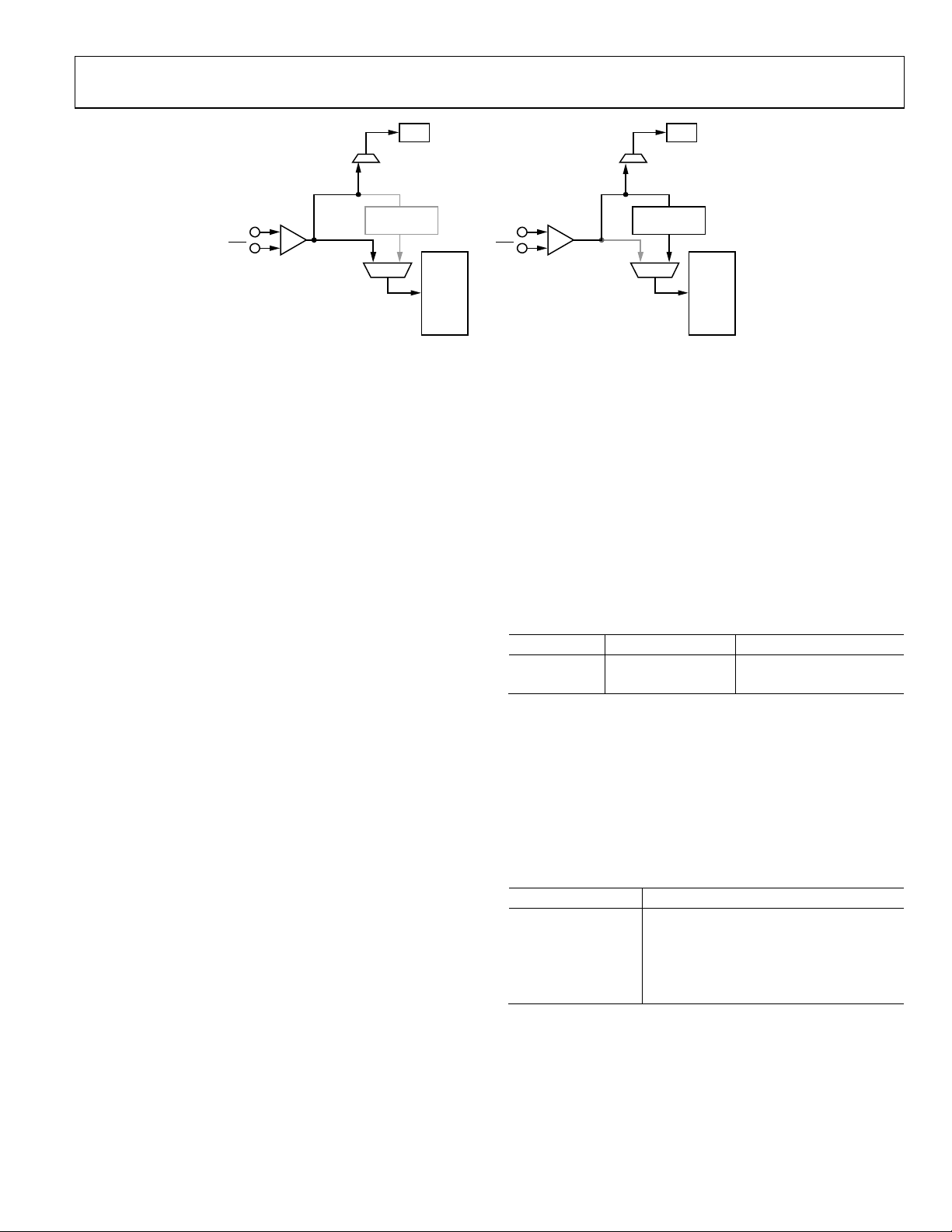
AD9520-5
http://www.BDTIC.com/ADI
PLL
PLL
DIVIDE BY 1,
CLK
CLK
MODE 1 (CLOCK DISTRIBUTION MODE)
Figure 37. Simplified Diagram of the Two Clock Distribution Operation Modes
2, 3, 4, 5, OR 6
01
DISTRI BUTION
CLOCK
CLOCK
DISTRI-
BUTION
CLOCK DISTRIBUTION
A clock channel consists of three LVPECL clock outputs or six
CMOS clock outputs that share a common divider. A clock
output consists of the drivers that connect to the output pins.
The clock outputs have either LVPECL or CMOS at the pins.
The AD9520 has four clock channels. Each channel has its own
programmable divider that divides the clock frequency applied
to its input. The channel dividers can divide by any integer from
1 to 32.
The AD9520 features a VCO divider that divides the CLK input by
1, 2, 3, 4, 5, or 6 before going to the individual channel dividers.
The VCO divider has two purposes. The first is to limit the
maximum input frequency of the channel dividers to 1.6 GHz.
The other is to allow the AD9520 to generate even lower
frequencies than would be possible with only a simple post divider.
The channel dividers allow for a selection of various duty cycles,
depending on the currently set division. That is, for any specific
division, D, the output of the divider can be set to high for N + 1
input clock cycles and low for M + 1 input clock cycles (where
D = N + M + 2). For example, a divide-by-5 can be high for one
divider input cycle and low for four cycles, or a divide-by-5 can
be high for three divider input cycles and low for two cycles.
Other combinations are also possible.
The channel dividers include a duty-cycle correction function
that can be disabled. In contrast to the selectable duty cycle
just described, this function can correct a non-50% duty cycle
caused by an odd division. However, this requires that the
division be set by M = N + 1.
In addition, the channel dividers allow a coarse phase offset or
delay to be set. Depending on the division selected, the output
can be delayed by up to 15 input clock cycles. For example, if
the frequency at the input of the channel divider is 1 GHz, the
channel divider output can be delayed by up to 15 ns. The
divider outputs can also be set to start high or to start low.
DIVIDE BY 1,
CLK
CLK
MODE 2 (HF CLOCK DISTRIBUTION MODE)
2, 3, 4, 5, OR 6
01
DISTRIBUTION
CLOCK
CLOCK
DISTRI-
BUTION
07239-054
Operation Modes
There are two clock distribution operating modes, and these are
shown in Figure 37.
It is not necessary to use the VCO divider if the CLK frequency
is less than the maximum channel divider input frequency
(1600 MHz); otherwise, the VCO divider must be used to
reduce the frequency going to the channel dividers.
Tabl e 26 shows how the operation modes are selected. 0x1E1[0]
selects the channel divider source.
Table 26. Operation Modes
Mode 0x1E1[0] VCO Divider
2 0 Used
1 1 Not used
CLK Direct-to-LVPECL Outputs
It is possible to connect the CLK directly to the LVPECL
outputs. However, the LVPECL outputs may not be able to meet
the V
specification in Tab l e 4 above 1600 MHz.
OD
To connect the LVPECL outputs directly to the CLK input, the
user must select the VCO divider as the source to the distribution
section, even if no channel uses it.
Table 27. Routing VCO Divider Input Directly to the Outputs
Register Setting Selection
0x1E1[0] = 0b CLK is the source; VCO divider selected
0x192[1] = 1b Direct-to-output OUT0, OUT1, OUT2
0x195[1] = 1b Direct-to-output OUT3, OUT4, OUT5
0x198[1] = 1b Direct-to-output OUT6, OUT7, OUT8
0x19B[1] = 1b Direct-to-output OUT9, OUT10, OUT11
Rev. 0 | Page 39 of 80

AD9520-5
http://www.BDTIC.com/ADI
Clock Frequency Division
The total frequency division is a combination of the VCO
divider (when used) and the channel divider. When the VCO
divider is used, the total division from the CLK to the output is
the product of the VCO divider (1, 2, 3, 4, 5, and 6) and the
division of the channel divider. Table 2 8 indicates how the
frequency division for a channel is set.
Table 28. Frequency Division
Channel
VCO Divider
Setting
1 to 6 Don’t care Enable 1
1 to 6 2 to 32 Disable (1 to 6) × (2 to 32)
2 to 6 Bypass Disable (2 to 6) × (1)
1 Bypass Disable
VCO divider
bypassed
VCO divider
bypassed
1
The bypass VCO divider (0x1E1[0] = 1) is not the same as VCO divider = 1.
Divider
1
Setting
Bypass Don’t care 1
2 to 32 Don’t care 2 to 32
CLK Directto-Output
Setting
Resulting
Frequency
Division
Output static
(illegal state)
The channel dividers feeding the output drivers contain one
2-to-32 frequency divider. This divider provides for division-by-1
to division-by-32. Division-by-1 is accomplished by bypassing
the divider. The dividers also provide for a programmable duty
cycle, with optional duty-cycle correction when the divide ratio
is odd. A phase offset or delay in increments of the input clock
cycle is selectable. The channel dividers operate with a signal at
their inputs up to 1600 MHz. The features and settings of the
dividers are selected by programming the appropriate setup
and control registers (see Tabl e 44 through Tab le 5 5 ).
VCO Divider
The VCO divider provides frequency division between the CLK
input and the clock distribution channel dividers. The VCO
divider can be set to divide by 1, 2, 3, 4, 5, or 6 (see Tabl e 51 ,
0x1E0[2:0]). However, when the VCO divider is set to 1, none
of the channel output dividers can be bypassed.
The VCO divider can also be set to static, which is useful for
applications where the only desired output frequency is the
CLK input frequency. Making the VCO divider static increases
the wide band spurious-free dynamic range (SFDR). An
alternative to achieving the same SFDR performance is to set
the VCO divider to 1 and enable CLK direct mode.
Channel Dividers
A channel divider drives each group of three LVPECL outputs.
There are four channel dividers (0, 1, 2, and 3) driving 12 LVPECL
outputs (OUT0 to OUT11). Tabl e 29 gives the register locations
used for setting the division and other functions of these dividers.
The division is set by the values of M and N. The divider can be
bypassed (equivalent to divide-by-1, divider circuit is powered
down) by setting the bypass bit. The duty-cycle correction can
be enabled or disabled according to the setting of the disable
divider DCC bits.
Table 29. Setting D
Di vider Low Cycles M High Cyc les N B ypass
0 0x190[7:4] 0x190[3:0] 0x191[7] 0x192[0]
1 0x193[7:4] 0x193[3:0] 0x194[7] 0x195[0]
2 0x196[7:4] 0x196[3:0] 0x197[7] 0x198[0]
3 0x199[7:4] 0x199[3:0] 0x19A[7] 0x19B[0]
for the Output Dividers
X
Disable
Div DCC
Channel Frequency Division (0, 1, 2, and 3)
For each channel (where the channel number x is 0, 1, 2, or 3),
the frequency division, D
, is set by the values of M and N
X
(four bits each, representing Decimal 0 to Decimal 15), where
Number of Low Cycles = M + 1
Number of High Cycles = N + 1
The high and low cycles are cycles of the clock signal currently
routed to the input of the channel dividers (VCO divider out
or CLK).
When a divider is bypassed, D
Otherwise, D
= (N + 1) + (M + 1) = N + M + 2. This allows
X
= 1.
X
each channel divider to divide by any integer from 1 to 32.
Duty Cycle and Duty-Cycle Correction
The duty cycle of the clock signal at the output of a channel is a
result of some or all of the following conditions:
• The M and N values for the channel
• DCC enabled/disabled
• VCO divider enabled/bypassed
• The CLK input duty cycle
The DCC function is enabled by default for each channel divider.
However, the DCC function can be disabled individually for
each channel divider by setting the disable divider DCC bit for
that channel.
Certain M and N values for a channel divider result in a non50% duty cycle. A non-50% duty cycle can also result with an
even division, if M ≠ N. The duty-cycle correction function
automatically corrects non-50% duty cycles at the channel
divider output to 50% duty cycle.
Duty-cycle correction requires the following channel divider
conditions:
• An even division must be set as M = N.
• An odd division must be set as M = N + 1.
When not bypassed or corrected by the DCC function, the duty
cycle of each channel divider output is the numerical value of
(N + 1)/(N + M + 2) expressed as a percent.
Rev. 0 | Page 40 of 80
AD9520-5
http://www.BDTIC.com/ADI
The duty cycle at the output of the channel divider for various
configurations is shown in Tabl e 30 to Ta bl e 33.
Table 30. Channel Divider Output Duty Cycle with VCO
Divider ≠ 1; Input Duty Cycle Is 50%
Output Duty Cycle
D
X
VCO
Divider
Even
Odd = 3
Odd = 5
Even, odd Even (N + 1)/(N + M + 2)
Even, odd Odd (N + 1)/(N + M + 2)
N + M + 2
Channel
divider
bypassed
Channel
divider
bypassed
Channel
divider
bypassed
Disable Div
DCC = 1
50% 50%
33.3% 50%
40% 50%
Disable Div
DCC = 0
50%, requires
M = N
50%, requires
M = N + 1
Table 31. Channel Divider Output Duty Cycle with VCO
Divider ≠ 1; Input Duty Cycle Is X%
Output Duty Cycle
D
X
VCO
Divider
Even
Odd = 3
Odd = 5
Even Even
Even Odd
Odd = 3 Even
Odd = 3 Odd
Odd = 5 Even
Odd = 5 Odd
N + M + 2
Channel
divider
bypassed
Channel
divider
bypassed
Channel
divider
bypassed
Disable Div
DCC = 1 Disable Div DCC = 0
50% 50%
33.3% (1 + x%)/3
40% (2 + x%)/5
(N + 1)/
(N + M + 2)
(N + 1)/
(N + M + 2)
(N + 1)/
(N + M + 2)
(N + 1)/
(N + M + 2)
(N + 1)/
(N + M + 2)
(N + 1)/
(N + M + 2)
50%, requires M = N
50%, requires M = N + 1
50%, requires M = N
(3N + 4 + x%)/(6N + 9),
requires M = N + 1
50%, requires M = N
(5N + 7 + x%)/(10N + 15),
requires M = N + 1
Table 32. Channel Divider Output Duty Cycle When the
VCO Divider Is Enabled and Set to 1
D
Output Duty Cycle
Input
Clock
Duty Cycle
Any Even
50% Odd
x% Odd
X
N + M + 2
Disable Div
DCC = 1 Disable Div DCC = 0
(N + 1)/
(M + N + 2)
(N + 1)/
(M + N + 2)
(N + 1)/
(M + N + 2)
50%, requires M = N
50%, requires M = N + 1
(N + 1 + x%)/(2 × N + 3),
requires M = N + 1
Note that the channel divider must be enabled when the VCO
divider = 1.
Table 33. Channel Divider Output Duty Cycle When the
VCO Divider Is Bypassed
D
Output Duty Cycle
Input
Clock
Duty Cycle
Any
Any Even
50% Odd
x% Odd
X
N + M + 2
Channel
divider
bypassed
Disable Div
DCC = 1 Disable Div DCC = 0
Same as input
duty cycle
(N + 1)/
(M + N + 2)
(N + 1)/
(M + N + 2)
(N + 1)/
(M + N + 2)
Same as input duty
cycle
50%, requires M = N
50%, requires M = N + 1
(N + 1 + x%)/(2 × N + 3),
requires M = N + 1
If the CLK input is routed directly to the output, the duty cycle of
the output is the same as the CLK input.
Phase Offset or Coarse Time Delay
Each channel divider allows for a phase offset, or a coarse time
delay, to be programmed by setting register bits (see Ta b le 3 4 ).
These settings determine the number of cycles (successive rising
edges) of the channel divider input frequency by which to offset, or
delay, the rising edge of the output of the divider. This delay is
with respect to a nondelayed output (that is, with a phase offset
of zero). The amount of the delay is set by five bits loaded into
the phase offset (PO) register plus the start high (SH) bit for
each channel divider. When the start high bit is set, the delay is
also affected by the number of low cycles (M) programmed for
the divider.
It is necessary to use the SYNC function to make phase offsets
effective (see the Synchronizing the Outputs— Function
section).
Table 34. Setting Phase Offset and Division
Start
Divider
0 0x191[4] 0x191[3:0] 0x190[7:4] 0x190[3:0]
1 0x194[4] 0x194[3:0] 0x193[7:4] 0x193[3:0]
2 0x197[4] 0x197[3:0] 0x196[7:4] 0x196[3:0]
3 0x19A[4] 0x19A[3:0] 0x199[7:4] 0x199[3:0]
High (SH)
Phase
Offset (PO)
Low CyclesM High Cycles
N
Rev. 0 | Page 41 of 80

AD9520-5
http://www.BDTIC.com/ADI
Let
= delay (in seconds).
t
= delay (in cycles of clock signal at input to DX).
c
T
= period of the clock signal at the input of the divider, DX (in
X
seconds).
Φ =
16 × SH[4] + 8 × PO[3] + 4 × PO[2] + 2 × PO[1] + 1 × PO[0]
The channel divide by is set as N = high cycles and M = low
cycles.
Case 1
For Φ ≤ 15,
= Φ × TX
t
= t/TX = Φ
c
Case 2
For Φ ≥ 16,
= (Φ − 16 + M + 1) × T
t
X
c = t/TX
By giving each divider a different phase offset, output-to-output
delays can be set in increments of the channel divider input
clock cycle. Figure 38 shows the results of setting such a coarse
offset between outputs.
CHANNEL
DIVIDER INPUT
DIVIDER 0
DIVIDER 1
DIVIDER 2
Synchronizing the Outputs—
0 1 2 3 4 5 6 7 8 9 101112131415
Tx
CHANNEL DIV IDER OUT PUTS
SH = 0
PO = 0
SH = 0
PO = 1
SH = 0
PO = 2
Figure 38. Effect of Coarse Phase Offset (or Delay)
DIV = 4, DUT Y = 50%
1 × Tx
2 × Tx
SYNC
Function
The AD9520 clock outputs can be synchronized to each other.
Outputs can be individually excluded from synchronization.
Synchronization consists of setting the nonexcluded outputs to
a preset set of static conditions. These conditions include the
divider ratio and phase offsets for a given channel divider. This
allows the user to specify different divide ratios and phase offsets
for each of the four channel dividers. Releasing the
SYNC
pin
allows the outputs to continue clocking with the preset conditions
applied.
Synchronization of the outputs is executed in the following ways:
• The
pin is forced low and then released (manual sync).
SYNC
• By setting and then resetting any one of the following three
bits: the soft SYNC bit (0x230[0]), the soft reset bit
(0x000[5] [mirrored]), and the power-down distribution
reference bit (0x230[1]).
07239-071
• Synchronization of the outputs can be executed as part of
the chip power-up sequence.
RESET
• The
• The
pin is forced low and then released (chip reset).
PD
pin is forced low and then released (chip power-down).
The most common way to execute the SYNC function is to use
the
This requires a low going signal on the
pin to perform a manual synchronization of the outputs.
SYNC
pin, which is held
SYNC
low and then released when synchronization is desired. The
timing of the SYNC operation is shown in (using the
VCO divider) and in (the VCO divider is not used).
Figure 40
Figure 39
There is an uncertainty of up to one cycle of the clock at the
input to the channel divider due to the asynchronous nature of
the SYNC signal with respect to the clock edges inside the AD9520.
The pipeline delay from the
rising edge to the beginning
SYNC
of the synchronized output clocking is between 14 cycles and
15 cycles of clock at the channel divider input, plus either one
cycle of the VCO divider input (see ) or one cycle of
the channel divider input (see ), depending on whether
Figure 39
Figure 40
the VCO divider is used. Cycles are counted from the rising
edge of the signal. In addition, there is an additional 1.2 ns (typical)
delay from the SYNC signal to the internal synchronization logic,
as well as the propagation delay of the output driver. The driver
propagation delay is approximately 100 ps for the LVPECL
driver and approximately 1.5 ns for the CMOS driver.
Another common way to execute the SYNC function is by
setting and resetting the soft SYNC bit at 0x230[0]. Both setting
and resetting of the soft SYNC bit require an update all registers
(0x232[0] = 1b) operation to take effect.
A SYNC operation brings all outputs that have not been excluded
(by the ignore SYNC bit) to a preset condition before allowing
the outputs to begin clocking in synchronicity. The preset condition
takes into account the settings in each of the channel’s start high
bit and its phase offset. These settings govern both the static state
of each output when the SYNC operation is happening and the
state and relative phase of the outputs when they begin clocking
again upon completion of the SYNC operation. Between outputs
and after synchronization, this allows for the setting of phase offsets.
The AD9520 differential LVPECL outputs are four groups of
three, sharing a channel divider per triplet. In the case of CMOS,
each LVPECL differential pair can be configured as two singleended CMOS outputs. The synchronization conditions apply to
all of the drivers that belong to that channel divider.
Each channel (a divider and its outputs) can be excluded from
any SYNC operation by setting the ignore SYNC bit of the channel.
Channels that are set to ignore SYNC (excluded channels) do
not set their outputs static during a SYNC operation, and their
outputs are not synchronized with those of the included channels.
Rev. 0 | Page 42 of 80

AD9520-5
S
R
R
R
R
http://www.BDTIC.com/ADI
CHANNEL DIVIDE
OUTPUT CLOCKING
INPUT TO VCO DIVIDER
INPUT TO CHANNEL DIVIDER
YNC PIN
OUTPUT OF
CHANNEL DIVIDER
CHANNEL DIVIDER
OUTPUT CLOCKING
INPUT TO CLK
INPUT TO CHANNEL DIVIDE
CHANNEL DIVIDER O UTPUT STAT IC
123 456 78910
14 TO 15 CYCLES AT CHANNEL DIVIDER INPUT + 1 CYCLE AT VCO DIVIDER INPUT
Figure 39. SYNC Timing Pipeline Delay When VCO Divider Is Used
CHANNEL DIVIDER O UTPUT STATIC
123456 78910
11
CHANNEL DIVIDE
OUTPUT CLOCKING
1
11
12
12
13 14
13 14
CHANNEL DIVIDE
OUTPUT CLOCKING
1
07239-073
SYNC PIN
OUTPUT OF
CHANNEL DIVIDER
14 TO 15 CYCLES AT CHANNEL DIVI DER INPUT + 1 CYCLE AT CLK I NPUT
Figure 40. SYNC Timing Pipeline Delay When VCO Divider Is Not Used
LVPECL Output Drivers
The LVPECL differential voltage (VOD) is selectable (from
~400 mV to 960 mV, see Bit 1 and Bit 2 in Register 0x0F0 to
Register 0x0FB). The LVPECL outputs have dedicated pins for
power supply (VS_DRV), allowing a separate power supply to
be used. VS_DRV can be from 2.5 V or from 3.3 V.
The LVPECL output polarity can be set as noninverting or
inverting, which allows for the adjustment of the relative
polarity of outputs within an application without requiring a
board layout change. Each LVPECL output can be powered
down or powered up as needed. Because of the architecture of
the LVPECL output stages, there is the possibility of electrical
overstress and breakdown under certain power-down conditions.
For this reason, the LVPECL outputs have two power-down
modes: total power-down and safe power-down.
Rev. 0 | Page 43 of 80
In total power-down mode, all output drivers are shut off
simultaneously. This mode must not be used if there is an
external voltage bias network (such as Thevenin equivalent
termination) on the output pins that will cause a dc voltage to
appear at the powered down outputs. However, total powerdown mode is allowed when the LVPECL drivers are terminated
using only pull-down resistors. The total power-down mode is
activated by setting 0x230[1].
The primary power-down mode is the safe power-down mode.
This mode continues to protect the output devices while
powered down. There are three ways to activate safe powerdown mode: individually set the power-down bit for each
driver, power down an individual output channel (all of the
drivers associated with that channel are powered down
automatically), and activate sleep mode.
7239-074
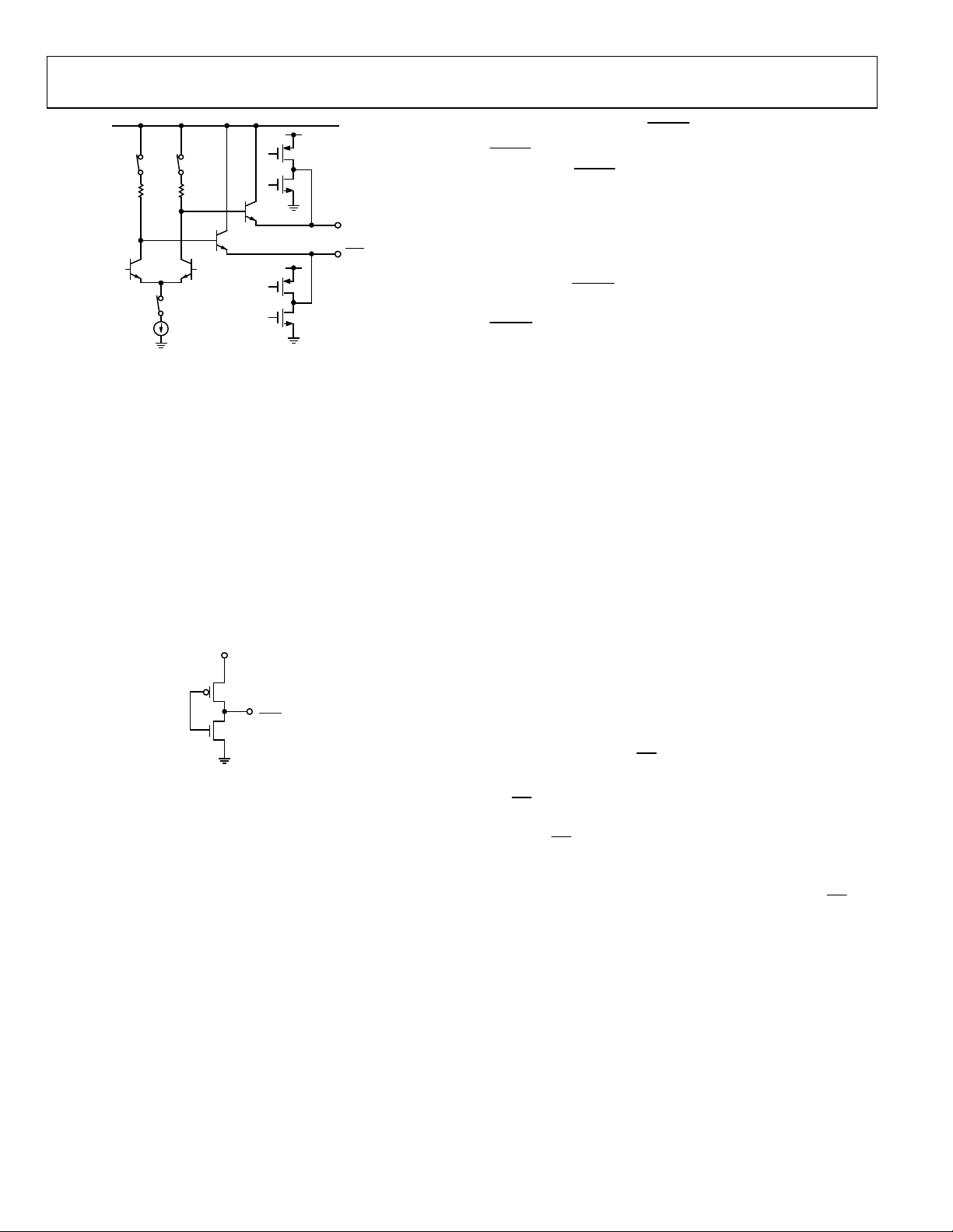
AD9520-5
V
http://www.BDTIC.com/ADI
SW1B SW1A
R2
200ΩR1200Ω
Figure 41. LVPECL Output Simplified Equivalent Circuit
SW2
4.4mA
N1
N2
QN2
QN1
OUT
OUT
07239-058
CMOS Output Drivers
The user can also individually configure each LVPECL output
as a pair of CMOS outputs, which provides up to 24 CMOS
outputs. When an output is configured as CMOS, CMOS
Output A and CMOS Output B are automatically turned on. For
a given differential pair, either CMOS Output A or Output B
can be turned on or off independently. The user can also select
the relative polarity of the CMOS outputs for any combination of
inverting and noninverting (see Register 0x0F0 to Register 0x0FB).
The user can power down each CMOS output as needed to save
power. The CMOS output power-down is individually controlled
by the enable CMOS output register (0x0F0[6:5] to 0x0FB[6:5]).
The CMOS driver is in tristate when it is powered down.
S_DRV
OUT1/
OUT1
07239-035
Figure 42. CMOS Equivalent Output Circuit
RESET MODES
The AD9520 has a power-on reset (POR) and several other
ways to apply a reset condition to the chip.
Power-On Reset
During chip power-up, a power-on reset pulse is issued when
VS reaches ~2.6 V (<2.8 V) and restores the chip either to the
setting stored in EEPROM (with the EEPROM pin = 1) or to
the on-chip setting (with the EEPROM pin = 0). At power-on,
the AD9520 also executes a SYNC operation, which brings the
outputs into phase alignment according to the default settings.
The output drivers are held in sync for the duration of the
internally generated power-up sync timer (~70 ms). The
outputs begin to toggle after this period.
Rev. 0 | Page 44 of 80
Hardware Reset via the
RESET
, a hard reset (an asynchronous hard reset is executed by
briefly pulling
RESET
stored in EEPROM (the EEPROM pin = 1) or to the on-chip
setting (the EEPROM pin = 0). A hard reset also executes a
SYNC operation, which brings the outputs into phase alignment
according to the default settings. When EEPROM is inactive
(the EEPROM pin = 0), it takes ~2 µs for the outputs to begin
toggling after
RESET
EEPROM pin = 1), it takes ~20 ms for the outputs to toggle after
RESET
is brought high.
Soft Reset via the Serial Port
The serial port control register allows for a soft reset by setting
Bit 2 and Bit 5 in Register 0x000. When Bit 5 and Bit 2 are set,
the chip enters a soft reset mode and restores the chip either to
the setting stored in EEPROM (the EEPROM pin = 1) or to the
on-chip setting (the EEPROM pin = 0), except for Register 0x000.
Except for the self-clearing bits, Bit 2 and Bit 5, Register 0x000
retains its previous value prior to reset. During the internal reset,
the outputs hold static. These bits are self-clearing. However, the
self-clearing operation does not complete until an additional
serial port SCLK cycle, and the AD9520 is held in reset until
that happens.
Soft Reset to Settings in EEPROM when EEPROM Pin = 0 via the Serial Port
The serial port control register allows the chip to be reset to
settings in EEPROM when the EEPROM pin = 1 via 0xB02[1].
This bit is self-clearing. This bit does not have any effect when
the EEPROM pin = 0. It takes ~20 ms for the outputs to begin
toggling after the Soft_EEPROM register is cleared.
POWER-DOWN MODES
Chip Power-Down via PD
The AD9520 can be put into a power-down condition by pulling
PD
pin low. Power-down turns off most of the functions and
the
currents inside the AD9520. The chip remains in this power-down
state until
out of power-down mode, the AD9520 returns to the settings
programmed into its registers prior to the power-down, unless
the registers are changed by new programming while the
pin is held low.
Powering down the chip shuts down the currents on the chip,
except for the bias current necessary to maintain the LVPECL
outputs in a safe shutdown mode. The LVPECL bias currents are
needed to protect the LVPECL output circuitry from damage that
can be caused by certain termination and load configurations
when tristated. Because this is not a complete power-down, it
can be called sleep mode. The AD9520 contains special circuitry to
prevent runt pulses on the outputs when the chip is entering or
exiting sleep mode.
PD
is brought back to logic high. When taken
RESET
Pin
low), restores the chip either to the setting
is issued. When EEPROM is active (the
PD

AD9520-5
http://www.BDTIC.com/ADI
When the AD9520 is in a PD power-down, the chip is in the
following state:
• The PLL is off (asynchronous power-down).
• The CLK input buffer is off, but the CLK input dc bias
circuit is on.
• In differential mode, the reference input buffer is off, but
the dc bias circuit is still on.
• In singled-ended mode, the reference input buffer is off,
and the dc bias circuit is off.
• All dividers are off.
• All CMOS outputs are tristated.
• All LVPECL outputs are in safe off mode.
• The serial control port is active, and the chip responds to
commands.
PLL Power-Down
The PLL section of the AD9520 can be selectively powered
down. There are two PLL power-down modes set by
Register 0x010[1:0]: asynchronous and synchronous.
In asynchronous power-down mode, the device powers down as
soon as the registers are updated. In synchronous power-down
mode, the PLL power-down is gated by the charge pump to
prevent unwanted frequency jumps. The device goes into powerdown on the occurrence of the next charge pump event after the
registers are updated.
Distribution Power-Down
The distribution section can be powered down by writing
0x230[1] = 1b, which turns off the bias to the distribution
section. If the LVPECL power-down mode is normal operation
(0b), it is possible for a low impedance load on that LVPECL
output to draw significant current during this power-down. If
the LVPECL power-down mode is set to 1b, the LVPECL output
is not protected from reverse bias and can be damaged under
certain termination conditions.
Individual Clock Output Power-Down
Any of the clock distribution outputs can be powered down
into safe power-down mode by individually writing to the
appropriate registers. The register map details the individual
power-down settings for each output. These settings are found
in Register 0x0F0[0] to Register 0x0FB[0].
Individual Clock Channel Power-Down
Any of the clock distribution channels can be powered down
individually by writing to the appropriate registers. Powering
down a clock channel is similar to powering down an individual
driver, but it saves more power because the dividers are also
powered down. Powering down a clock channel also automatically
powers down the drivers connected to it. The register map
details the individual power-down settings for each output
channel. These settings are found in 0x192[2], 0x195[2],
0x198[2], and 0x19B[2].
Rev. 0 | Page 45 of 80

AD9520-5
A
http://www.BDTIC.com/ADI
SERIAL CONTROL PORT
The AD9520 serial control port is a flexible, synchronous serial
communications port that allows an easy interface with many
industry-standard microcontrollers and microprocessors. The
AD9520 serial control port is compatible with most synchronous
transfer formats, including Philips IC, Motorola® SPI®, and
Intel® SSR protocols. The AD9520 IC implementation deviates
from the classic IC specification on two specifications, and
these deviations are documented in Tabl e 11 of this data sheet.
The serial control port allows read/write access to all registers
that configure the AD9520.
SPI/I²C PORT SELECTION
The AD9520 has two serial interfaces, SPI and IC. Users can
select either SPI or IC depending on the states of the three
logic level (high, open, low) input pins, SP1 and SP0. When
both SP1 and SP0 are high, the SPI interface is active. Otherwise,
IC is active with eight different IC slave address (seven bits
wide) settings, see Tabl e 35. The four MSBs of the slave address
are hardware coded as 1011, and the three LSBs are programmed
by SP1 and SP0.
Table 35. Serial Port Mode Selection
SP1 SP0 Address
Low Low I²C, 1011000
Low Open I²C, 1011001
Low High I²C, 1011010
Open Low I²C, 1011011
Open Open I²C, 1011100
Open High I²C, 1011101
High Low I²C, 1011110
High Open I²C, 1011111
High High SPI
I²C SERIAL PORT OPERATION
The AD9520 IC port is based on the IC fast mode standard.
The AD9520 supports both IC protocols: standard mode
(100 kHz) and fast mode (400 kHz).
The AD9520 IC port has a 2-wire interface consisting of a serial
data line (SDA) and a serial clock line (SCL). In an IC bus system,
the AD9520 is connected to the serial bus (data bus SDA and
clock bus SCL) as a slave device, meaning that no clock is generated
by the AD9520. The AD9520 uses direct 16-bit (two bytes)
memory addressing instead of traditional 8-bit (one byte) memory
addressing.
I2C Bus Characteristics
Table 36. I2C Bus Definitions
Abbreviation Definition
S Start
Sr Repeated start
P
A
A
Stop
Acknowledge
No acknowledge
W Write
R Read
One pulse on the SCL clock line is generated for each data bit
transferred.
The data on the SDA line must not change during the high
period of the clock. The state of the data line can change only when
the clock on the SCL line is low.
SDA
SCL
DATA LINE
STABLE;
DATA VALID
Figure 43. Valid Bit Transfer
CHANGE
OF DATA
ALLOWED
7239-160
A start condition is a transition from high to low on the SDA
line while SCL is high. The start condition is always generated
by the master to initialize the data transfer.
A stop condition is a transition from low to high on the SDA
line while SCL is high. The stop condition is always generated
by the master to end the data transfer.
SD
SCL
S
START
CONDITION
Figure 44. Start and Stop Conditions
P
STOP
CONDITIO N
07239-161
A byte on the SDA line is always eight bits long. An acknowledge
bit must follow every byte. Bytes are sent MSB first.
The acknowledge bit is the ninth bit attached to any 8-bit data
byte. An acknowledge bit is always generated by the receiving
device (receiver) to inform the transmitter that the byte has
been received. It is done by pulling the SDA line low during the
ninth clock pulse after each 8-bit data byte.
Rev. 0 | Page 46 of 80

AD9520-5
SDA
SDA
SDA
http://www.BDTIC.com/ADI
MSB
ACKNOWLEDGE FROM
SLAVE-RECEIV ER
ACKNOWLEDGE FROM
SLAVE-RECEIVER
SCL
S
SCL
S
SCL
S
1 2 8 9 1 2 83 TO 73 TO 7 9 10
Figure 45. Acknowledge Bit
MSB = 0
ACKNOWLEDGE FROM
SLAVE-RECEIV ER
1 2 8 9 1 2 83 TO 73 TO 7 9 10
Figure 46. Data Transfer Process (Master Write Mode, 2-Byte Transfer Used for Illustration)
MSB = 1
ACKNOWLEDGE FROM
MASTER-RECEIVER
1 2 8 9 1 2 83 TO 73 TO 7 9 10
Figure 47. Data Transfer Process (Master Read Mode, 2-Byte Transfer Used for Illustration)
The no acknowledge bit is the ninth bit attached to any 8-bit
data byte. A no acknowledge bit is always generated by the
receiving device (receiver) to inform the transmitter that the
byte has not been received. It is done by leaving the SDA line
high during the ninth clock pulse after each 8-bit data byte.
Data Transfer Process
The master initiates data transfer by asserting a start condition.
This indicates that a data stream follows. All IC slave devices
connected to the serial bus respond to the start condition.
The master then sends an 8-bit address byte over the SDA line,
W
consisting of a 7-bit slave address (MSB first) plus an R/
bit.
This bit determines the direction of the data transfer, that is,
whether data is written to or read from the slave device
(0 = write, 1 = read).
The peripheral whose address corresponds to the transmitted
address responds by sending an acknowledge bit. All other
devices on the bus remain idle while the selected device waits
for data to be read from or written to it. If the R/
W
bit is 0, the
master (transmitter) writes to the slave device (receiver). If the
W
R/
bit is 1, the master (receiver) reads from the slave device
(transmitter).
The format for these commands is described in the Data
Transfe r For mat section.
P
07239-162
ACKNOWLEDGE FROM
SLAVE-RECEI VER
P
07239-163
NO ACKNOWLEDGE
FROM
SLAVE-RECEIV ER
P
07239-164
Data is then sent over the serial bus in the format of nine clock
pulses, one data byte (8-bit) from either master (write mode) or
slave (read mode), followed by an acknowledge bit from the
receiving device. The number of bytes that can be transmitted per
transfer is unrestricted. In write mode, the first two data bytes
immediately after the slave address byte are the internal
memory (control registers) address bytes with the high address
byte first. This addressing scheme gives a memory address up to
16
2
− 1 = 65,535. The data bytes after these two memory address
bytes are register data written into the control registers. In read
mode, the data bytes after the slave address byte are register
data read from the control registers.
When all data bytes are read or written, stop conditions are
established. In write mode, the master (transmitter) asserts a
stop condition to end data transfer during the (10th) clock
pulse following the acknowledge bit for the last data byte from
the slave device (receiver). In read mode, the master device
(receiver) receives the last data byte from the slave device
(transmitter) but does not pull it low during the ninth clock
pulse. This is known as a no acknowledge bit. By receiving the no
acknowledge bit, the slave device knows that the data transfer is
finished and releases the SDA line. The master then takes the
data line low during the low period before the 10th clock pulse
and high during the 10th clock pulse to assert a stop condition.
A repeated start (Sr) condition can be used in place of a stop
condition. Furthermore, a start or stop condition can occur at
any time, and partially transferred bytes are discarded.
Rev. 0 | Page 47 of 80
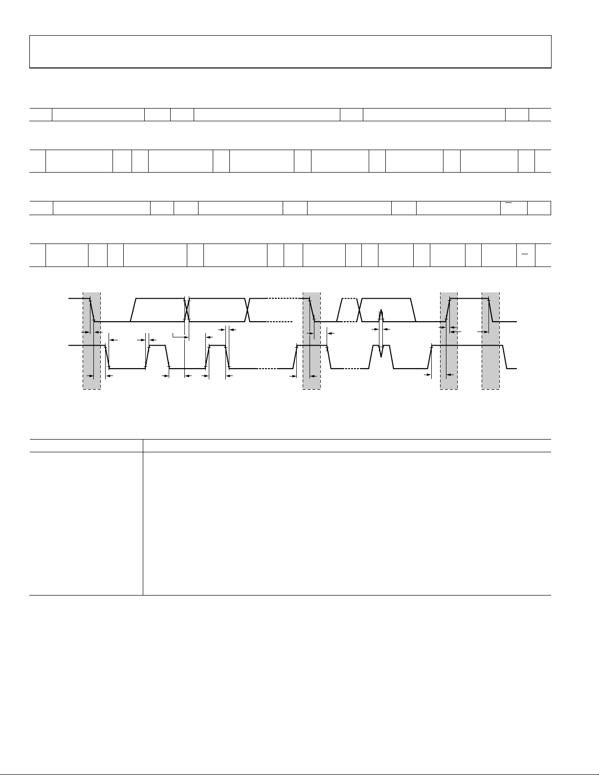
AD9520-5
http://www.BDTIC.com/ADI
Data Transfer Format
Send byte format—the send byte protocol is used to set up the register address for subsequent commands.
S Slave Address W A RAM Address High Byte A RAM Address Low Byte A P
Write byte format—the write byte protocol is used to write a register address to the RAM starting from the specified RAM address.
RAM Address
S Slave Address W A
High Byte A
Receive byte format—the receive byte protocol is used to read the data byte(s) from RAM starting from the current address.
S Slave Address R A RAM Data 0 A RAM Data 1 A RAM Data 2
Read byte format—the combined format of the send byte and the receive byte.
Slave
S
Address W A
RAM Address
High Byte A
I²C Serial Port Timing
SDA
t
SET; DAT
t
RISE
SCL
t
FALL
t
LOW
RAM Address
Low Byte A RAM Data 0 A RAM Data 1 A RAM Data 2 A P
RAM Address
Low Byte A Sr
t
FALL
Slave
Address R A
t
HLD; STR
RAM
Data 0 A
t
SPIKE
RAM
Data 1 A
t
RISE
t
IDLE
RAM
Data 2
A
P
A
P
t
HLD; STR
S Sr P S
t
HLD; DAT
t
HIGH
t
SET; STR
Figure 48. I²C Serial Port Timing
Table 37. IC Timing Definitions
Parameter Description
f
I²C clock frequency
I2C
t
Bus idle time between stop and start conditions
IDLE
t
Hold time for repeated start condition
HLD; STR
t
Setup time for repeated start condition
SET; STR
t
Setup time for stop condition
SET; STP
t
Hold time for data
HLD; DAT
t
Setup time for data
SET; DAT
t
Duration of SCL clock low
LOW
t
Duration of SCL clock high
HIGH
t
SCL/SDA rise time
RISE
t
SCL/SDA fall time
FAL L
t
Voltage spike pulse width that must be suppressed by the input filter
SPIKE
t
SET; STP
07239-165
Rev. 0 | Page 48 of 80

AD9520-5
http://www.BDTIC.com/ADI
SPI SERIAL PORT OPERATION
Pin Descriptions
SCLK (serial clock) is the serial shift clock. This pin is an input.
SCLK is used to synchronize serial control port reads and writes.
Write data bits are registered on the rising edge of this clock,
and read data bits are registered on the falling edge. This pin is
internally pulled down by a 30 kΩ resistor to ground.
SDIO (serial data input/output) is a dual-purpose pin and acts
either as an input only (unidirectional mode) or as an input/
output (bidirectional mode). The AD9520 defaults to the
bidirectional I/O mode (0x000[7] = 0b).
SDO (serial data out) is used only in the unidirectional I/O
mode (0x000[7]) as a separate output pin for reading back data.
CS
(chip select bar) is an active low control that gates the read
and write cycles. When
impedance state. This pin is internally pulled up by a 30 kΩ
resistor to VS.
SPI Mode Operation
In SPI mode, single or multiple byte transfers are supported, as
well as MSB first or LSB first transfer formats. The AD9520
serial control port can be configured for a single bidirectional
I/O pin (SDIO only) or for two unidirectional I/O pins (SDIO/
SDO). By default, the AD9520 is in bidirectional mode. Short
instruction mode (8-bit instruction) is not supported. Only
long (16-bit) instruction mode is supported.
A write or a read operation to the AD9520 is initiated by pulling
CS
low.
CS
The
stalled high mode is supported in data transfers where
three or fewer bytes of data (plus instruction data) are transferred
(see ). In this mode, the Tab l e 3 8
high on any byte boundary, allowing time for the system controller
to process the next byte.
and can go high during either part (instruction or data) of the
transfer.
During this period, the serial control port state machine enters
a wait state until all data is sent. If the system controller decides
to abort the transfer before all of the data is sent, the state machine
must be reset by either completing the remaining transfers or by
returning
CS
low for at least one complete SCLK cycle (but
fewer than eight SCLK cycles). Raising the
boundary terminates the serial transfer and flushes the buffer.
CS
is high, SDO and SDIO are in a high
15
CS
SCLK/SCL
SDIO/SDA
SDO
Figure 49. Serial Control Port
CS
AD9520
16
SERIAL
17
CONTROL
PORT
18
CS
pin can temporarily return
can go high on byte boundaries only
CS
07239-036
pin on a nonbyte
In the streaming mode (see Tab l e 38), any number of data bytes
can be transferred in a continuous stream. The register address
is automatically incremented or decremented (see the SPI
MSB/LSB First Transfers section).
CS
must be raised at the end
of the last byte to be transferred, thereby ending streaming mode.
Communication Cycle—Instruction Plus Data
There are two parts to a communication cycle with the AD9520.
The first part writes a 16-bit instruction word into the AD9520,
coincident with the first 16 SCLK rising edges. The instruction
word provides the AD9520 serial control port with information
regarding the data transfer, which is the second part of the
communication cycle. The instruction word defines whether
the upcoming data transfer is a read or a write, the number of
bytes in the data transfer, and the starting register address for
the first byte of the data transfer.
Write
If the instruction word is for a write operation, the second part
is the transfer of data into the serial control port buffer of the
AD9520. Data bits are registered on the rising edge of SCLK.
The length of the transfer (one, two, or three bytes or streaming
mode) is indicated by two bits (W1:W0) in the instruction byte.
When the transfer is one, two, or three bytes, but not streaming,
CS
can be raised after each sequence of eight bits to stall the bus
(except after the last byte, where it ends the cycle). When the bus
is stalled, the serial transfer resumes when
CS
the
pin on a nonbyte boundary resets the serial control port.
CS
is lowered. Raising
During a write, streaming mode does not skip over reserved or
blank registers, and the user can write 0x00 to the reserved
register addresses.
Because data is written into a serial control port buffer area, not
directly into the actual control registers of the AD9520, an
additional operation is needed to transfer the serial control port
buffer contents to the actual control registers of the AD9520,
thereby causing them to become active. The update registers
operation consists of setting 0x232[0] = 1b (this bit is selfclearing). Any number of bytes of data can be changed before
executing an update registers. The update registers simultaneously
actuates all register changes that have been written to the buffer
since any previous update.
Read
The AD9520 supports only the long instruction mode. If the
instruction word is for a read operation, the next N × 8 SCLK
cycles clock out the data from the address specified in the
instruction word, where N is 1 to 3 as determined by W1:W0.
If N = 4, the read operation is in streaming mode, continuing
CS
until
is raised. Streaming mode does not skip over reserved
or blank registers. The readback data is valid on the falling
edge of SCLK.
Rev. 0 | Page 49 of 80
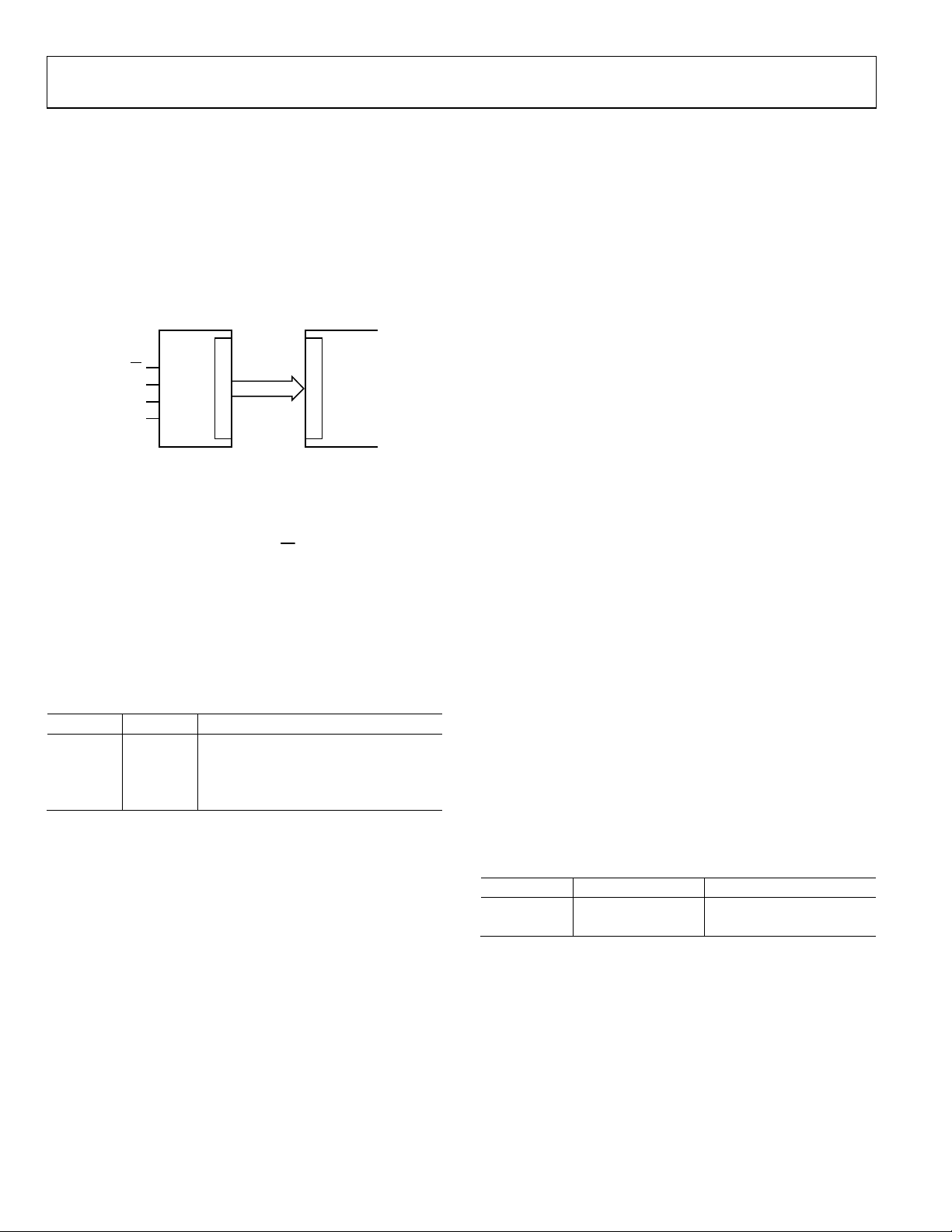
AD9520-5
http://www.BDTIC.com/ADI
The default mode of the AD9520 serial control port is the
bidirectional mode. In bidirectional mode, both the sent data
and the readback data appear on the SDIO pin. It is also possible to
set the AD9520 to unidirectional mode (0x000[7] = 1 and
0x000[0] = 1). In unidirectional mode, the readback data
appears on the SDO pin.
A readback request reads the data that is in the serial control port
buffer area or the data that is in the active registers (see Figure 50).
Readback of the buffer or active registers is controlled by 0x004[0].
The AD9520 uses Register Address 0x000 to Register Address 0xB03.
CS
SCLK/SCL
SDIO/SDA
SERIAL
SDO
CONTROL
PORT
WRITE REGISTER 0x232 = 0x001
TO UPDATE REG ISTERS
Figure 50. Relationship Between Serial Control Port Buffer Registers and
Active Registers of the AD9520
UPDATE
REGISTERS
BUFFER REGIS TERS
ACTIVE REGISTERS
07239-037
SPI INSTRUCTION WORD (16 BITS)
The MSB of the instruction word is R/W, which indicates
whether the instruction is a read or a write. The next two bits
(W1:W0) indicate the length of the transfer in bytes. The final
13 bits are the address (A12:A0) at which to begin the read or
write operation.
For a write, the instruction word is followed by the number of
bytes of data indicated by Bits[W1:W0], see Tab l e 38 .
Table 38. Byte Transfer Count
W1
0 0 1
0 1 2
1 0 3
1
Bits[A12:A0] select the address within the register map that is
written to or read from during the data transfer portion of the
communications cycle. Only Bits[A9:A0] are needed to cover
the range of the 0x232 registers used by the AD9520. Bits[A12:A10]
must always be 0b. For multibyte transfers, this address is the
starting byte address. In MSB first mode, subsequent bytes
increment the address.
W0 Bytes to Transfer
1 Streaming mode
SPI MSB/LSB FIRST TRANSFERS
The AD9520 instruction word and byte data can be MSB first
or LSB first. Any data written to 0x000 must be mirrored; the
upper four bits ([7:4]) must mirror the lower four bits ([3:0]).
This makes it irrelevant whether LSB first or MSB first is in
effect. As an example of this mirroring, see the default setting
for 0x000, which mirrors Bit 4 and Bit 3. This sets the long
instruction mode, which is the default and the only mode
supported.
The default for the AD9520 is MSB first.
When LSB first is set by 0x000[1] and 0x000[6], it takes effect
immediately because it only affects the operation of the serial
control port and does not require that an update be executed.
When MSB first mode is active, the instruction and data bytes
must be written from MSB to LSB. Multibyte data transfers in
MSB first format start with an instruction byte that includes the
register address of the most significant data byte. Subsequent
data bytes must follow in order from the high address to the
low address. In MSB first mode, the serial control port internal
address generator decrements for each data byte of the multibyte
transfer cycle.
When LSB first is active, the instruction and data bytes must be
written from LSB to MSB. Multibyte data transfers in LSB first
format start with an instruction byte that includes the register
address of the least significant data byte followed by multiple
data bytes. In a multibyte transfer cycle, the internal byte
address generator of the serial port increments for each byte.
The AD9520 serial control port register address decrements
from the register address just written toward 0x000 for multibyte
I/O operations if the MSB first mode is active (default). If the
LSB first mode is active, the register address of the serial control
port increments from the address just written toward 0x232 for
multibyte I/O operations.
Streaming mode always terminates when it reaches 0x232. Note
that unused addresses are not skipped during multibyte I/O
operations.
Table 39. Streaming Mode (No Addresses Are Skipped)
Write Mode
LSB first Increment 0x230, 0x231, 0x232, stop
MSB first Decrement 0x001, 0x000, 0x232, stop
Address Direction Stop Sequence
Rev. 0 | Page 50 of 80
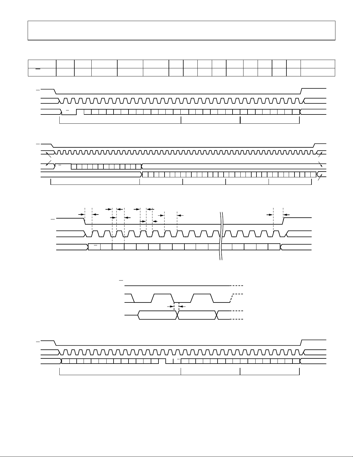
AD9520-5
http://www.BDTIC.com/ADI
Table 40. Serial Control Port, 16-Bit Instruction Word, MSB First
MSB LSB
I15 I14 I13 I12 I11 I10 I9 I8 I7 I6 I5 I4 I3 I2 I1 I0
R/W
SCLK
CS
DON'T CARE
W1 W0 A12 = 0 A11 = 0 A10 = 0 A9 A8 A7 A6 A5 A4 A3 A2 A1 A0
DON'T CARE
DON'T CARE
SDIO A12W0W1R/W A11 A10 A9 A8 A7 A6 A5 A4 A3 A2 A1 A0 D7 D6 D5 D4 D3 D2 D1 D0 D7 D6 D5 D4 D3 D2 D1 D0
16-BIT INST RUCTION HEADE R REGISTE R (N) DATA REG ISTER (N – 1) DAT A
Figure 51. Serial Control Port Write—MSB First, 16-Bit Instruction, Two Bytes of Data
CS
SCLK
DON'T CARE
SDIO
SDO
DON'T CARE
A12W0W1R/W A11 A10 A9 A8 A7 A6 A5 A4 A3 A2 A1 A0
D7 D6 D5 D4 D3 D2 D1 D0 D7 D6 D5 D4 D3 D2 D1 D0 D7 D6 D5 D4 D3 D2 D1 D0 D7 D6 D5 D4 D3 D2 D1 D0
REGISTE R (N) DATA16-BIT INST RUCTION HE ADER REGISTER (N – 1) DATA REGI STER (N – 2) DATA REG ISTER (N – 3) DAT A
Figure 52. Serial Control Port Read—MSB First, 16-Bit Instruction, Four Bytes of Data
t
HIGH
t
CLK
t
C
DON'T CARE
DON'T CARE
SCLK
SDIO
CS
DON'T CARE
DON'T CARE
t
DS
t
S
R/W
t
DH
t
LOW
W1W0A12A11A10A9A8A7A6A5D4D3D2D1D0
Figure 53. Serial Control Port Write—MSB First, 16-Bit Instruction, Timing Measurements
CS
DON'T CARE
DON'T CARE
DON'T
CARE
07239-040
7239-038
07239-039
SCLK
SDIO
SDO
CS
DON'T CARE
SCLK
SDIO
DON'T CARE
A0 A1 A2 A3 A4 A5 A6 A7 A8 A9 A1 0 A11 A12 D1D0R/ WW1W0 D2 D3 D4 D5 D6 D7 D0 D1 D2 D3 D4 D5 D6 D7
16-BIT INST RUCTION HEADE R REGISTE R (N) DATA REGI STER (N + 1) DAT A
Figure 55. Serial Control Port Write—LSB First, 16-Bit Instruction, Two Bytes of Data
t
DV
DATA BIT N – 1DATA BIT N
Figure 54. Timing Diagram for Serial Control Port Register Read
Rev. 0 | Page 51 of 80
07239-041
DON'T CARE
DON'T CARE
7239-042

AD9520-5
http://www.BDTIC.com/ADI
t
S
CS
t
CLK
SCLK
SDIO
t
HIGH
t
DS
t
DH
BIT N BIT N + 1
t
LOW
Figure 56. Serial Control Port Timing—Write
Table 41. Serial Control Port Timing
Parameter Description
tDS Setup time between data and rising edge of SCLK
tDH Hold time between data and rising edge of SCLK
t
Period of the clock
CLK
tS
tC
t
Minimum period that SCLK should be in a logic high state
HIGH
t
Minimum period that SCLK should be in a logic low state
LOW
t
SCLK to valid SDIO and SDO (see Figure 54)
DV
Setup time between the CS falling edge and SCLK rising edge (start of communication cycle)
Setup time between SCLK rising edge and the CS
t
C
rising edge (end of communication cycle)
7239-043
Rev. 0 | Page 52 of 80

AD9520-5
http://www.BDTIC.com/ADI
EEPROM OPERATIONS
The AD9520 contains an internal EEPROM (nonvolatile memory).
The EEPROM can be programmed by users to create and store
a user-defined register setting file when the power is off. This
setting file can be used for power-up and chip reset as a default
setting. The EEPROM size is 512 bytes.
During the data transfer process, the write and read registers via
the serial port are generally not available except for one readback
register, STATUS_EEPROM.
To determine the data transfer state through the serial port in
SPI mode, users can read the value of STATUS_EEPROM (1 =
in process and 0 = completed).
In IC mode, the user can address the AD9520 slave port with
the external IC master (send an address byte to the AD9520). If
the AD9520 responds with a no acknowledge bit, the data transfer
process is not done. If the AD9520 responds with an acknowledge
bit, the data transfer process is completed. The user can monitor
the STATUS_EEPROM register or program the STATUS pin to
monitor the status of the data transfer.
WRITING TO THE EEPROM
The EEPROM cannot be programmed directly through the serial
port interface. To program the EEPROM and store a register
setting file, do the following:
1. Program the AD9520 registers to the desired circuit state.
2. Program the EEPROM buffer registers, if necessary (see
the Programming the EEPROM Buffer Segment section).
This is only necessary if users want to use the EEPROM to
control the default setting of some (but not all) of the
AD9520 registers, or if they want to control the register
setting update sequence during power-up or chip reset.
3. Set the enable EEPROM write bit (0xB02[0]) to 1 to enable
the EEPROM.
4. Set the REG2EEPROM bit (0xB03[0]) to 1.
5. Set the IO_UPDATE bit (0x232[0]) to 1, which starts the
process of writing data into the EEPROM to create the
EEPROM setting file. This enables the AD9520 EEPROM
controller to transfer the current register values, as well as
the memory address and instruction bytes from the EEPROM
buffer segment, into the EEPROM. After the write process
is completed, the internal controller sets 0xB03[0]
(REG2EEPROM) back to 0.
The readback register STATUS_EEPROM (0xB00[0]) is
used to indicate the data transfer status between the
EEPROM and the control registers (0 = done/inactive;
1 = in process/ active). At the beginning of the data
transfer, STATUS_EEPROM is set to 1 by the EEPROM
controller and cleared to 0 at the end of the data transfer.
The user can access STATUS_EEPROM through the
STATUS pin when the STATUS pin is programmed to
monitor STATUS_EEPROM. Alternatively, the user can
monitor the STATUS_EEPROM bit.
6. After the data transfer process is done (0xB00[0] = 0), set
the enable EEPROM write register (0xB02[0]) to 0 to
disable writing to the EEPROM.
To verify that the data transfer has completed correctly, the user
can verify that 0xB01[0] = 0. A value of 1 in this register indicates a
data transfer error.
READING FROM THE EEPROM
The following reset-related events can start the process of
restoring the settings stored in EEPROM to control registers.
When the EEPROM pin is set high, do any of the following:
1. Power-up the AD9520.
2. Perform a hardware chip reset by pulling the
low, and then releasing
3. Set the self-clearing soft reset bit (0x000[5]) to 1.
When the EEPROM pin is set low, set the self-clearing
Soft_EEPROM bit (0xB02[1]) to 1. The AD9520 then starts to
read the EEPROM and loads the values into the AD9520.
If the EEPROM pin is low during reset or power-up, the
EEPROM is not active, and the AD9520 default values are
loaded instead.
To verify that the data transfer has completed correctly, the user
can verify that 0xB01[0] = 0. A value of 1 in this register indicates a
data transfer error.
RESET
.
RESET
pin
PROGRAMMING THE EEPROM BUFFER SEGMENT
The EEPROM buffer segment is a register space on the AD9520
that allows the user to specify which groups of registers are
stored to the EEPROM during EEPROM programming. Normally,
this segment does not need to be programmed by the user. Instead,
the default power-up values for the EEPROM buffer segment
allow the user to store all of the AD9520 register values from
Register 0x000 to Register 0x231 to the EEPROM.
For example, if users want to load only the output driver settings
from the EEPROM without disturbing the PLL register settings
currently stored in the AD9520, they can alter the EEPROM buffer
segment to include only the registers that apply to the output
drivers and exclude the registers that apply to the PLL
configuration.
There are two parts to the EEPROM buffer segment: register
section definition groups and operational codes. Each register
section definition group contains the starting address and
number of bytes to be written to the EEPROM.
Rev. 0 | Page 53 of 80

AD9520-5
http://www.BDTIC.com/ADI
If the AD9520 register map were continuous from Address 0x000
to Address 0x232, only one register section definition group
would consist of a starting address of 0x000 and a length of
563 bytes. However, this is not the case. The AD9520 register
map is noncontiguous, and the EEPROM is only 512 bytes long.
Therefore, the register section definition group tells the EEPROM
controller how the AD9520 register map is segmented.
There are three operational codes: IO_UPDATE, end-of-data,
and pseudo-end-of-data. It is important that the EEPROM buffer
segment always have either an end-of-data or a pseudo-end-of-data
operational code and that an IO_UPDATE operation code appear
at least once before the end-of-data op code.
Register Section Definition Group
The register section definition group is used to define a continuous
register section for the EEPROM profile. It consists of three bytes.
The first byte defines how many continuous register bytes are in
this group. If the user puts 0x000 in the first byte, it means there
is only one byte in this group. If the user puts 0x001, it means
there are two bytes in this group. The maximum number of
registers in one group is 128.
The next two bytes are the low byte and high byte of the
memory address (16-bit) of the first register in this group.
IO_UPDATE (Operational Code 0x80)
The EEPROM controller uses this operational code to generate
an IO_UPDATE signal to update the active control register
bank from the buffer register bank during the download process.
At a minimum, there should be at least one IO_UPDATE
operational code after the end of the final register section definition
group. This is needed is so that at least one IO_UPDATE occurs
after all of the AD9520 registers are loaded when the EEPROM
is read. If this operational code is absent during a write to the
EEPROM, the register values loaded from the EEPROM are not
transferred to the active register space, and these values do not
take effect after they are loaded from the EEPROM to the AD9520.
End-of-Data (Operational Code 0xFF)
The EEPROM controller uses this operational code to terminate
the data transfer process between EEPROM and the control
register during the upload and download process. The last item
appearing in the EEPROM buffer segment should be either this
operational code or the pseudo-end-of-data operational code.
Pseudo-End-of-Data (Operational Code 0xFE)
The AD9520 EEPROM buffer segment has 23 bytes that can
contain up to seven register section definition groups. If users
want to define more than seven register section definition
groups, the pseudo-end-of-data operational code can be used.
During the upload process, when the EEPROM controller
receives the pseudo-end-of-data operational code, it halts the
data transfer process, clears the REG2EEPROM bit, and enables
the AD9520 serial port. Users can then program the EEPROM
buffer segment again and reinitiate the data transfer process by
setting the REG2EEPROM bit (0xB03) to 1 and the IO_UPDATE
register (0x232) to 1. The internal IC master then begins writing to
the EEPROM starting from the EEPROM address held from the
last writing.
This sequence enables more discrete instructions to be written
to the EEPROM than would otherwise be possible due to the
limited size of the EEPROM buffer segment. It also permits the
user to write to the same register multiple times with a different
value each time.
Table 42. Example of EEPROM Buffer Segment
Reg Addr (Hex) Bit 7 (MSB) Bit 6 Bit 5 Bit 4 Bit 3 Bit 2 Bit 1 Bit 0 (LSB)
Start EEPROM Buffer Segment
0xA00 0 Number of bytes [6:0] of the first group of registers
0xA01 Address [15:8] of the first group of registers
0xA02 Address [7:0] of the first group of registers
0xA03 0 Number of bytes [6:0] of the second group of registers
0xA04 Address [15:8] of the second group of registers
0xA05 Address [7:0] of the second group of registers
0xA06 0 Number of bytes [6:0] of the third group of registers
0xA07 Address [15:8] of the third group of registers
0xA08 Address [7:0] of the third group of registers
0xA09 IO_UPDATE operational code (0x80)
0xA0A End-of-data operational code (0xFF)
Rev. 0 | Page 54 of 80

AD9520-5
http://www.BDTIC.com/ADI
THERMAL PERFORMANCE
Table 43. Thermal Parameters for 64-Lead LFCSP
Symbol Thermal Characteristic Using a JEDEC JESD51-7 Plus JEDEC JESD51-5 2S2P Test Board Value (°C/W)
θJA Junction-to-ambient thermal resistance, 0.0 m/sec airflow per JEDEC JESD51-2 (still air) 22.0
θ
Junction-to-ambient thermal resistance, 1.0 m/sec airflow per JEDEC JESD51-6 (moving air) 19.2
JMA
θ
Junction-to-ambient thermal resistance, 2.0 m/sec airflow per JEDEC JESD51-6 (moving air) 17.2
JMA
ΨJB
Junction-to-board characterization parameter, 1.0 m/sec airflow per JEDEC JESD51-6 (moving air)
and JEDEC JESD51-8
θJC Junction-to-case thermal resistance (die-to-heat sink) per MIL-Std 883, Method 1012.1 1.3
ΨJT Junction-to-top-of-package characterization parameter, 0 m/sec airflow per JEDEC JESD51-2 (still air) 0.1
The AD9520 is specified for a case temperature (T
that T
is not exceeded, an airflow source can be used.
CASE
). To ensure
CASE
Use the following equation to determine the junction
temperature on the application PCB:
= T
T
J
+ (ΨJT × PD)
CASE
where:
T
is the junction temperature (°C).
J
T
is the case temperature (°C) measured by the user at the
CASE
top center of the package.
Ψ
is the value from Tabl e 43.
JT
PD is the power dissipation (see the total power dissipation in
Valu es o f θ
design considerations. θ
approximation of T
where T
Valu es o f θ
are provided for package comparison and PCB
JA
can be used for a first-order
JA
by the equation
J
= TA + (θJA × PD)
T
J
is the ambient temperature (°C).
A
are provided for package comparison and PCB
JC
design considerations when an external heat sink is required.
Valu es o f Ψ
are provided for package comparison and PCB
JB
design considerations.
Tabl e 15 .)
11.6
Rev. 0 | Page 55 of 80

AD9520-5
http://www.BDTIC.com/ADI
REGISTER MAP
Register addresses that are not listed in Tab l e 44 are not used, and writing to those registers has no effect. The user should avoid writing
values other than 00h to register addresses marked unused.
Table 44. Register Map Overview
Default
Addr
(Hex) Parameter Bit 7 (MSB) Bit 6 Bit 5 Bit 4 Bit 3 Bit 2 Bit 1 Bit 0 (LSB)
Serial Port Configuration
000 Serial port
config
(SPI mode)
Serial port
config
(I²C mode)
001 Unused N/A
002 Reserved (read-only) N/A
003 Reserved (read-only) N/A
004 Readback
control
EEPROM ID
005 EEPROM
customer
006 EEPROM customer version ID (MSB) 00
version ID
007
Unused 00
to
00F
PLL
010 PFD charge
pump
011
R counter
012 Unused 14-bit R counter, Bits[13:8] (MSB) 00
013 A counter Unused 6-bit A counter 00
014
B counter
015 Unused 13-bit B counter, Bits[12:8] (MSB) 00
016 PLL_CTRL_1 Set CP pin
017 PLL_CTRL_2 STATUS pin control Antibacklash pulse width 00
018 PLL_CTRL_3 Enable CMOS
019 PLL_CTRL_4 R, A, B counters
01A PLL_CTRL_5 Enable
01B PLL_CTRL_6 Enable CLK
01C PLL_CTRL_7 Disable
01D PLL_CTRL_8 Enable
SDO active LSB first/
PFD polarity Charge pump current Charge pump mode PLL power-down 7D
to VCP/2
reference
input
dc offset
SYNC
STATUS
pin divider
frequency
monitor
switchover
deglitch
Status_EEPROM
at STATUS pin
addr incr
Unused Soft reset
Reset
R counter
pin reset
Ref freq
monitor
threshold
Enable
REF2
REFIN
(
frequency
monitor
Select
REF2
Enable
XTAL
OSC
Soft reset
(selfclearing)
(selfclearing)
Reset
A and B
counters
Lock detect
counter
Enable
REF1
(REFIN)
)
frequency
monitor
Use
REF_SEL
pin
Enable
clock
doubler
Unused Unused Soft reset
Unused Unused Soft reset
Unused Readback
EEPROM customer version ID (LSB) 00
14-bit R counter, Bits[7:0] (LSB) 01
13-bit B counter, Bits[7:0] (LSB) 03
Reset all
counters
Digital
lock
detect
window
R path delay N path delay 00
Enable
automatic
reference
switchover
Disable
PLL status
register
B counter
bypass
Disable
digital
lock
detect
Stay on REF2 Enable
Enable
LD pin
comparator
(selfclearing)
(selfclearing)
LD pin control 00
REFMON pin control 00
REF2
Unused Enable
LSB first/
addr incr
Prescaler P 06
Unused 06
Enable
REF1
external
holdover
SDO active 00
Unused 00
active regs
Enable
differential
reference
Enable
holdover
Value
(Hex)
00
00
80
Rev. 0 | Page 56 of 80

AD9520-5
http://www.BDTIC.com/ADI
Default
Addr
(Hex) Parameter Bit 7 (MSB) Bit 6 Bit 5 Bit 4 Bit 3 Bit 2 Bit 1 Bit 0 (LSB)
01E PLL_CTRL_9 Unused Enable
01F PLL_Readback
(read-only)
Output Driver Control
0F0 OUT0 control OUT0 format OUT0 CMOS
0F1 OUT1 control OUT1 format OUT1 CMOS
0F2 OUT2 control OUT2 format OUT2 CMOS
0F3 OUT3 control OUT3 format OUT3 CMOS
0F4 OUT4 control OUT4 format OUT4 CMOS
0F5 OUT5 control OUT5 format OUT5 CMOS
0F6 OUT6 control OUT6 format OUT6 CMOS
0F7 OUT7 control OUT7 format OUT7 CMOS
0F8 OUT8 control OUT8 format OUT8 CMOS
0F9 OUT9 control OUT9 format OUT9 CMOS
0FA OUT10 control OUT10 format OUT10 CMOS
0FB OUT11 control OUT11 format OUT11 CMOS
0FC Enable output
on CSDLD
0FD Enable output
on CSDLD
0FE
Unused 00
to
18F
LVPECL Channel Dividers
190 Divider 0
(PECL)
191 Divider 0
192 Unused Channel 0
CSDLD En
OUT7
bypass
Unused Holdover
CSDLD En
OUT6
Divider 0 low cycles Divider 0 high cycles 77
Divider 0
ignore
SYNC
active
configuration
configuration
configuration
configuration
configuration
configuration
configuration
configuration
configuration
configuration
configuration
configuration
CSDLD En
OUT5
Unused CSDLD En
Divider 0
force
high
REF2
selected
CSDLD En
OUT4
Divider 0
start
high
CLK
freq >
threshold
OUT0 polarity OUT0 LVPECL
OUT1 polarity OUT1 LVPECL
OUT2 polarity OUT2 LVPECL
OUT3 polarity OUT3 LVPECL
OUT4 polarity OUT4 LVPECL
OUT5 polarity OUT5 LVPECL
OUT6 polarity OUT6 LVPECL
OUT7 polarity OUT7 LVPECL
OUT8 polarity OUT8 LVPECL
OUT9 polarity OUT9 LVPECL
OUT10 polarity OUT10 LVPECL
OUT11 polarity OUT11 LVPECL
CSDLD En
OUT3
OUT11
REF2
freq >
threshold
CSDLD
En OUT2
CSDLD
En OUT10
power-
down
zero delay
REF1 freq >
threshold
differential voltage
differential voltage
differential voltage
differential voltage
differential voltage
differential voltage
differential voltage
differential voltage
differential voltage
differential voltage
differential voltage
differential voltage
CSDLD En
OUT1
CSDLD En
OUT9
Divider 0
phase offset
Channel 0
direct-to-
output
Unused 00
Digital lock
detect
OUT0
LVPECL
power-down
OUT1
LVPECL
power-down
OUT2
LVPECL
power-down
OUT3
LVPECL
power-down
OUT4
LVPECL
power-down
OUT5
LVPECL
power-down
OUT6
LVPECL
power-down
OUT7
LVPECL
power-down
OUT8
LVPECL
power-down
OUT9
LVPECL
power-down
OUT10
LVPECL
power-down
OUT11
LVPECL
power-down
CSDLD En
OUT0
CSDLD En
OUT8
Disable
Divider 0
DCC
Value
(Hex)
N/A
64
64
64
64
64
64
64
64
64
64
64
64
00
00
00
00
Rev. 0 | Page 57 of 80

AD9520-5
http://www.BDTIC.com/ADI
Default
Addr
(Hex) Parameter Bit 7 (MSB) Bit 6 Bit 5 Bit 4 Bit 3 Bit 2 Bit 1 Bit 0 (LSB)
193 Divider 1
(PECL)
194 Divider 1
195 Unused Unused Channel 1
196 Divider 2
(PECL)
197 Divider 2
198 Unused Unused Channel 2
199 Divider 3
(PECL)
19A Divider 3
19B Unused Unused Channel 3
Unused 00
19C
to
1DF
VCO Divider and CLK Input
1E0 VCO divider Unused Unused VCO divider 00
1E1 Input CLKs Unused Unused
1E2
Unused 00
to
22A
System
230 Power-down
and SYNC
231 Unused Unused 00
Update All Registers
232 IO_UPDATE Unused IO_UPDATE
Unused 00
233
to
9FF
EEPROM Buffer Segment
A00 EEPROM
Buffer
Segment
Register 1
A01 EEPROM
Buffer
Segment
Register 2
A02 EEPROM
Buffer
Segment
Register 3
A03 EEPROM
Buffer
Segment
Register 4
bypass
bypass
bypass
0 EEPROM Buffer Segment Register 1 (default: number of bytes for Group 1) 00
0 EEPROM Buffer Segment Register 4 (default: number of bytes for Group 2) 02
Divider 1 low cycles Divider 1 high cycles 33
Divider 1
ignore
SYNC
Divider 2 low cycles Divider 2 high cycles 11
Divider 2
ignore
SYNC
Divider 3 low cycles Divider 3 high cycles 00
Divider 3
ignore
SYNC
EEPROM Buffer Segment Register 2 (default: Bits[15:8] of starting register address for Group 1) 00
EEPROM Buffer Segment Register 3 (default: Bits[7:0] of starting register address for Group 1) 00
Divider 1
force
high
Divider 2
force
high
Divider 3
force
high
(default = 01b)
Unused Disable
Divider 1
start high
Divider 2
start high
Divider 3
start high
Power down
clock
input
section
power-on
SYNC
Rev. 0 | Page 58 of 80
Divider 1
phase offset
power-
down
Divider 2
phase offset
power-
down
Divider 3
phase offset
Channel 3
powerdown
Reserved Bypass
Powerdown
SYNC
direct-to-
output
Power-
down
distribution
reference
Channel 1
direct-to-
output
Channel 2
direct-to-
output
Disable
Divider 1
DCC
Disable
Divider 2
DCC
Disable
Divider 3
DCC
VCO
divider
Soft
SYNC
(self-clearing)
Value
(Hex)
00
00
00
00
00
00
20
00
00

AD9520-5
http://www.BDTIC.com/ADI
Default
Addr
(Hex) Parameter Bit 7 (MSB) Bit 6 Bit 5 Bit 4 Bit 3 Bit 2 Bit 1 Bit 0 (LSB)
A04 EEPROM
Buffer
Segment
Register 5
A05 EEPROM
Buffer
Segment
Register 6
A06 EEPROM
Buffer
Segment
Register 7
A07 EEPROM
Buffer
Segment
Register 8
A08 EEPROM
Buffer
Segment
Register 9
A09 EEPROM
Buffer
Segment
Register 10
A0A EEPROM
Buffer
Segment
Register 11
A0B EEPROM
Buffer
Segment
Register 12
A0C EEPROM
Buffer
Segment
Register 13
A0D EEPROM
Buffer
Segment
Register 14
A0E EEPROM
Buffer
Segment
Register 15
A0F EEPROM
Buffer
Segment
Register 16
A10 EEPROM
Buffer
Segment
Register 17
A11 EEPROM
Buffer
Segment
Register 18
A12 EEPROM
Buffer
Segment
Register 19
A13 EEPROM
Buffer
Segment
Register 20
EEPROM Buffer Segment Register 5 (default: Bits[15:8] of starting register address for Group 2) 00
EEPROM Buffer Segment Register 6 (default: Bits[7:0] of starting register address for Group 2) 04
0 EEPROM Buffer Segment Register 7 (default: number of bytes for Group 3) 0E
EEPROM Buffer Segment Register 8 (default: Bits[15:8] of starting register address for Group 3) 00
EEPROM Buffer Segment Register 9 (default: Bits[7:0] of starting register address for Group 3) 10
0 EEPROM Buffer Segment Register 10 (default: number of bytes for Group 4) 0E
EEPROM Buffer Segment Register 11 (default: Bits[15:8] of starting register address for Group 4) 00
EEPROM Buffer Segment Register 12 (default: Bits[7:0] of starting register address for Group 4) F0
0 EEPROM Buffer Segment Register 13 (default: number of bytes for Group 5) 0B
EEPROM Buffer Segment Register 14 (default: Bits[15:8] of starting register address for Group 5) 01
EEPROM Buffer Segment Register 15 (default: Bits[7:0] of starting register address for Group 5) 90
0 EEPROM Buffer Segment Register 16 (default: number of bytes for Group 6) 01
EEPROM Buffer Segment Register 17 (default: Bits[15:8] of starting register address for Group 6) 01
EEPROM Buffer Segment Register 18 (default: Bits[7:0] of starting register address for Group 6) E0
0 EEPROM Buffer Segment Register 19 (default: number of bytes for Group 7) 01
EEPROM Buffer Segment Register 20 (default: Bits[15:8] of starting register address for Group 7) 02
Value
(Hex)
Rev. 0 | Page 59 of 80

AD9520-5
http://www.BDTIC.com/ADI
Default
Addr
(Hex) Parameter Bit 7 (MSB) Bit 6 Bit 5 Bit 4 Bit 3 Bit 2 Bit 1 Bit 0 (LSB)
A14 EEPROM
Buffer
Segment
Register 21
A15 EEPROM
Buffer
Segment
Register 22
A16 EEPROM
Buffer
Segment
Register 23
A17
Unused 00
to
AFF
EEPROM Control
B00 EEPROM
status
(read-only)
B01 EEPROM error
checking
(read-only)
B02 EEPROM
Control 1
B03 EEPROM
Control 2
EEPROM Buffer Segment Register 21 (default: Bits[7:0] of starting register address for Group 7) 30
EEPROM Buffer Segment Register 22 (default: IO_UPDATE from EEPROM) 80
EEPROM Buffer Segment Register 23 (default: end of data) FF
Unused Unused STATUS_
Unused Unused EEPROM
Unused Soft_EEPROM
(self-clearing)
Unused Unused REG2EEPROM
EEPROM
data error
Enable
EEPROM
write
(self-clearing)
Value
(Hex)
00
00
00
00
Rev. 0 | Page 60 of 80

AD9520-5
http://www.BDTIC.com/ADI
REGISTER MAP DESCRIPTIONS
Tabl e 45 through Ta b le 5 5 provide a detailed description of each of the control register functions. The registers are listed by hexadecimal
address. Reference to a specific bit or range of bits within a register is indicated by squared brackets. For example, [3] refers to Bit 3 and
[5:2] refers to the range of bits from Bit 5 through Bit 2.
Table 45. SPI Mode Serial Port Configuration
Reg Addr (Hex) Bit(s) Name Description
000 [7] SDO active Selects unidirectional or bidirectional data transfer mode.
[7] = 0; SDIO pin used for write and read; SDO is high impedance (default).
[7] = 1; SDO used for read; SDIO used for write; unidirectional mode.
000 [6] LSB first/addr incr SPI MSB or LSB data orientation. (This register is ignored in I2C mode.)
[6] = 0; data-oriented MSB first; addressing decrements (default).
[6] = 1; data-oriented LSB first; addressing increments.
000 [5] Soft reset Soft reset.
[5] = 1 (self-clearing). Soft reset; restores default values to internal registers.
000 [4] Unused
000 [3:0] Mirror[7:4]
[0] = [7]
[1] = [6]
[2] = [5]
[3] = [4]
004 [0] Readback active registers Select register bank used for a readback.
[0] = 0; read back buffer registers (default).
[0] = 1; read back active registers.
2
Table 46. I
Reg Addr (Hex) Bit(s) Name Description
000 [7:6] Unused
000 [5] Soft reset Soft reset.
[5] = 1 (self-clearing). Soft reset; restores default values to internal registers.
000 [4] Unused
000 [3:0] Mirror[7:4]
[0] = [7]
[1] = [6]
[2] = [5]
[3] = [4]
004 [0] Readback active registers Select register bank used for a readback.
[0] = 0; read back buffer registers (default).
[0] = 1; read back active registers.
C Mode Serial Port Configuration
Bits[3:0] should always mirror Bits[7:4] so that it does not matter whether the part
is in MSB or LSB first mode (see Register 0x000[6]). Set bits as follows:
Bits[3:0] should always mirror Bits[7:4] so that it does not matter whether the part is
in MSB or LSB first mode (see Register 0x000[6]). Set bits as follows:
Table 47. EEPROM ID
Reg Addr (Hex) Bit(s) Name Description
005 [7:0]
006 [7:0]
EEPROM customer
version ID (LSB)
EEPROM customer
version ID (MSB)
16-bit EEPROM ID[7:0]. This register, along with 0x006, allows the user to store a
unique ID to identify which version of the AD9520 register settings is stored in the
EEPROM. It does not affect AD9520 operation in any way (default: 0x00).
16-bit EEPROM ID[15:8]. This register, along with 0x005, allows the user to store a
unique ID to identify which version of the AD9520 register settings is stored in the
EEPROM. It does not affect AD9520 operation in any way (default: 0x00).
Rev. 0 | Page 61 of 80

AD9520-5
http://www.BDTIC.com/ADI
Table 48. PLL
Reg.
Addr
(Hex) Bit(s) Name Description
010 [7] PFD polarity Sets the PFD polarity. Negative polarity is for use (if needed) with external VCO/VCXO.
[7] = 0; positive (higher control voltage produces higher frequency) (default).
[7] = 1; negative (higher control voltage produces lower frequency).
010 [6:4] CP current Charge pump current (with CPRSET = 5.1 kΩ).
0 0 0 0.6
0 0 1 1.2
0 1 0 1.8
0 1 1 2.4
1 0 0 3.0
1 0 1 3.6
1 1 0 4.2
1 1 1 4.8 (default)
010 [3:2] CP mode Charge pump operating mode.
0 0 High impedance state.
0 1 Force source current (pump-up).
1 0 Force sink current (pump-down).
1 1 Normal operation (default).
010 [1:0]
0 0 Normal operation; this mode must be selected to use the PLL.
0 1 Asynchronous power-down (default).
1 0 Unused.
1 1 Synchronous power-down.
011 [7:0]
012 [5:0]
013 [5:0] 6-bit A counter A counter (part of N divider). The N divider is also called the feedback divider (default: 0x00).
014 [7:0]
015 [4:0]
016 [7]
[7] = 0; CP normal operation (default).
[7] = 1; CP pin set to VCP/2.
016 [6] Reset R counter Reset R counter (R divider).
[6] = 0; normal (default).
[6] = 1; hold R counter in reset.
016 [5]
[5] = 0; normal (default).
[5] = 1; hold A and B counters in reset.
016 [4]
[4] = 0; normal (default).
[4] = 1; hold R, A, and B counters in reset.
PLL powerdown
14-bit R counter,
Bits[7:0] (LSB)
14-bit R counter,
Bits[13:8] (MSB)
13-bit B counter,
Bits[7:0] (LSB)
13-bit B counter,
Bits[12:8] (MSB)
Set CP pin
to VCP/2
Reset A and B
counters
Reset all
counters
[6] [5] [4] ICP (mA)
[3] [2] Charge Pump Mode
PLL operating mode.
[1] [0] Mode
Reference divider LSBs—lower eight bits. The reference divider (also called the R divider or R counter) is
14 bits long. The lower eight bits are in this register (default: 0x01).
Reference divider MSBs—upper six bits. The reference divider (also called the R divider or R counter) is
14 bits long. The upper six bits are in this register (default: 0x00).
B counter (part of N divider)—lower eight bits. The N divider is also called the feedback divider (default: 0x03).
B counter (part of N divider)—upper five bits. The N divider is also called the feedback divider (default: 0x00).
Sets the CP pin to one-half of the VCP supply voltage.
Reset A and B counters (part of N divider).
Reset R, A, and B counters.
Rev. 0 | Page 62 of 80

AD9520-5
http://www.BDTIC.com/ADI
Reg.
Addr
(Hex) Bit(s) Name Description
016 [3]
[3] = 0; normal (default).
016 [2:0] Prescaler P Prescaler: DM = dual modulus and FD = fixed divide. The Prescaler P is part of the feedback divider.
0 0 0 FD Divide-by-1.
0 0 1 FD Divide-by-2.
0 1 0 DM Divide-by-2 and divide-by-3 when A ≠ 0; divide-by-2 when A = 0.
0 1 1 DM Divide-by-4 and divide-by-5 when A ≠ 0; divide-by-4 when A = 0.
1 0 0 DM Divide-by-8 and divide-by-9 when A ≠ 0; divide-by-8 when A = 0.
1 0 1 DM Divide-by-16 and divide-by-17 when A ≠ 0; divide-by-16 when A = 0.
1 1 0 DM Divide-by-32 and divide-by-33 when A ≠ 0; divide-by-32 when A = 0 (default).
1 1 1 FD Divide-by-3.
017 [7:2]
0 0 0 0 0 0 LVL Ground, dc (default).
0 0 0 0 0 1 DYN N divider output (after the delay).
0 0 0 0 1 0 DYN R divider output (after the delay).
0 0 0 0 1 1 DYN A divider output.
0 0 0 1 0 0 DYN Prescaler output.
0 0 0 1 0 1 DYN PFD up pulse.
0 0 0 1 1 0 DYN PFD down pulse.
0 X X X X X LVL Ground (dc); for all other cases of 0XXXXX not specified.
The selections that follow are the same as for REFMON.
1 0 0 0 0 0 LVL Ground (dc).
1 0 0 0 0 1 DYN REF1 clock (differential reference when in differential mode).
1 0 0 0 1 0 DYN REF2 clock (N/A in differential mode).
1 0 0 0 1 1 DYN
1 0 0 1 0 0 DYN
1 0 0 1 0 1 LVL
1 0 0 1 1 0 LVL
1 0 0 1 1 1 LVL Status REF1 frequency (active high).
1 0 1 0 0 0 LVL Status REF2 frequency (active high).
1 0 1 0 0 1 LVL (Status REF1 frequency) AND (status REF2 frequency).
1 0 1 0 1 0 LVL (DLD) AND (status of selected reference) AND (status of VCO).
1 0 1 0 1 1 LVL Status of CLK frequency (active high).
1 0 1 1 0 0 LVL Selected reference (low = REF1, high = REF2).
1 0 1 1 0 1 LVL DLD; active high.
1 0 1 1 1 0 LVL Holdover active (active high).
1 0 1 1 1 1 LVL LD pin comparator output (active high).
1 1 0 0 0 0 LVL VS (PLL power supply).
1 1 0 0 0 1 DYN
1 1 0 0 1 0 DYN
1 1 0 0 1 1 DYN
B counter
bypass
STATUS
pin control
B counter bypass. This is only valid when operating the prescaler in FD mode.
[3] = 1; B counter is set to divide-by-1. This allows the prescaler setting to determine the divide for
the N divider.
[2] [1] [0] Mode Prescaler
Selects the signal that appears at the STATUS pin. 0x01D[7] must be 0 to reprogram the STATUS pin.
Level or
Dynamic
[7] [6] [5] [4] [3] [2]
Signal Signal at STATUS Pin
Selected reference to PLL (differential reference when in
differential mode).
Unselected reference to PLL (not available in differential
mode).
Status of selected reference (status of differential reference);
active high.
Status of unselected reference (not available in differential
mode); active high.
REF1 clock
REF2 clock
Selected reference to PLL
differential mode).
(differential reference when in differential mode).
(not available in differential mode).
(differential reference when in
Rev. 0 | Page 63 of 80

AD9520-5
http://www.BDTIC.com/ADI
Reg.
Addr
(Hex) Bit(s) Name Description
[7] [6] [5] [4] [3] [2]
1 1 0 1 0 0 DYN
1 1 0 1 0 1 LVL
1 1 0 1 1 0 LVL
1 1 0 1 1 1 LVL Status of REF1 frequency (active low).
1 1 1 0 0 0 LVL Status of REF2 frequency (active low).
1 1 1 0 0 1 LVL
1 1 1 0 1 0 LVL
1 1 1 0 1 1 LVL Status of CLK frequency (active low).
1 1 1 1 0 0 LVL Selected reference (low = REF2, high = REF1).
1 1 1 1 0 1 LVL DLD (active low).
1 1 1 1 1 0 LVL Holdover active (active low).
1 1 1 1 1 1 LVL LD pin comparator output (active low).
017 [1:0]
0 0 2.9 (default)
0 1 1.3
1 0 6.0
1 1 2.9
018 [7]
[7] = 0; disable dc offset (default).
[7] = 1; enable dc offset.
018 [6:5]
0 0 5 (default)
0 1 16
1 0 64
1 1 255
018 [4]
[4] = 0; high range (default).
[4] = 1; low range.
018 [3]
[3] = 0; normal lock detect operation (default).
[3] = 1; disable lock detect.
019 [7:6]
0 0
0 1 Asynchronous reset.
1 0 Synchronous reset.
1 1
019 [5:3] R path delay R path delay, see Table 2 (default: 0x0).
019 [2:0] N path delay N path delay, see Table 2 (default: 0x0).
Antibacklash
pulse width
Enable CMOS
reference input
dc offset
Lock detect
counter
Digital lock
detect window
Disable digital
lock detect
R, A, B counters
pin reset
SYNC
[1] [0] Antibacklash Pulse Width (ns)
Enables dc offset in single-ended CMOS input mode to prevent chattering when ac-coupled and input is lost.
Required consecutive number of PFD cycles with edges inside lock detect window before the DLD indicates
a locked condition.
[6] [5] PFD Cycles to Determine Lock
If the time difference of the rising edges at the inputs to the PFD are less than the lock detect window time,
the digital lock detect flag is set. The flag remains set until the time difference is greater than the loss-of-lock
threshold.
Digital lock detect operation.
[7] [6] Action
Do nothing on SYNC
Do nothing on SYNC
Level or
Dynamic
Signal Signal at STATUS Pin
Unselected reference to PLL
differential mode).
Status of selected reference (status of differential reference);
active low.
Status of unselected reference (not available in differential
mode); active low.
(Status of REF1 frequency) AND (status of REF2 frequency)
(DLD) AND (Status of selected reference) AND (status of VCO)
(default).
.
(not available when in
.
.
Rev. 0 | Page 64 of 80
AD9520-5
http://www.BDTIC.com/ADI
Reg.
Addr
(Hex) Bit(s) Name Description
01A [7]
[7] = 0; divide-by-4 disabled on STATUS pin (default).
[7] = 1; divide-by-4 enabled on STATUS pin.
01A [6]
[6] = 0; frequency valid if frequency is above 1.02 MHz (default).
[6] = 1; frequency valid if frequency is above 6 kHz.
01A [5:0]
0 0 0 0 0 0 LVL Digital lock detect (high = lock; low = unlock, default).
0 0 0 0 0 1 DYN P-channel, open-drain lock detect (analog lock detect).
0 0 0 0 1 0 DYN N-channel, open-drain lock detect (analog lock detect).
0 0 0 0 1 1 HIZ Tristate (high-Z) LD pin.
0 0 0 1 0 0 CUR Current source lock detect (110 μA when DLD is true).
0 X X X X X LVL Ground (dc); for all other cases of 0XXXXX not specified.
The selections that follow are the same as for REFMON.
1 0 0 0 0 0 LVL Ground (dc).
1 0 0 0 0 1 DYN REF1 clock (differential reference when in differential mode).
1 0 0 0 1 0 DYN REF2 clock (N/A in differential mode).
1 0 0 0 1 1 DYN
1 0 0 1 0 0 DYN Unselected reference to PLL (not available in differential mode).
1 0 0 1 0 1 LVL
1 0 0 1 1 0 LVL
1 0 0 1 1 1 LVL Status REF1 frequency (active high).
1 0 1 0 0 0 LVL Status REF2 frequency (active high).
1 0 1 0 0 1 LVL (Status REF1 frequency) AND (status REF2 frequency).
1 0 1 0 1 0 LVL (DLD) AND (status of selected reference) AND (status of VCO).
1 0 1 0 1 1 LVL Status of CLK frequency (active high).
1 0 1 1 0 0 LVL Selected reference (low = REF1, high = REF2).
1 0 1 1 0 1 LVL DLD; active high.
1 0 1 1 1 0 LVL Holdover active (active high).
1 0 1 1 1 1 LVL N/A, do not use.
1 1 0 0 0 0 LVL VS (PLL supply).
1 1 0 0 0 1 DYN
1 1 0 0 1 0 DYN
1 1 0 0 1 1 DYN
1 1 0 1 0 0 DYN
1 1 0 1 0 1 LVL
1 1 0 1 1 0 LVL
1 1 0 1 1 1 LVL Status of REF1 frequency (active low).
1 1 1 0 0 0 LVL Status of REF2 frequency (active low).
1 1 1 0 0 1 LVL
Enable STATUS
pin divider
Ref freq monitor
threshold
LD pin
control
Enables a divide-by-4 on the STATUS pin. This makes it easier to look at low duty-cycle signals out of the
R and N dividers.
Sets the reference (REF1/REF2) frequency monitor’s detection threshold frequency. This does not affect the CLK
frequency monitor’s detection threshold (see Table 1 4, REF1, REF2, and CLK frequency status monitor parameter).
Selects the signal that is connected to the LD pin.
Level or
Dynamic
[5] [4] [3] [2] [1] [0]
Signal Signal at LD Pin
Selected reference to PLL (differential reference when in
differential mode).
Status of selected reference (status of differential reference);
active high.
Status of unselected reference (not available in differential
mode); active high.
REF1 clock
REF2 clock
Selected reference to PLL
differential mode).
Unselected reference to PLL
mode).
Status of selected reference (status of differential reference);
active low.
Status of unselected reference (not available in differential
mode); active low.
(Status of REF1 frequency) AND (status of REF2 frequency)
(differential reference when in differential mode).
(not available in differential mode).
(differential reference when in
(not available when in differential
.
Rev. 0 | Page 65 of 80
AD9520-5
http://www.BDTIC.com/ADI
Reg.
Addr
(Hex) Bit(s) Name Description
[5] [4] [3] [2] [1] [0]
1 1 1 0 1 0 LVL
1 1 1 0 1 1 LVL Status of CLK frequency (active low).
1 1 1 1 0 0 LVL Selected reference (low = REF2, high = REF1).
1 1 1 1 0 1 LVL DLD; active low.
1 1 1 1 1 0 LVL Holdover active (active low).
1 1 1 1 1 1 LVL N/A, do not use.
01B [7]
[7] = 0; disable the external CLK frequency monitor (default).
[7] = 1; enable the external CLK frequency monitor.
01B [6]
[6] = 0; disable the REF2 frequency monitor (default).
[6] = 1; enable the REF2 frequency monitor.
01B [5]
[5] = 0; disable the REF1 (REFIN) frequency monitor (default).
[5] = 1; enable the REF1 (REFIN) frequency monitor.
01B [4:0]
0 0 0 0 0 LVL Ground, dc (default).
0 0 0 0 1 DYN REF1 clock (differential reference when in differential mode).
0 0 0 1 0 DYN REF2 clock (N/A in differential mode).
0 0 0 1 1 DYN
0 0 1 0 0 DYN Unselected reference to PLL (not available in differential mode).
0 0 1 0 1 LVL
0 0 1 1 0 LVL
0 0 1 1 1 LVL Status REF1 frequency (active high).
0 1 0 0 0 LVL Status REF2 frequency (active high).
0 1 0 0 1 LVL (Status REF1 frequency) AND (status REF2 frequency).
0 1 0 1 0 LVL (DLD) AND (status of selected reference) AND (status of VCO).
0 1 0 1 1 LVL Status of CLK frequency (active high).
0 1 1 0 0 LVL Selected reference (low = REF1, high = REF2).
0 1 1 0 1 LVL DLD; active low.
0 1 1 1 0 LVL Holdover active (active high).
0 1 1 1 1 LVL LD pin comparator output (active high).
1 0 0 0 0 LVL VS (PLL supply).
1 0 0 0 1 DYN
1 0 0 1 0 DYN
1 0 0 1 1 DYN
1 0 1 0 0 DYN
Enable CLK
frequency
monitor
Enable REF2
(REFIN)
frequency
monitor
Enable REF1
(REFIN)
frequency
monitor
REFMON pin
control
Enables or disables the external CLK frequency monitor.
Enables or disables the REF2 frequency monitor.
REF1 (REFIN) frequency monitor enabled; this is for both REF1 (single-ended) and REFIN (differential) inputs
(as selected by differential reference mode).
Selects the signal that is connected to the REFMON pin.
[4] [3] [2] [1] [0]
Level or
Dynamic
Signal Signal at LD Pin
(DLD) AND (Status of selected reference) AND (status of VCO)
Level or
Dynamic
Signal
Signal at REFMON Pin
Selected reference to PLL (differential reference when in differential
mode).
Status of selected reference (status of differential reference);
active high.
Status of unselected reference (not available in differential mode);
active high.
REF1 clock
REF2 clock
Selected reference to PLL
differential mode).
Unselected reference to PLL
.
(differential reference when in differential mode).
(not available in differential mode).
(differential reference when in
(not available when in differential mode).
Rev. 0 | Page 66 of 80

AD9520-5
http://www.BDTIC.com/ADI
Reg.
Addr
(Hex) Bit(s) Name Description
[4] [3] [2] [1] [0]
1 0 1 0 1 LVL
1 0 1 1 0 LVL
1 0 1 1 1 LVL Status of REF1 frequency (active low).
1 1 0 0 0 LVL Status of REF2 frequency (active low).
1 1 0 0 1 LVL
1 1 0 1 0 LVL
1 1 0 1 1 LVL Status of CLK frequency (active low).
1 1 1 0 0 LVL Selected reference (low = REF2, high = REF1).
1 1 1 0 1 LVL DLD; active low.
1 1 1 1 0 LVL Holdover active (active low).
1 1 1 1 1 LVL LD pin comparator output (active low).
01C [7]
[7] = 0; enable the switchover deglitch circuit (default).
[7] = 1; disable the switchover deglitch circuit.
01C [6] Select REF2 If Register 0x01C[5] = 0, selects the reference for PLL when in manual; register selected reference control.
[6] = 0; select REF1 (default).
[6] = 1; select REF2.
01C [5]
[5] = 0; use Register 0x01C[6] (default).
[5] = 1; use REF_SEL pin.
01C [4]
[4] = 0; manual reference switchover (default).
01C [3] Stay on REF2 Stays on REF2 after switchover.
01C [2] Enable REF2 This bit turns the REF2 power on. This bit is overridden when automatic reference switchover is enabled.
[2] = 0; REF2 power off (default).
[2] = 1; REF2 power on.
01C [1] Enable REF1 This bit turns the REF1 power on. This bit is overridden when automatic reference switchover is enabled.
[1] = 0; REF1 power off (default).
[1] = 1; REF1 power on.
01C [0]
[0] = 0; single-ended reference mode (default).
[0] = 1; differential reference mode.
01D [7]
[7] = 0; the STATUS pin is controlled by the 0x017[7:2] selection.
[7] = 1; select the Status_EEPROM signal at the STATUS pin. This bit overrides 0x017[7:2] (default).
01D [6]
[6] = 0; crystal oscillator maintaining amplifier disabled (default).
[6] = 1; crystal oscillator maintaining amplifier enabled.
Disable
switchover
deglitch
Use REF_SEL
pin
Enable
automatic
reference
switchover
Enable
differential
reference
Enable
Status_EEPROM
at STATUS pin
Enable
XTAL OSC
Disables or enables the switchover deglitch circuit.
If Register 0x01C[4] = 0 (manual), sets the method of PLL reference selection.
Automatic or manual reference switchover. Single-ended reference mode must be selected by
Register 0x01C[0] = 0.
[4] = 1; automatic reference switchover.
Setting this bit also powers on REF1 and REF2 and overrides the settings in Register 0x01C[2:1].
[3] = 0; return to REF1 automatically when REF1 status is good again (default).
[3] = 1; stay on REF2 after switchover. Do not automatically return to REF1.
Selects the PLL reference mode, differential or single-ended.
Register 0x01C[2:1] should be cleared when this bit is set.
Enables the Status_EEPROM signal at the STATUS pin.
Enables the maintaining amplifier needed by a crystal oscillator at the PLL reference input.
Level or
Dynamic
Signal Signal at REFMON Pin
Status of selected reference (status of differential reference);
active low.
Status of unselected reference (not available in differential mode);
active low.
(Status of REF1 frequency) AND (status of REF2 frequency)
(DLD) AND (status of selected reference) AND (status of VCO)
.
.
Rev. 0 | Page 67 of 80
AD9520-5
http://www.BDTIC.com/ADI
Reg.
Addr
(Hex) Bit(s) Name Description
01D [5]
[5] = 0; doubler disabled (default).
[5] = 1; doubler enabled.
01D [4]
[4] = 0; PLL status register enabled (default).
[4] = 1; PLL status register disabled. If this bit is set, Register 01F is not automatically updated.
01D [3]
[3] = 1; enable LD pin comparator (use LD pin voltage to determine if the PLL was previously locked).
01D [1]
[1] = 0; automatic holdover mode, holdover controlled by automatic holdover circuit (default).
01D [0]
[0] = 0; holdover disabled (default).
[0] = 1; holdover enabled.
01E [1]
[1] = 0; disables zero delay function (default).
[1] = 1; enables zero delay function.
01F [5]
[5] = 0; not in holdover.
[5] = 1; holdover state active.
01F [4]
[4] = 0; REF1 selected (or differential reference if in differential mode).
[4] = 1; REF2 selected.
01F [3]
[3] = 0; the external CLK frequency is less than the threshold.
[3] = 1; the external CLK frequency is greater than the threshold.
01F [2]
[2] = 0; REF2 frequency is less than the threshold frequency.
[2] = 1; REF2 frequency is greater than the threshold frequency.
01F [1]
[1] = 0; REF1 frequency is less than the threshold frequency.
[1] = 1; REF1 frequency is greater than the threshold frequency.
01F [0]
[0] = 0; PLL is not locked.
[0] = 1; PLL is locked.
Enable clock
doubler
Disable PLL
status register
Enable LD pin
comparator
Enable external
holdover
Enable
holdover
Enable zero
delay
Holdover active
(read-only)
REF2 selected
(read-only)
CLK frequency
> threshold
(read-only)
REF2 frequency
> threshold
(read-only)
REF1 frequency
> threshold
(read-only)
Digital lock
detect
(read-only)
Enable PLL reference input clock doubler.
Disables the PLL status register readback.
Enables the LD pin voltage comparator. This is used with the LD pin current source lock detect mode.
When the AD9520 is in internal (automatic) holdover mode, this enables the use of the voltage on the
LD pin to determine if the PLL was previously in a locked state (see Figure 34). Otherwise, this can be used
with the REFMON and STATUS pins to monitor the voltage on the LD pin.
[3] = 0; disable LD pin comparator and ignore the LD pin voltage; internal/automatic holdover
controller treats this pin as true (high, default).
Enables the external hold control through the SYNC
[1] = 1; external holdover mode, holdover controlled by SYNC
Enables the internally controlled holdover function.
Enables zero delay function.
Readback register. Indicates if the part is in the holdover state (see Figure 34). This is not the same as
holdover enabled.
Readback register. Indicates which PLL reference is selected as the input to the PLL.
Readback register. Indicates if the external CLK input frequency is greater than the threshold (see Table 14,
REF1, REF2, and external CLK frequency status monitor parameter).
Readback register. Indicates if the frequency of the signal at REF2 is greater than the threshold frequency
set by Register 0x01A[6].
Readback register. Indicates if the frequency of the signal at REF1 is greater than the threshold frequency
set by Register 0x01A[6].
Readback register. Digital lock detect.
pin. (This disables the internal holdover mode.)
pin.
Rev. 0 | Page 68 of 80
AD9520-5
http://www.BDTIC.com/ADI
Table 49. Output Driver Control
Reg.
Addr
(Hex) Bit(s) Name Description
0F0 [7] OUT0 format Selects the output type for OUT0.
[7] = 0; LVPECL (default).
[7] = 1; CMOS.
0F0 [6:5]
00 Tristate Tristate
01 On Tristate
10 Tristate On
11 (default) On On
0F0 [4:3] OUT0 polarity Sets the output polarity for OUT0.
0 (default) X 0 (default) LVPECL Noninverting Inverting
0 X 1 LVPECL Inverting Noninverting
1 0 (default) 0 CMOS Noninverting Noninverting
1 0 1 CMOS Inverting Inverting
1 1 0 CMOS Noninverting Inverting
1 1 1 CMOS Inverting Noninverting
0F0 [2:1]
0 0 400
0 1 600
1 (default) 0 (default) 780
1 1 960
0F0 [0]
[0] = 0; normal operation (default).
[0] = 1; safe power-down.
0F1 [7:0] OUT1 control This register controls OUT1, and the bit assignments for this register are identical to Register 0x0F0.
0F2 [7:0] OUT2 control This register controls OUT2, and the bit assignments for this register are identical to Register 0x0F0.
0F3 [7:0] OUT3 control This register controls OUT3, and the bit assignments for this register are identical to Register 0x0F0.
0F4 [7:0] OUT4 control This register controls OUT4, and the bit assignments for this register are identical to Register 0x0F0.
0F5 [7:0] OUT5 control This register controls OUT5, and the bit assignments for this register are identical to Register 0x0F0.
0F6 [7:0] OUT6 control This register controls OUT6, and the bit assignments for this register are identical to Register 0x0F0.
0F7 [7:0] OUT7 control This register controls OUT7, and the bit assignments for this register are identical to Register 0x0F0.
0F8 [7:0] OUT8 control This register controls OUT8, and the bit assignments for this register are identical to Register 0x0F0.
0F9 [7:0] OUT9 control This register controls OUT9, and the bit assignments for this register are identical to Register 0x0F0.
0FA [7:0] OUT10 control This register controls OUT10, and the bit assignments for this register are identical to Register 0x0F0.
0FB [7:0] OUT11 control This register controls OUT11, and the bit assignments for this register are identical to Register 0x0F0.
0FC [7] CSDLD En OUT7 OUT7 is enabled only if CSDLD is high.
0 0 Not affected by CSDLD signal (default).
1 0 Asynchronous power-down.
1 1
OUT0 CMOS
configuration
OUT0 LVPECL
differential
voltage
OUT0 LVPECL
power-down
Sets the CMOS output configuration for OUT0 when 0x0F0[7] = 1.
[6:5] OUT0A OUT0B
[7] [4] [3] Output Type OUT0A OUT0B
Sets the LVPECL output differential voltage (VOD).
[2] [1] VOD (mV)
LVPECL power-down.
[7] CSDLD Signal OUT7 Enable Status
Asynchronously enable OUT7 if not powered down by other settings.
To use this feature, the user must use current source digital lock detect
and set the enable LD pin comparator bit (0x01D[3]).
Rev. 0 | Page 69 of 80
AD9520-5
http://www.BDTIC.com/ADI
Reg.
Addr
(Hex) Bit(s) Name Description
0FC [6] CSDLD En OUT6 OUT6 is enabled only if CSDLD is high. Setting is identical to Register 0x0FC[7].
0FC [5] CSDLD En OUT5 OUT5 is enabled only if CSDLD is high. Setting is identical to Register 0x0FC[7].
0FC [4] CSDLD En OUT4 OUT4 is enabled only if CSDLD is high. Setting is identical to Register 0x0FC[7].
0FC [3] CSDLD En OUT3 OUT3 is enabled only if CSDLD is high. Setting is identical to Register 0x0FC[7].
0FC [2] CSDLD En OUT2 OUT2 is enabled only if CSDLD is high. Setting is identical to Register 0x0FC[7].
0FC [1] CSDLD En OUT1 OUT1 is enabled only if CSDLD is high. Setting is identical to Register 0x0FC[7].
0FC [0] CSDLD En OUT0 OUT0 is enabled only if CSDLD is high. Setting is identical to Register 0x0FC[7].
0FD [3]
0FD [2]
0FD [1] CSDLD En OUT9 OUT9 is enabled only if CSDLD is high. Setting is identical to Register 0x0FC[7].
0FD [0] CSDLD En OUT8 OUT8 is enabled only if CSDLD is high. Setting is identical to Register 0x0FC[7].
CSDLD En
OUT11
CSDLD En
OUT10
Table 50. LVPECL Channel Dividers
Reg.
Addr
(Hex)
Bit(s) Name Description
190 [7:4] Divider 0 low cycles
190 [3:0] Divider 0 high cycles
191 [7] Divider 0 bypass Bypasses and powers down the divider; routes input to divider output.
[7] = 0; use divider (default).
[7] = 1; bypass divider.
191 [6] Divider 0 ignore SYNC Ignore SYNC.
[6] = 0; obey chip-level SYNC signal (default).
[6] = 1; ignore chip-level SYNC signal.
191 [5] Divider 0 force high Forces divider output to high. This requires that ignore SYNC also be set.
[5] = 0; divider output forced to low (default).
[5] = 1; divider output forced to high.
191 [4] Divider 0 start high Selects clock output to start high or start low.
[4] = 0; start low (default).
[4] = 1; start high.
191 [3:0] Divider 0 phase offset Phase offset (default: 0x0).
192 [2] Channel 0 power-down Channel 0 powers down.
[2] = 0; normal operation (default).
192 [1] Channel 0 direct-to-output Connects OUT0, OUT1, and OUT2 to Divider 0 or directly to CLK.
[1] = 0; OUT0, OUT1, and OUT2 are connected to Divider 0 (default).
192 [0] Disable Divider 0 DCC Duty-cycle correction function.
[0] = 0; enable duty-cycle correction (default).
[0] = 1; disable duty-cycle correction.
OUT11 is enabled only if CSDLD is high. Setting is identical to Register 0x0FC[7].
OUT10 is enabled only if CSDLD is high. Setting is identical to Register 0x0FC[7].
Number of clock cycles (minus 1) of the divider input during which the divider output stays
low. A value of 0x7 means the divider is low for eight input clock cycles (default: 0x7).
Number of clock cycles (minus 1) of the divider input during which the divider output stays
high. A value of 0x7 means that the divider is high for eight input clock cycles (default: 0x7).
[2] = 1; powered down. (OUT0/OUT0
down mode by setting this bit.)
[1] = 1;
If 0x1E1[0] = 0, the CLK is routed directly to OUT0, OUT1, and OUT2.
If 0x1E1[0] = 1, there is no effect.
, OUT1/OUT1, and OUT2/OUT2 are put into safe power-
Rev. 0 | Page 70 of 80

AD9520-5
http://www.BDTIC.com/ADI
Reg.
Addr
(Hex) Bit(s) Name Description
193 [7:4] Divider 1 low cycles
193 [3:0] Divider 1 high cycles
194 [7] Divider 1 bypass Bypasses and powers down the divider; routes input to divider output.
[7] = 0; use divider (default).
[7] = 1; bypass divider.
194 [6] Divider 1 ignore SYNC Ignore SYNC.
[6] = 0; obey chip-level SYNC signal (default).
[6] = 1; ignore chip-level SYNC signal.
194 [5] Divider 1 force high Forces divider output to high. This requires that ignore SYNC also be set.
[5] = 0; divider output forced to low (default).
[5] = 1; divider output forced to high.
194 [4] Divider 1 start high Selects clock output to start high or start low.
[4] = 0; start low (default).
[4] = 1; start high.
194 [3:0] Divider 1 phase offset Phase offset (default: 0x0).
195 [2] Channel 1 power-down Channel 1 powers down.
[2] = 0; normal operation (default).
195 [1] Channel 1 direct-to-output Connects OUT3, OUT4, and OUT5 to Divider 1 or directly to CLK.
[1] = 0; OUT3, OUT4, and OUT5 are connected to Divider 1 (default).
195 [0] Disable Divider 1 DCC Duty-cycle correction function.
[0] = 0; enable duty-cycle correction (default).
[0] = 1; disable duty-cycle correction.
196 [7:4] Divider 2 low cycles
196 [3:0] Divider 2 high cycles
197 [7] Divider 2 bypass Bypasses and powers down the divider; routes input to divider output.
[7] = 0; use divider (default).
[7] = 1; bypass divider.
197 [6] Divider 2 ignore SYNC Ignore SYNC.
[6] = 0; obey chip-level SYNC signal (default).
[6] = 1; ignore chip-level SYNC signal.
197 [5] Divider 2 force high Forces divider output to high. This requires that ignore SYNC also be set.
[5] = 0; divider output forced to low (default).
[5] = 1; divider output forced to high.
197 [4] Divider 2 start high Selects clock output to start high or start low.
[4] = 0; start low (default).
[4] = 1; start high.
197 [3:0] Divider 2 phase offset Phase offset(default: 0x0).
Number of clock cycles (minus 1) of the divider input during which the divider output stays
low. A value of 0x3 means that the divider is low for four input clock cycles (default: 0x3).
Number of clock cycles (minus 1) of the divider input during which the divider output stays
high. A value of 0x3 means that the divider is high for four input clock cycles (default: 0x3).
[2] = 1; powered down. (OUT3/OUT3
down mode by setting this bit.)
[1] = 1;
If 0x1E1[0] = 0, the CLK is routed directly to OUT3, OUT4, and OUT5.
If 0x1E1[0] = 1, there is no effect.
Number of clock cycles (minus 1) of the divider input during which the divider output stays
low. A value of 0x1 means the divider is low for two input clock cycles (default: 0x1).
Number of clock cycles (minus 1) of the divider input during which the divider output stays
high. A value of 0x1 means the divider is high for two input clock cycles (default: 0x1).
, OUT4/OUT4, and OUT5/OUT5 are put into safe power-
Rev. 0 | Page 71 of 80

AD9520-5
http://www.BDTIC.com/ADI
Reg.
Addr
(Hex) Bit(s) Name Description
198 [2] Channel 2 power-down Channel 2 powers down.
[2] = 0; normal operation (default).
198 [1] Channel 2 direct-to-output Connects OUT6, OUT7, and OUT8 to Divider 2 or directly to CLK.
[1] = 0; OUT6, OUT7, and OUT8 are connected to Divider 2 (default).
198 [0] Disable Divider 2 DCC Duty-cycle correction function.
[0] = 0; enable duty-cycle correction (default).
[0] = 1; disable duty-cycle correction.
199 [7:4] Divider 3 low cycles
199 [3:0] Divider 3 high cycles
19A [7] Divider 3 bypass Bypasses and powers down the divider; routes input to divider output.
[7] = 0; use divider (default).
[7] = 1; bypass divider.
19A [6] Divider 3 ignore SYNC Ignore SYNC.
[6] = 0; obey chip-level SYNC signal (default).
[6] = 1; ignore chip-level SYNC signal.
19A [5] Divider 3 force high Forces divider output to high. This requires that ignore SYNC also be set.
[5] = 0; divider output forced to low (default).
[5] = 1; divider output forced to high.
19A [4] Divider 3 start high Selects clock output to start high or start low.
[4] = 0; start low (default).
[4] = 1; start high.
19A [3:0] Divider 3 phase offset Phase offset (default: 0x0).
19B [2] Channel 3 power-down Channel 3 powers down.
[2] = 0; normal operation (default).
19B [1] Channel 3 direct-to-output Connects OUT9, OUT10, and OUT11 to Divider 3 or directly to CLK.
[1] = 0; OUT9, OUT10, and OUT11 are connected to Divider 3 (default).
19B [0] Disable Divider 3 DCC Duty-cycle correction function.
[0] = 0; enable duty-cycle correction (default).
[0] = 1; disable duty-cycle correction.
[2] = 1; powered down. (OUT6/OUT6
down mode by setting this bit.)
[1] = 1:
If 0x1E1[0] = 0, the CLK is routed directly to OUT6, OUT7, and OUT8.
If 0x1E1[0] = 1, there is no effect.
Number of clock cycles (minus 1) of the divider input during which the divider output stays
low. A value of 0x0 means that the divider is low for one input clock cycle (default: 0x0).
Number of clock cycles (minus 1) of the divider input during which the divider output stays
high. A value of 0x0 means that the divider is high for one input clock cycle (default: 0x0).
[2] = 1; powered down. (OUT9/OUT9
power-down mode by setting this bit.)
[1] = 1:
If 0x1E1[0] = 0, the CLK is routed directly to OUT9, OUT10, and OUT11.
If 0x1E1[0] = 1, there is no effect.
, OUT7/OUT7, and OUT8/OUT8 are put into safe power-
, OUT10/OUT10, and OUT11/OUT11 are put into safe
Rev. 0 | Page 72 of 80

AD9520-5
http://www.BDTIC.com/ADI
Table 51. VCO Divider and CLK Input
Reg.
Addr
(Hex) Bit(s) Name Description
1E0 [2:0] VCO divider
0 0 0 2 (default)
0 0 1 3
0 1 0 4
0 1 1 5
1 0 0 6
1 0 1 Output static
1 1 0 1 (bypass)
1 1 1 Output static
1E1 [4] Power-down clock input section Powers down the clock input section (including the CLK buffer, VCO divider, and CLK tree).
[4] = 0; normal operation (default).
[4] = 1; power down.
1E1 [0] Bypass VCO divider Bypasses or uses the VCO divider.
[0] = 0; use the VCO divider (default).
[0] = 1; bypass the VCO divider.
Table 52. System
Reg.
Addr
(Hex) Bit(s) Name Description
230 [3] Disable power-on SYNC Power-on SYNC mode. Used to disable the antiruntpulse circuitry.
[3] = 0; enable the antiruntpulse circuitry (default).
[3] = 1; disable the antiruntpulse circuitry.
230 [2] Power-down SYNC Powers down the SYNC function.
[2] = 0; normal operation of the SYNC function (default).
[2] = 1; power-down SYNC circuitry.
230 [1] Power-down distribution reference Powers down the reference for the distribution section.
[1] = 0; normal operation of the reference for the distribution section (default).
[1] = 1; powers down the reference for the distribution section.
230 [0] Soft SYNC
[2] [1] [0] Divide
The soft SYNC bit works in the same way as the SYNC
the bit is reversed; that is, a high level forces selected channels into a predetermined
static state, and a 1-to-0 transition triggers a SYNC.
[0] = 0; same as SYNC
[0] = 1; same as SYNC
high.
low.
pin, except that the polarity of
Table 53. Update All Registers
Reg.
Addr
(Hex) Bit(s) Name Description
232 [0] IO_UPDATE
[0] = 1 (self-clearing); update all active registers to the contents of the buffer registers.
This bit must be set to 1 to transfer the contents of the buffer registers into the active registers. This happens
on the next SCLK rising edge. This bit is self-clearing; that is, it does not have to be set back to 0.
Rev. 0 | Page 73 of 80

AD9520-5
http://www.BDTIC.com/ADI
Table 54. EEPROM Buffer Segment
Reg.
Addr
(Hex) Bit(s) Name Description
[7:0]
A00 to
A16
Table 55. EEPROM Control
Reg.
Addr
(Hex)
B00 [0]
[0] = 0; data transfer is done.
[0] = 1; data transfer is not done.
B01 [0]
[0] = 0; no error. Data is correct.
[0] = 1; incorrect data detected.
B02 [1] Soft_EEPROM
[1] = 1; soft reset with EEPROM settings (self-clearing).
B02 [0]
[0] = 0; EEPROM write protection is enabled. User cannot write to EEPROM (default).
[0] = 1; EEPROM write protection is disabled. User can write to EEPROM.
B03 [0] REG2EEPROM Transfers data from the buffer register to the EEPROM (self-clearing).
EEPROM Buffer
Segment Register 1
to EEPROM Buffer
Segment Register 23
Bit(s) Name Description
STATUS_EEPROM
(read-only)
EEPROM
data error
(read-only)
Enable EEPROM
write
The EEPROM buffer segment section stores the starting address and number of bytes that are to be
stored and read back to and from the EEPROM. Because the AD9520 register space is noncontiguous,
the EEPROM controller needs to know the starting address and number of bytes in the AD9520 register
space to store and retrieve from the EEPROM. In addition, there are special instructions for the EEPROM
controller, operational codes (that is, IO_UPDATE and end-of-data) that are also stored in the EEPROM
buffer segment. The on-chip default setting of the EEPROM buffer segment registers is designed such
that all registers are transferred to/from the EEPROM, and an IO_UPDATE is issued after transfer. See the
Programming the EEPROM Buffer Segment section for more information.
This read-only register indicates the status of the data transferred between the EEPROM and the buffer
register bank during the writing and reading of the EEPROM. This signal is also available at the STATUS pin
when 0x01D[7] is set.
This read-only register indicates an error during the data transferred between the EEPROM and the buffer.
When the EEPROM pin is tied low, setting Soft_EEPROM resets the AD9520 using the settings saved in
EEPROM.
Enables the user to write to the EEPROM.
[0] = 1; setting this bit initiates the data transfer from the buffer register to the EEPROM (writing process);
it is reset by the I²C master after the data transfer is done.
Rev. 0 | Page 74 of 80

AD9520-5
http://www.BDTIC.com/ADI
APPLICATIONS INFORMATION
FREQUENCY PLANNING USING THE AD9520
The AD9520 is a highly flexible PLL. When choosing the PLL
settings and version of the AD9520, the following guidelines
should be kept in mind.
The AD9520 has four frequency dividers: the reference (or R)
divider, the feedback (or N) divider, the VCO divider, and the
channel divider. When trying to achieve a particularly difficult
frequency divide ratio requiring a large amount of frequency
division, some of the frequency division can be done by either
the VCO divider or the channel divider, thus allowing a higher
phase detector frequency and more flexibility in choosing the
loop bandwidth.
Choosing a nominal charge pump current in the middle of the
allowable range as a starting point allows the designer to increase or
decrease the charge pump current and, thus, allows the designer
to fine-tune the PLL loop bandwidth in either direction.
ADIsimCLK is a powerful PLL modeling tool that can be
downloaded from www.analog.com and is a very accurate tool
for determining the optimal loop filter for a given application.
USING THE AD9520 OUTPUTS FOR ADC CLOCK APPLICATIONS
Any high speed ADC is extremely sensitive to the quality of the
sampling clock of the AD9520. An ADC can be thought of as a
sampling mixer, and any noise, distortion, or time jitter on the
clock is combined with the desired signal at the analog-todigital output. Clock integrity requirements scale with the analog
input frequency and resolution, with higher analog input
frequency applications at ≥14-bit resolution being the most
stringent. The theoretical SNR of an ADC is limited by the ADC
resolution and the jitter on the sampling clock. Considering an
ideal ADC of infinite resolution where the step size and
quantization error can be ignored, the available SNR can be
expressed approximately by
⎛
SNR
log20(dB)
=
⎜
⎜
⎝
where:
is the highest analog frequency being digitized.
f
A
is the rms jitter on the sampling clock.
t
J
Figure 57 shows the required sampling clock jitter as a function
of the analog frequency and effective number of bits (ENOB).
⎞
1
⎟
⎟
tf
2
π
J
A
⎠
110
100
90
80
70
SNR (dB)
60
50
40
30
10 1k100
f
A
(MHz)
SNR = 20log
t
J
=
1
0
t
J
=
2
0
t
J
=
4
0
t
J
=
1
p
s
t
J
=
2
p
s
t
J
=
1
0
p
2πf
0
f
s
0
f
s
0
f
s
s
18
1
AtJ
16
14
12
ENOB
10
8
6
Figure 57. SNR and ENOB vs. Analog Input Frequency
See the AN-756 Application Note and the AN-501 Application
Note at www.analog.com.
Many high performance ADCs feature differential clock inputs
to simplify the task of providing the required low jitter clock on
a noisy PCB. Distributing a single-ended clock on a noisy PCB
can result in coupled noise on the sampling clock. Differential
distribution has inherent common-mode rejection that can
provide superior clock performance in a noisy environment.
The differential LVPECL outputs of the AD9520 enable clock
solutions that maximize converter SNR performance.
The input requirements of the ADC (differential or singleended, logic level termination) should be considered when
selecting the best clocking/converter solution.
LVPECL CLOCK DISTRIBUTION
The LVPECL outputs of the AD9520 provide the lowest jitter
clock signals available from the AD9520. The LVPECL outputs
(because they are open emitter) require a dc termination to bias
the output transistors. The simplified equivalent circuit in
Figure 41 shows the LVPECL output stage.
In most applications, a LVPECL far-end Thevenin termination
(see Figure 58) or Y-termination (see Figure 59) is recommended.
In both cases, V
it does not match, ac coupling is recommended (see Figure 60).
LVPECL Y-termination is an elegant termination scheme that
uses the fewest components and offers both odd- and even-mode
impedance matching. Even-mode impedance matching is an
important consideration for closely coupled transmission lines
at high frequencies. Its main drawback is that it offers limited
flexibility for varying the drive strength of the emitter-follower
LVPECL driver. This can be an important consideration when
driving long trace lengths but is usually not an issue. In the case
where VS_DRV = 2.5 V, the 50 Ω termination resistor connected to
ground in Figure 59 should be changed to 19 Ω.
of the receiving buffer should match VS_DRV. If
S
07239-044
Rev. 0 | Page 75 of 80
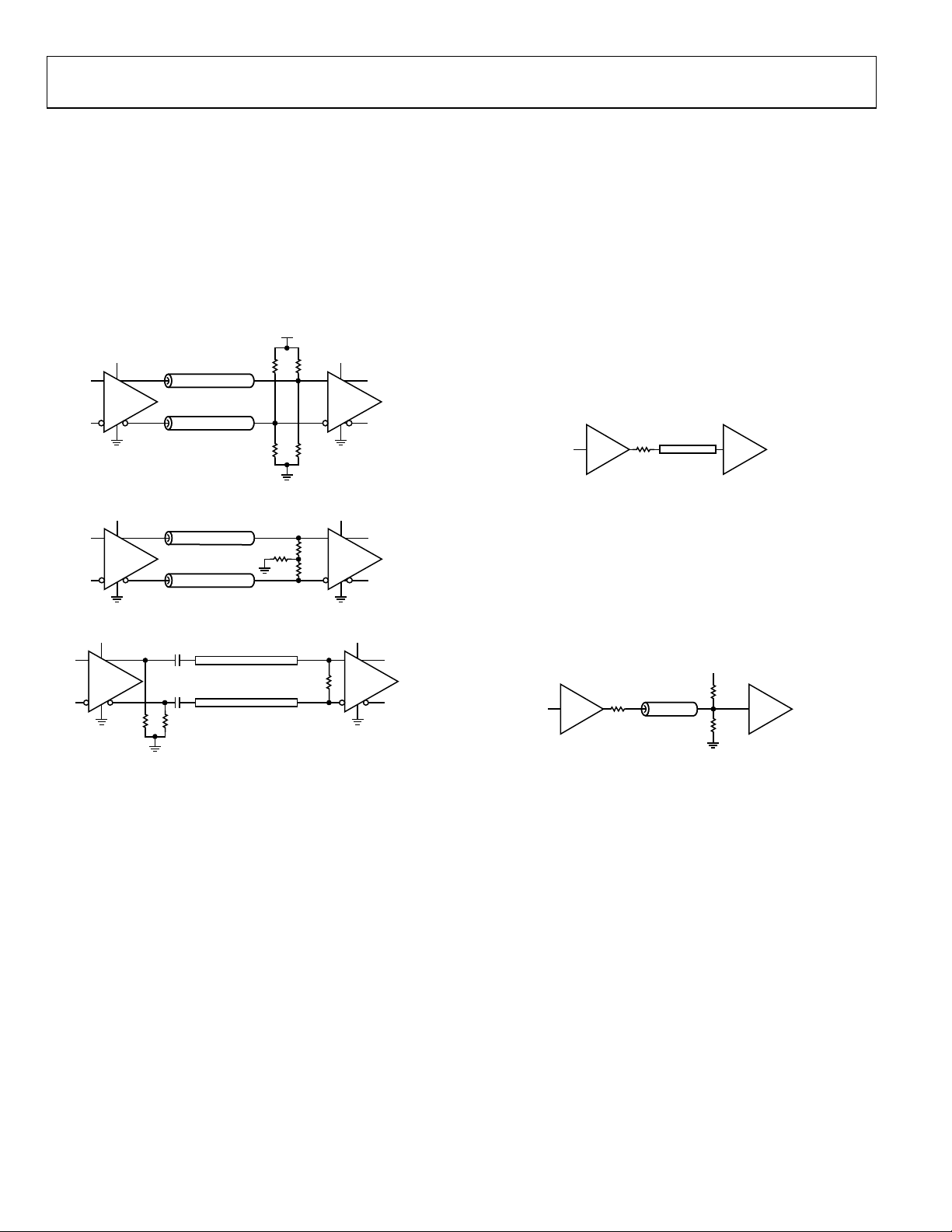
AD9520-5
V
V
V
V
V
V
Ω
V
http://www.BDTIC.com/ADI
Thevenin-equivalent termination uses a resistor network to
provide 50 Ω termination to a dc voltage that is below V
of
OL
the LVPECL driver. In this case, VS_DRV on the AD9520
should equal V
of the receiving buffer. Although the resistor
S
combination shown results in a dc bias point of VS_DRV − 2 V,
the actual common-mode voltage is VS_DRV − 1.3 V because
there is additional current flowing from the AD9520 LVPECL
driver through the pull-down resistor.
The circuit is identical for the case where VS_DRV = 2.5 V, except
that the pull-down resistor is 62.5 Ω and the pull-up is 250 Ω.
S_DRV
VS_DRV
LVPECL
50Ω
SINGLE-ENDED
(NOT COUPL ED)
50Ω
V
S
127Ω127Ω
LVPECL
83Ω83Ω
7239-045
Figure 58. DC-Coupled 3.3 V LVPECL Far-End Thevenin Termination
S_DRV
LVPECL
Z0 = 50Ω
50Ω
Z0 = 50Ω
50Ω
50Ω
= VS_DR
S
LVPECL
7239-047
Figure 59. DC-Coupled 3.3 V LVPECL Y-Termination
S_DRV
LVPECL
200Ω 200Ω
0.1nF
100Ω DIFFERENTIAL
0.1nF
TRANSMISSION LINE
(COUPLED)
100Ω
S
LVPECL
07239-046
Figure 60. AC-Coupled LVPECL with Parallel Transmission Line
CMOS CLOCK DISTRIBUTION
The output drivers of the AD9520 can be configured as CMOS
drivers. When selected as a CMOS driver, each output becomes
a pair of CMOS outputs, each of which can be individually
turned on or off and set as inverting or noninverting. These
outputs are 3.3 V or 2.5 V CMOS compatible. However, every
output driver (including the LVPECL drivers) must be run at
either 2.5 V or 3.3 V. The user cannot mix and match 2.5 V and
3.3 V outputs.
When single-ended CMOS clocking is used, some of the
following guidelines apply.
Point-to-point connections should be designed such that each
driver has only one receiver, if possible. Connecting outputs in
this manner allows for simple termination schemes and minimizes
ringing due to possible mismatched impedances on the output
trace. Series termination at the source is generally required to
provide transmission line matching and/or to reduce current
transients at the driver.
The value of the resistor is dependent on the board design and
timing requirements (typically 10 Ω to 100 Ω is used). CMOS
outputs are also limited in terms of the capacitive load or trace
length that they can drive. Typically, trace lengths less than
3 inches are recommended to preserve signal rise/fall times and
signal integrity.
60.4
(1.0 INCH)
10Ω
CMOS CMOS
MICROSTRIP
07239-076
Figure 61. Series Termination of CMOS Output
Termination at the far end of the PCB trace is a second option.
The CMOS outputs of the AD9520 do not supply enough current
to provide a full voltage swing with a low impedance resistive, farend termination, as shown in Figure 62. The far-end termination
network should match the PCB trace impedance and provide the
desired switching point. The reduced signal swing may still meet
receiver input requirements in some applications. This can be
useful when driving long trace lengths on less critical nets.
S
10Ω
CMOS CMOS
50Ω
100Ω
100Ω
7239-077
Figure 62. CMOS Output with Far-End Termination
Because of the limitations of single-ended CMOS clocking,
consider using differential outputs when driving high speed
signals over long traces. The AD9520 offers LVPECL outputs
that are better suited for driving long traces where the inherent
noise immunity of differential signaling provides superior
performance for clocking converters.
Rev. 0 | Page 76 of 80

AD9520-5
http://www.BDTIC.com/ADI
OUTLINE DIMENSIONS
49
48
0.60 MAX
EXPOSED PAD
(BOTTOM VIEW)
PIN 1
64
INDICATOR
1
6.35
6.20 SQ
6.05
PIN 1
INDICATOR
9.00
BSC SQ
TOP VIE W
8.75
BSC SQ
0.60
MAX
0.50
BSC
1.00
0.85
0.80
SEATING
PLANE
12° MAX
0.50
0.40
0.30
0.80 MAX
0.65 TYP
0.30
0.23
0.18
COMPLIANT TO JEDEC STANDARDS MO-220-VMMD-4
0.05 MAX
0.02 NOM
0.20 REF
33
32
7.50
REF
16
17
FOR PROPER CO NNECTION O F
THE EXPOSED PAD, REFER TO
THE PIN CONF IGURATIO N AND
FUNCTION DESCRI PTIONS
SECTION OF THIS DATA SHEET.
0.25 MIN
091707-C
Figure 63. 64-Lead Lead Frame Chip Scale Package [LFCSP_VQ]
9 mm × 9 mm Body, Very Thin Quad
CP-64-4
Dimensions shown in millimeters
ORDERING GUIDE
Model Temperature Range Package Description Package Option
AD9520-5BCPZ
AD9520-5BCPZ-REEL7
AD9520-5/PCBZ
1
Z = RoHS Compliant Part.
1
1
Evaluation Board
−40°C to +85°C 64-Lead Lead Frame Chip Scale Package (LFCSP_VQ) CP-64-4
1
−40°C to +85°C 64-Lead Lead Frame Chip Scale Package (LFCSP_VQ) CP-64-4
Rev. 0 | Page 77 of 80
 Loading...