ANALOG DEVICES AD9520-1 Service Manual
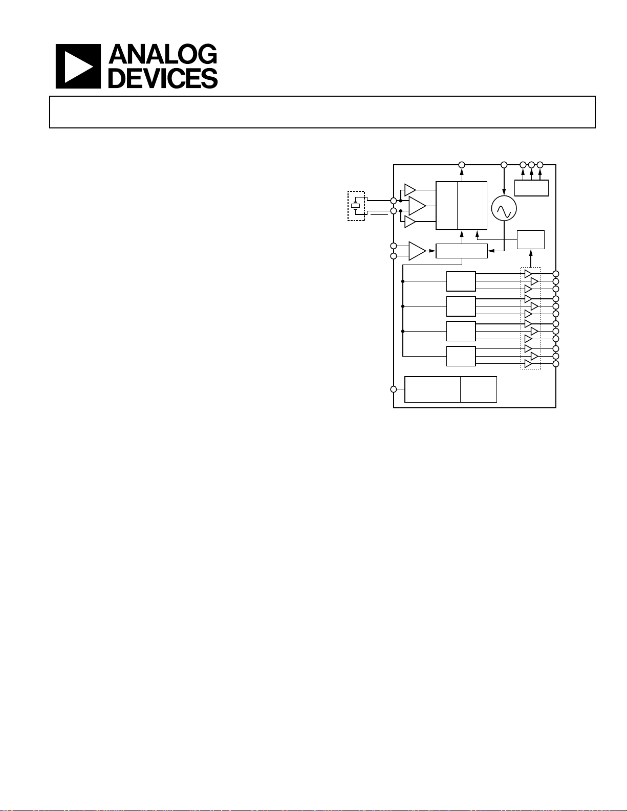
12 LVPECL/24 CMOS Output Clock
FEATURES
Low phase noise, phase-locked loop (PLL)
Generator with Integrated 2.5 GHz VCO
AD9520-1
FUNCTIONAL BLOCK DIAGRAM
CP
LF
On-chip VCO tunes from 2.27 GHz to 2.65 GHz
VCO
LVPECL/
CMOS
STATUS
MONITOR
ZERO
DELAY
Supports external 3.3 V/5 V VCO/VCXO to 2.4 GHz
1 differential or 2 single-ended reference inputs
Accepts CMOS, LVDS, or LVPECL references to 250 MHz
Accepts 16.67 MHz to 33.3 MHz crystal for reference input
Optional reference clock doubler
Reference monitoring capability
Auto and manual reference switchover/holdover modes,
with selectable revertive/nonrevertive switching
Glitch-free switchover between references
OPTIONAL
REFIN
REFIN
CLK
REF1
REF2
SWITCHOVER
AND MONITOR
DIVIDER
AND MUXES
DIV/Φ
PLL
Automatic recovery from holdover
Digital or analog lock detect, selectable
DIV/Φ
Optional zero delay operation
Twelve 1.6 GHz LVPECL outputs divided into 4 groups
DIV/Φ
Each group of 3 has a 1-to-32 divider with phase delay
Additive output jitter as low as 225 fs rms
DIV/Φ
Channel-to-channel skew grouped outputs <16 ps
Each LVPECL output can be configured as 2 CMOS outputs
(for f
≤ 250 MHz)
OUT
SPI/I2C CONTRO L
PORT AND
DIGITAL LOGIC
EEPROM
AD9520
Automatic synchronization of all outputs on power-up
Manual synchronization of outputs as needed
SPI- and I²C-compatible serial control port
64-lead LFCSP
Nonvolatile EEPROM stores configuration settings
APPLICATIONS
Low jitter, low phase noise clock distribution
Clock generation and translation for SONET, 10Ge, 10G FC,
and other 10 Gbps protocols
Forward error correction (G.710)
Clocking high speed ADCs, DACs, DDSs, DDCs, DUCs, MxFEs
High performance wireless transceivers
ATE and high performance instrumentation
Broadband infrastructures
GENERAL DESCRIPTION
The AD9520-11 provides a multioutput clock distribution
The AD9520 serial interface supports both SPI and IC® ports.
An in-package EEPROM can be programmed through the
serial interface and store user-defined register settings for
power-up and chip reset.
The AD9520 features 12 LVPECL outputs in four groups. Any
of the 1.6 GHz LVPECL outputs can be reconfigured as two
250 MHz CMOS outputs.
Each group of outputs has a divider that allows both the divide
ratio (from 1 to 32) and the phase (coarse delay) to be set.
The AD9520 is available in a 64-lead LFCSP and can be operated
from a single 3.3 V supply. The external VCO can have an
operating voltage up to 5.5 V. A separate output driver power
supply can be from 2.375 V to 3.465 V.
The AD9520 is specified for operation over the standard industrial
range of −40°C to +85°C.
Figure 1.
function with subpicosecond jitter performance, along with an
on-chip PLL and VCO. The on-chip VCO tunes from 2.27 GHz
to 2.65 GHz. An external 3.3 V/5 V VCO/VCXO of up to 2.4 GHz
can also be used.
1
The AD9520 is used throughout this data sheet to refer to all the members of the AD9520 family. However, when AD9520-1 is used, it is referring to that specific
member of the AD9520 family.
OUT0
OUT1
OUT2
OUT3
OUT4
OUT5
OUT6
OUT7
OUT8
OUT9
OUT10
OUT11
07214-001
Rev. 0
Information furnished by Analog Devices is believed to be accurate and reliable. However, no
responsibility is assumed by Analog Devices for its use, nor for any infringements of patents or other
rights of third parties that may result from its use. Specifications subject to change without notice. No
license is granted by implication or otherwise under any patent or patent rights of Analog Devices.
Trademarks and registered trademarks are the property of their respective owners.
One Technology Way, P.O. Box 9106, Norwood, MA 02062-9106, U.S.A.
Tel: 781.329.4700 www.analog.com
Fax: 781.461.3113 ©2008 Analog Devices, Inc. All rights reserved.

AD9520-1
TABLE OF CONTENTS
Features .............................................................................................. 1
Applications ....................................................................................... 1
General Description ......................................................................... 1
Functional Block Diagram .............................................................. 1
Revision History ............................................................................... 3
Specifications ..................................................................................... 4
Power Supply Requirements ....................................................... 4
PLL Characteristics ...................................................................... 4
Clock Inputs .................................................................................. 7
Clock Outputs ............................................................................... 7
Timing Characteristics ................................................................ 8
Timing Diagrams ..................................................................... 9
Clock Output Additive Phase Noise (Distribution Only;
VCO Divider Not Used) ............................................................ 10
Clock Output Absolute Phase Noise (Internal VCO Used) .. 11
Clock Output Absolute Time Jitter (Clock Generation
Using Internal VCO) .................................................................. 11
Clock Output Absolute Time Jitter (Clock Cleanup
Using Internal VCO) .................................................................. 11
Clock Output Absolute Time Jitter (Clock Generation
Using External VCXO) .............................................................. 12
Clock Output Additive Time Jitter
(VCO Divider Not Used) .......................................................... 12
Clock Output Additive Time Jitter (VCO Divider Used) ..... 13
Serial Control Port—SPI Mode ................................................ 13
Serial Control Port—IC Mode ................................................ 14
SYNC
PD
,
Serial Port Setup Pins: SP1, SP0 ............................................... 15
LD, STATUS, and REFMON Pins ............................................ 15
Power Dissipation ....................................................................... 16
Absolute Maximum Ratings .......................................................... 17
Thermal Resistance .................................................................... 17
ESD Caution ................................................................................ 17
Pin Configuration and Function Descriptions ........................... 18
Typical Performance Characteristics ........................................... 21
Terminolog y .................................................................................... 26
Detailed Block Diagram ................................................................ 27
, and
RESET
Pins ..................................................... 15
Theory of Operation ...................................................................... 28
Operational Configurations ...................................................... 28
Mode 0: Internal VCO and Clock Distribution ................. 28
Mode 1: Clock Distribution or External
VCO < 1600 MHz .................................................................. 30
Mode 2: High Frequency Clock Distribution—CLK or
External VCO > 1600 MHz .................................................. 32
Phase-Locked Loop (PLL) .................................................... 34
Configuration of the PLL ...................................................... 34
Phase Frequency Detector (PFD) ........................................ 34
Charge Pump (CP) ................................................................. 35
On-Chip VCO ........................................................................ 35
PLL External Loop Filter ....................................................... 35
PLL Reference Inputs ............................................................. 35
Reference Switchover ............................................................. 36
Reference Divider R ............................................................... 36
VCO/VCXO Feedback Divider N: P, A, B, R ..................... 36
Digital Lock Detect (DLD) ................................................... 38
Analog Lock Detect (ALD) ................................................... 38
Current Source Digital Lock Detect (CSDLD) .................. 38
External VCXO/VCO Clock Input (CLK/
Holdover .................................................................................. 39
External/Manual Holdover Mode ........................................ 39
Automatic/Internal Holdover Mode .................................... 39
Frequency Status Monitors ................................................... 41
VCO Calibration .................................................................... 42
Zero Delay Operation ................................................................ 43
Internal Zero Delay Mode ..................................................... 43
External Zero Delay Mode .................................................... 43
Clock Distribution ..................................................................... 44
Operation Modes ................................................................... 44
CLK or VCO Direct-to-LVPECL Outputs .......................... 44
Clock Frequency Division ..................................................... 45
VCO Divider ........................................................................... 45
Channel Dividers ................................................................... 45
Synchronizing the Outputs—
LVPECL Output Drivers ....................................................... 49
CMOS Output Drivers .......................................................... 49
SYNC
CLK
) ................ 39
Function ................... 47
Rev. 0 | Page 2 of 84

AD9520-1
Reset Modes ................................................................................. 49
Power-On Reset ....................................................................... 49
Hardware Reset via the
Soft Reset via the Serial Port.................................................. 50
Soft Reset to Settings in EEPROM when
EEPROM Pin = 0 via the Serial Port ...................................... 50
Power-Down Modes ................................................................... 50
Chip Power-Down via PD ..................................................... 50
PLL Power-Down .................................................................... 50
Distribution Power-Down ..................................................... 50
Individual Clock Output Power-Down ................................ 50
Individual Clock Channel Power-Down ............................. 50
Serial Control Port .......................................................................... 51
SPI/IC Port Selection ................................................................ 51
IC Serial Port Operation ........................................................... 51
I2C Bus Characteristics ........................................................... 51
Data Transfer Process ............................................................. 52
Data Transfer Format ............................................................. 53
IC Serial Port Timing ............................................................ 53
SPI Serial Port Operation ........................................................... 54
Pin Descriptions ...................................................................... 54
SPI Mode Operation ............................................................... 54
Communication Cycle—Instruction Plus Data .................. 54
Write ......................................................................................... 54
Read .......................................................................................... 54
RESET
Pin ...................................... 49
SPI Instruction Word (16 Bits) .................................................. 55
SPI MSB/LSB First Transfers ..................................................... 55
EEPROM Operations ..................................................................... 58
Writing to the EEPROM ............................................................ 58
Reading from the EEPROM ...................................................... 58
Programming the EEPROM Buffer Segment.......................... 59
Register Section Definition Group ....................................... 59
IO_UPDATE (Operational Code 0x80) .............................. 59
End-of-Data (Operational Code 0xFF) ............................... 59
Pseudo-End-of-Data (Operational Code 0xFE) ................. 59
Thermal Performance ..................................................................... 61
Register Map .................................................................................... 62
Register Map Descriptions ............................................................. 67
Applications Information ............................................................... 82
Frequency Planning Using the AD9520 .................................. 82
Using the AD9520 Outputs for ADC Clock Applications .... 82
LVPECL Clock Distribution ...................................................... 82
CMOS Clock Distribution ......................................................... 83
Outline Dimensions ........................................................................ 84
Ordering Guide ........................................................................... 84
REVISION HISTORY
9/08—Revision 0: Initial Version
Rev. 0 | Page 3 of 84
AD9520-1
SPECIFICATIONS
Typical (typ) is given for VS = VS_DRV = 3.3 V ± 5%; VS ≤ VCP ≤ 5.25 V; TA = 25°C; RSET = 4.12 kΩ; CPRSET = 5.1 kΩ, unless otherwise
noted. Minimum (min) and maximum (max) values are given over full VS and T
POWER SUPPLY REQUIREMENTS
Table 1.
Parameter Min Typ Max Unit Test Conditions/Comments
VS 3.135 3.3 3.465 V 3.3 V ± 5%
VS_DRV 2.375 VS V This is nominally 2.5 V to 3.3 V ± 5%
VCP VS 5.25 V This is nominally 3.3 V to 5.0 V ± 5%
RSET Pin Resistor 4.12 kΩ Sets internal biasing currents; connect to ground
CPRSET Pin Resistor 5.1 kΩ
Sets internal CP current range, nominally 4.8 mA (CP_lsb = 600 μA);
actual current can be calculated by CP_lsb = 3.06/CPRSET; connect to ground
BYPASS Pin Capacitor 220 nF Bypass for internal LDO regulator; necessary for LDO stability; connect to ground
PLL CHARACTERISTICS
Table 2.
Parameter Min Typ Max Unit Test Conditions/Comments
VCO (ON-CHIP)
Frequency Range 2270 2650 MHz See Figure 13
VCO Gain (K
Tunin g Volt age (VT) 0.5
Frequency Pushing (Open-Loop) 1 MHz/V
Phase Noise @ 1 kHz Offset −50 dBc/Hz f = 2475 MHz
Phase Noise @ 100 kHz Offset −107 dBc/Hz f = 2475 MHz
Phase Noise @ 1 MHz Offset −126 dBc/Hz f = 2475 MHz
REFERENCE INPUTS
Differential Mode (REFIN, REFIN)
Input Frequency 0 250 MHz
Input Sensitivity 280 mV p-p
Self-Bias Voltage, REFIN 1.34 1.60 1.75 V Self-bias voltage of REFIN
Self-Bias Voltage, REFIN
Input Resistance, REFIN 4.0 4.8 5.9 kΩ Self-biased
Input Resistance, REFIN
Dual Single-Ended Mode (REF1, REF2) Two single-ended CMOS-compatible inputs
Input Frequency (AC-Coupled)
with DC Offset Off)
Input Frequency (AC-Coupled
with DC Offset On)
Input Frequency (DC-Coupled) 0 250 MHz Slew rate > 50 V/μs; CMOS levels
Input Sensitivity (AC-Coupled
with DC Offset Off)
Input Sensitivity (AC-Coupled
with DC Offset On)
Input Logic High, DC Offset Off 2.0 V
Input Logic Low, DC Offset Off 0.8 V
Input Current −100 +100 μA
Input Capacitance 2 pF
) 50 MHz/V See Figure 8
VCO
VCP −
0.5
1.30 1.50 1.60 V
4.4 5.3 6.4 kΩ Self-biased
10 250 MHz Slew rate must be > 50 V/μs
250 MHz
0.55 3.28 V p-p VIH should not exceed VS
1.5 2.78 V p-p VIH should not exceed VS
(−40°C to +85°C) variation.
A
V VCP ≤ VS when using internal VCO
Differential mode (can accommodate single-ended
input by ac grounding undriven input)
Frequencies below about 1 MHz should be dc-coupled;
be careful to match V
Self-bias voltage of REFIN
1
1
(self-bias voltage)
CM
1
1
Slew rate must be > 50 V/μs, and input amplitude
sensitivity specification must be met; see input sensitivity
Each pin, REFIN (REF1)/REFIN
(REF2)
Rev. 0 | Page 4 of 84

AD9520-1
Parameter Min Typ Max Unit Test Conditions/Comments
Crystal Oscillator
Crystal Resonator Frequency Range 16.67 33.33 MHz
Maximum Crystal Motional Resistance 30 Ω
PHASE/FREQUENCY DETECTOR (PFD)
PFD Input Frequency 100 MHz Antibacklash pulse width = 1.3 ns, 2.9 ns
45 MHz Antibacklash pulse width = 6.0 ns
Reference Input Clock Doubler Frequency 0.004 50 MHz Antibacklash pulse width = 1.3 ns, 2.9 ns
Antibacklash Pulse Width 1.3 ns 0x017[1:0] = 01b
2.9 ns 0x017[1:0] = 00b; 0x017[1:0] = 11b
6.0 ns 0x017[1:0] = 10b
CHARGE PUMP (CP)
ICP Sink/Source Programmable
High Value 4.8 mA
With CPRSET = 5.1 kΩ; higher I
changing CPRSET
Low Value 0.60 mA
With CPRSET = 5.1 kΩ; lower I
changing CPRSET
Absolute Accuracy 2.5 % Charge pump voltage set to VCP/2
CPRSET Range 2.7 10 kΩ
ICP High Impedance Mode Leakage 1 nA
Sink-and-Source Current Matching 1 %
0.5 V < V
< VCP − 0.5 V; VCP is the voltage on the CP (charge
CP
pump) pin; VCP is the voltage on the VCP power supply pin
ICP vs. VCP 1.5 % 0.5 V < VCP < VCP − 0.5 V
ICP vs. Temperature 2 % VCP = VCP/2 V
PRESCALER (PART OF N DIVIDER)
Prescaler Input Frequency
P = 1 FD 300 MHz
P = 2 FD 600 MHz
P = 3 FD 900 MHz
P = 2 DM (2/3) 600 MHz
P = 4 DM (4/5) 1000 MHz
P = 8 DM (8/9) 2400 MHz
P = 16 DM (16/17) 3000 MHz
P = 32 DM (32/33) 3000 MHz
Prescaler Output Frequency 300 MHz
A, B counter input frequency (prescaler input frequency
divided by P)
PLL N DIVIDER DELAY Register 0x019[2:0]; see Table 53
000 Off
001 410 ps
010 530 ps
011 650 ps
100 770 ps
101 890 ps
110 1010 ps
111 1130 ps
PLL R DIVIDER DELAY Register 0x019[5:3]; see Table 53
000 Off
001 370 ps
010 490 ps
011 610 ps
100 730 ps
101 850 ps
110 970 ps
111 1090 ps
is possible by
CP
is possible by
CP
Rev. 0 | Page 5 of 84

AD9520-1
Parameter Min Typ Max Unit Test Conditions/Comments
PHASE OFFSET IN ZERO DELAY
Phase Offset (REF-to-LVPECL Clock Output
560 1060 1310 ps When N delay and R delay are bypassed
REF refers to REFIN (REF1)/REFIN
Pins) in Internal Zero Delay Mode
Phase Offset (REF-to-LVPECL Clock Output
−320 +50 +240 ps When N delay = Setting 110 and R delay is bypassed
Pins) in Internal Zero Delay Mode
Phase Offset (REF-to-CLK Input Pins) in
140 630 870 ps When N delay and R delay are bypassed
External Zero Delay Mode
Phase Offset (REF-to-CLK Input Pins) in
−460 −20 +200 ps When N delay = Setting 011 and R delay is bypassed
External Zero Delay Mode
NOISE CHARACTERISTICS
In-Band Phase Noise of the Charge Pump/
Phase Frequency Detector (In-Band
Means Within the LBW of the PLL)
The PLL in-band phase noise floor is estimated by
measuring the in-band phase noise at the output of
the VCO and subtracting 20 log(N) (where N is the value
of the N divider)
@ 500 kHz PFD Frequency −165 dBc/Hz
@ 1 MHz PFD Frequency −162 dBc/Hz
@ 10 MHz PFD Frequency −152 dBc/Hz
@ 50 MHz PFD Frequency −144 dBc/Hz
PLL Figure of Merit (FOM) −222 dBc/Hz
Reference slew rate > 0.5 V/ns; FOM + 10 log(f
approximation of the PFD/CP in-band phase noise (in
the flat region) inside the PLL loop bandwidth; when
running closed-loop, the phase noise, as observed at
the VCO output, is increased by 20 log(N); PLL figure of
merit decreases with decreasing slew rate; see Figure 12
PLL DIGITAL LOCK DETECT WINDOW
2
Signal available at the LD, STATUS, and REFMON pins
when selected by appropriate register settings; lock
detect window settings can be varied by changing the
CPRSET resistor
Lock Threshold (Coincidence of Edges)
Selected by 0x017[1:0] and 0x018[4] (this is the threshold
to go from unlock to lock)
Low Range (ABP 1.3 ns, 2.9 ns) 3.5 ns 0x017[1:0] = 00b, 01b, 11b; 0x018[4] = 1b
High Range (ABP 1.3 ns, 2.9 ns) 7.5 ns 0x017[1:0] = 00b, 01b, 11b; 0x018[4] = 0b
High Range (ABP 6.0 ns) 3.5 ns 0x017[1:0] = 10b; 0x018[4] = 0b
Unlock Threshold (Hysteresis)
2
Selected by 0x017[1:0] and 0x018[4] (this is the threshold
to go from lock to unlock)
Low Range (ABP 1.3 ns, 2.9 ns) 7 ns 0x017[1:0] = 00b, 01b, 11b; 0x018[4] = 1b
High Range (ABP 1.3 ns, 2.9 ns) 15 ns 0x017[1:0] = 00b, 01b, 11b; 0x018[4] = 0b
High Range (ABP 6.0 ns) 11 ns 0x017[1:0] = 10b; 0x018[4] = 0b
1
The REFIN and
2
For reliable operation of the digital lock detect, the period of the PFD frequency must be greater than the unlock-after-lock time.
REFIN
self-bias points are offset slightly to avoid chatter on an open input condition.
(REF2)
PFD
) is an
Rev. 0 | Page 6 of 84
AD9520-1
CLOCK INPUTS
Table 3.
Parameter Min Typ Max Unit Test Conditions/Comments
CLOCK INPUTS (CLK, CLK)
Input Frequency 0
0
Input Sensitivity, Differential 150 mV p-p
Input Level, Differential 2 V p-p
Input Common-Mode Voltage, VCM 1.3 1.57 1.8 V Self-biased; enables ac coupling
Input Common-Mode Range, V
1.3 1.8 V With 200 mV p-p signal applied; dc-coupled
CMR
Input Sensitivity, Single-Ended 150 mV p-p
Input Resistance 3.9 4.7 5.7 kΩ Self-biased
Input Capacitance 2 pF
1
Below about 1 MHz, the input should be dc-coupled. Care should be taken to match VCM.
CLOCK OUTPUTS
Table 4.
Parameter Min Typ Max Unit Test Conditions/Comments
LVPECL CLOCK OUTPUTS Termination = 50 Ω to VS_DRV − 2 V
OUT0, OUT1, OUT2, OUT3, OUT4,
OUT5, OUT6, OUT7, OUT8,
OUT9, OUT10, OUT11
Output Frequency, Maximum 2400 MHz
Output High Voltage, VOH
Output Low Voltage, VOL
Output Differential Voltage, VOD 660 820 950 mV
CMOS CLOCK OUTPUTS
OUT0A, OUT0B, OUT1A, OUT1B,
OUT2A, OUT2B, OUT3A, OUT3B,
OUT4A, OUT4B, OUT5A, OUT5B,
OUT6A, OUT6B, OUT7A, OUT7B,
OUT8A, OUT8B, OUT9A, OUT9B,
OUT10A, OUT10B, OUT11A,
OUT11B
Output Frequency 250 MHz See Figure 22
Output Voltage High, VOH VS − 0.1 V @ 1 mA load, VS_DRV = 3.3 V/2.5 V
Output Voltage Low, VOL 0.1 V @ 1 mA load, VS_DRV = 3.3 V/2.5 V
Output Voltage High, VOH 2.7 V @ 10 mA load, VS_DRV = 3.3 V
Output Voltage Low, VOL 0.5 V @ 10 mA load, VS_DRV = 3.3 V
Output Voltage High, VOH 1.8 V @ 10 mA load, VS_DRV = 2.5 V
Output Voltage Low, VOL 0.6 V @ 10 mA load, VS_DRV = 2.5 V
Differential input
1
2.4 GHz High frequency distribution (VCO divider)
1
1.6 GHz
Distribution only (VCO divider bypassed); this is the
frequency range supported by the channel divider
Measured at 2.4 GHz; jitter performance is improved with
slew rates > 1 V/ns
Larger voltage swings can turn on the protection diodes
and can degrade jitter performance
CLK ac-coupled; CLK
Differential (OUT, OUT)
ac-bypassed to RF ground
Using direct to output; see Figure 21 (higher
frequencies are possible, but amplitude will
not meet the V
specification); the maximum
OD
output frequency is limited by either the
maximum VCO frequency or the frequency at
the CLK inputs, depending on the AD9520
configuration
VS_DRV −
1.07
VS_DRV −
1.95
VS_DRV −
0.96
VS_DRV −
1.79
VS_DRV −
0.84
VS_DRV −
1.64
V
V
Single-ended; termination = 10 pF
Rev. 0 | Page 7 of 84

AD9520-1
TIMING CHARACTERISTICS
Table 5.
Parameter Min Typ Max Unit Test Conditions/Comments
LVPECL OUTPUT RISE/FALL TIMES Termination = 50 Ω to VS_DRV − 2 V
Output Rise Time, tRP 130 170 ps
Output Fall Time, tFP 130 170 ps
PROPAGATION DELAY, t
, CLK-TO-LVPECL OUTPUT
PECL
For All Divide Values 850 1050 1280 ps High frequency clock distribution configuration
800 970 1180 ps Clock distribution configuration
Variation with Temperature 1.0 ps/°C
OUTPUT SKEW, LVPECL OUTPUTS
1
Termination = 50 Ω to VS_DRV − 2 V
LVPECL Outputs That Share the Same Divider 5 16 ps VS_DRV = 3.3 V
5 20 ps VS_DRV = 2.5 V
LVPECL Outputs on Different Dividers 5 45 ps VS_DRV = 3.3 V
5 60 ps VS_DRV = 2.5 V
All LVPECL Outputs Across Multiple Parts 190 ps VS_DRV = 3.3 V and 2.5 V
CMOS OUTPUT RISE/FALL TIMES Termination = open
Output Rise Time, tRC 750 960 ps 20% to 80%; C
Output Fall Time, tFC 715 890 ps 80% to 20%; C
Output Rise Time, tRC 965 1280 ps 20% to 80%; C
Output Fall Time, tFC 890 1100 ps 80% to 20%; C
PROPAGATION DELAY, t
, CLK-TO-CMOS OUTPUT Clock distribution configuration
CMOS
For All Divide Values 2.1 2.75 3.55 ns VS_DRV = 3.3 V
3.35 ns VS_DRV = 2.5 V
Variation with Temperature 2 ps/°C VS_DRV = 3.3 V and 2.5 V
OUTPUT SKEW, CMOS OUTPUTS
1
CMOS Outputs That Share the Same Divider 7 85 ps VS_DRV = 3.3 V
10 105 ps VS_DRV = 2.5 V
All CMOS Outputs on Different Dividers 10 240 ps VS_DRV = 3.3 V
10 285 ps VS_DRV = 2.5 V
All CMOS Outputs Across Multiple Parts 600 ps VS_DRV = 3.3 V
620 ps VS_DRV = 2.5 V
OUTPUT SKEW, LVPECL-TO-CMOS OUTPUT
1
All settings identical; different logic type
Outputs That Share the Same Divider 1.18 1.76 2.48 ns LVPECL to CMOS on same part
Outputs That Are on Different Dividers 1.20 1.78 2.50 ns LVPECL to CMOS on same part
1
The output skew is the difference between any two similar delay paths while operating at the same voltage and temperature.
20% to 80%, measured differentially (rise/fall
times are independent of VS and are valid for
VS_DRV = 3.3 V and 2.5 V)
80% to 20%, measured differentially (rise/fall
times are independent of VS and are valid for
VS_DRV = 3.3 V and 2.5 V)
= 10 pF; VS_DRV = 3.3 V
LOAD
= 10 pF; VS_DRV = 3.3 V
LOAD
= 10 pF; VS_DRV = 2.5 V
LOAD
= 10 pF; VS_DRV = 2.5 V
LOAD
Rev. 0 | Page 8 of 84
AD9520-1
K
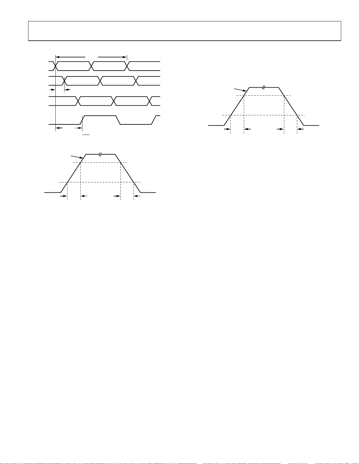
Timing Diagrams
t
CLK
CL
t
t
CMOS
Figure 2. CLK/
DIFFERENTIAL
80%
20%
t
PECL
CLK
to Clock Output Timing, Div = 1
LVPECL
RP
07214-060
t
FP
07214-061
SINGL E-ENDE D
80%
CMOS
10pF LOAD
20%
t
RC
t
FC
Figure 4. CMOS Timing, Single-Ended, 10 pF Load
07214-063
Figure 3. LVPECL Timing, Differential
Rev. 0 | Page 9 of 84

AD9520-1
CLOCK OUTPUT ADDITIVE PHASE NOISE (DISTRIBUTION ONLY; VCO DIVIDER NOT USED)
Table 6.
Parameter Min Typ Max Unit Test Conditions/Comments
CLK-TO-LVPECL ADDITIVE PHASE NOISE
CLK = 1 GHz, Output = 1 GHz Input slew rate > 1 V/ns
Divider = 1
@ 10 Hz Offset −107 dBc/Hz
@ 100 Hz Offset −117 dBc/Hz
@ 1 kHz Offset −127 dBc/Hz
@ 10 kHz Offset −135 dBc/Hz
@ 100 kHz Offset −142 dBc/Hz
@ 1 MHz Offset −145 dBc/Hz
@ 10 MHz Offset −147 dBc/Hz
@ 100 MHz Offset −150 dBc/Hz
CLK = 1 GHz, Output = 200 MHz Input slew rate > 1 V/ns
Divider = 5
@ 10 Hz Offset −122 dBc/Hz
@ 100 Hz Offset −132 dBc/Hz
@ 1 kHz Offset −143 dBc/Hz
@ 10 kHz Offset −150 dBc/Hz
@ 100 kHz Offset −156 dBc/Hz
@ 1 MHz Offset −157 dBc/Hz
>10 MHz Offset −157 dBc/Hz
CLK-TO-CMOS ADDITIVE PHASE NOISE
CLK = 1 GHz, Output = 250 MHz Input slew rate > 1 V/ns
Divider = 4
@ 10 Hz Offset −107 dBc/Hz
@ 100 Hz Offset −119 dBc/Hz
@ 1 kHz Offset −125 dBc/Hz
@ 10 kHz Offset −134 dBc/Hz
@ 100 kHz Offset −144 dBc/Hz
@ 1 MHz Offset −148 dBc/Hz
>10 MHz Offset −154 dBc/Hz
CLK = 1 GHz, Output = 50 MHz Input slew rate > 1 V/ns
Divider = 20
@ 10 Hz Offset −126 dBc/Hz
@ 100 Hz Offset −133 dBc/Hz
@ 1 kHz Offset −140 dBc/Hz
@ 10 kHz Offset −148 dBc/Hz
@ 100 kHz Offset −157 dBc/Hz
@ 1 MHz Offset −160 dBc/Hz
>10 MHz Offset −163 dBc/Hz
Distribution section only; does not include
PLL and VCO
Distribution section only; does not include
PLL and VCO
Rev. 0 | Page 10 of 84
AD9520-1
CLOCK OUTPUT ABSOLUTE PHASE NOISE (INTERNAL VCO USED)
Table 7.
Parameter Min Typ Max Unit Test Conditions/Comments
LVPECL ABSOLUTE PHASE NOISE
VCO = 2.65 GHz; Output = 2.65 GHz
@ 1 kHz Offset −49 dBc/Hz
@ 10 kHz Offset −80 dBc/Hz
@ 100 kHz Offset −105 dBc/Hz
@ 1 MHz Offset −125 dBc/Hz
@ 10 MHz Offset −140 dBc/Hz
@ 40 MHz Offset −146 dBc/Hz
VCO = 2.475 GHz; Output = 2.475 GHz
@ 1 kHz Offset −50 dBc/Hz
@ 10 kHz Offset −82 dBc/Hz
@ 100 kHz Offset −107 dBc/Hz
@ 1 MHz Offset −126 dBc/Hz
@ 10 MHz Offset −141 dBc/Hz
@ 40 MHz Offset −146 dBc/Hz
VCO = 2.3 GHz; Output = 2.3 GHz
@ 1 kHz Offset −54 dBc/Hz
@ 10 kHz Offset −84 dBc/Hz
@ 100 kHz Offset −109 dBc/Hz
@ 1 MHz Offset −128 dBc/Hz
@ 10 MHz Offset −142 dBc/Hz
@ 40 MHz Offset −146 dBc/Hz
Internal VCO; direct-to-LVPECL output and for
loop bandwidths < 1 kHz
CLOCK OUTPUT ABSOLUTE TIME JITTER (CLOCK GENERATION USING INTERNAL VCO)
Table 8.
Parameter Min Typ Max Unit Test Conditions/Comments
LVPECL OUTPUT ABSOLUTE TIME JITTER
VCO = 2.458 GHz; LVPECL = 245.76 MHz; PLL LBW = 55 kHz 152 fs rms Integration BW = 200 kHz to 10 MHz
328 fs rms Integration BW = 12 kHz to 20 MHz
VCO = 2.458 GHz; LVPECL = 122.88 MHz; PLL LBW = 55 kHz 155 fs rms Integration BW = 200 kHz to 10 MHz
323 fs rms Integration BW = 12 kHz to 20 MHz
VCO = 2.458 GHz; LVPECL = 61.44 MHz; PLL LBW = 55 kHz 173 fs rms Integration BW = 200 kHz to 10 MHz
336 fs rms Integration BW = 12 kHz to 20 MHz
Application example based on a typical
setup where the reference source is
clean, so a wider PLL loop bandwidth is
used; reference = 15.36 MHz; R DIV = 1
CLOCK OUTPUT ABSOLUTE TIME JITTER (CLOCK CLEANUP USING INTERNAL VCO)
Table 9.
Parameter Min Typ Max Unit Test Conditions/Comments
LVPECL OUTPUT ABSOLUTE TIME JITTER
VCO = 2.488 GHz; LVPECL = 155.52 MHz; PLL LBW = 1.8 kHz 582 fs rms Integration BW = 12 kHz to 20 MHz
VCO = 2.458 GHz; LVPECL = 122.88 MHz; PLL LBW = 1.8 kHz 574 fs rms Integration BW = 12 kHz to 20 MHz
Application example based on a typical
setup where the reference source is
jittery, so a narrower PLL loop bandwidth
is used; reference = 19.44 MHz; R DIV = 162
Rev. 0 | Page 11 of 84

AD9520-1
CLOCK OUTPUT ABSOLUTE TIME JITTER (CLOCK GENERATION USING EXTERNAL VCXO)
Table 10.
Parameter Min Typ Max Unit Test Conditions/Comments
LVPECL OUTPUT ABSOLUTE TIME JITTER
LVPECL = 245.76 MHz; PLL LBW = 125 Hz 54 fs rms Integration BW = 200 kHz to 5 MHz
77 fs rms Integration BW = 200 kHz to 10 MHz
109 fs rms Integration BW = 12 kHz to 20 MHz
LVPECL = 122.88 MHz; PLL LBW = 125 Hz 79 fs rms Integration BW = 200 kHz to 5 MHz
114 fs rms Integration BW = 200 kHz to 10 MHz
163 fs rms Integration BW = 12 kHz to 20 MHz
LVPECL = 61.44 MHz; PLL LBW = 125 Hz 124 fs rms Integration BW = 200 kHz to 5 MHz
176 fs rms Integration BW = 200 kHz to 10 MHz
259 fs rms Integration BW = 12 kHz to 20 MHz
CLOCK OUTPUT ADDITIVE TIME JITTER (VCO DIVIDER NOT USED)
Table 11.
Parameter Min Typ Max Unit Test Conditions/Comments
LVPECL OUTPUT ADDITIVE TIME JITTER
CLK = 622.08 MHz 46 fs rms Integration bandwidth = 12 kHz to 20 MHz
Any LVPECL Output = 622.08 MHz
Divide Ratio = 1
CLK = 622.08 MHz 64 fs rms Integration bandwidth = 12 kHz to 20 MHz
Any LVPECL Output = 155.52 MHz
Divide Ratio = 4
CLK = 1000 MHz 223 fs rms Calculated from SNR of ADC method
Any LVPECL Output = 100 MHz Broadband jitter
Divide Ratio = 10
CLK = 500 MHz 209 fs rms Calculated from SNR of ADC method
Any LVPECL Output = 100 MHz Broadband jitter
Divide Ratio = 5
CMOS OUTPUT ADDITIVE TIME JITTER
CLK = 200 MHz 325 fs rms Calculated from SNR of ADC method
Any CMOS Output Pair = 100 MHz Broadband jitter
Divide Ratio = 2
Application example based on a typical setup using an
external 245.76 MHz VCXO (Toyocom TCO-2112);
reference = 15.36 MHz; R DIV = 1
Distribution section only; does not include
PLL and VCO; measured at rising edge of
clock signal
Distribution section only; does not include
PLL and VCO
Rev. 0 | Page 12 of 84

AD9520-1
CLOCK OUTPUT ADDITIVE TIME JITTER (VCO DIVIDER USED)
Table 12.
Parameter Min Typ Max Unit Test Conditions/Comments
LVPECL OUTPUT ADDITIVE TIME JITTER
CLK = 1.0 GHz; VCO DIV = 5; LVPECL = 100 MHz;
230 fs rms
Channel Divider = 2; Duty-Cycle Correction = Off
CLK = 500 MHz; VCO DIV = 5; LVPECL = 100 MHz;
215 fs rms
Bypass Channel Divider; Duty-Cycle Correction = On
CMOS OUTPUT ADDITIVE TIME JITTER
CLK = 200 MHz; VCO DIV = 2; CMOS = 100 MHz;
326 fs rms
Bypass Channel Divider; Duty-Cycle Correction = Off
CLK = 1600 MHz; VCO DIV = 2; CMOS = 100 MHz;
362 fs rms
Channel Divider = 8; Duty-Cycle Correction = Off
SERIAL CONTROL PORT—SPI MODE
Table 13.
Parameter Min Typ Max Unit Test Conditions/Comments
CS (INPUT)
Input Logic 1 Voltage 2.0 V
Input Logic 0 Voltage 0.8 V
Input Logic 1 Current 3 μA
Input Logic 0 Current −110 μA
Input Capacitance 2 pF
SCLK (INPUT) IN SPI MODE
Input Logic 1 Voltage 2.0 V
Input Logic 0 Voltage 0.8 V
Input Logic 1 Current 110 μA
Input Logic 0 Current 1 μA
Input Capacitance 2 pF
SDIO (WHEN AN INPUT IN BIDIRECTIONAL MODE)
Input Logic 1 Voltage 2.0 V
Input Logic 0 Voltage 0.8 V
Input Logic 1 Current 1 μA
Input Logic 0 Current 1 μA
Input Capacitance 2 pF
SDIO, SDO (OUTPUTS)
Output Logic 1 Voltage 2.7 V
Output Logic 0 Voltage 0.4 V
TIMING
Clock Rate (SCLK, 1/t
Pulse Width High, t
Pulse Width Low, t
) 25 MHz
SCLK
16 ns
HIGH
16 ns
LOW
SDIO to SCLK Setup, tDS 4 ns
SCLK to SDIO Hold, tDH 0 ns
SCLK to Valid SDIO and SDO, tDV 11 ns
CS to SCLK Setup and Hold, tS, tC
CS Minimum Pulse Width High, t
PWH
CS has an internal 30 kΩ pull-up resistor
The minus sign indicates that current is flowing out of
the AD9520, which is due to the internal pull-up resistor
SCLK has an internal 30 kΩ pull-down resistor in SPI
mode, but not in I2C mode
2 ns
3 ns
Distribution section only; does not include PLL
and VCO; uses rising edge of clock signal
Calculated from SNR of ADC method
(broadband jitter)
Calculated from SNR of ADC method
(broadband jitter)
Distribution section only; does not include PLL
and VCO; uses rising edge of clock signal
Calculated from SNR of ADC method
(broadband jitter)
Calculated from SNR of ADC method
(broadband jitter)
Rev. 0 | Page 13 of 84

AD9520-1
SERIAL CONTROL PORT—I²C MODE
Table 14.
Parameter Min Typ Max Unit Test Conditions/Comments
SDA, SCL (WHEN INPUTTING DATA)
Input Logic 1 Voltage 0.7 × VS V
Input Logic 0 Voltage 0.3 × VS V
Input Current with an Input Voltage Between
0.1 × VS and 0.9 × VS
Hysteresis of Schmitt Trigger Inputs 0.015 × VS V
Pulse Width of Spikes That Must Be Suppressed by
the Input Filter, t
SPIKE
SDA (WHEN OUTPUTTING DATA)
Output Logic 0 Voltage at 3 mA Sink Current 0.4 V
Output Fall Time from VIH
MIN
to VIL
with a Bus
MAX
Capacitance from 10 pF to 400 pF
TIMING
Clock Rate (SCL, f
Bus Free Time Between a Stop and Start Condition, t
Setup Time for a Repeated Start Condition, t
) 400 kHz
I2C
IDLE
0.6 μs
SET; STR
Hold Time (Repeated) Start Condition (After This Period,
the First Clock Pulse Is Generated), t
Setup Time for Stop Condition, t
Low Period of the SCL Clock, t
High Period of the SCL Clock, t
SCL, SDA Rise Time, t
SCL, SDA Fall Time, t
Data Setup Time, t
Data Hold Time, t
RISE
FAL L
SET; DAT
HLD; DAT
LOW
HIGH
20 + 0.1 Cb 300 ns
20 + 0.1 Cb 300 ns
120 ns
140 880 ns
SET; STP
1.3 μs
0.6 μs
HLD; STR
0.6 μs
Capacitive Load for Each Bus Line, Cb 400 pF
1
According to the original I2C specification, an I2C master must also provide a minimum hold time of 300 ns for the SDA signal to bridge the undefined region of the SCL
falling edge.
−10 +10 μA
50 ns
20 + 0.1 C
250 ns (Cb = capacitance of one bus line in pF)
b
Note that all I
referred to VIH
VIL
MAX
1.3 μs
0.6 μs
This is a minor deviation from
the original I²C specification of
100 ns minimum
This is a minor deviation from
the original I²C specification of
0 ns minimum
2
C timing values
(0.3 × VS) and
MIN
levels (0.7 × VS)
1
Rev. 0 | Page 14 of 84

AD9520-1
PD, SYNC, AND RESET PINS
Table 15.
Parameter Min Typ Max Unit Test Conditions/Comments
INPUT CHARACTERISTICS Each of the pins has a 30 kΩ internal pull-up resistor
Logic 1 Voltage 2.0 V
Logic 0 Voltage 0.8 V
Logic 1 Current 1 μA
Logic 0 Current −110 μA
Capacitance 2 pF
RESET TIMING
Pulse Width Low 50 ns
RESET Inactive to Start of Register Programming
SYNC TIMING
Pulse Width Low 1.3 ns High speed clock is CLK input signal
100 ns
SERIAL PORT SETUP PINS: SP1, SP0
Table 16.
Parameter Min Typ Max Unit Test Conditions/Comments
SP1, SP0 These pins do not have internal pull-up/pull-down resistors
Logic Level 0 0.25 × VS V VS is the voltage on the VS pin
Logic Level ½ 0.4 × VS 0.65 × VS V
Logic Level 1 0.8 × VS V
User can float these pins to obtain Logic Level ½; if floating this pin, user
should connect a capacitor to ground
The minus sign indicates that current is flowing out of
the AD9520, which is due to the internal pull-up resistor
LD, STATUS, AND REFMON PINS
Table 17.
Parameter Min Typ Max Unit Test Conditions/Comments
OUTPUT CHARACTERISTICS
Output Voltage High, VOH 2.7 V
Output Voltage Low, VOL 0.4 V
MAXIMUM TOGGLE RATE 100 MHz
ANALOG LOCK DETECT
Capacitance 3 pF
REF1, REF2, AND VCO FREQUENCY STATUS MONITOR
Normal Range 1.02 MHz
Extended Range 8 kHz
LD PIN COMPARATOR
Trip Point 1.6 V
Hysteresis 260 mV
When selected as a digital output (CMOS); there are other
modes in which these pins are not CMOS digital outputs;
see Table 53, 0x017, 0x01A, and 0x01B
Applies when mux is set to any divider or counter output,
or PFD up/down pulse; also applies in analog lock detect
mode; usually debug mode only; beware that spurs can
couple to output when any of these pins are toggling
On-chip capacitance; used to calculate RC time constant
for analog lock detect readback; use a pull-up resistor
Frequency above which the monitor indicates the
presence of the reference
Frequency above which the monitor indicates the
presence of the reference
Rev. 0 | Page 15 of 84

AD9520-1
POWER DISSIPATION
Table 18.
Parameter Min Typ Max Unit Test Conditions/Comments
POWER DISSIPATION, CHIP
Power-On Default 1.32 1.5 W No clock; no programming; default register values
PLL Locked; One LVPECL Output Enabled 0.55 0.64 W
PLL Locked; One CMOS Output Enabled 0.52 0.62 W
Distribution Only Mode; VCO Divider On;
0.39 0.46 W
One LVPECL Output Enabled
Distribution Only Mode; VCO Divider Off;
0.36 0.42 W
One LVPECL Output Enabled
Maximum Power, Full Operation 1.5 1.7 W
PD Power-Down
PD Power-Down, Maximum Sleep
60 80 mW
24 33 mW
VCP Supply 4 4.8 mW PLL operating; typical closed-loop configuration
POWER DELTAS, INDIVIDUAL FUNCTIONS Power delta when a function is enabled/disabled
VCO Divider On/Off 32 40 mW VCO divider not used
REFIN (Differential) Off 25 30 mW
REF1, REF2 (Single-Ended) On/Off 15 20 mW
VCO On/Off 67 104 mW Internal VCO disabled; CLK input selected
PLL Dividers and Phase Detector On/Off 51 63 mW PLL off to PLL on, normal operation; no reference enabled
LVPECL Channel 121 144 mW
LVPECL Driver 51 73 mW Second LVPECL output turned on, same channel
CMOS Channel 145 180 mW
CMOS Driver On/Off 11 24 mW Additional CMOS outputs within the same channel turned on
Channel Divider Enabled 40 57 mW
Zero Delay Block On/Off 30 34 mW
Does not include power dissipated in external resistors; all
LVPECL outputs terminated with 50 Ω to V
− 2 V; all CMOS
CC
outputs have 10 pF capacitive loading; VS_DRV = 3.3 V
= 25 MHz; f
f
REF
= 250 MHz; VCO = 2500 MHz; VCO divider = 2;
OUT
one LVPECL output and output divider enabled; zero delay off;
ICP = 4.8 mA
= 25 MHz; f
f
REF
= 62.5 MHz; VCO = 2500 MHz; VCO divider = 2;
OUT
one CMOS output and output divider enabled; zero delay off;
ICP = 4.8 mA
f
= 2.4 GHz; f
CLK
= 200 MHz; VCO divider = 2;
OUT
one LVPECL output and output divider enabled; zero delay off
= 2.4 GHz; f
f
CLK
= 200 MHz; VCO divider bypassed;
OUT
one LVPECL output and output divider enabled; zero delay off
PLL on; internal VCO = 2500 MHz; VCO divider = 2; all channel
dividers on; 12 LVPECL outputs @ 125 MHz; zero delay on
PD pin pulled low; does not include power dissipated in
termination resistors
PD pin pulled low; PLL power-down, 0x010[1:0] = 01b; power-
down SYNC, 0x230[2] = 1b; power-down distribution reference,
0x230[1] = 1b
Delta between reference input off and differential reference
input mode
Delta between reference inputs off and one singled-ended
reference enabled; double this number if both REF1 and REF2
are powered up
No LVPECL output on to one LVPECL output on; channel divider
set to 1
No CMOS output on to one CMOS output on; channel divider
set to 1; f
= 62.5 MHz and 10 pF of capacitive loading
OUT
Delta between divider bypassed (divide-by-1) and divide-by-2 to
divide-by-32
Rev. 0 | Page 16 of 84
AD9520-1
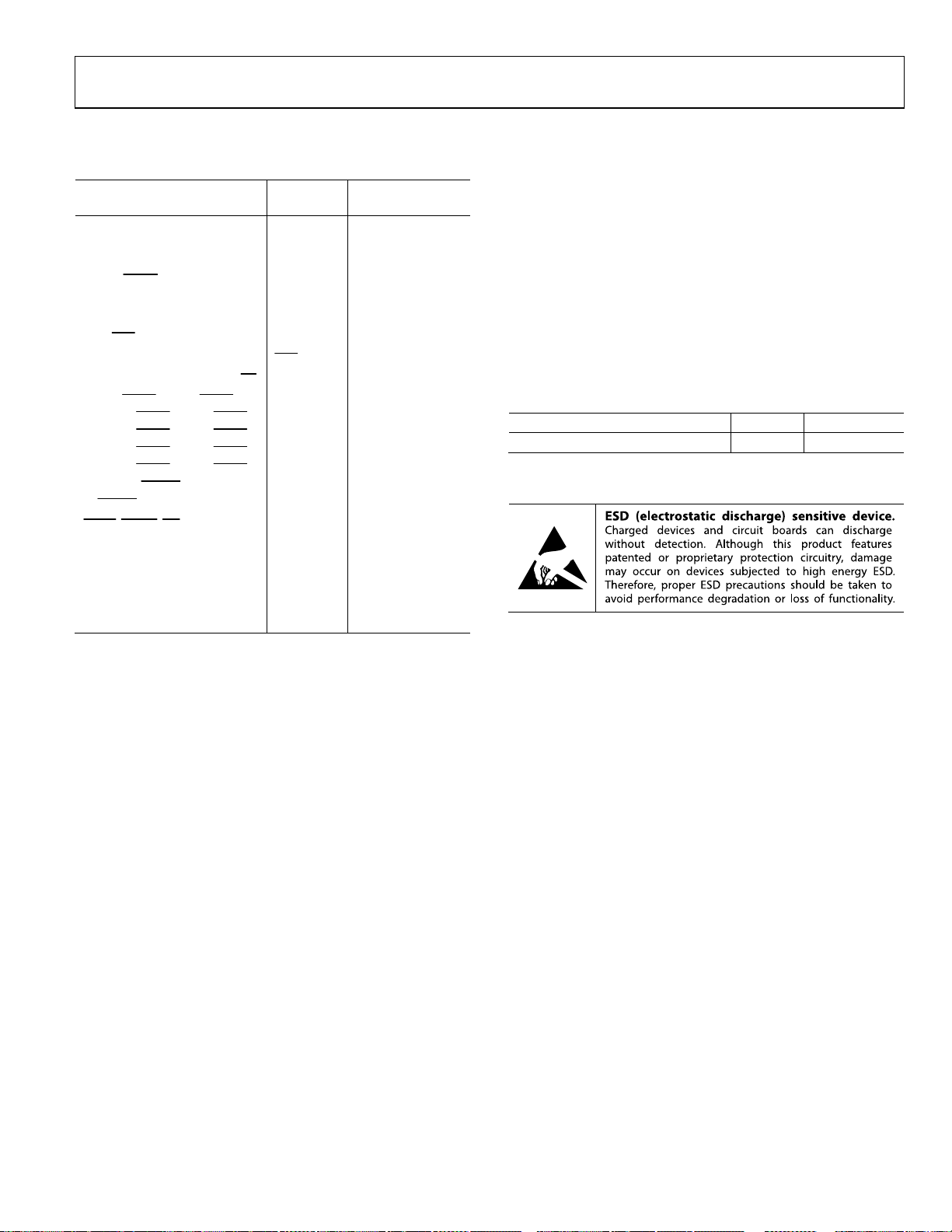
ABSOLUTE MAXIMUM RATINGS
Table 19.
With
Parameter or Pin
Respect to Rating
VS GND −0.3 V to +3.6 V
VCP, CP GND −0.3 V to +5.8 V
VS_DRV GND −0.3 V to +3.6 V
REFIN, REFIN
GND
−0.3 V to VS + 0.3 V
RSET, LF, BYPASS GND −0.3 V to VS + 0.3 V
CPRSET GND −0.3 V to VS + 0.3 V
CLK, CLK
CLK
SCLK/SCL, SDIO/SDA, SDO, CS
OUT0, OUT0, OUT1, OUT1,
OUT2, OUT2
OUT4, OUT4
, OUT3, OUT3,
, OUT5, OUT5,
GND
CLK
GND
GND
−0.3 V to VS + 0.3 V
−1.2 V to +1.2 V
−0.3 V to VS + 0.3 V
−0.3 V to VS + 0.3 V
OUT6, OUT6, OUT7, OUT7,
OUT8, OUT8, OUT9, OUT9,
OUT10, OUT10
OUT11
SYNC, RESET, PD
, OUT11,
GND −0.3 V to VS + 0.3 V
REFMON, STATUS, LD GND −0.3 V to VS + 0.3 V
SP0, SP1, EEPROM GND −0.3 V to VS + 0.3 V
Junction Temperature
1
150°C
Storage Temperature Range −65°C to +150°C
Lead Temperature (10 sec) 300°C
1
See Table 20 for θJA.
Stresses above those listed under Absolute Maximum Ratings
may cause permanent damage to the device. This is a stress
rating only; functional operation of the device at these or any
other conditions above those indicated in the operational
section of this specification is not implied. Exposure to absolute
maximum rating conditions for extended periods may affect
device reliability.
THERMAL RESISTANCE
Thermal impedance measurements were taken on a JEDEC
JESD51-5 2S2P test board in still air in accordance with JEDEC
JESD51-2. See the Thermal Performance section for more details.
Table 20.
Package Type θJA Unit
64-Lead LFCSP (CP-64-4) 22 °C/W
ESD CAUTION
Rev. 0 | Page 17 of 84
AD9520-1
S
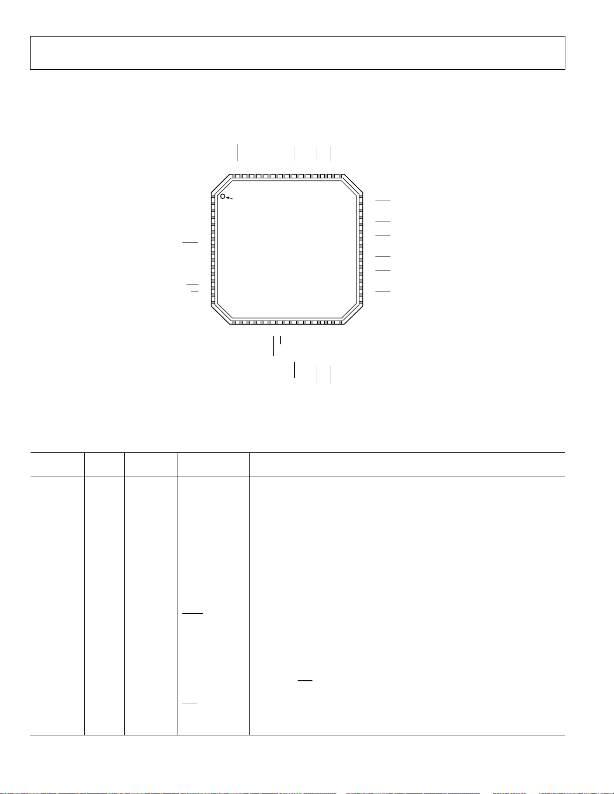
PIN CONFIGURATION AND FUNCTION DESCRIPTIONS
REFIN (REF 1)
REFIN (REF 2)
CPRSETVSVS
GND
RSETVSOUT0 (OUT0A)
OUT0 (OUT0B)
VS_DRV
OUT1 (OUT1A)
OUT1 (OUT1B)
OUT2 (OUT2A)
OUT2 (OUT2B)
646362616059585756555453525150
VS
49
VS
1
PIN 1
REFMON
LD
VCP
CP
STATUS
REF_SEL
SYNC
LF
BYPASS
10
VS
11
VS
12
CLK
13
CLK
14
CS
15
16
CLK/SCL
NOTES
1. EXPOSE D DIE PAD MUST BE CONNECTED TO GND.
INDICATO R
2
3
4
5
6
7
8
9
171819202122232425262728293031
SDIO/SDA
SDO
GND
AD9520
TOP VIEW
(Not to Scale)
SP1
SP0
EEPROM
PD
RESET
VS_DRV
OUT10A)
T9 (OUT9A)
T9 (OUT9B)
OU
OU
OUT10 (
OUT10B)
OUT10 (
OUT11A)
OUT11 (
OUT11B)
OUT11 (
32
VS
48
OUT3 (OUT3A)
47
OUT3 (OUT3B)
46
VS_DRV
45
OUT4 (OUT4A)
44
OUT4 (OUT4B)
43
OUT5 (OUT5A)
42
OUT5 (OUT5B)
41
VS
40
VS
39
OUT8 (OUT8B)
38
OUT8 (OUT8A)
37
OUT7 (OUT7B)
36
OUT7 (OUT7A)
35
VS_DRV
34
OUT6 (OUT6B)
33
OUT6 (OUT6A)
07214-003
Figure 5. Pin Configuration
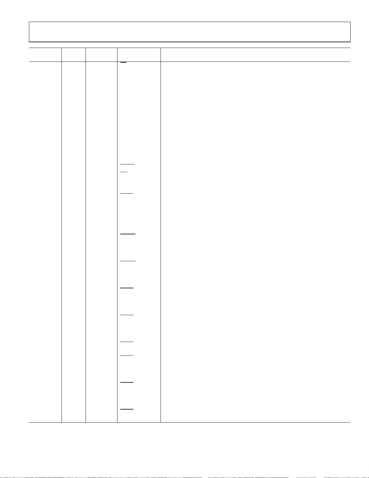
Table 21. Pin Function Descriptions
Pin No.
1, 11, 12, 32,
Input/
Output
I Power VS 3.3 V Power Pins.
Pin
Type Mnemonic Description
40, 41, 49,
57, 60, 61
2 O 3.3 V CMOS REFMON Reference Monitor (Output). This pin has multiple selectable outputs.
3 O 3.3 V CMOS LD
4 I Power VCP
Lock Detect (Output). This pin has multiple selectable outputs.
Power Supply for Charge Pump (CP); VS < VCP < 5.0 V. VCP must still be connected
to 3.3 V if the PLL is not used.
5 O Loop filter CP
Charge Pump (Output). This pin connects to an external loop filter. This pin can
be left unconnected if the PLL is not used.
6 O 3.3 V CMOS STATUS
7 I 3.3 V CMOS REF_SEL
Programmable Status Output.
Reference Select. It selects REF1 (low) or REF2 (high). This pin has an internal
30 kΩ pull-down resistor.
8 I 3.3 V CMOS
SYNC
Manual Synchronizations and Manual Holdover. This pin initiates a manual
synchronization and is used for manual holdover. Active low. This pin has an
internal 30 kΩ pull-up resistor.
9 I Loop filter LF
10 O Loop filter BYPASS
Loop Filter (Input). It connects internally to the VCO control voltage node.
This pin is for bypassing the LDO to ground with a 220 nF capacitor.
This pin can be left unconnected if the PLL is not used.
13 I
Differential
CLK
Along with CLK
, this pin is the differential input for the clock distribution section.
clock input
14 I
Differential
clock input
Along with CLK, this pin is the differential input for the clock distribution section. If a
CLK
single-ended input is connected to the CLK pin, connect a 0.1 μF bypass capacitor
from this pin to ground.
Rev. 0 | Page 18 of 84
AD9520-1
Input/
Pin No.
Output
15 I 3.3 V CMOS
16 I 3.3 V CMOS SCLK/SCL
17 I/O 3.3 V CMOS SDIO/SDA Serial Control Port Bidirectional Serial Data In/Out.
18 O 3.3 V CMOS SDO Serial Control Port Unidirectional Serial Data Out.
19, 59 I GND GND Ground Pins.
20 I
21 I
22 I 3.3 V CMOS EEPROM
23 I 3.3 V CMOS
24 I 3.3 V CMOS
25 O
26 O
27, 35,
I Power VS_DRV
46, 54
28 O
29 O
30 O
31 O
33 O
34 O
36 O
37 O
38 O
39 O
42 O
43 O
44 O
45 O
47 O
Pin
Type Mnemonic Description
Serial Control Port Chip Select; Active Low. This pin has an internal 30 kΩ
CS
pull-up resistor.
Serial Control Port Clock Signal. This pin has an internal 30 kΩ pull-down resistor
in SPI mode but is high impedance in I²C mode.
Three-level
logic
Three-level
logic
SP1
SP0
Select SPI or I²C as the serial interface port and select the I²C slave address in I²C
mode. Three-level logic. This pin is internally biased for the open logic level.
Select SPI or I²C as the serial interface port and select the I²C slave address in I²C
mode. Three-level logic. This pin is internally biased for the open logic level.
Setting this pin high selects the register values stored in the internal EEPROM to
be loaded at reset and/or power-up. Setting this pin low causes the AD9520 to
load the hard-coded default register values at power-up/reset. This pin has an
internal 30 kΩ pull-down resistor.
Chip Reset, Active Low. This pin has an internal 30 kΩ pull-up resistor.
Chip Power-Down, Active Low. This pin has an internal 30 kΩ pull-up resistor.
Clock Output. This pin can be configured as one side of a differential LVPECL
output or as a single-ended CMOS output.
output or as a single-ended CMOS output.
LVPECL or
CMOS
LVPECL or
CMOS
RESET
PD
OUT9 (OUT9A)
(OUT9B) Clock Output. This pin can be configured as one side of a differential LVPECL
OUT9
Output Driver Power Supply Pins. As a group, these pins can be set to either
2.5 V or 3.3 V. All four pins must be set to the same voltage.
LVPECL or
CMOS
LVPECL or
CMOS
LVPECL or
CMOS
LVPECL or
CMOS
LVPECL or
CMOS
LVPECL or
CMOS
LVPECL or
CMOS
LVPECL or
CMOS
LVPECL or
CMOS
LVPECL or
CMOS
LVPECL or
CMOS
LVPECL or
CMOS
LVPECL or
CMOS
LVPECL or
CMOS
LVPECL or
CMOS
OUT10 (OUT10A)
Clock Output. This pin can be configured as one side of a differential LVPECL
output or as a single-ended CMOS output.
(OUT10B) Clock Output. This pin can be configured as one side of a differential LVPECL
OUT10
output or as a single-ended CMOS output.
OUT11 (OUT11A)
Clock Output. This pin can be configured as one side of a differential LVPECL
output or as a single-ended CMOS output.
(OUT11B) Clock Output. This pin can be configured as one side of a differential LVPECL
OUT11
output or as a single-ended CMOS output.
OUT6 (OUT6A)
Clock Output. This pin can be configured as one side of a differential LVPECL
output or as a single-ended CMOS output.
(OUT6B) Clock Output. This pin can be configured as one side of a differential LVPECL
OUT6
output or as a single-ended CMOS output.
OUT7 (OUT7A)
Clock Output. This pin can be configured as one side of a differential LVPECL
output, or as a single-ended CMOS output.
(OUT7B) Clock Output. This pin can be configured as one side of a differential LVPECL
OUT7
output or as a single-ended CMOS output.
OUT8 (OUT8A)
Clock Output. This pin can be configured as one side of a differential LVPECL
output or as a single-ended CMOS output.
(OUT8B) Clock Output. This pin can be configured as one side of a differential LVPECL
OUT8
output or as a single-ended CMOS output.
(OUT5B) Clock Output. This pin can be configured as one side of a differential LVPECL
OUT5
output or as a single-ended CMOS output.
OUT5 (OUT5A)
Clock Output. This pin can be configured as one side of a differential LVPECL
output or as a single-ended CMOS output.
(OUT4B) Clock Output. This pin can be configured as one side of a differential LVPECL
OUT4
output or as a single-ended CMOS output.
OUT4 (OUT4A)
Clock Output. This pin can be configured as one side of a differential LVPECL
output or as a single-ended CMOS output.
(OUT3B) Clock Output. This pin can be configured as one side of a differential LVPECL
OUT3
output or as a single-ended CMOS output.
Rev. 0 | Page 19 of 84

AD9520-1
Input/
Pin No.
48 O
50 O
51 O
52 O
53 O
55 O
56 O
58 O
62 O
63 I
64 I
EPAD GND GND The exposed die pad must be connected to GND.
Output
Pin
Type Mnemonic Description
LVPECL or
CMOS
LVPECL or
CMOS
LVPECL or
CMOS
LVPECL or
CMOS
LVPECL or
CMOS
LVPECL or
CMOS
LVPECL or
CMOS
Current set
resistor
Current set
resistor
Reference
input
Reference
input
OUT3 (OUT3A)
(OUT2B) Clock Output. This pin can be configured as one side of a differential LVPECL
OUT2
OUT2 (OUT2A)
(OUT1B) Clock Output. This pin can be configured as one side of a differential LVPECL
OUT1
OUT1 (OUT1A)
(OUT0B) Clock Output. This pin can be configured as one side of a differential LVPECL
OUT0
OUT0 (OUT0A)
RSET
CPRSET
(REF2) Along with REFIN, this is the differential input for the PLL reference. Alternatively,
REFIN
REFIN (REF1)
Clock Output. This pin can be configured as one side of a differential LVPECL
output or as a single-ended CMOS output.
output or as a single-ended CMOS output.
Clock Output. This pin can be configured as one side of a differential LVPECL
output or as a single-ended CMOS output.
output or as a single-ended CMOS output.
Clock Output. This pin can be configured as one side of a differential LVPECL
output or as a single-ended CMOS output.
output or as a single-ended CMOS output.
Clock Output. This pin can be configured as one side of a differential LVPECL
output or as a single-ended CMOS output.
Clock Distribution Current Set Resistor. Connect a 4.12 kΩ resistor from this pin
to GND.
Charge Pump Current Set Resistor. Connect a 5.1 kΩ resistor from this pin to GND.
This resistor can be omitted if the PLL is not used.
this pin is a single-ended input for REF2.
Along with REFIN
this pin is a single-ended input for REF1.
, this is the differential input for the PLL reference. Alternatively,
Rev. 0 | Page 20 of 84
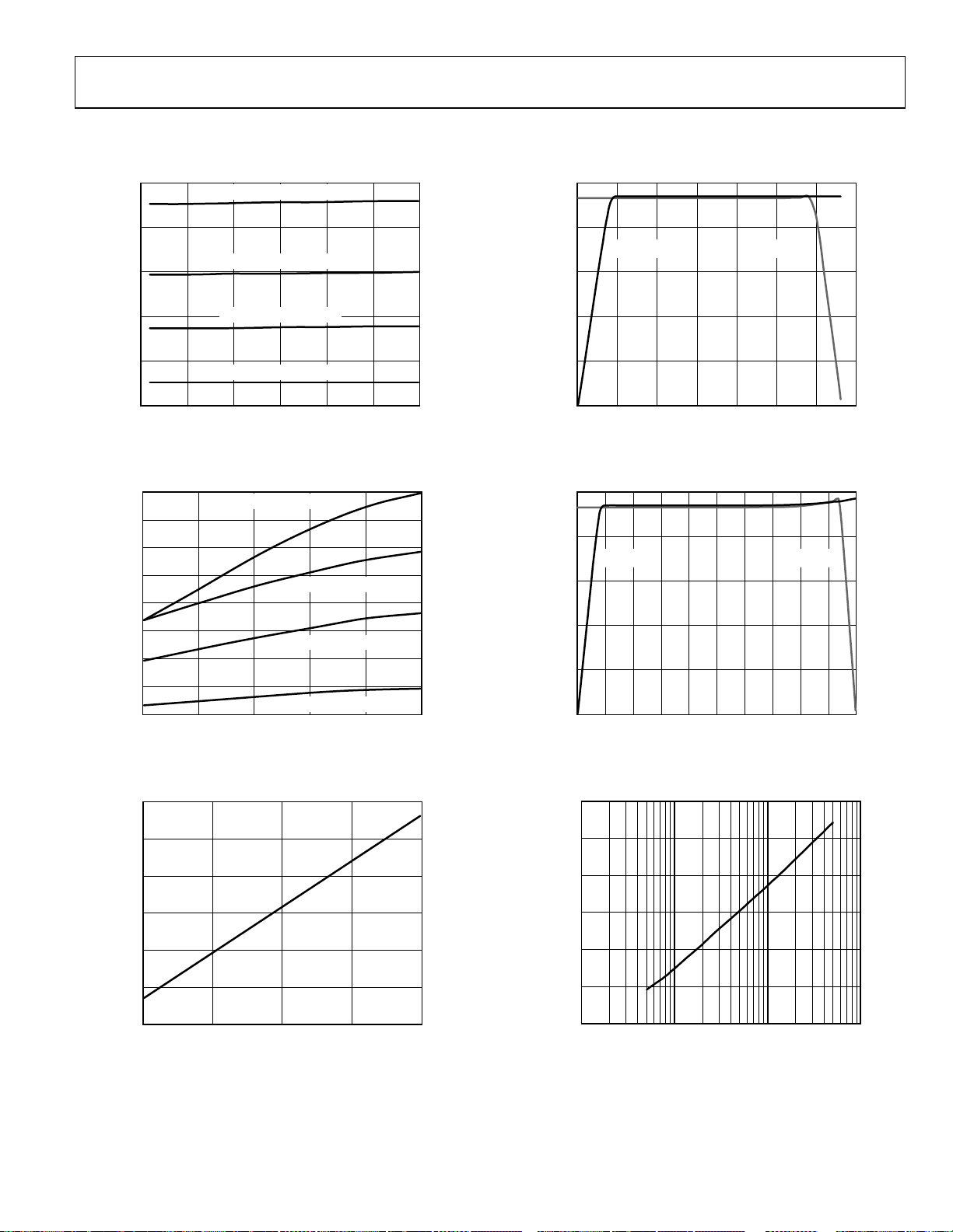
AD9520-1
–
TYPICAL PERFORMANCE CHARACTERISTICS
350
3 CHANNELS—6 LVPECL
5
300
250
200
CURRENT (mA)
150
100
0 500 1000 1500 2000 2500 3000
3 CHANNELS—3 LVPECL
2 CHANNELS—2 LVPECL
1 CHANNEL—1 LVPECL
FREQUENCY (MHz )
Figure 6. Total Current vs. Frequency, CLK-to-Output (PLL Off),
LVPECL Outputs Terminated 50 Ω to VS_DRV − 2 V
240
220
200
180
160
140
CURRENT (mA)
120
100
80
0 50 100 150 200 250
3 CHANNELS—6 CMOS
3 CHANNELS—3 CMOS
2 CHANNELS—2 CMOS
1 CHANNEL—1 CMOS
FREQUENCY (MHz)
Figure 7. Total Current vs. Frequency, CLK-to-Output (PLL Off),
CMOS Outputs with 10 pF Load
65
4
PUMP UPPUMP DOWN
3
2
CURRENT FROM CP P IN (mA)
1
0
033.02.52.01.51.00.5
07214-108
VOLTAGE ON CP PIN (V)
.5
07214-111
Figure 9. Charge Pump Characteristics @ VCP = 3.3 V
5
4
PUMP DOWN PUMP UP
3
2
CURRENT FROM CP P IN (mA)
1
0
054.03.0 4.53.52. 52.01.51.00.5
07214-109
VOLTAGE ON CP PIN (V)
.0
07214-112
Figure 10. Charge Pump Characteristics @ VCP = 5.0 V
140
60
55
50
(MHz/V)
VCO
K
45
40
35
2.3 2.72.62.52.4
VCO FREQUENCY (GHz)
Figure 8. K
VCO
07214-010
vs. VCO Frequency
–145
–150
–155
(dBc/Hz)
–160
–165
PFD PHASE NOI SE REFERRED TO PFD INPUT
–170
0.1 1 10010
PFD FREQUENCY (MHz)
Figure 11. PFD Phase Noise Referred to PFD Input vs. PFD Frequency
07214-013
Rev. 0 | Page 21 of 84
AD9520-1
–
208
–210
–212
–214
–216
–218
–220
PLL FIGURE OF MERIT (dBc/ Hz)
–222
–224
DIFFERENTIAL INPUT
SINGLE- ENDED INPUT
0 0.4 0.8 1.20.2 0.6 1.0 1.4
INPUT SLEW RATE (V/ns)
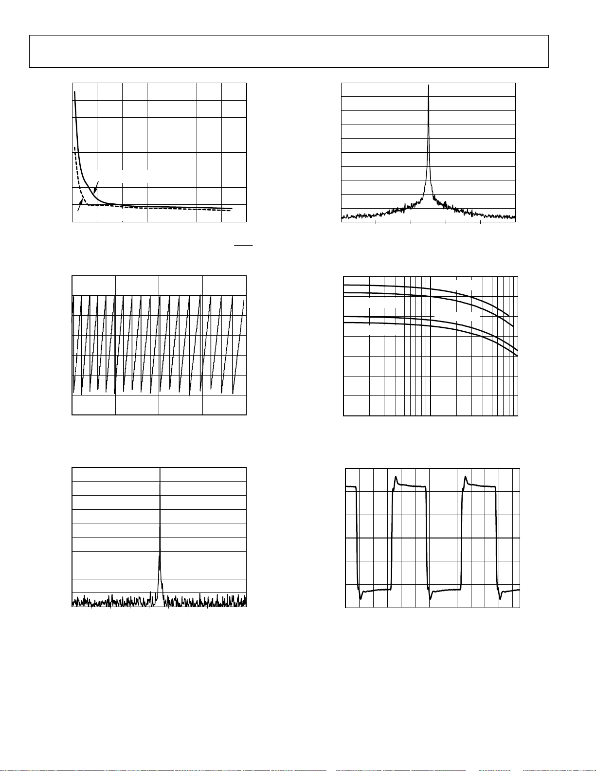
Figure 12. PLL Figure of Merit (FOM) vs. Slew Rate at REFIN/
1.9
1.8
1.7
1.6
1.5
REFIN
07214-114
0
–10
–20
–30
–40
–50
–60
POWER (dBm)
–70
–80
–90
–100
122.38 122.58 122. 78 122.98 123. 18 123.38
FREQUENCY (MHz )
Figure 15. Output Spectrum, LVPECL; 122.88 MHz; PFD = 15.36 MHz;
3.5
3.0
2.5
2.0
(V)
OH
V
1.5
LBW = 127 kHz; I
VS_DRV = 3.135V
VS_DRV = 2.35V
= 3.0 mA; f
CP
= 2458 MHz (new)
VCO
VS_DRV = 3.3V
VS_DRV = 2.5V
07214-117
1.4
VCO TUNING V OLTAGE (V)
1.3
1.2
2.3 2.4 2.5 2.6 2.7
FREQUENCY (GHz)
Figure 13. VCO Tuning Voltage vs. Frequency
0
–10
–20
–30
–40
–50
–60
POWER (dBm)
–70
–80
–90
–100
100 145140135130125120115110105
FREQUENCY (MHz)
Figure 14. PFD/CP Spurs; 122.88 MHz; PFD = 15.36 MHz;
LBW = 127 kHz; I
= 3.0 mA; f
CP
= 2458 MHz (new)
VCO
1.0
0.5
0
10k 1k 100
07214-115
Figure 16. CMOS Output VOH (Static) vs. R
RESISTIVE LOAD (Ω)
(to Ground)
LOAD
07214-118
1.2
0.8
0.4
0
–0.4
DIFFERENTIAL OUTPUT (V)
–0.8
–1.2
02222018161412108642
07214-116
TIME (ns)
4
07214-014
Figure 17. LVPECL Output (Differential) @ 100 MHz
Rev. 0 | Page 22 of 84
AD9520-1
–
1.0
2.0
0.6
0.2
–0.2
DIFFERENTIAL SWING (V p-p)
–0.6
–1.0
010.5 1.0
TIME (ns)
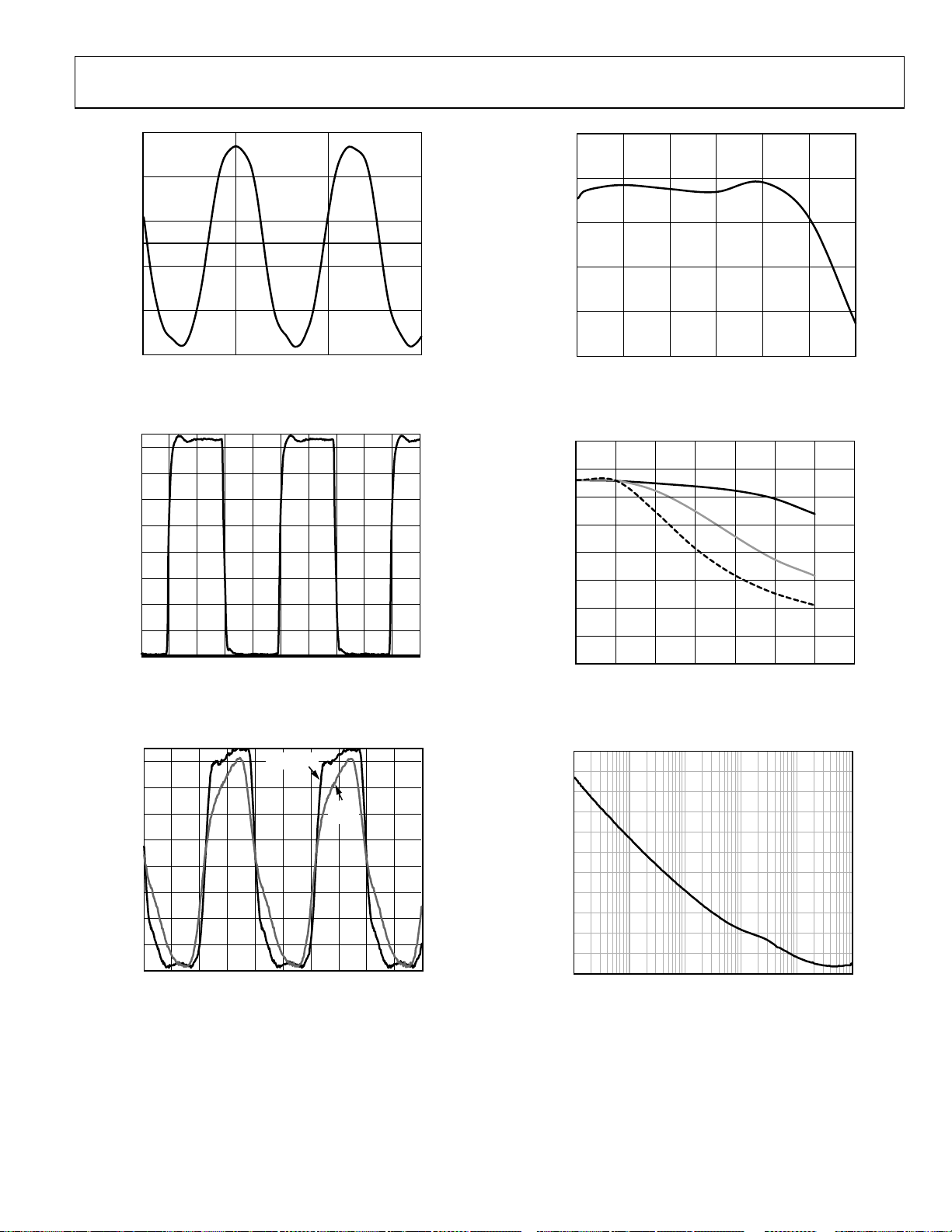
Figure 18. LVPECL Differential Voltage Swing @ 1600 MHz
.5
07214-015
1.8
1.6
1.4
DIFFERENTIAL SWING (V p-p)
1.2
1.0
031.5 2.0 2.51.00.5
Figure 21. LVPECL Differential Voltage Swing vs. Frequency
3.2
2.8
2.4
2.0
1.6
AMPLITUDE ( V)
1.2
0.8
0.4
0
0860 1004020 7050 903010
TIME (ns)
Figure 19. CMOS Output with 10 pF Load @ 25 MHz
0
07214-018
4.0
3.5
3.0
2.5
2.0
1.5
AMPLITUDE (V)
1.0
0.5
0
07
Figure 22. CMOS Output Swing vs. Frequency and Capacitive Load
3.2
2.8
2.4
2.0
1.6
AMPLITUDE (V)
1.2
0.8
0.4
0
010
2pF LOAD
TIME (ns)
10pF
LOAD
987654321
07214-019
Figure 20. CMOS Output with 2 pF and 10 pF Load @ 250 MHz
40
–50
–60
–70
–80
–90
–100
–110
PHASE NOISE (dBc/Hz)
–120
–130
–140
–150
1k 100M1M 10M100k10k
Figu re 23. Inter nal VC O Phas e Noise (Absolute), Direct-to-LVPECL @ 2300 MHz
FREQUENCY (GHz)
FREQUENCY (MHz )
FREQUENCY (Hz)
.0
07214-123
2pF
10pF
20pF
600500400300200100
00
07214-124
07214-023
Rev. 0 | Page 23 of 84
AD9520-1
–
–
–
–
–
–
40
–50
–60
–70
–80
–90
–100
–110
PHASE NOISE (dBc/Hz)
–120
–130
–140
–150
1k 100M1M 10M100k10k
FREQUENCY (Hz)
07214-024
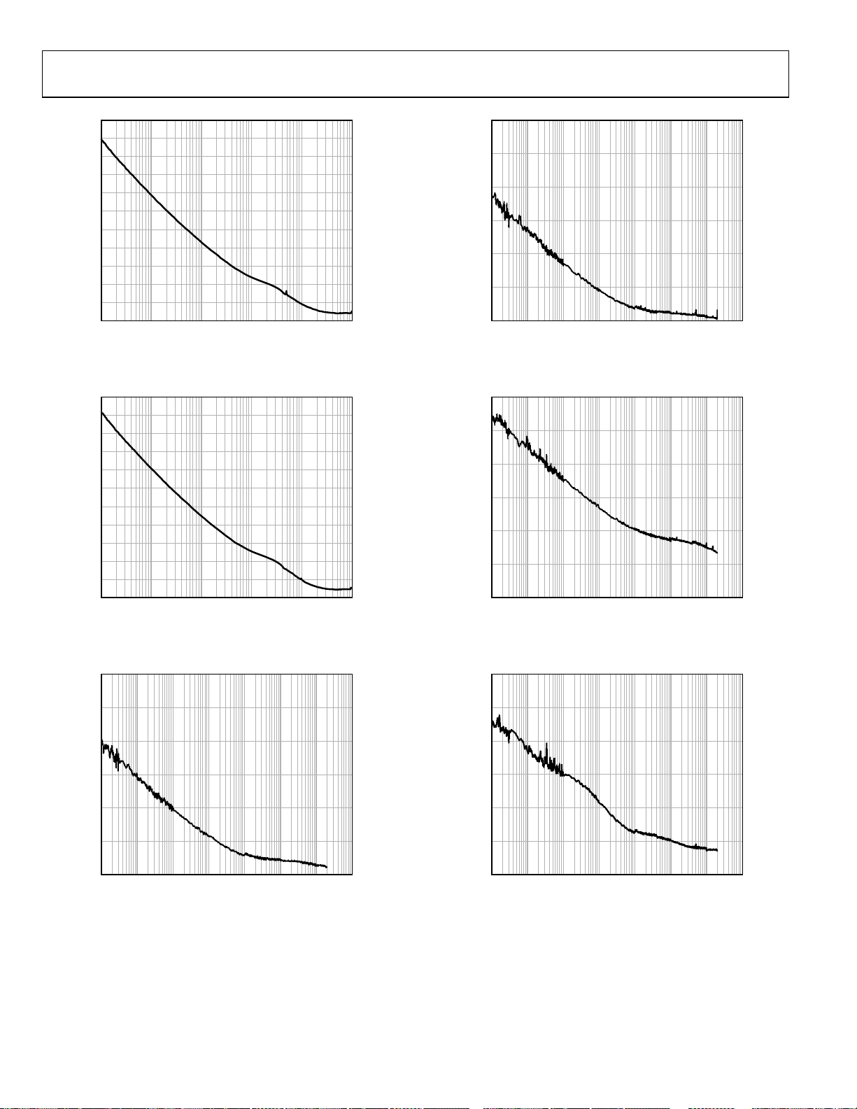
Figu re 24. In ternal VCO Phase No ise (Absolute), Direct-to-LVPECL @ 2475 MHz
40
–50
–60
–70
–80
–90
–100
–110
PHASE NOISE (dBc/Hz)
–120
–130
–140
–150
1k 100M1M 10M100k10k
FREQUENCY (Hz)
07214-025
Figu re 25. In ternal VCO Phase No ise (Absolute), Direct-to-LVPECL @ 2650 MHz
100
100
–110
–120
–130
–140
PHASE NOISE (dBc/Hz)
–150
–160
10 1k100 100M1M 10M100k10k
FREQUENCY (Hz)
Figure 27. Additive (Residual) Phase Noise, CLK-to-LVPECL @
200 MHz, Divide-by-5
100
–110
–120
–130
–140
PHASE NOISE (dBc/Hz)
–150
–160
10 1k100 100M1M 10M100k10k
FREQUENCY (Hz)
Figure 28. Additive (Residual) Phase Noise, CLK-to-LVPECL @
1600 MHz, Divide-by-1
110
07214-129
07214-130
–110
–120
–130
–140
PHASE NOISE (dBc/Hz)
–150
–160
10 1k100 100M1M 10M100k10k
FREQUENCY (Hz)
Figure 26. Additive (Residual) Phase Noise, CLK-to-LVPECL @
245.76 MHz, Divide-by-1
07214-128
–120
–130
–140
–150
PHASE NOISE (dBc/Hz)
–160
–170
10 1k100 100M1M 10M100k10k
FREQUENCY (Hz)
Figure 29. Additive (Residual) Phase Noise, CLK-to-CMOS @
50 MHz, Divide-by-20
07214-131
Rev. 0 | Page 24 of 84
AD9520-1
–
–
–
–
100
–110
–120
120
–130
–130
–140
PHASE NOISE (dBc/Hz)
–150
–160
10 1k100 100M1M 10M100k10k
FREQUENCY (Hz)
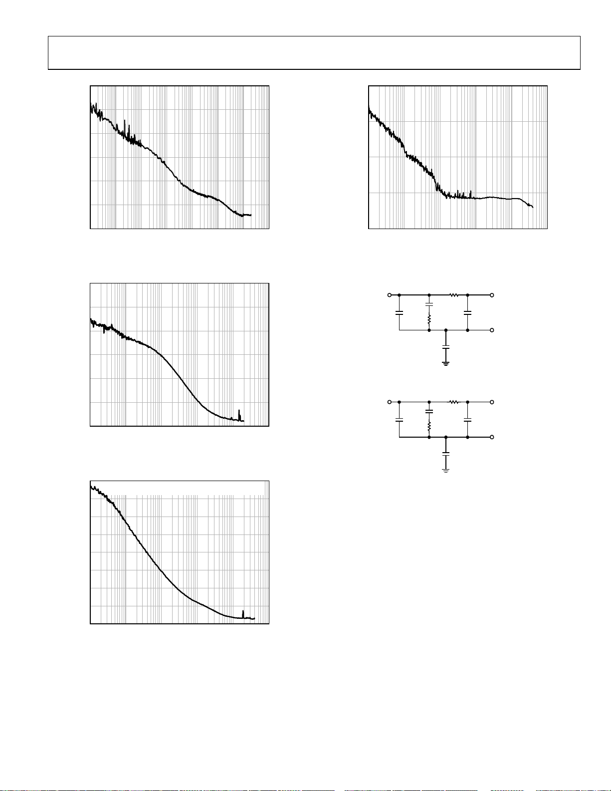
Figure 30. Additive (Residual) Phase Noise, CLK-to-CMOS @
250 MHz, Divide-by-4
100
–110
–120
–130
–140
PHASE NOISE (dBc/Hz)
–150
–160
1k 100M1M 10M100k10k
FREQUENCY (Hz)
Figure 31. Phase Noise (Absolute) Clock Generation; Internal VCO @
2.458 GHz; PFD = 15.36 MHz; LBW = 40 kHz; LVPECL Output = 122.88 MHz
80
INTEGRAT ED RMS JITTER (12kHz TO 20MHz): 582f s
–90
–100
–140
PHASE NOISE (dBc/Hz)
–150
–160
1k 100M1M 10M100k10k
07214-132
FREQUENCY (Hz)
07214-135
Figure 33. Phase Noise (Absolute), External VCXO (Toyocom TCO-2112)
@ 245.76 MHz; PFD = 15.36 MHz; LBW = 250 Hz; LVPECL Output = 245.76 MHz
R2
C2
62pF
BYPASS
CAPACITOR
FOR LDO
C1
240nF
R1
820Ω
390Ω
C12
220nF
C3
33pF
LFCP
BYPASS
07214-234
Figure 34. PLL Loop Filter Used for Clock Generation Plot (See Figure 31)
R2
3kΩ
C1
BYPASS
FOR LDO
4.7µF
R1
2.1kΩ
C12
220nF
C2
1.5nF
07214-033
CAPACITOR
C3
2.2nF
LFCP
BYPASS
07214-235
Figure 35. PLL Loop Filter Used for Clock Cleanup Plot (See Figure 32)
–110
–120
–130
PHASE NOISE (dBc/Hz)
–140
–150
–160
1k 100M1M 10M100k10k
FREQUENCY (Hz)
07214-034
Figure 32. Phase Noise (Absolute) Clock Cleanup; Internal VCO @ 2.488 GHz;
PFD = 120 kHz; LBW = 1.84 kHz; LVPECL Output = 155.52 MHz
Rev. 0 | Page 25 of 84

AD9520-1
TERMINOLOGY
Phase Jitter and Phase Noise
An ideal sine wave can be thought of as having a continuous
and even progression of phase with time from 0° to 360° for
each cycle. Actual signals, however, display a certain amount
of variation from ideal phase progression over time. This
phenomenon is called phase jitter. Although many causes can
contribute to phase jitter, one major cause is random noise,
which is characterized statistically as being Gaussian (normal)
in distribution.
This phase jitter leads to a spreading out of the energy of the
sine wave in the frequency domain, producing a continuous
power spectrum. This power spectrum is usually reported as a
series of values whose units are dBc/Hz at a given offset in
frequency from the sine wave (carrier). The value is a ratio
(expressed in decibels) of the power contained within a 1 Hz
bandwidth with respect to the power at the carrier frequency.
For each measurement, the offset from the carrier frequency is
also given.
It is meaningful to integrate the total power contained within
some interval of offset frequencies (for example, 10 kHz to
10 MHz). This is called the integrated phase noise over that
frequency offset interval and can be readily related to the time
jitter due to the phase noise within that offset frequency interval.
Phase noise has a detrimental effect on the performance of ADCs,
DACs, and RF mixers. It lowers the achievable dynamic range of
the converters and mixers, although they are affected in somewhat
different ways.
Time Jitter
Phase noise is a frequency domain phenomenon. In the time
domain, the same effect is exhibited as time jitter. When observing
a sine wave, the time of successive zero crossings varies. In a square
wave, the time jitter is a displacement of the edges from their
ideal (regular) times of occurrence. In both cases, the variations in
timing from the ideal are the time jitter. Because these variations
are random in nature, the time jitter is specified in seconds root
mean square (rms) or 1 sigma of the Gaussian distribution.
Time jitter that occurs on a sampling clock for a DAC or an
ADC decreases the signal-to-noise ratio (SNR) and dynamic
range of the converter. A sampling clock with the lowest possible
jitter provides the highest performance from a given converter.
Additive Phase Noise
Additive phase noise is the amount of phase noise that is
attributable to the device or subsystem being measured.
The phase noise of any external oscillators or clock sources is
subtracted. This makes it possible to predict the degree to which
the device impacts the total system phase noise when used in
conjunction with the various oscillators and clock sources, each
of which contributes its own phase noise to the total. In many
cases, the phase noise of one element dominates the system
phase noise. When there are multiple contributors to phase
noise, the total is the square root of the sum of squares of the
individual contributors.
Additive Time Jitter
Additive time jitter is the amount of time jitter that is attributable to
the device or subsystem being measured. The time jitter of any
external oscillators or clock sources is subtracted. This makes it
possible to predict the degree to which the device impacts the
total system time jitter when used in conjunction with the various
oscillators and clock sources, each of which contributes its own
time jitter to the total. In many cases, the time jitter of the external
oscillators and clock sources dominates the system time jitter.
Rev. 0 | Page 26 of 84
 Loading...