Integrated 2.5 GHz VCO
AD9518-1
Rev. C
Trademarks and registered trademarks are the property of their respective owners.
Fax: 781.461.3113 ©2007–2012 Analog Devices, Inc. All rights reserved.
REFIN
REF1
REF2
CLK
LF
SWITCHOVER
AND MONITOR
PLL
DIVIDER
AND MUXs
CP
VCO
STATUS
MONITOR
LVPECL
LVPECL
SERIAL CONTROL PORT
AND
DIGITAL LOGIC
AD9518-1
OUT0
OUT1
OUT2
OUT3
OUT4
OUT5
DIV/Φ
DIV/Φ
DIV/Φ
LVPECL
06430-001
Data Sheet
FEATURES
Low phase noise, phase-locked loop (PLL)
On-chip VCO tunes from 2.30 GHz to 2.65 GHz
External VCO/VCXO to 2.4 GHz optional
1 differential or 2 single-ended reference inputs
Reference monitoring capability
Automatic revertive and manual reference
switchover/holdover modes
Accepts LVPECL, LVDS, or CMOS references to 250 MHz
Programmable delays in path to PFD
Digital or analog lock detect, selectable
3 pairs of 1.6 GHz LVPECL outputs
Each output pair shares a 1-to-32 divider with coarse
phase delay
Additive output jitter: 225 fs rms
Channel-to-channel skew paired outputs of <10 ps
Automatic synchronization of all outputs on power-up
Manual output synchronization available
Available in a 48-lead LFCSP
APPLICATIONS
Low jitter, low phase noise clock distribution
10/40/100 Gb/sec networking line cards, including SONET,
Synchronous Ethernet, OTU2/3/4
Forward error correction (G.710)
Clocking high speed ADCs, DACs, DDSs, DDCs, DUCs, MxFEs
High performance wireless transceivers
ATE and high performance instrumentation
GENERAL DESCRIPTION
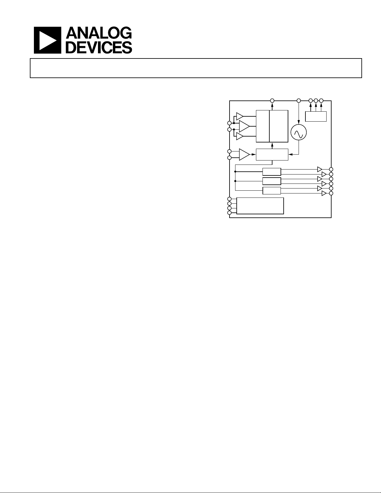
The AD9518-11 provides a multi-output clock distribution
function with subpicosecond jitter performance, along with an
on chip PLL and VCO. The on-chip VCO tunes from 2.30 GHz to
2.65 GHz. Optionally, an external VCO/VCXO of up to 2.4 GHz
can be used.
The AD9518-1 emphasizes low jitter and phase noise to maximize
data converter performance, and it can benefit other applications
with demanding phase noise and jitter requirements.
The AD9518-1 features six LVPECL outputs (in three pairs).
The LVPECL outputs operate to 1.6 GHz.
For applications that require additional outputs, a crystal
reference input, zero-delay, or EEPROM for automatic
configuration at startup, the AD9520 and AD9522 are available.
6-Output Clock Generator with
FUNCTIONAL BLOCK DIAGRAM
Figure 1.
In addition, the AD9516 and AD9517 are similar to the AD9518
but have a different combination of outputs.
Each pair of outputs has dividers that allow both the divide
ratio and coarse delay (or phase) to be set. The range of division
for the LVPECL outputs is 1 to 32.
The AD9518-1 is available in a 48-lead LFCSP and can be
operated from a single 3.3 V supply. An external VCO, which
requires an extended voltage range, can be accommodated by
connecting the charge pump supply (VCP) to 5 V. A separate
LVPECL power supply can be from 2.5 V to 3.3 V (nominal).
The AD9518-1 is specified for operation over the industrial
range of −40°C to +85°C.
1
AD9518 is used throughout the data sheet to refer to all the members of the
AD9518 family. However, when AD9518-1 is used, it refers to that specific
member of the AD9518 family.
Information furnishe d by Analog Devices is believed to be accurate and reliable. However, no
responsibility is assumed by Analog Devices for its use, nor for any infringements of patents or other
rights of third parties that may result from its use. Specifications subject to change without notice. No
license is granted by implication or otherwise under any patent or patent rights of Analog Devices.
One Technology Way, P.O. Box 9106, Norwood, MA 02062-9106, U.S.A.
Tel: 781.329.4700
www.analog.com

AD9518-1 Data Sheet
TABLE OF CONTENTS
Features .............................................................................................. 1
Applications ....................................................................................... 1
General Description ......................................................................... 1
Functional Block Diagram .............................................................. 1
Revision History ............................................................................... 3
Specifications ..................................................................................... 4
Power Supply Requirements ....................................................... 4
PLL Characteristics ...................................................................... 4
Clock Inputs .................................................................................. 6
Clock Outputs ............................................................................... 6
Timing Characteristics ................................................................ 6
Clock Output Additive Phase Noise (Distribution Only;
VCO Divider Not Used) .............................................................. 7
Clock Output Absolute Phase Noise (Internal VCO Used) .... 7
Clock Output Absolute Time Jitter (Clock Generation
Using Internal VCO) .................................................................... 8
Clock Output Absolute Time Jitter (Clock Cleanup Using
Internal VCO) ............................................................................... 8
Clock Output Absolute Time Jitter (Clock Generation
Using External VCXO) ................................................................ 8
Clock Output Additive Time Jitter (VCO Divider
Not Used) ....................................................................................... 9
Clock Output Additive Time Jitter (VCO Divider Used) ....... 9
Serial Control Port ..................................................................... 10
PD, SYNC
LD, STATUS, and REFMON Pins ............................................ 11
Power Dissipation ....................................................................... 11
Timing Diagrams ............................................................................ 12
Absolute Maximum Ratings .......................................................... 13
, and
RESET
Pins ..................................................... 10
Thermal Resistance .................................................................... 13
ESD Caution................................................................................ 13
Pin Configuration and Function Descriptions ........................... 14
Typical Performance Characteristics ........................................... 16
Terminology .................................................................................... 20
Detailed Block Diagram ................................................................ 21
Theory of Operation ...................................................................... 22
Operational Configurations ...................................................... 22
Digital Lock Detect (DLD) ....................................................... 30
Clock Distribution ..................................................................... 34
Reset Modes ................................................................................ 38
Power-Down Modes .................................................................. 38
Serial Control Port ......................................................................... 40
Serial Control Port Pin Descriptions ....................................... 40
General Operation of Serial Control Port ............................... 40
The Instruction Word (16 Bits) ................................................ 41
MSB/LSB First Transfers ........................................................... 41
Thermal Performance .................................................................... 44
Control Registers ............................................................................ 45
Control Register Map Overview .............................................. 45
Control Register Map Descriptions ......................................... 47
Applications Information .............................................................. 59
Frequency Planning Using the AD9518 .................................. 59
Using the AD9518 Outputs for ADC Clock Applications .... 59
LVPECL Clock Distribution ..................................................... 60
Outline Dimensions ....................................................................... 61
Ordering Guide .......................................................................... 61
Rev. C | Page 2 of 64

Data Sheet AD9518-1
REVISION HISTORY
1/12—Rev. B to Rev. C
Change to 0x232 Description, Table 49 ........................................ 58
9/11—Rev. A to Rev. B
Changes to Applications and General Description Sections ....... 1
Change to CPRSET Pin Resistor Parameter, Table 1 .................... 4
Changes to Table 2 ............................................................................ 4
Change to Test Conditions/Comments Column of Output
Differential Voltage (V
) Parameter, Table 4 ............................... 5
OD
Change to Logic 1 Current and Logic 0 Current Parameters,
Tabl e 14 ............................................................................................. 10
Change to Test Conditions/Comments Column of LVPECL
Channel (Divider Plus Output Driver) Parameter, Table 16 ..... 11
Changes to Table 19 ........................................................................ 14
Changes to Captions, Figure 11 and Figure 16............................ 17
Added Figure 26, Renumbered Sequentially ............................... 19
Change to PLL External Loop Filter Section ............................... 27
Changes to Reference Switchover and Prescaler Sections ......... 28
Changes to Comments/Conditions Column, Table 27 .............. 29
Changes to Automatic/Internal Holdover Mode and
Frequency Status Monitors Sections ............................................. 32
Changes to VCO Calibration Section ........................................... 33
Changes to Clock Distribution Section ........................................ 34
Change to Write Section ................................................................. 40
Change to Figure 47 ........................................................................ 42
Changes to Table 41 ........................................................................ 44
Changes to Register Address 0x01C, Table 42 ............................ 45
Changes to Register Address 0x017, Bits[1:0] and
Register Address 0x018, Bits[2:0], Table 44 ................................. 50
Changes to Register Address 0x01C, Bits[5:1], Table 44 ............ 53
Change to Bit 5, Register Address 0x191, Register
Address 0x194, and Register Address 0x197, Table 46 ............... 56
Changes to LVPECL Clock Distribution Section ....................... 60
Updated Outline Dimensions and Changes to
Ordering Guide ............................................................................... 61
1/10—Rev. 0 to Rev. A
Added 48-Lead LFCSP Package (CP-48-8) .................... Universal
Changes to Features, Applications, and General Description ..... 1
Change to CPRSET Pin Resistor Parameter .................................. 4
Changes to V
Supply Parameter................................................. 11
CP
Changes to Table 18 ........................................................................ 13
Added Exposed Paddle Notation to Figure 4;
Changes to Table 19 ........................................................................ 14
Change to High Frequency Clock Distribution—CLK or
External VCO > 1600 MHz Section; Change to Table 21 .......... 22
Changes to Table 23 ........................................................................ 24
Change to Configuration and Register Settings Section ........... 25
Change to Phase Frequency Detector (PFD) Section ................ 26
Changes to Charge Pump (CP), On-Chip VCO, PLL
External Loop Filter, and PLL Reference Inputs Sections ......... 27
Change to Figure 31; Added Figure 32 ......................................... 27
Changes to Reference Switchover and Prescaler Sections ......... 28
Changes to A and B Counters Section and Table 27 .................. 29
Change to Holdover Section .......................................................... 31
Changes to VCO Calibration Section ........................................... 33
Changes to Clock Distribution Section ........................................ 34
Change to Table 32; Change to Channel Frequency
Division (0, 1, and 2) Section ........................................................ 35
Change to Write Section ................................................................ 40
Change to Figure 46 ........................................................................ 42
Added Thermal Performance Section; Added Table 41 ............ 44
Changes to 0x003 Register Address .............................................. 45
Changes to Table 43 ........................................................................ 47
Changes to Table 44 ........................................................................ 48
Changes to Table 45 ........................................................................ 55
Changes to Table 46 ........................................................................ 57
Changes to Table 47 ........................................................................ 58
Changes to Table 48 ........................................................................ 59
Added Frequency Planning Using the AD9518 Section ............ 60
Changes to LVDS Clock Distribution Section ............................ 61
Changes to Figure 52 and Figure 54; Added Figure 53 .............. 61
Added Exposed Paddle Notation to Outline Dimensions;
Changes to Ordering Guide ........................................................... 62
9/07—Revision 0: Initial Version
Rev. C | Page 3 of 64

AD9518-1 Data Sheet
REFERENCE INPUTS
Input Sensitivity
250 mV p-p
PLL figure of merit (FOM) increases with increasing slew rate
SPECIFICATIONS
Typical values are given for VS = V
Minimum and maximum values are given over full V
POWER SUPPLY REQUIREMENTS
Table 1.
Parameter Min Typ Max Unit Test Conditions/Comments
VS 3.135 3.3 3.465 V 3.3 V ± 5%
V
2.375 VS V Nominally 2.5 V to 3.3 V ± 5%
S_LVPE CL
VCP VS 5.25 V Nominally 3.3 V to 5.0 V ± 5%
RSET Pin Resistor 4.12 kΩ Sets internal biasing currents; connect to ground
CPRSET Pin Resistor 2.7 5.1 10 kΩ Sets internal CP current range, nominally 4.8 mA (CP_lsb = 600 µA);
BYPASS Pin Capacitor 220 nF Bypass for internal LDO regulator; necessary for LDO stability;
PLL CHARACTERISTICS
Table 2.
Parameter Min Typ Max Unit Test Conditions/Comments
VCO (ON-CHIP)
Frequency Range 2300 2650 MHz See Figure 11
VCO Gain (K
Tuning Voltage (VT) 0.5 VCP − 0.5 V VCP ≤ VS when using internal VCO; outside of this range, the CP
Frequency Pushing (Open-Loop) 1 MHz/V
Phase Noise at 100 kHz Offset −105 dBc/Hz f = 2475 MHz
Phase Noise at 1 MHz Offset −124 dBc/Hz f = 2475 MHz
) 50 MHz/V See Figure 6
VCO
= 3.3 V ± 5%; VS ≤ VCP ≤ 5.25 V; TA = 25°C; R
S_ LVPE CL
and TA (−40°C to +85°C) variation.
S
= 4.12 kΩ; CP
SET
= 5.1 kΩ, unless otherwise noted.
RSET
actual current can be calculated by CP_lsb = 3.06/CPRSET;
connect to ground
connect to ground
spurs may increase due to CP up/down mismatch
Differential Mode (REFIN,
REFIN
)
Differential mode (can accommodate single-ended input by
Input Frequency 0 250 MHz Frequencies below about 1 MHz should be dc-coupled; be careful
Self-Bias Voltage, REFIN 1.35 1.60 1.75 V Self-bias voltage of REFIN1
Self-Bias Voltage,
REFIN
1.30 1.50 1.60 V
Input Resistance, REFIN 4.0 4.8 5.9 kΩ
Input Resistance,
REFIN
4.4 5.3 6.4 kΩ
Dual Single-Ended Mode (REF1, REF2) Two single-ended CMOS-compatible inputs
Input Frequency (AC-Coupled) 20 250 MHz Slew rate > 50 V/µs
Input Frequency (DC-Coupled) 0 250 MHz Slew rate > 50 V/µs; CMOS levels
Input Sensitivity (AC-Coupled) 0.8 V p-p Should not exceed VS p-p
Input Logic High 2.0 V
Input Logic Low 0.8 V
Input Current −100 +100 µA
Pulse Width High/Low 1.8 ns This value determines the allowable input duty cycle and is the
Input Capacitance 2 pF
PHASE/FREQUENCY DETECTOR (PFD)
PFD Input Frequency 100 MHz Antibacklash pulse width = 1.3 ns, 2.9 ns
45 MHz Antibacklash pulse width = 6.0 ns
Antibacklash Pulse Width 1.3 ns Register 0x017[1:0] = 01b
2.9 ns Register 0x017[1:0] = 00b; Register 0x017[1:0] = 11b
6.0 ns Register 0x017[1:0] = 10b
Rev. C | Page 4 of 64
ac grounding undriven input)
to match V
(self-bias voltage)
CM
(see Figure 10); the input sensitivity is sufficient for ac-coupled
LVPECL and LVDS signals
Self-bias voltage of
Self-biased
Self-biased
1
1
REFIN
1
amount of time that a square wave is high/low
Each pin, REFIN/
REFIN
(REF1/REF2)

Data Sheet AD9518-1
Sink-and-Source Current Matching
2 % 0.5 < CPV < VCP − 0.5 V
P = 1 FD
300
MHz
P = 2 DM (2/3)
200
MHz
Prescaler Output Frequency
300
MHz
A, B counter input frequency (prescaler input frequency divided
110
880 ps
At 50 MHz PFD Frequency
−143 dBc/Hz
High Range (ABP 1.3 ns, 2.9 ns)
7.5 ns
Register 0x017[1:0] = 00b, 01b, 11b; Register 0x018[4] = 0b
High Range (ABP 1.3 ns, 2.9 ns)
15 ns
Register 0x017[1:0] = 00b, 01b, 11b; Register 0x018[4] = 0b
Parameter Min Typ Max Unit Test Conditions/Comments
CHARGE PUMP (CP) CPV is CP pin voltage; VCP is charge pump power supply voltage
ICP Sink/Source Programmable
High Value 4.8 mA With CP
Low Value 0.60 mA
Absolute Accuracy 2.5 % CPV = VCP/2 V
CP
Range 2.7/10 kΩ
RSET
ICP High Impedance Mode Leakage 1 nA
ICP vs. CPV 1.5 % 0.5 < CPV < VCP − 0.5 V
ICP vs. Temperature 2 % CPV = VCP/2 V
PRESCALER (PART OF N DIVIDER)
See the
Prescaler Input Frequency
P = 2 FD 600 MHz
P = 3 FD 900 MHz
P = 4 DM (4/5) 1000 MHz
P = 8 DM (8/9) 2400 MHz
P = 16 DM (16/17) 3000 MHz
P = 32 DM (32/33) 3000 MHz
by P)
PLL DIVIDER DELAYS Register 0x019: R, Bits[5:3]; N, Bits[2:0] (see Table 44)
000 Off ps
001 330 ps
010 440 ps
011 550 ps
100 660 ps
101 770 ps
= 5.1 kΩ
RSET
VCXO/VCO Feedback Divider N—P, A, B, R section
111 990 ps
NOISE CHARACTERISTICS
In-Band Phase Noise of the Charge
Pump/Phase Frequency Detector
(In-Band Is Within the LBW of the PLL)
The PLL in-band phase noise floor is estimated by measuring the
in-band phase noise at the output of the VCO and subtracting
20 log(N) (where N is the value of the N divider)
At 500 kHz PFD Frequency −165 dBc/Hz
At 1 MHz PFD Frequency −162 dBc/Hz
At 10 MHz PFD Frequency −151 dBc/Hz
PLL Figure of Merit (FOM) −220 dBc/Hz Reference slew rate > 0.25 V/ns; FOM + 10 log(f
PFD
mation of the PFD/CP in-band phase noise (in the flat region) inside
the PLL loop bandwidth; when running closed-loop, the phase
noise, as observed at the VCO output, is increased by 20 log(N)
PLL DIGITAL LOCK DETECT WINDOW2 Signal available at LD, STATUS, and REFMON pins
when selected by appropriate register settings
Required to Lock (Coincidence of Edges) Selected by Register 0x017[1:0] and Register 0x018[4]
Low Range (ABP 1.3 ns, 2.9 ns) 3.5 ns Register 0x017[1:0] = 00b, 01b,11b; Register 0x018[4] = 1b
High Range (ABP 6.0 ns) 3.5 ns Register 0x017[1:0] = 10b; Register 0x018[4] = 0b
To Unlock After Lock (Hysteresis)2
Low Range (ABP 1.3 ns, 2.9 ns) 7 ns Register 0x017[1:0] = 00b, 01b, 11b; Register 0x018[4] = 1b
High Range (ABP 6.0 ns) 11 ns Register 0x017[1:0] = 10b; Register 0x018[4] = 0b
1
REFIN and
2
For reliable operation of the digital lock detect, the period of the PFD frequency must be greater than the unlock-after-lock time.
REFIN
self-bias points are offset slightly to avoid chatter on an open input condition.
) is an approxi-
Rev. C | Page 5 of 64

AD9518-1 Data Sheet
CLOCK INPUTS (CLK,
)
Differential input
Input Capacitance
2
pF
V
−
V
−
V
−
CLOCK INPUTS
Table 3.
Parameter Min Typ Max Unit Test Conditions/Comments
CLK
Input Frequency 01 2.4 GHz High frequency distribution (VCO divider)
01 1.6 GHz Distribution only (VCO divider bypassed)
Input Sensitivity, Differential 150 mV p-p Measured at 2.4 GHz; jitter performance is
improved with slew rates > 1 V/ns
Input Level, Differential 2 V p-p Larger voltage swings may turn on the protection
diodes and may degrade jitter performance
Input Common-Mode Voltage, VCM 1.3 1.57 1.8 V Self-biased; enables ac coupling
Input Common-Mode Range, V
Input Sensitivity, Single-Ended 150 mV p-p CLK ac-coupled;
Input Resistance 3.9 4.7 5.7 kΩ Self-biased
1
Below about 1 MHz, the input should be dc-coupled. Care should be taken to match VCM.
CLOCK OUTPUTS
Table 4.
Parameter Min Typ Max Unit Test Conditions/Comments
LVPECL CLOCK OUTPUTS Termination = 50 Ω to VS − 2 V
OUT0, OUT1, OUT2, OUT3, OUT4, OUT5 Differential (OUT,
Output Frequency, Maximum 2950 MHz Using direct to output; see Figure 16 for peak-to-peak
Output High Voltage (VOH)
Output Low Voltage (VOL)
Output Differential Voltage (VOD) 550 790 980 mV
1.3 1.8 V With 200 mV p-p signal applied; dc-coupled
CMR
ac-bypassed to RF ground
CLK
)
OUT
V
S_LVPECL
1.12
S_LVPECL
2.03
−
V
S_LVPECL
0.98
S_LVPECL
1.77
−
V
S_LVPECL
0.84
S_LVPECL
1.49
−
V
V
differential amplitude
This is VOH − VOL for each leg of a differential pair for
default amplitude setting with driver not toggling; the
peak-to-peak amplitude measured using a differential
probe across the differential pair with the driver toggling
is roughly 2× these values (see Figure 16
over frequency)
for variation
TIMING CHARACTERISTICS
Table 5.
Parameter Min Typ Max Unit Test Conditions/Comments
LVPECL Termination = 50 Ω to VS − 2 V; level = 810 mV
Output Rise Time, tRP 70 180 ps 20% to 80%, measured differentially
Output Fall Time, tFP 70 180 ps 80% to 20%, measured differentially
PROPAGATION DELAY, t
OUTPUT
High Frequency Clock Distribution
Configuration
Clock Distribution Configuration 773 933 1090 ps See Figure 30
Variation with Temperature 0.8 ps/°C
OUTPUT SKEW, LVPECL OUTPUTS1
LVPECL Outputs That Share the Same
Divider
LVPECL Outputs on Different Dividers 13 40 ps
All LVPECL Outputs Across Multiple Parts 220 ps
1
This is the difference between any two similar delay paths while operating at the same voltage and temperature.
, CLK-TO-LVPECL
PECL
835 995 1180 ps See Figure 28
5 15 ps
Rev. C | Page 6 of 64

Data Sheet AD9518-1
CLK-TO-LVPECL ADDITIVE PHASE NOISE
Distribution section only; does not include
At 100 MHz Offset
−149
dBc/Hz
VCO = 2.3 GHz; Output = 2.3 GHz
CLOCK OUTPUT ADDITIVE PHASE NOISE (DISTRIBUTION ONLY; VCO DIVIDER NOT USED)
Table 6.
Parameter Min Typ Max Unit Test Conditions/Comments
PLL and VCO
CLK = 1 GHz, Output = 1 GHz Input slew rate > 1 V/ns
Divider = 1
At 10 Hz Offset −109 dBc/Hz
At 100 Hz Offset −118 dBc/Hz
At 1 kHz Offset −130 dBc/Hz
At 10 kHz Offset −139 dBc/Hz
At 100 kHz Offset −144 dBc/Hz
At 1 MHz Offset −146 dBc/Hz
At 10 MHz Offset −147 dBc/Hz
CLK = 1 GHz, Output = 200 MHz Input slew rate > 1 V/ns
Divider = 5
At 10 Hz Offset −120 dBc/Hz
At 100 Hz Offset −126 dBc/Hz
At 1 kHz Offset −139 dBc/Hz
At 10 kHz Offset −150 dBc/Hz
At 100 kHz Offset −155 dBc/Hz
At 1 MHz Offset −157 dBc/Hz
>10 MHz Offset −157 dBc/Hz
CLOCK OUTPUT ABSOLUTE PHASE NOISE (INTERNAL VCO USED)
Table 7.
Parameter Min Typ Max Unit Test Conditions/Comments
LVPECL ABSOLUTE PHASE NOISE Internal VCO; direct to LVPECL output
VCO = 2.65 GHz; Output = 2.65 GHz
At 1 kHz Offset −46 dBc/Hz
At 10 kHz Offset −76 dBc/Hz
At 100 kHz Offset −104 dBc/Hz
At 1 MHz Offset −123 dBc/Hz
At 10 MHz Offset −140 dBc/Hz
At 40 MHz Offset −146 dBc/Hz
VCO = 2.475 GHz; Output = 2.475 GHz
At 1 kHz Offset −47 dBc/Hz
At 10 kHz Offset −77 dBc/Hz
At 100 kHz Offset −105 dBc/Hz
At 1 MHz Offset −124 dBc/Hz
At 10 MHz Offset −141 dBc/Hz
At 40 MHz Offset −146 dBc/Hz
At 1 kHz Offset −54 dBc/Hz
At 10 kHz Offset −78 dBc/Hz
At 100 kHz Offset −106 dBc/Hz
At 1 MHz Offset −125 dBc/Hz
At 10 MHz Offset −141 dBc/Hz
At 40 MHz Offset −146 dBc/Hz
Rev. C | Page 7 of 64

AD9518-1 Data Sheet
LVPECL OUTPUT ABSOLUTE TIME JITTER
Application example based on a typical
77 fs rms
Integration BW = 200 kHz to 10 MHz
CLOCK OUTPUT ABSOLUTE TIME JITTER (CLOCK GENERATION USING INTERNAL VCO)
Table 8.
Parameter Min Ty p Max Unit Test Conditions/Comments
setup where the reference source is clean,
so a wider PLL loop bandwidth is used;
reference = 15.36 MHz; R = 1
VCO = 2.46 GHz; LVPECL = 491.52 MHz; PLL LBW = 55 kHz 142 fs rms Integration BW = 200 kHz to 10 MHz
370 fs rms Integration BW = 12 kHz to 20 MHz
VCO = 2.46 GHz; LVPECL = 122.88 MHz; PLL LBW = 55 kHz 145 fs rms Integration BW = 200 kHz to 10 MHz
356 fs rms Integration BW = 12 kHz to 20 MHz
VCO = 2.46 GHz; LVPECL = 61.44 MHz; PLL LBW = 55 kHz 195 fs rms Integration BW = 200 kHz to 10 MHz
402 fs rms Integration BW = 12 kHz to 20 MHz
CLOCK OUTPUT ABSOLUTE TIME JITTER (CLOCK CLEANUP USING INTERNAL VCO)
Table 9.
Parameter Min Ty p Max Unit Test Conditions/Comments
LVPECL OUTPUT ABSOLUTE TIME JITTER Application example based on a typical
setup where the reference source is jittery,
so a narrower PLL loop bandwidth is used;
reference = 10.0 MHz; R = 20
VCO = 2.49 GHz; LVPECL = 622.08 MHz; PLL LBW = 125 Hz 745 fs rms Integration BW = 12 kHz to 20 MHz
VCO = 2.49 GHz; LVPECL = 155.52 MHz; PLL LBW = 125 Hz 712 fs rms Integration BW = 12 kHz to 20 MHz
VCO = 2.46 GHz; LVPECL = 122.88 MHz; PLL LBW = 125 Hz 700 fs rms Integration BW = 12 kHz to 20 MHz
CLOCK OUTPUT ABSOLUTE TIME JITTER (CLOCK GENERATION USING EXTERNAL VCXO)
Table 10.
Parameter Min Ty p Max Unit Test Conditions/Comments
LVPECL OUTPUT ABSOLUTE TIME JITTER Application example based on a typical
setup using an external 245.76 MHz VCXO
(Toyocom TCO-2112); reference = 15.36 MHz;
R = 1
LVPECL = 245.76 MHz; PLL LBW = 125 Hz 54 fs rms Integration BW = 200 kHz to 5 MHz
109 fs rms Integration BW = 12 kHz to 20 MHz
LVPECL = 122.88 MHz; PLL LBW = 125 Hz 79 fs rms Integration BW = 200 kHz to 5 MHz
114 fs rms Integration BW = 200 kHz to 10 MHz
163 fs rms Integration BW = 12 kHz to 20 MHz
LVPECL = 61.44 MHz; PLL LBW = 125 Hz 124 fs rms Integration BW = 200 kHz to 5 MHz
176 fs rms Integration BW = 200 kHz to 10 MHz
259 fs rms Integration BW = 12 kHz to 20 MHz
Rev. C | Page 8 of 64

Data Sheet AD9518-1
LVPECL OUTPUT ADDITIVE TIME JITTER
Distribution section only; does not include PLL and
CLOCK OUTPUT ADDITIVE TIME JITTER (VCO DIVIDER NOT USED)
Table 11.
Parameter Min Typ Max Unit Test Conditions/Comments
VCO; uses rising edge of clock signal
CLK = 622.08 MHz; LVPECL = 622.08 MHz;
Divider = 1
CLK = 622.08 MHz; LVPECL = 155.52 MHz;
Divider = 4
CLK = 1.6 GHz; LVPECL = 100 MHz; Divider = 16 215 fs rms Calculated from SNR of ADC method; DCC not used
CLK = 500 MHz; LVPECL = 100 MHz; Divider = 5 245 fs rms Calculated from SNR of ADC method; DCC on
CLOCK OUTPUT ADDITIVE TIME JITTER (VCO DIVIDER USED)
Table 12.
Parameter Min Typ Max Unit Test Conditions/Comments
LVPECL OUTPUT ADDITIVE TIME JITTER Distribution section only; does not include PLL and VCO;
CLK = 2.4 GHz; VCO DIV = 2; LVPECL = 100 MHz;
Divider = 12; Duty-Cycle Correction = Off
40 fs rms BW = 12 kHz to 20 MHz
80 fs rms BW = 12 kHz to 20 MHz
for even divides
uses rising edge of clock signal
210 fs rms Calculated from SNR of ADC method
Rev. C | Page 9 of 64

AD9518-1 Data Sheet
(INPUT)
CS has an internal 30 kΩ pull-up resistor
Input Logic 0 Voltage
0.8 V
Input Capacitance
2
pF
to SCLK Setup and Hold, tS, tH
2
ns
Logic 0 Current
110 µA
Capacitance
2
pF
SERIAL CONTROL PORT
Table 13.
Parameter Min Typ Max Unit Test Conditions/Comments
CS
Input Logic 1 Voltage 2.0 V
Input Logic 0 Voltage 0.8 V
Input Logic 1 Current 3 µA
Input Logic 0 Current 110 µA
Input Capacitance 2 pF
SCLK (INPUT) SCLK has an internal 30 kΩ pull-down resistor
Input Logic 1 Voltage 2.0 V
Input Logic 1 Current 110 µA
Input Logic 0 Current 1 µA
Input Capacitance 2 pF
SDIO (WHEN INPUT)
Input Logic 1 Voltage 2.0 V
Input Logic 0 Voltage 0.8 V
Input Logic 1 Current 10 nA
Input Logic 0 Current 20 nA
SDIO, SDO (OUTPUTS)
Output Logic 1 Voltage 2.7 V
Output Logic 0 Voltage 0.4 V
TIMING
Clock Rate (SCLK, 1/t
Pulse Width High, t
Pulse Width Low, t
SDIO to SCLK Setup, tDS 2 ns
SCLK to SDIO Hold, tDH 1.1 ns
SCLK to Valid SDIO and SDO, tDV 8 ns
CS
Minimum Pulse Width High, t
CS
PD
,
SYNC
, AND
) 25 MHz
SCLK
16 ns
HIGH
16 ns
LOW
3 ns
PWH
RESET
PINS
Table 14.
Parameter Min Ty p Max Unit Test Conditions/Comments
INPUT CHARACTERISTICS These pins each have a 30 kΩ internal pull-up
resistor
Logic 1 Voltage 2.0 V
Logic 0 Voltage 0.8 V
Logic 1 Current 1 µA
TIMING
RESET
Pulse Width Low 50 ns
TIMING
SYNC
Pulse Width Low 1.5 High speed
High speed clock is CLK input signal
clock
cycles
Rev. C | Page 10 of 64

Data Sheet AD9518-1
OUTPUT CHARACTERISTICS
When selected as a digital output (CMOS); there are other
Capacitance
3
pF
On-chip capacitance; used to calculate RC time constant
POWER DELTAS, INDIVIDUAL FUNCTIONS
Power delta when a function is enabled/disabled
LD, STATUS, AND REFMON PINS
Table 15.
Parameter Min Typ Max Unit Test Conditions/Comments
modes in which these pins are not CMOS digital outputs;
see
Table 44, Register 0x017, Register 0x01A, and
Register 0x01B
Output Voltage High (VOH) 2.7 V
Output Voltage Low (VOL) 0.4 V
MAXIMUM TOGGLE RATE 100 MHz Applies when mux is set to any divider or counter output,
or PFD up/down pulse; also applies in analog lock detect
mode; usually debug mode only; beware that spurs may
couple to output when any of these pins are toggling
ANALOG LOCK DETECT
for analog lock detect readback; use a pull-up resistor
REF1, REF2, AND VCO FREQUENCY STATUS MONITOR
Normal Range 1.02 MHz Frequency above which the monitor always indicates the
presence of the reference
Extended Range (REF1 and REF2 Only) 8 kHz Frequency above which the monitor always indicates the
presence of the reference
LD PIN COMPARATOR
Trip Point 1.6 V
Hysteresis 260 mV
POWER DISSIPATION
Table 16.
Parameter Min Typ Max Unit Test Conditions/Comments
POWER DISSIPATION, CHIP
Power-On Default 0.76 1.0 W No clock; no programming; default register values;
does not include power dissipated in external resistors
Full Operation 1.1 1.7 W PLL on; internal VCO = 2476 MHz; VCO divider = 2;
all channel dividers on; six LVPECL outputs at 619 MHz;
does not include power dissipated in external resistors
Power-Down 75 185 mW
PD
Power-Down, Maximum Sleep 31 mW
PD
VCP Supply 4 4.8 mW PLL operating; typical closed-loop configuration
VCO Divider 30 mW VCO divider bypassed
REFIN (Differential) 20 mW All references off to differential reference enabled
REF1, REF2 (Single-Ended) 4 mW All references off to REF1 or REF2 enabled; differential
VCO 70 mW CLK input selected to VCO selected
PLL 75 mW PLL off to PLL on, normal operation; no reference
Channel Divider 30 mW Divider bypassed to divide-by-2 to divide-by-32
LVPECL Channel (Divider Plus Output Driver) 160 mW No LVPECL output on to one LVPECL output on,
LVPECL Driver 90 mW Second LVPECL output turned on, same channel
pin pulled low; does not include power dissipated
PD
in terminations
pin pulled low; PLL power-down, Register 0x010[1:0] =
PD
01b; SYNC power-down, Register 0x230[2] = 1b; REF for
distribution power-down, Register 0x230[1] = 1b
reference not enabled
enabled
independent of frequency
Rev. C | Page 11 of 64
AD9518-1 Data Sheet
K
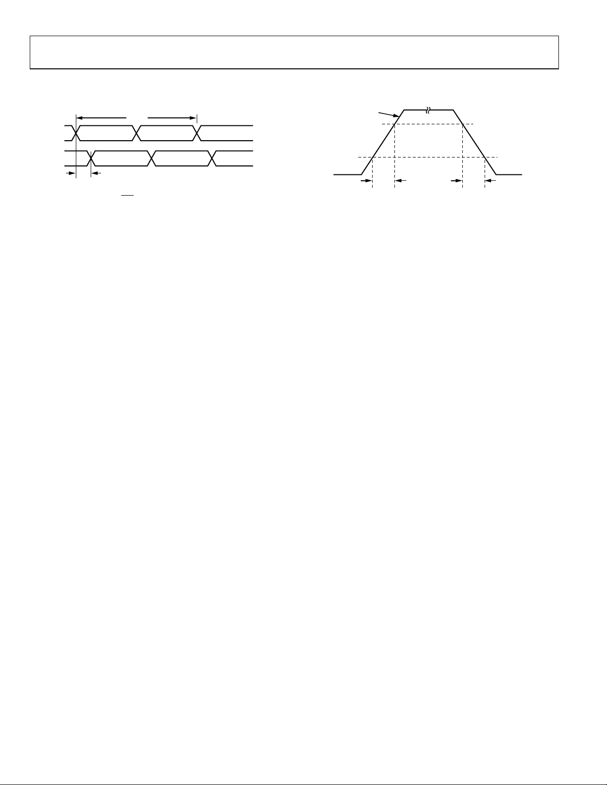
TIMING DIAGRAMS
t
CLK
CL
t
PECL
Figure 2. CLK/
CLK
to Clock Output Timing, DIV = 1
06430-060
DIFFERENTIAL
80%
20%
Figure 3. LVPECL Timing, Differential
LVPECL
t
RP
t
FP
06430-061
Rev. C | Page 12 of 64
Data Sheet AD9518-1
VCP to GND
−0.3 V to +5.8 V
ABSOLUTE MAXIMUM RATINGS
Table 17.
Parameter Rating
VS, VS_LVPECL to GND −0.3 V to +3.6 V
REFIN,
REFIN to
RSET to GND −0.3 V to VS + 0.3 V
CPRSET to GND −0.3 V to VS + 0.3 V
CLK,
CLK to
SCLK, SDIO, SDO, CS to GND −0.3 V to VS + 0.3 V
OUT0,
OUT3,
to GND
SYNC
REFMON, STATUS, LD to GND −0.3 V to VS + 0.3 V
Junction Temperature1 150°C
Storage Temperature Range −65°C to +150°C
Lead Temperature (10 sec) 300°C
1
See Table 18 for θJA.
to GND −0.3 V to VS + 0.3 V
REFIN
−3.3 V to +3.3 V
REFIN
to GND −0.3 V to VS + 0.3 V
CLK
−1.2 V to +1.2 V
CLK
, OUT1,
OUT0
,OUT4,
OUT3
to GND −0.3 V to VS + 0.3 V
OUT1
OUT4
, OUT2,
, OUT5,
OUT2
OUT5
,
−0.3 V to VS + 0.3 V
Stresses above those listed under Absolute Maximum Ratings
may cause permanent damage to the device. This is a stress
rating only; functional operation of the device at these or any
other conditions above those indicated in the operational
section of this specification is not implied. Exposure to absolute
maximum rating conditions for extended periods may affect
device reliability.
THERMAL RESISTANCE
Table 18.
Package Type1 θJA Unit
48-Lead LFCSP 24.7 °C/W
1
Thermal impedance measurements were taken on a 4-layer board in still air
in accordance with EIA/JESD51-2.
ESD CAUTION
Rev. C | Page 13 of 64

AD9518-1 Data Sheet
13141516171819
2021222324
SCLK
CS
SDO
SDIO
RESET
PD
OUT4
OUT4
VS_LVPECL
OUT5
OUT5
VS
4847464544434241403938
37
REFIN (REF1)
REFIN (REF2)
CPRSETVSRSETVSOUT0
OUT0
VS_LVPECL
OUT1
OUT1
VS
1
2
3
4
5
6
7
8
9
10
11
12
35
36
34
33
32
31
30
29
28
27
26
25
AD9518-1
TOP VIEW
(Not to S cale)
PIN 1
INDICATOR
CP
STATUS
CLK
VCP
REFMON
LD
BYPASS
VS
REF_SEL
LF
SYNC
CLK
OUT3
OUT2
VS
VS
VS_LVPECL
VS_LVPECL
OUT3
OUT2
NC
GND
VS
GND
06430-003
NOTES
1. NC = NO CONNECT.
2. THE EXTERNAL PADDLE ON THE BOTTOM OF THE PACKAGE MUST BE
CONNECTED T O GROUND FO R P ROPER OPERAT ION.
11 I Differential
CLK
Along with
, this is the self-biased differential input for the clock distribution section.
PIN CONFIGURATION AND FUNCTION DESCRIPTIONS
Table 19. Pin Function Descriptions
Input/
Pin No.
Output Pi n Type Mnemonic Description
1 O 3.3 V CMOS REFMON Reference Monitor (Output). This pin has multiple selectable outputs; see Table 44,
2 O 3.3 V CMOS LD Lock Detect (Output). This pin has multiple selectable outputs; see Table 44,
3 I Power VCP Power Supply for Charge Pump (CP). VS ≤ VCP ≤ 5.0 V. This pin is usually 3.3 V for most
4 O CP Charge Pump (Output). Connects to external loop filter.
5 O 3.3 V CMOS STATUS Status (Output). This pin has multiple selectable outputs; see Table 44, Register 0x017.
6 I 3.3 V CMOS REF_SEL Reference Select. Selects REF1 (low) or REF2 (high). This pin has an internal 30 kΩ
7 I 3.3 V CMOS
8 I Loop filter LF Loop Filter (Input). Connects to VCO control voltage node internally.
9 O Loop filter BYPA SS This pin is for bypassing the LDO to ground with a capacitor.
10, 24, 25,
I Power VS 3.3 V Power Pins.
26, 35, 37,
43, 45
SYNC
clock input
12 I Differential
clock input
Along with CLK, this is the self-biased differential input for the clock distribution section.
CLK
Figure 4. Pin Configuration
Register 0x01B.
Register 0x01A.
applications; but if a 5 V external VCXO is used, this pin should be 5 V.
pull-down resistor.
Manual Synchronizations and Manual Holdover. This pin initiates a manual
synchronization and is used for manual holdover. Active low. This pin has an internal
30 kΩ pull-up resistor.
This pin has 31 pF of internal capacitance to ground, which may influence the loop
filter design for large loop bandwidths.
CLK
This pin can be left floating if internal VCO is used.
This pin can be left floating if internal VCO is used.
Rev. C | Page 14 of 64
Data Sheet AD9518-1
20 O LVPECL
LVPECL Output; One Side of a Differential LVPECL Output.
Input/
Pin No.
13 I 3.3 V CMOS SCLK Serial Control Port Data Clock Signal.
14 I 3.3 V CMOS
15 O 3.3 V CMOS SDO Serial Control Port. Unidirectional serial data output.
16 I/O 3.3 V CMOS SDIO Serial Control Port. Bidirectional serial data input/output.
17 I 3.3 V CMOS
18 I 3.3 V CMOS
19 O LVPECL OUT4 LVPECL Output; One Side of a Differential LVPECL Output.
21, 30, 31,
40
22 O LVPECL OUT5 LVPECL Output; One Side of a Differential LVPECL Output.
23 O LVPECL
27, 34 GND GND Ground. See the description for EPAD.
28 O LVPECL
29 O LVPECL OUT3 LVPECL Output; One Side of a Differential LVPECL Output.
32 O LVPECL
33 O LVPECL OUT2 LVPECL Output; One Side of a Differential LVPECL Output.
36 NC No Connection.
38 O LVPECL
39 O LVPECL OUT1 LVPECL Output; One Side of a Differential LVPECL Output.
41 O LVPECL
42 O LVPECL OUT0 LVPECL Output; One Side of a Differential LVPECL Output.
44 O Current set
46 O Current set
47 I Reference
48 I Reference
EPAD GND GND Ground. The external paddle on the bottom of the package must be connected to
Output Pi n Type Mnemonic Description
Serial Control Port Chip Select, Active Low. This pin has an internal 30 kΩ pull-up
CS
resistor.
Chip Reset, Active Low. This pin has an internal 30 kΩ pull-up resistor.
RESET
Chip Power Down, Active Low. This pin has an internal 30 kΩ pull-up resistor.
PD
OUT4
I Power VS_LVPECL Extended Voltage 2.5 V to 3.3 V LVPECL Power Pins.
LVPECL Output; One Side of a Differential LVPECL Output.
OUT5
LVPECL Output; One Side of a Differential LVPECL Output.
OUT3
LVPECL Output; One Side of a Differential LVPECL Output.
OUT2
LVPECL Output; One Side of a Differential LVPECL Output.
OUT1
LVPECL Output; One Side of a Differential LVPECL Output.
OUT0
RSET Resistor connected here sets internal bias currents. Nominal value = 4.12 kΩ.
resistor
CPRSET Resistor connected here sets the CP current range. Nominal value = 5.1 kΩ.
resistor
(REF2) Along with REFIN, this is the self-biased differential input for the PLL reference.
REFIN
input
REFIN (REF1) Along with
input
Alternatively, this pin is a single-ended input for REF2.
, this is the self-biased differential input for the PLL reference.
REFIN
Alternatively, this pin is a single-ended input for REF1.
ground for proper operation.
Rev. C | Page 15 of 64
AD9518-1 Data Sheet
0 500 1000 1500 2000 2500 3000
CURRENT (mA)
FREQUENCY (MHz)
300
100
120
140
160
180
200
220
240
260
280
3 CHANNELS—6 LV P E CL
3 CHANNELS—3 LV P E CL
2 CHANNELS—2 LV P E CL
1 CHANNEL—1 LVP E CL
06430-007
65
35
40
45
50
55
60
2.3 2.72.62.52.4
K
VCO
(MHz/V)
VCO FREQ UE NCY ( GHz)
06430-010
5.0
4.5
4.0
3.5
3.0
2.5
2.0
1.5
1.0
0.5
0
0 0.5 1.0 1.5 2.0 2.5 3.0
CURRENT FROM CP P IN (mA)
VOLTAGE ON CP PIN (V)
PUMP DOWN PUMP UP
06430-011
5.0
4.5
4.0
3.5
3.0
2.5
2.0
1.5
1.0
0.5
0
0 0.5 1.0 1.5 2.0 3.0 4.02.5 3.5 5.04.5
CURRENT FROM CP P IN (mA)
VOLTAGE ON CP PIN (V)
PUMP DOWN PUMP UP
06430-012
–140
–145
–150
–155
–160
–165
–170
0.1 1 10010
PFD PHASE NO ISE REFERRED TO PFD INP UT
(dBc/Hz)
PFD FREQUENCY (MHz)
06430-013
–210
–224
–222
–220
–218
–216
–214
–212
0 2.52.01.51.00.5
PLL FIGURE OF MERIT (dBc/Hz)
SLEW RATE (V/ns)
06430-136
TYPICAL PERFORMANCE CHARACTERISTICS
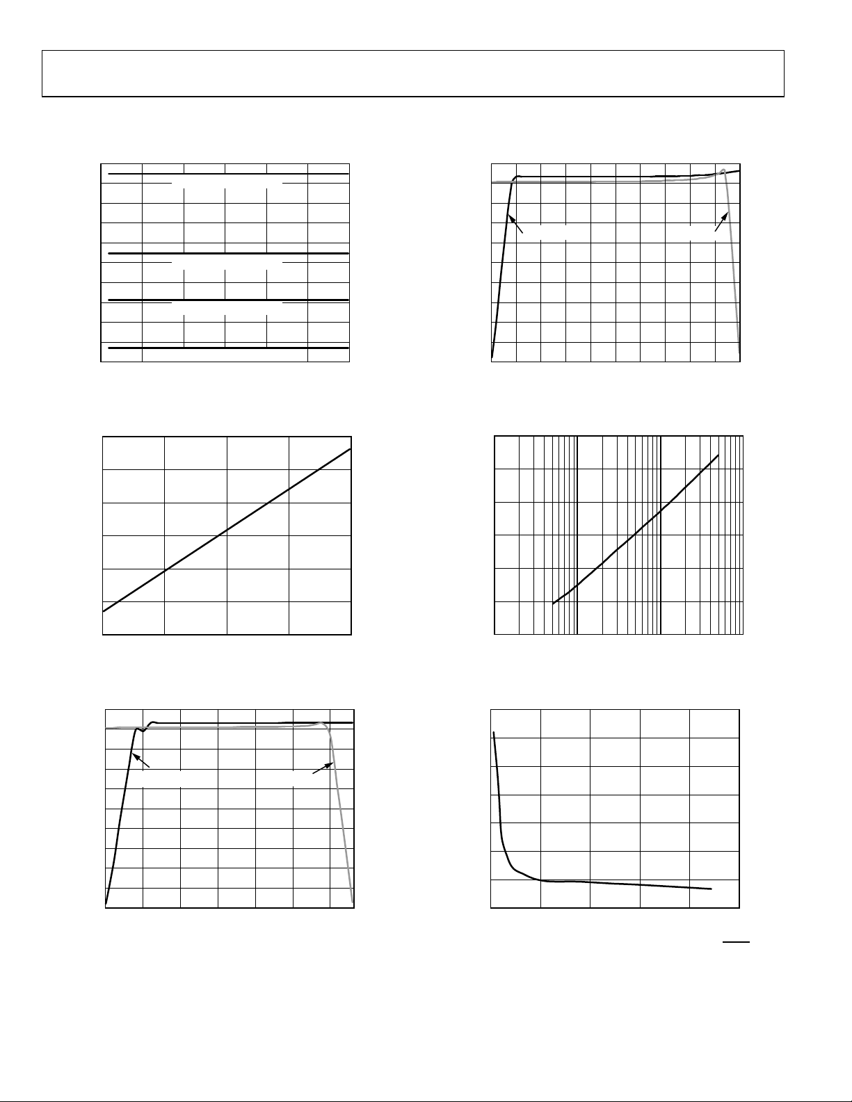
Figure 5. Current vs. Frequency, Direct to Output, LVPECL Outputs
Figure 6. K
vs. VCO Frequency
VCO
Figure 8. Charge Pump Characteristics at VCP = 5.0 V
Figure 9. PFD Phase Noise Referred to PFD Input vs. PFD Frequency
Figure 7. Charge Pump Characteristics at VCP = 3.3 V
Figure 10. PLL Figure of Merit (FOM) vs. Slew Rate at REFIN/
REFIN
Rev. C | Page 16 of 64
Data Sheet AD9518-1
1.9
1.8
1.7
1.6
1.5
1.4
1.3
1.2
2.3 2.4 2.5 2.6 2.7
VCO TUNING VOLTAGE (V)
FREQUENCY ( GHz)
06430-138
–110
–100
–90
–80
–70
–60
–50
–40
–30
–20
–10
10
0
CENTER 122.88MHz SPAN 50 M Hz5MHz/DIV
RELATIVE POWER (dB)
06430-137
–110
–100
–90
–80
–70
–60
–50
–40
–30
–20
–10
10
0
CENTER 122.88MHz SPAN 1MHz100kHz/DIV
RELATIVE POWER (dB)
06430-135
1.0
0.6
0.2
–0.2
–0.6
–1.0
0 252015105
DIFFERENTIAL OUTPUT (V)
TIME (ns)
06430-014
1.0
0.6
0.2
–0.2
–0.6
–1.0
0 21
DIFFERENTIAL OUTPUT (V)
TIME (ns)
06430-015
1600
800
1000
1200
1400
0 321
DIFFERENTIAL SWING (mV p-p)
FREQUENCY ( GHz)
06430-020
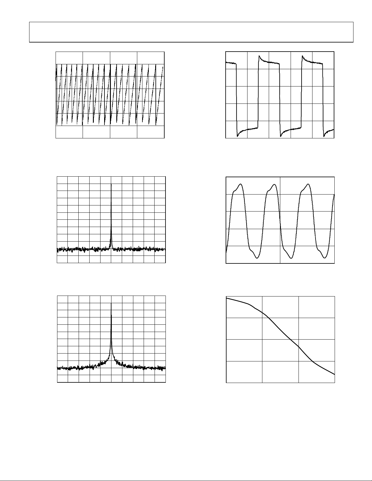
Figure 11. VCO Tuning Voltage vs. Frequency
(Note that VCO calibration centers the dc tuning voltage
for the PLL setup that is active during calibration.)
Figure 12. PFD/CP Spurs; 122.88 MHz; PFD = 15.36 MHz;
LBW = 55 kHz; I
= 4.8 mA; f
CP
= 2.46 GHz
VCO
Figure 14. LVPECL Output (Differential) at 100 MHz
Figure 15. LVPECL Output (Differential) at 1600 MHz
Figure 13. Output Spectrum, LVPECL; 122.88 MHz; PFD = 15.36 MHz;
LBW = 55 kHz; I
= 4.8 mA; f
CP
= 2.46 GHz
VCO
Figure 16. LVPECL Differential Swing vs. Frequency,
Using a Differential Probe Across the Output Pair
Rev. C | Page 17 of 64
AD9518-1 Data Sheet
–70
–80
–90
–100
–110
–120
–130
–140
–150
10k 100M10M1M100k
PHASE NOISE (dBc/Hz)
FREQUENCY ( Hz )
06430-023
–70
–80
–90
–100
–110
–120
–130
–140
–150
10k 100M10M1M100k
PHASE NOISE (dBc/Hz)
FREQUENCY ( Hz )
06430-024
–70
–80
–90
–100
–110
–120
–130
–140
–150
10k 100M10M1M100k
PHASE NOISE (dBc/Hz)
FREQUENCY ( Hz )
06430-025
–120
–130
–125
–135
–140
–145
–150
–155
–160
10 100M10M1M100k10k1k100
PHASE NOISE (dBc/Hz)
FREQUENCY ( Hz )
06430-026
–110
–120
–130
–140
–150
–160
10 100M10M1M100k10k1k100
PHASE NOISE (dBc/Hz)
FREQUENCY ( Hz )
06430-027
–100
–110
–120
–130
–140
–150
10 100M10M1M100k10k1k100
PHASE NOISE (dBc/Hz)
FREQUENCY ( Hz )
06430-128
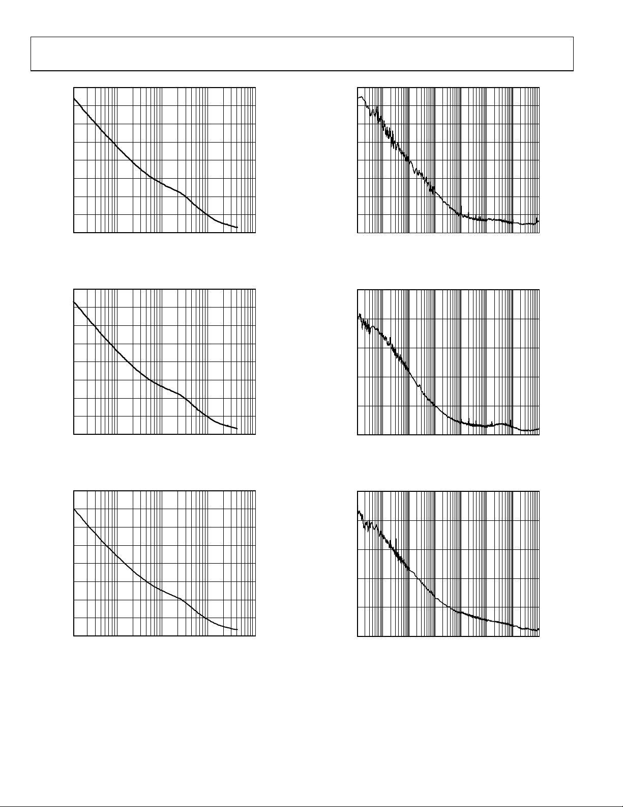
Figure 17. Internal VCO Phase Noise (Absolute) Direct to LVPECL at 2650 MHz
Figure 18. Internal VCO Phase Noise (Absolute) Direct to LVPECL at 2475 MHz
Figure 20. Phase Noise (Additive) LVPECL at 245.76 MHz, Divide-by-1
Figure 21. Phase Noise (Additive) LVPECL at 200 MHz, Divide-by-5
Figure 19. Internal VCO Phase Noise (Absolute) Direct to LVPECL at 2300 MHz
Figure 22. Phase Noise (Additive) LVPECL at 1600 MHz, Divide-by-1
Rev. C | Page 18 of 64
Data Sheet AD9518-1
–120
–160
–150
–140
–130
1k 100M10M1M100k10k
PHASE NOISE (dBc/Hz)
FREQUENCY ( Hz )
06430-141
–70
–80
–90
–100
–110
–120
–130
–140
–150
–160
1k 100M10M1M100k10k
PHASE NOISE (dBc/Hz)
FREQUENCY ( Hz )
06430-139
–120
–160
–150
–140
–130
1k 100M10M1M100k10k
PHASE NOISE (dBc/Hz)
FREQUENCY ( Hz )
06430-140
1000
100
10
1
0.1
0.01 0.1 1 10 100 1000
INPUT JITTER AMPLITUDE (UI p-p)
JITTER F RE QUENCY (kHz)
06430-148
OC-48 OBJECTIVE MASK
AD9518
NOTE: 375UI M AX AT 10Hz OFFS E T IS THE
MAXIMUM JITTER THAT CAN BE
GENERATED BY THE TEST EQUIPMENT.
FAILURE POINT IS GREATER THAN 375UI .
f
OBJ
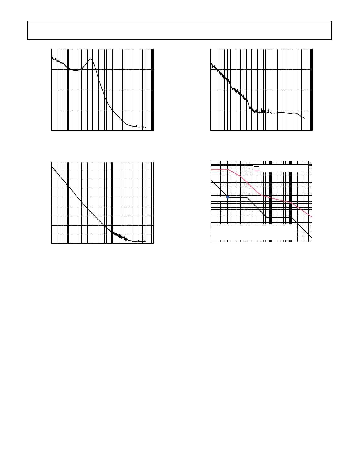
Figure 23. Phase Noise (Absolute) Clock Generation; Internal VCO at
2.4576 GHz; PFD = 15.36 MHz; LBW = 55 kHz; LVPECL Output = 122.88 MHz
Figure 24. Phase Noise (Absolute) Clock Cleanup; Internal VCO at 2.488 GHz;
PFD = 19.44 MHz; LBW = 12.8 kHz; LVPECL Output = 155.52 MHz
Figure 25. Phase No ise (Absolute); External VCXO (Toyocom TCO-2112) at
245.76 MHz; PFD = 15.36 MHz; LBW = 25 0 Hz; LVPECL Output = 245.76 MHz
Figure 26. GR-253 Jitter Tolerance Plot
Rev. C | Page 19 of 64

AD9518-1 Data Sheet
TERMINOLOGY
Phase Jitter and Phase Noise
An ideal sine wave can be thought of as having a continuous
and even progression of phase with time from 0° to 360° for
each cycle. Actual signals, however, display a certain amount
of variation from ideal phase progression over time. This
phenomenon is called phase jitter. Although many causes can
contribute to phase jitter, one major cause is random noise,
which is characterized statistically as being Gaussian (normal)
in distribution.
This phase jitter leads to a spreading out of the energy of the
sine wave in the frequency domain, producing a continuous
power spectrum. This power spectrum is usually reported as a
series of values whose units are dBc/Hz at a given offset in
frequency from the sine wave (carrier). The value is a ratio
(expressed in dB) of the power contained within a 1 Hz
bandwidth with respect to the power at the carrier frequency.
For each measurement, the offset from the carrier frequency is
also given.
It is meaningful to integrate the total power contained within
some interval of offset frequencies (for example, 10 kHz to
10 MHz). This is called the integrated phase noise over that
frequency offset interval and can be readily related to the time
jitter due to the phase noise within that offset frequency interval.
Phase noise has a detrimental effect on the performance of
ADCs, DACs, and RF mixers. It lowers the achievable dynamic
range of the converters and mixers, although they are affected
in somewhat different ways.
Time Jitter
Phase noise is a frequency domain phenomenon. In the time
domain, the same effect is exhibited as time jitter. When
observing a sine wave, the time of successive zero crossings
varies. In a square wave, the time jitter is a displacement of the
edges from their ideal (regular) times of occurrence. In both
cases, the variations in timing from the ideal are the time jitter.
Because these variations are random in nature, the time jitter is
specified in units of seconds root mean square (rms) or 1 sigma
of the Gaussian distribution.
Time jitter that occurs on a sampling clock for a DAC or an
ADC decreases the signal-to-noise ratio (SNR) and dynamic
range of the converter. A sampling clock with the lowest possible
jitter provides the highest performance from a given converter.
Additive Phase Noise
Additive phase noise is the amount of phase noise that can be
attributed to the device or subsystem being measured. The phase
noise of any external oscillators or clock sources is subtracted.
This makes it possible to predict the degree to which the device
impacts the total system phase noise when used in conjunction
with the various oscillators and clock sources, each of which
contributes its own phase noise to the total. In many cases, the
phase noise of one element dominates the system phase noise.
When there are multiple contributors to phase noise, the total
is the square root of the sum of squares of the individual
contributors.
Additive Time Jitter
Additive time jitter is the amount of time jitter that can be
attributed to the device or subsystem being measured. The time
jitter of any external oscillators or clock sources is subtracted. This
makes it possible to predict the degree to which the device impacts
the total system time jitter when used in conjunction with the
various oscillators and clock sources, each of which contributes
its own time jitter to the total. In many cases, the time jitter of
the external oscillators and clock sources dominates the system
time jitter.
Rev. C | Page 20 of 64
 Loading...