14-Output Clock Generator with
www.BDTIC.com/ADI
FEATURES
Low phase noise, phase-locked loop
On-chip VCO tunes from 2.55 GHz to 2.95 GHz
External VCO/VCXO to 2.4 GHz optional
One differential or two single-ended reference inputs
Reference monitoring capability
Auto and manual reference switchover/holdover modes
Autorecover from holdover
Accepts references to 250 MHz
Programmable delays in path to PFD
Digital or analog lock detect, selectable
3 pairs of 1.6 GHz LVPECL outputs
Each pair shares 1 to 32 divider with coarse phase delay
Additive output jitter 225 f
Channel-to-channel skew paired outputs <10 ps
2 pairs of 800 MHz LVDS clock outputs
Each pair shares two cascaded 1 to 32 dividers with coarse
phase del
ay
Additive output jitter 275 f
Fine delay adjust (ΔT) on each LVDS output
Eight 250 MHz CMOS outputs (two per LVDS output)
Automatic synchronization of all outputs on power-up
Manual synchronization of outputs as needed
Serial control port
64-lead LFCSP
APPLICATIONS
Low jitter, low phase noise clock distribution
Clocking high speed ADCs, DACs, DDSs, DDCs, DUCs, MxFEs
High performance wireless transceivers
High performance instrumentation
Broadband infrastructure
AT E
GENERAL DESCRIPTION
The AD9516-01 provides a multi-output clock distribution
function with subpicosecond jitter performance, along with an onchip PLL and VCO. The on-chip VCO tunes from 2.55 GHz to
2.95 GHz. Optionally, an external VCO/VCXO of up to 2.4 GHz
may be used.
The AD9516-0 emphasizes low jitter and phase noise to
max
imize data converter performance, and can benefit other
applications with demanding phase noise and jitter requirements.
rms
S
rms
S
Integrated 2.8 GHz VCO
AD9516-0
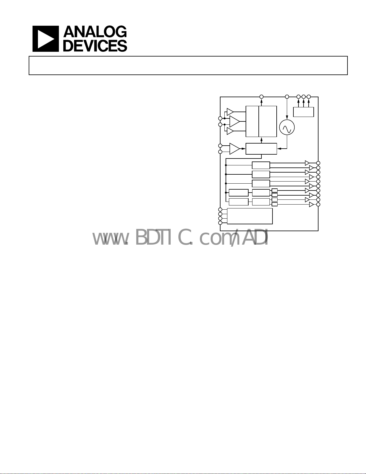
FUNCTIONAL BLOCK DIAGRAM
PLL
ΔT
ΔT
ΔT
ΔT
LF
STATUS
MONITOR
VCO
LVPECL
LVPECL
LVPECL
LVDS/CMOS
LVDS/CMOS
AD9516-0
CP
REF1
REFIN
REF2
SWITCHOVER
AND MONI TOR
CLK
DIV/Φ DIV/Φ
DIV/Φ DIV/Φ
SERIAL CONT ROL PORT
DIVIDER
AND MUXs
DIV/Φ
DIV/Φ
DIV/Φ
AND
DIGITAL LOGIC
Figure 1.
The AD9516-0 features six LVPECL outputs (in three pairs);
four LVDS outputs (in two pairs); and eight CMOS outputs
(two per LVDS output). The LVPECL outputs operate to
1.6 GHz, the LVDS outputs operate to 800 MHz, and the CMOS
outputs operate to 250 MHz.
Each pair of outputs has dividers that allow both the divide
atio and coarse delay (or phase) to be set. The range of division
r
for the LVPECL outputs is 1 to 32. The LVDS/CMOS outputs
allow a range of divisions up to a maximum of 1024.
The AD9516-0 is available in a 64-lead LFCSP and can be
op
erated from a single 3.3 V supply. An external VCO, which
requires an extended voltage range, can be accommodated
by connecting the charge pump supply (VCP) to 5.5 V. A
separate LVPECL power supply can be from 2.375 V to 3.6 V.
The AD9516-0 is specified for operation over the industrial
nge of −40°C to +85°C.
ra
1
AD9516 is used throughout to refer to all the members of the AD9516
family. However, when AD9516-0 is used it is referring to that specific
member of the AD9516 family.
OUT0
OUT1
OUT2
OUT3
OUT4
OUT5
OUT6
OUT7
OUT8
OUT9
06419-001
Rev. 0
Information furnished by Analog Devices is believed to be accurate and reliable. However, no
responsibility is assumed by Anal og Devices for its use, nor for any infringements of patents or ot her
rights of third parties that may result from its use. Specifications subject to change without notice. No
license is granted by implication or otherwise under any patent or patent rights of Analog Devices.
Trademarks and registered trademarks are the property of their respective owners.
One Technology Way, P.O. Box 9106, Norwood, MA 02062-9106, U.S.A.
Tel: 781.329.4700 www.analog.com
Fax: 781.461.3113 ©2007 Analog Devices, Inc. All rights reserved.

AD9516-0
www.BDTIC.com/ADI
TABLE OF CONTENTS
Features .............................................................................................. 1
Applications....................................................................................... 1
General Description......................................................................... 1
Functional Block Diagram .............................................................. 1
Revision History ............................................................................... 3
Specifications..................................................................................... 4
Power Supply Requirements ....................................................... 4
PLL Characteristics ...................................................................... 4
Clock Inputs.................................................................................. 6
Clock Outputs............................................................................... 6
Timing Characteristics ................................................................ 7
Clock Output Additive Phase Noise (Distribution Only; VCO
Divider Not Used) ........................................................................ 8
Clock Output Absolute Phase Noise (Internal VCO Used).... 9
Clock Output Absolute Time Jitter (Clock Generation Using
Internal VCO) ............................................................................. 10
Clock Output Absolute Time Jitter (Clock Cleanup Using
Internal VCO) ............................................................................. 10
Clock Output Absolute Time Jitter (Clock Generation Using
External VCXO) ......................................................................... 10
Clock Output Additive Time Jitter (VCO Divider Not Used)
....................................................................................................... 11
Clock Output Additive Time Jitter (VCO Divider Used)..... 11
Delay Block Additive Time Jitter.............................................. 12
Serial Control Port .....................................................................12
SYNC
PD
,
LD, STATUS, REFMON Pins.................................................... 13
Power Dissipation....................................................................... 14
Timing Diagrams............................................................................ 15
Absolute Maximum Ratings.......................................................... 16
Thermal Resistance .................................................................... 16
ESD Caution................................................................................ 16
Pin Configuration and Function Descriptions........................... 17
Typical Performance Characteristics ........................................... 19
Te r mi n ol o g y .................................................................................... 25
Detailed Block Diagram ................................................................ 26
Theory of Operation ...................................................................... 27
Operational Configurations...................................................... 27
High Frequency Clock Distribution—CLK or External
VCO >1600 MHz ...................................................................27
Internal VCO and Clock Distribution.................................29
, and
RESET
Pins ..................................................... 13
Clock Distribution or External VCO <1600 MHz ............ 31
Phase-Locked Loop (PLL) .................................................... 33
Configuration of the PLL ...................................................... 33
Phase Frequency Detector (PFD) ........................................ 33
Charge Pump (CP)................................................................. 34
On-Chip VCO ........................................................................ 34
PLL External Loop Filter....................................................... 34
PLL Reference Inputs............................................................. 34
Reference Switchover............................................................. 35
Reference Divider R............................................................... 35
VCXO/VCO Feedback Divider N: P, A, B, R ..................... 35
Digital Lock Detect (DLD) ....................................................... 37
Analog Lock Detect (ALD)................................................... 37
Current Source Digital Lock Detect (DLD) ....................... 37
External VCXO/VCO Clock Input (CLK/
Holdover .................................................................................. 38
Manual Holdover Mode ........................................................ 38
Automatic/Internal Holdover Mode.................................... 38
Frequency Status Monitors................................................... 39
VCO Calibration .................................................................... 40
Clock Distribution ..................................................................... 41
Internal VCO or External CLK as Clock Source ............... 41
CLK or VCO Direct to LVPECL Outputs........................... 41
Clock Frequency Division..................................................... 42
VCO Divider ........................................................................... 42
Channel Dividers—LVPECL Outputs................................. 42
Channel Dividers—LVDS/CMOS Outputs........................ 44
Synchronizing the Outputs—SYNC Function ................... 47
Clock Outputs......................................................................... 49
LVPECL Outputs: OUT0 to OUT5 ..................................... 49
LVDS/CMOS Outputs: OUT6 to OUT9............................. 50
Reset Modes ................................................................................ 50
Power-On Reset—Start-Up Conditions when
V
Is Applied ........................................................................... 50
S
Asynchronous Reset via the
Soft Reset via 0x00<5> .......................................................... 50
Power-Down Modes .................................................................. 50
Chip Power-Down via
PLL Power-Down................................................................... 51
Distribution Power-Down .................................................... 51
RESET
PD
.................................................... 50
CLK
)................ 37
Pin ............................. 50
Rev. 0 | Page 2 of 84

AD9516-0
www.BDTIC.com/ADI
Individual Clock Output Power-Down................................51
Individual Circuit Block Power-Down ................................51
Serial Control Port ..........................................................................52
Serial Control Port Pin Descriptions........................................52
General Operation of Serial Control Port ...............................52
Communication Cycle—Instruction Plus Data..................52
Wr it e .........................................................................................52
Read ..........................................................................................53
The Instruction Word (16 Bits).................................................53
MSB/LSB First Transfers............................................................53
REVISION HISTORY
4/07—Revision 0: Initial Version
Register Map Overview ..................................................................56
Register Map Descriptions.............................................................60
Application Notes............................................................................79
Using the AD9516 Outputs for ADC Clock Applications ....79
LVPECL Clock D i s t ribut io n ......................................................79
LVDS Clock Distribution...........................................................79
CMOS Clock Distribution.........................................................80
Outline Dimensions........................................................................81
Ordering Guide...........................................................................81
Rev. 0 | Page 3 of 84

AD9516-0
www.BDTIC.com/ADI
SPECIFICATIONS
Typical (typ) is given for VS = V
unless otherwise noted. Minimum (min) and maximum (max) values are given over full V
POWER SUPPLY REQUIREMENTS
Table 1.
Parameter Min Typ Max Unit Test Conditions/Comments
V
S
V
S_LVPECL
V
CP
3.135 3.3 3.465 V This is 3.3 V ± 5%
2.375 V
V
S
RSET Pin Resistor 4.12 kΩ Sets internal biasing currents; connect to ground
CPRSET Pin Resistor 5.1 kΩ
BYPASS Pin Capacitor 220 nF Bypass for internal LDO regulator; necessary for LDO stability; connect to ground
PLL CHARACTERISTICS
Table 2.
Parameter Min Typ Max Unit Test Conditions/Comments
VCO (ON-CHIP)
Frequency Range 2550 2950 MHz See Figure 15
VCO Gain (K
Tunin g Volt age (VT) 0.5 VCP − 0.5 V
Frequency Pushing (Open-Loop) 1 MHz/V
Phase Noise @ 100 kHz Offset −105 dBc/Hz f = 2800 MHz
Phase Noise @ 1 MHz Offset −123 dBc/Hz f = 2800 MHz
REFERENCE INPUTS
Differential Mode (REFIN, REFIN)
Input Frequency 0 250 MHz
Input Sensitivity 250 mV p-p
Self-Bias Voltage, REFIN 1.35 1.60 1.75 V Self-bias voltage of REFIN
Self-Bias Voltage, REFIN
Input Resistance, REFIN 4.0 4.8 5.9 kΩ Self-biased
Input Resistance, REFIN
Dual Single-Ended Mode (REF1, REF2) Two single-ended CMOS-compatible inputs
Input Frequency (AC-Coupled) 20 250 MHz Slew rate > 50 V/μs
Input Frequency (DC-Coupled) 0 250 MHz Slew rate > 50 V/μs; CMOS levels
Input Sensitivity (AC-Coupled) 0.8 V p-p Should not exceed VS p-p
Input Logic High 2.0 V
Input Logic Low 0.8 V
Input Current −100 +100 μA
Input Capacitance 2 pF
) 50 MHz/V See Figure 10
VCO
= 3.3 V ± 5%; VS ≤ VCP ≤ 5.25 V; TA = 25°C; R
S_LVPECL
V This is nominally 2.5 V to 3.3 V ± 5%
S
SET
5.25 V This is nominally 3.3 V to 5.0 V ± 5%
Sets internal CP current range, nominally 4.8 mA (CP_lsb = 600 μA);
tual current can be calculated by: CP_lsb = 3.06/CPRSET; connect to ground
ac
1.30 1.50 1.60 V
4.4 5.3 6.4 kΩ Self-biased
= 4.12 kΩ; CP
and TA (−40°C to +85°C) variation.
S
≤ VS when using internal VCO; outside of this
V
CP
= 5.1 kΩ,
RSET
range, the CP spurs may increase due to CP up/
down mismatch
Differential mode (can accommodate singleended input by ac grounding undriven input)
Frequencies below about 1 MHz should be
coupled; be careful to match V
dc-
(self-bias voltage)
CM
PLL figure of merit will increase with increasing
te; see Figure 14
slew ra
Self-bias voltage of REFIN
1
1
Each pin, REFIN/REFIN
1
1
(REF1/REF2)
Rev. 0 | Page 4 of 84

AD9516-0
www.BDTIC.com/ADI
Parameter Min Typ Max Unit Test Conditions/Comments
PHASE/FREQUENCY DETECTOR (PFD)
PFD Input Frequency 100 MHz Antibacklash pulse width = 1.3 ns, 2.9 ns
45 MHz Antibacklash pulse width = 6.0 ns
Antibacklash Pulse Width 1.3 ns 0x17<1:0> = 01b
2.9 ns 0x17<1:0> = 00b; 0x17<1:0> = 11b
6.0 ns 0x17<1:0> = 10b
CHARGE PUMP (CP)
ICP Sink/Source Programmable
High Value 4.8 mA With CP
Low Value 0.60 mA
Absolute Accuracy 2.5 % CPV = VCP/2
CP
Range 2.7/10 kΩ
RSET
ICP High Impedance Mode Leakage 1 nA
Sink-and-Source Current Matching 2 % 0.5 < CPV < VCP − 0.5 V
ICP vs. CP
ICP vs. Temperature 2 % CPV = VCP/2 V
PRESCALER (PART OF N DIVIDER)
Prescaler Input Frequency
Prescaler Output Frequency 300 MHz
PLL DIVIDER DELAYS Register 0x19: R <5:3>, N <2:0>; see Table 53
000 Off ps
001 330 ps
010 440 ps
011 550 ps
100 660 ps
101 770 ps
110 880 ps
111 990 ps
NOISE CHARACTERISTICS
In-Band Phase Noise of the Charge
Pump/Phase Frequency Detector
(In-Band Means Within the LBW
of the PLL)
PLL Figure of Merit (FOM) −220 dBc/Hz
V
P = 1 FD 300 MHz
P = 2 FD 600 MHz
P = 3 FD 900 MHz
P = 2 DM (2/3) 600 MHz
P = 4 DM (4/5) 1000 MHz
P = 8 DM (8/9) 2400 MHz
P = 16 DM (16/17) 3000 MHz
P = 32 DM (32/33) 3000 MHz
@ 500 kHz PFD Frequency −165 dBc/Hz
@ 1 MHz PFD Frequency −162 dBc/Hz
@ 10 MHz PFD Frequency −151 dBc/Hz
@ 50 MHz PFD Frequency −143 dBc/Hz
1.5 % 0.5 < CPV < VCP − 0.5 V
A, B counter input frequency (prescaler
input fr
The PLL in-band phase noise floor is estimated
by measuring the in-band phase noise at the
output of the VCO and subtracting 20log(N)
(where N is the value of the N divider)
Reference slew rate > 0.25 V/ns. FOM +10log (f
is an approximation of the PFD/CP in-band
phase noise (in the flat region) inside the PLL
loop bandwidth. When running closed loop,
the phase noise, as observed at the VCO output,
is increased by 20log(N)
= 5.1 kΩ
RSET
equency divided by P)
PFD
)
Rev. 0 | Page 5 of 84

AD9516-0
www.BDTIC.com/ADI
Parameter Min Typ Max Unit Test Conditions/Comments
PLL DIGITAL LOCK DETECT WINDOW
Required to Lock (Coincidence of Edges) Selected by 0x17<1:0> and 0x18<4>
Low Range (ABP 1.3 ns, 2.9 ns) 3.5 ns 0x17<1:0> = 00b, 01b,11b; 0x18<4> = 1b
High Range (ABP 1.3 ns, 2.9 ns) 7.5 ns 0x17<1:0> = 00b, 01b, 11b; 0x18<4> = 0b
High Range (ABP 6 ns) 3.5 ns 0x17<1:0> = 10b; 0x18<4> = 0b
To Unlock After Lock (Hysteresis)
Low Range (ABP 1.3 ns, 2.9 ns) 7 ns 0x17<1:0> = 00b, 01b, 11b; 0x18<4> = 1b
High Range (ABP 1.3 ns, 2.9 ns) 15 ns 0x17<1:0> = 00b, 01b, 11b; 0x18<4> = 0b
High Range (ABP 6 ns) 11 ns 0x17<1:0> = 10b; 0x18<4> = 0b
1
REFIN and
2
For reliable operation of the digital lock detect, the period of the PFD frequency must be greater than the unlock-after-lock time.
REFIN
self-bias points are offset slightly to avoid chatter on an open input condition.
CLOCK INPUTS
Table 3.
Parameter Min Typ Max Unit Test Conditions/Comments
CLOCK INPUTS (CLK, CLK)
Input Frequency 0
0
Input Sensitivity, Differential 150 mV p-p
Input Level, Differential 2 V p-p
Input Common-Mode Voltage, V
Input Common-Mode Range, V
Input Sensitivity, Single-Ended 150 mV p-p
Input Resistance 3.9 4.7 5.7 kΩ Self-biased
Input Capacitance 2 pF
1
Below about 1 MHz, the input should be dc-coupled. Care should be taken to match VCM.
CMR
2
2
Signal available at LD, STATUS, and REFMON pins
when se
lected by appropriate register settings
Differential input
1
2.4 GHz High frequency distribution (VCO divider)
1
1.6 GHz Distribution only (VCO divider bypassed)
Measured at 2.4 GHz. Jitter performance is improved
w rates > 1 V/ns
with sle
Larger voltage swings may turn on the protection
diodes and can degr
CM
1.3 1.57 1.8 V Self-biased; enables ac coupling
ade jitter performance
1.3 1.8 V With 200 mV p-p signal applied; dc-coupled
CLK ac-coupled; CLK
ac-bypassed to RF ground
CLOCK OUTPUTS
Table 4.
Parameter Min Typ Max Unit Test Conditions/Comments
LVPECL CLOCK OUTPUTS Termination = 50 Ω to VS − 2 V
OUT0, OUT1, OUT2, OUT3, OUT4, OUT5
Differential (OUT, OUT
Output Frequency, Maximum 2950 MHz Using direct to output; see Figure 25
Output High Voltage (VOH) VS − 1.12 VS − 0.98 VS − 0.84 V
Output Low Voltage (VOL) VS − 2.03 VS − 1.77 VS − 1.49 V
Output Differential Voltage (VOD) 550 790 980 mV
LVDS CLOCK OUTPUTS Differential termination 100 Ω @ 3.5 mA
OUT6, OUT7, OUT8, OUT9
Differential (OUT, OUT
Output Frequency 800 MHz See Figure 26
Differential Output Voltage (VOD) 247 360 454 mV
Delta V
OD
25 mV
Output Offset Voltage (VOS) 1.125 1.24 1.375 V
Delta V
OS
25 mV
Short-Circuit Current (ISA, ISB) 14 24 mA Output shorted to GND
Rev. 0 | Page 6 of 84
)
)
AD9516-0
www.BDTIC.com/ADI
Parameter Min Typ Max Unit Test Conditions/Comments
CMOS CLOCK OUTPUTS
OUT6A, OUT6B, OUT7A, OUT7B, OUT8A,
OUT8B, OUT9A, OUT9B
Output Frequency 250 MHz see Figure 27
Output Voltage High (VOH) VS − 0.1 V @ 1 mA load
Output Voltage Low (VOL) 0.1 V @ 1 mA load
TIMING CHARACTERISTICS
Table 5.
Parameter Min Typ Max Unit Test Conditions/Comments
LVPECL Termination = 50 Ω to VS − 2 V; level = 810 mV
Output Rise Time, t
Output Fall Time, t
PROPAGATION DELAY, t
High Frequency Clock Distribution Configuration 835 995 1180 ps See Figure 42
Clock Distribution Configuration 773 933 1090 ps See Figure 44
Variation with Temperature 0.8 ps/°C
OUTPUT SKEW, LVPECL OUTPUTS
LVPECL Outputs That Share the Same Divider 5 15 ps
LVPECL Outputs on Different Dividers 13 40 ps
All LVPECL Outputs Across Multiple Parts 220 ps
LVDS Termination = 100 Ω differential; 3.5 mA
Output Rise Time, t
Output Fall Time, t
PROPAGATION DELAY, t
OUT6, OUT7, OUT8, OUT9
For All Divide Values 1.4 1.8 2.1 ns
Variation with Temperature 1.25 ps/°C
OUTPUT SKEW, LVDS OUTPUTS
LVDS Outputs That Share the Same Divider 6 62 ps
LVDS Outputs on Different Dividers 25 150 ps
All LVDS Outputs Across Multiple Parts 430 ps
CMOS Termination = open
Output Rise Time, t
Output Fall Time, t
PROPAGATION DELAY, t
For All Divide Values 1.6 2.1 2.6 ns
Variation with Temperature 2.6 ps/°C
OUTPUT SKEW, CMOS OUTPUTS
CMOS Outputs That Share the Same Divider 4 66 ps
All CMOS Outputs on Different Dividers 28 180 ps
All CMOS Outputs Across Multiple Parts 675 ps
DELAY ADJUST
Shortest Delay Range
Zero Scale 50 315 680 ps 0xA2 (0xA5) (0xA8) (0xAB) <5:0> 000000b
Full Scale 540 880 1180 ps 0xA2 (0xA5) (0xA8) (0xAB) <5:0> 101111b
Longest Delay Range
Zero Scale 200 570 950 ps 0xA2 (0xA5) (0xA8) (0xAB) <5:0> 000000b
Quarter Scale 1.72 2.31 2.89 ns 0xA2 (0xA5) (0xA8) (0xAB) <5:0> 001100b
Full Scale 5.7 8.0 10.1 ns 0xA2 (0xA5) (0xA8) (0xAB) <5:0> 101111b
RP
FP
, CLK-TO-LVPECL OUTPUT
PECL
1
RL
FL
, CLK-TO-LVDS OUTPUT Delay off on all outputs
LVDS
1
RC
FC
, CLK-TO-CMOS OUTPUT Fine delay off
CMOS
1
3
4
4
Single-ended; termination = 10 pF
70 180 ps 20% to 80%, measured differentially
70 180 ps 80% to 20%, measured differentially
170 350 ps 20% to 80%, measured differentially
160 350 ps 20% to 80%, measured differentially
2
2
Delay off on all outputs
495 1000 ps 20% to 80%; C
475 985 ps 80% to 20%; C
LOAD
LOAD
= 10 pF
= 10 pF
Fine delay off
LVDS and CMOS
0xA1 (0xA4) (0xA7) (0xAA) <5:0> 101111b
0xA1 (0xA4) (0xA7) (0xAA) <5:0> 000000b
Rev. 0 | Page 7 of 84

AD9516-0
www.BDTIC.com/ADI
Parameter Min Typ Max Unit Test Conditions/Comments
Delay Variation with Temperature
Short Delay Range
Zero Scale 0.23 ps/°C
Full Scale −0.02 ps/°C
Long Delay Range
Zero Scale 0.3 ps/°C
Full Scale 0.24 ps/°C
1
This is the difference between any two similar delay paths while operating at the same voltage and temperature.
2
Corresponding CMOS drivers set to A for noninverting, and B for inverting.
3
The maximum delay that can be used is a little less than one-half the period of the clock. A longer delay disables the output.
4
Incremental delay; does not include propagation delay.
5
All delays between zero scale and full scale can be estimated by linear interpolation.
CLOCK OUTPUT ADDITIVE PHASE NOISE (DISTRIBUTION ONLY; VCO DIVIDER NOT USED)
Table 6.
Parameter Min Typ Max Unit Test Conditions/Comments
CLK-TO-LVPECL ADDITIVE PHASE NOISE
CLK = 1 GHz, OUTPUT = 1 GHz Input slew rate > 1 V/ns
Divider = 1
@ 10 Hz Offset −109 dBc/Hz
@ 100 Hz Offset −118 dBc/Hz
@ 1 kHz Offset −130 dBc/Hz
@ 10 kHz Offset −139 dBc/Hz
@ 100 kHz Offset −144 dBc/Hz
@ 1 MHz Offset −146 dBc/Hz
@ 10 MHz Offset −147 dBc/Hz
@ 100 MHz Offset −149 dBc/Hz
CLK = 1 GHz, OUTPUT = 200 MHz Input slew rate > 1 V/ns
Divider = 5
@ 10 Hz Offset −120 dBc/Hz
@ 100 Hz Offset −126 dBc/Hz
@ 1 kHz Offset −139 dBc/Hz
@ 10 kHz Offset −150 dBc/Hz
@ 100 kHz Offset −155 dBc/Hz
@ 1 MHz Offset −157 dBc/Hz
>10 MHz Offset −157 dBc/Hz
CLK-TO-LVDS ADDITIVE PHASE NOISE
CLK = 1.6 GHz, OUTPUT = 800 MHz Input slew rate > 1 V/ns
Divider = 2
@ 10 Hz Offset −103 dBc/Hz
@ 100 Hz Offset −110 dBc/Hz
@ 1 kHz Offset −120 dBc/Hz
@ 10 kHz Offset −127 dBc/Hz
@ 100 kHz Offset −133 dBc/Hz
@ 1 MHz Offset −138 dBc/Hz
@ 10 MHz Offset −147 dBc/Hz
@ 100 MHz Offset −149 dBc/Hz
5
5
Distribution section only; does not
include PLL and
VCO
Distribution section only; does not
include PLL and
VCO
Rev. 0 | Page 8 of 84

AD9516-0
www.BDTIC.com/ADI
Parameter Min Typ Max Unit Test Conditions/Comments
CLK = 1.6 GHz, OUTPUT = 400 MHz Input slew rate > 1 V/ns
Divider = 4
@ 10 Hz Offset −114 dBc/Hz
@ 100 Hz Offset −122 dBc/Hz
@ 1 kHz Offset −132 dBc/Hz
@ 10 kHz Offset −140 dBc/Hz
@ 100 kHz Offset −146 dBc/Hz
@ 1 MHz Offset −150 dBc/Hz
>10 MHz Offset −155 dBc/Hz
CLK-TO-CMOS ADDITIVE PHASE NOISE
CLK = 1 GHz, OUTPUT = 250 MHz Input slew rate > 1 V/ns
Divider = 4
@ 10 Hz Offset −110 dBc/Hz
@ 100 Hz Offset −120 dBc/Hz
@ 1 kHz Offset −127 dBc/Hz
@ 10 kHz Offset −136 dBc/Hz
@ 100 kHz Offset −144 dBc/Hz
@ 1 MHz Offset −147 dBc/Hz
>10 MHz Offset −154 dBc/Hz
CLK = 1 GHz, OUTPUT = 50 MHz Input slew rate > 1 V/ns
Divider = 20
@ 10 Hz Offset −124 dBc/Hz
@ 100 Hz Offset −134 dBc/Hz
@ 1 kHz Offset −142 dBc/Hz
@ 10 kHz Offset −151 dBc/Hz
@ 100 kHz Offset −157 dBc/Hz
@ 1 MHz Offset −160 dBc/Hz
>10 MHz Offset −163 dBc/Hz
Distribution section only; does not
include PLL and
VCO
CLOCK OUTPUT ABSOLUTE PHASE NOISE (INTERNAL VCO USED)
Table 7.
Parameter Min Typ Max Unit Test Conditions/Comments
LVPECL ABSOLUTE PHASE NOISE Internal VCO; direct to LVPECL output
VCO = 2.95 GHz; OUTPUT = 2.95 GHz
@ 1 kHz Offset −47 dBc/Hz
@ 10 kHz Offset −78 dBc/Hz
@ 100 kHz Offset −104 dBc/Hz
@ 1 MHz Offset −122 dBc/Hz
@ 10 MHz Offset −140 dBc/Hz
@ 40 MHz Offset −146 dBc/Hz
VCO = 2.75 GHz; OUTPUT = 2.75 GHz
@ 1 kHz Offset −49 dBc/Hz
@ 10 kHz Offset −79 dBc/Hz
@ 100 kHz Offset −105 dBc/Hz
@ 1 MHz Offset −123 dBc/Hz
@ 10 MHz Offset −141 dBc/Hz
@ 40 MHz Offset −146 dBc/Hz
Rev. 0 | Page 9 of 84

AD9516-0
www.BDTIC.com/ADI
Parameter Min Typ Max Unit Test Conditions/Comments
VCO = 2.55 GHz; OUTPUT = 2.55 GHz
@ 1 kHz Offset −51 dBc/Hz
@ 10 kHz Offset −80 dBc/Hz
@ 100 kHz Offset −106 dBc/Hz
@ 1 MHz Offset −125 dBc/Hz
@ 10 MHz Offset −142 dBc/Hz
@ 40 MHz Offset −146 dBc/Hz
CLOCK OUTPUT ABSOLUTE TIME JITTER (CLOCK GENERATION USING INTERNAL VCO)
Table 8.
Parameter Min Typ Max Unit Test Conditions/Comments
LVPECL OUTPUT ABSOLUTE TIME JITTER
VCO = 2.95 GHz; LVPECL = 491.52 MHz; PLL LBW = 75 kHz 148 fS rms Integration BW = 200 kHz to 10 MHz
342 fS rms Integration BW = 12 kHz to 20 MHz
VCO = 2.95 GHz; LVPECL = 122.88 MHz; PLL LBW = 75 kHz 212 fS rms Integration BW = 200 kHz to 10 MHz
320 fS rms Integration BW = 12 kHz to 20 MHz
VCO = 2.70 GHz; LVPECL = 122.88 MHz; PLL LBW = 187 kHz 184 fS rms Integration BW = 200 kHz to 10 MHz
304 fS rms Integration BW = 12 kHz to 20 MHz
VCO = 2.70 GHz; LVPECL = 61.44 MHz; PLL LBW = 187 kHz 221 fS rms Integration BW = 200 kHz to 10 MHz
345 fS rms Integration BW = 12 kHz to 20 MHz
VCO = 2.58 GHz; LVPECL = 61.44 MHz; PLL LBW = 75 kHz 210 fS rms Integration BW = 200 kHz to 10 MHz
334 fS rms Integration BW = 12 kHz to 20 MHz
Application example based on a typical
setup wher
clean, so a wider PLL loop bandwidth is
used; reference = 15.36 MHz; R = 1
e the reference source is
CLOCK OUTPUT ABSOLUTE TIME JITTER (CLOCK CLEANUP USING INTERNAL VCO)
Table 9.
Parameter Min Typ Max Unit Test Conditions/Comments
LVPECL OUTPUT ABSOLUTE TIME JITTER
VCO = 2.80 GHz; LVPECL = 155.52 MHz; PLL LBW = 12.8 kHz 513 fS rms Integration BW = 12 kHz to 20 MHz
VCO = 2.95 GHz; LVPECL = 77.76 MHz; PLL LBW = 12.8 kHz 544 fS rms Integration BW = 12 kHz to 20 MHz
Application example based on a typical
setup wher
jittery, so a narrower PLL loop bandwidth
is used; reference = 19.44 MHz; R = 1
e the reference source is
CLOCK OUTPUT ABSOLUTE TIME JITTER (CLOCK GENERATION USING EXTERNAL VCXO)
Table 10.
Parameter Min Typ Max Unit Test Conditions/Comments
LVPECL OUTPUT ABSOLUTE TIME JITTER
LVPECL = 245.76 MHz; PLL LBW = 125 Hz 54 fS rms Integration BW = 200 kHz to 5 MHz
77 fS rms Integration BW = 200 kHz to 10 MHz
109 fS rms Integration BW = 12 kHz to 20 MHz
LVPECL = 122.88 MHz; PLL LBW = 125 Hz 79 fS rms Integration BW = 200 kHz to 5 MHz
114 fS rms Integration BW = 200 kHz to 10 MHz
163 fS rms Integration BW = 12 kHz to 20 MHz
Application example based on a typical setup using an
ternal 245.76 MHz VCXO (Toyocom TCO-2112);
ex
reference = 15.36 MHz; R = 1
Rev. 0 | Page 10 of 84
AD9516-0
www.BDTIC.com/ADI
Parameter Min Typ Max Unit Test Conditions/Comments
LVPECL = 61.44 MHz; PLL LBW = 125 Hz 124 fS rms Integration BW = 200 kHz to 5 MHz
176 fS rms Integration BW = 200 kHz to 10 MHz
259 fS rms Integration BW = 12 kHz to 20 MHz
CLOCK OUTPUT ADDITIVE TIME JITTER (VCO DIVIDER NOT USED)
Table 11.
Parameter Min Typ Max Unit Test Conditions/Comments
LVPECL OUTPUT ADDITIVE TIME JITTER
CLK = 622.08 MHz; LVPECL = 622.08 MHz; Divider = 1 40 fS rms BW = 12 kHz to 20 MHz
CLK = 622.08 MHz; LVPECL = 155.52 MHz; Divider = 4 80 fS rms BW = 12 kHz to 20 MHz
CLK = 1.6 GHz; LVPECL = 100 MHz; Divider = 16 215 fS rms
CLK = 500 MHz; LVPECL = 100 MHz; Divider = 5 245 fS rms
LVDS OUTPUT ADDITIVE TIME JITTER
CLK = 1.6 GHz; LVDS = 800 MHz; Divider = 2; VCO Divider Not Used 85 fS rms BW = 12 kHz to 20 MHz
CLK = 1 GHz; LVDS = 200 MHz; Divider = 5 113 fS rms BW = 12 kHz to 20 MHz
CLK = 1.6 GHz; LVDS= 100 MHz; Divider = 16 280 fS rms
CMOS OUTPUT ADDITIVE TIME JITTER
CLK = 1.6 GHz; CMOS = 100 MHz; Divider = 16 365 fS rms
Distribution section only; does not
include PLL and
clock signal
Calculated from SNR of ADC method.
C not used for even divides
DC
Calculated from SNR of ADIC method.
C on
DC
Distribution section only; does not
include PLL and
clock signal
Calculated from SNR of ADC method.
C not used for even divides
DC
Distribution section only; does not
include PLL and
clock signal
Calculated from SNR of ADC method.
C not used for even divides
DC
VCO; rising edge of
VCO; rising edge of
VCO; rising edge of
CLOCK OUTPUT ADDITIVE TIME JITTER (VCO DIVIDER USED)
Table 12.
Parameter Min Typ Max Unit Test Conditions/Comments
LVPECL OUTPUT ADDITIVE TIME JITTER
CLK = 2.4 GHz; VCO Div = 2; LVPECL = 100 MHz;
Divider = 12; Duty-Cycle Correction = Off
LVDS OUTPUT ADDITIVE TIME JITTER
CLK = 2.4 GHz; VCO Div = 2; LVDS = 100 MHz;
Divider = 12; Duty-Cycle Correction = Off
CMOS OUTPUT ADDITIVE TIME JITTER
CLK = 2.4 GHz; VCO Div = 2; CMOS = 100 MHz;
Divider = 12; Duty-Cycle Correction = Off
210 f
285 f
350 f
S
S
S
Distribution section only; does not include PLL and VCO;
ising edge of clock signal
uses r
rms Calculated from SNR of ADC method
Distribution section only; does not include PLL and VCO;
ising edge of clock signal
R
rms Calculated from SNR of ADC method
Distribution section only; does not include PLL and VCO;
ising edge of clock signal
r
rms Calculated from SNR of ADC method
Rev. 0 | Page 11 of 84

AD9516-0
www.BDTIC.com/ADI
DELAY BLOCK ADDITIVE TIME JITTER
Table 13.
Parameter Min Typ Max Unit Test Conditions/Comments
DELAY BLOCK ADDITIVE TIME JITTER
100 MHz Output
Delay (1600 μA, 1C) Fine Adj. 000000 0.54 ps rms
Delay (1600 μA, 1C) Fine Adj. 101111 0.60 ps rms
Delay (800 μA, 1C) Fine Adj. 000000 0.65 ps rms
Delay (800 μA, 1C) Fine Adj. 101111 0.85 ps rms
Delay (800 μA, 4C) Fine Adj. 000000 0.79 ps rms
Delay (800 μA, 4C) Fine Adj. 101111 1.2 ps rms
Delay (400 μA, 4C) Fine Adj. 000000 1.2 ps rms
Delay (400 μA, 4C) Fine Adj. 101111 2.0 ps rms
Delay (200 μA, 1C) Fine Adj. 000000 1.3 ps rms
Delay (200 μA, 1C) Fine Adj. 101111 2.5 ps rms
Delay (200 μA, 4C) Fine Adj. 000000 1.9 ps rms
Delay (200 μA, 4C) Fine Adj. 101111 3.8 ps rms
1
This value is incremental. That is, it is in addition to the jitter of the LVDS or CMOS output without the delay. To estimate the total jitter, the LVDS or CMOS output jitter
should be added to this value using the root sum of squares (RSS) method.
1
Incremental additive jitter
SERIAL CONTROL PORT
Table 14.
Parameter Min Typ Max Unit Test Conditions/Comments
CS (INPUT)
Input Logic 1 Voltage 2.0 V
Input Logic 0 Voltage 0.8 V
Input Logic 1 Current 3 μA
Input Logic 0 Current 110 μA
Input Capacitance 2 pF
SCLK (INPUT) SCLK has an internal 30 kΩ pull-down resistor
Input Logic 1 Voltage 2.0 V
Input Logic 0 Voltage 0.8 V
Input Logic 1 Current 110 μA
Input Logic 0 Current 1 μA
Input Capacitance 2 pF
SDIO (WHEN INPUT)
Input Logic 1 Voltage 2.0 V
Input Logic 0 Voltage 0.8 V
Input Logic 1 Current 10 nA
Input Logic 0 Current 20 nA
Input Capacitance 2 pF
SDIO, SDO (OUTPUTS)
Output Logic 1 Voltage 2.7 V
Output Logic 0 Voltage 0.4 V
CS has an internal 30 kΩ pull-up resistor
Rev. 0 | Page 12 of 84
AD9516-0
www.BDTIC.com/ADI
Parameter Min Typ Max Unit Test Conditions/Comments
TIMING
Clock Rate (SCLK, 1/t
Pulse Width High, t
Pulse Width Low, t
SDIO to SCLK Setup, t
SCLK to SDIO Hold, t
SCLK to Valid SDIO and SDO, t
CS to SCLK Setup and Hold, tS, t
CS Minimum Pulse Width High, t
PD, SYNC, AND RESET PINS
Table 15.
Parameter Min Typ Max Unit Test Conditions/Comments
INPUT CHARACTERISTICS These pins each have a 30 kΩ internal pull-up resistor
Logic 1 Voltage 2.0 V
Logic 0 Voltage 0.8 V
Logic 1 Current 110 μA
Logic 0 Current 1 μA
Capacitance 2 pF
RESET TIMING
Pulse Width Low 50 ns
SYNC TIMING
Pulse Width Low 1.5 High speed clock cycles High speed clock is CLK input signal
LD, STATUS, REFMON PINS
) 25 MHz
SCLK
HI
LO
DS
DH
DV
H
PWH
16 ns
16 ns
2 ns
1.1 ns
8 ns
2 ns
3 ns
Table 16.
Parameter Min Typ Max Unit Test Conditions/Comments
OUTPUT CHARACTERISTICS
Output Voltage High (VOH) 2.7 V
Output Voltage Low (VOL) 0.4 V
MAXIMUM TOGGLE RATE 100 MHz
ANALOG LOCK DETECT
Capacitance 3 pF
REF1, REF2, AND VCO FREQUENCY STATUS MONITOR
Normal Range 1.02 MHz
Extended Range (REF1 and REF2 Only) 8 kHz
LD PIN COMPARATOR
Trip Point 1.6 V
Hysteresis 260 mV
When selected as a digital output (CMOS); there are other
in which these pins are not CMOS digital outputs;
modes
see Table 53, 0x17, 0x1A, and 0x1B
Applies when mux is set to any divid
or PFD up/down pulse; also applies in analog lock detect
mode; usually only debug mode; beware that spurs may
couple to output when any of these pins are toggling
On-chip capacitance; used to calculate RC time constant
or analog lock detect readback; use a pull-up resistor
f
Frequency above which the monitor always indicates the
esence of the reference
pr
Frequency above which the monitor always indicates the
esence of the reference
pr
er or counter output,
Rev. 0 | Page 13 of 84

AD9516-0
www.BDTIC.com/ADI
POWER DISSIPATION
Table 17.
Parameter Min Typ Max Unit Test Conditions/Comments
POWER DISSIPATION, CHIP
Power-On Default 1.0 1.2 W
Full Operation; CMOS Outputs at 229 MHz 1.6 2.2 W
Full Operation; LVDS Outputs at 200 MHz 1.6 2.3 W
PD
Power-Down
PD
Power-Down, Maximum Sleep
VCP Supply 1.5 mW PLL operating; typical closed loop configuration
POWER DELTAS, INDIVIDUAL FUNCTIONS Power delta when a function is enabled/disabled
VCO Divider 30 mW VCO divider not used
REFIN (Differential) 20 mW All references off to differential reference enabled
REF1, REF2 (Single-Ended) 4 mW
VCO 70 mW CLK input selected to VCO selected
PLL 75 mW PLL off to PLL on, normal operation; no reference enabled
Channel Divider 30 mW Divider bypassed to divide-by-2 to 32
LVPECL Channel (Divider Plus Output Driver) 160 mW No LVPECL output on to one LVPECL output on
LVPECL Driver 90 mW Second LVPECL output turned on, same channel
LVDS Channel (Divider Plus Output Driver) 120 mW No LVDS output on to one LVDS output on
LVDS Driver 50 mW Second LVDS output turned on, same channel
CMOS Channel (Divider Plus Output Driver) 100 mW Static. No CMOS output on to one CMOS output on
CMOS Driver (Second in Pair) 0 mW Static. Second CMOS output, same pair, turned on
CMOS Driver (First in Second Pair) 30 mW Static. First output, second pair, turned on
Fine Delay Block 50 mW
75 185 mW
31 mW
No clock; no programming; defa
does not include power dissipated in external resistors
PLL on; internal VCO = 2750 MHz; VCO divider = 2;
annel dividers on; six LVPECL outputs @ 687.5 MHz;
all ch
eight CMOS outputs (10 pF load) @ 229 MHz; all fine
delay on, maximum current; does not include power
dissipated in external resistors
PLL on; internal VCO = 2800 MHz, VCO divider = 2;
all channel dividers on; six L
four LVDS outputs @ 200 MHz; all fine delay on,
maximum current; does not include power dissipated
in external resistors
PD
pin pulled low; does not include power dissipated
in terminations
PD
pin pulled low; PLL power-down 0x10<1:0> = 01b;
SYNC power-down 0x230<2> = 1b; REF for distribution
power-down 0x230<1> = 1b
All references off to REF1 or REF2 enabled; differential
ference not enabled
re
Delay block off to delay block enabled; maximum
ent setting
curr
ult register values;
VPECL outputs @ 700 MHz;
Rev. 0 | Page 14 of 84
AD9516-0
K
www.BDTIC.com/ADI
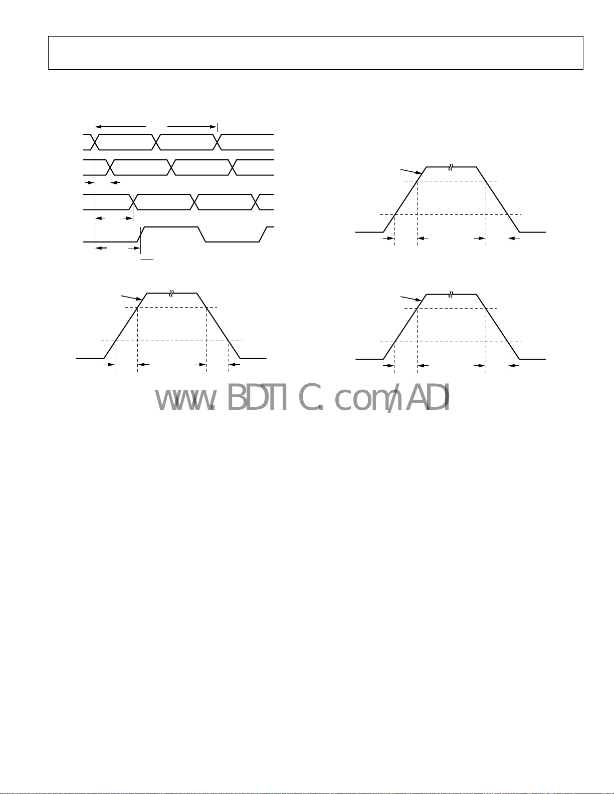
TIMING DIAGRAMS
t
CLK
CL
DIFFERENTIAL
80%
20%
t
LVDS
t
PECL
LVDS
t
CMOS
Figure 2. CLK/
DIFFERENTIAL
80%
20%
Figure 3. LVPECL Timing, Differential
CLK
to Clock Output Timing, DIV = 1
LVPECL
t
RP
t
RL
06419-060
Figure 4. LVDS Timing, Differential
SINGL E-ENDE D
80%
CMOS
10pF LOAD
20%
t
FP
06419-061
t
RC
Figure 5. CMOS Timing, Single-End
t
FL
t
FC
ed, 10 pF Load
06419-062
06419-063
Rev. 0 | Page 15 of 84
AD9516-0
www.BDTIC.com/ADI
ABSOLUTE MAXIMUM RATINGS
Table 18.
With
Parameter or Pin
VS, VS_LVPECL GND −0.3 V to +3.6 V
VCP GND −0.3 V to+5.8 V
REFIN, REFIN
REFIN
RSET GND −0.3 V to VS + 0.3 V
CPRSET GND −0.3 V to VS + 0.3 V
CLK, CLK
CLK
SCLK, SDIO, SDO, CS
OUT0, OUT0, OUT1,
, OUT2, OUT2,
OUT1
OUT3, OUT3
OUT4, OUT5, OUT5,
OUT6, OUT6
OUT7, OUT7, OUT8,
OUT8, OUT9, OUT9
SYNC
REFMON, STATUS, LD GND −0.3 V to VS + 0.3 V
Junction Temperature
Storage Temperature
Range
Lead Temperature (10 sec) 300°C
1
See Table 19 for θJA.
, OUT4,
Respec
t to Rating
GND −0.3 V to VS + 0.3 V
REFIN
GND −0.3 V to VS + 0.3 V
CLK
GND −0.3 V to VS + 0.3 V
GND −0.3 V to VS + 0.3 V
GND −0.3 V to VS + 0.3 V
GND −0.3 V to VS + 0.3 V
1
150°C
−65°C to +150°C
−3.3 V to +3.3 V
−1.2 V to +1.2 V
Stresses above those listed under Absolute Maximum Ratings
may cause permanent damage to the device. This is a stress
rating only; functional operation of the device at these or any
other conditions above those indicated in the operational
section of this specification is not implied. Exposure to absolute
maximum rating conditions for extended periods may affect
device reliability.
THERMAL RESISTANCE
Table 19.
Package Type
64-Lead LFCSP 24 °C/W
1
Thermal impedance measurements were taken on a 4-layer board in still air
in accordance with EIA/JESD51-7.
1
θ
JA
Unit
ESD CAUTION
Rev. 0 | Page 16 of 84
AD9516-0
www.BDTIC.com/ADI
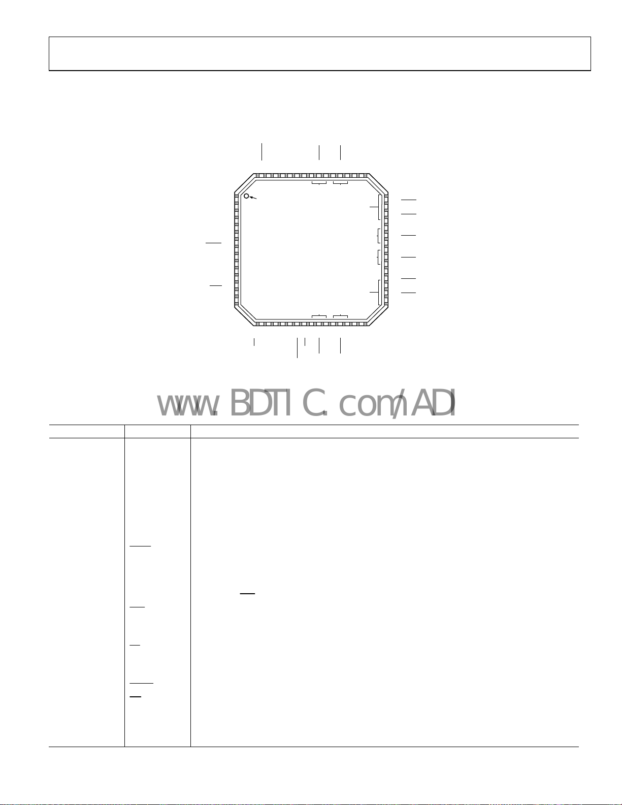
PIN CONFIGURATION AND FUNCTION DESCRIPTIONS
REFIN (REF 1)
REFIN (REF 2)
CPRSETVSVS
GND
RSETVSOUT0
OUT0
VS_LVPECL
OUT1
OUT1VSVS
646362616059585756555453525150
VS
49
VS
VCP
SYNC
CLK
CLK
SCLK
LD
CP
LF
VS
VS
NC
1
2
3
4
5
6
7
8
9
10
11
12
13
14
15
16
REFMON
STATUS
REF_SEL
BYPASS
NC = NO CONNECT
PIN 1
INDICATO R
LVPECL LVPECL
AD9516-0
TOP VIEW
(Not to Scale)
LVPECL LVPECL
171819202122232425262728293031
CS
NCNCNC
PD
SDO
SDIO
OUT4
RESET
VSVSVS
OUT4
OUT5
OUT5
VS_LVPECL
48
OUT6 (OUT6A)
47
OUT6 (OUT6B)
46
OUT7 (OUT7A)
45
LVPECL LVPECL
OUT7 (OUT7B)
44
GND
43
OUT2
42
OUT2
41
VS_LVPECL
40
OUT3
39
OUT3
38
VS
37
GND
36
OUT9 (OUT9B)
35
OUT9 (OUT9A)
34
OUT8 (OUT8B)
33
OUT8 (OUT8A)
06419-003
LVDS/CMOS
w/FINE DELAY ADJUST
LVDS/CMOS
w/FINE DELAY ADJUST
32
Figure 6. Pin Configuration
Table 20. Pin Function Descriptions
Pin No. Mnemonic Description
1, 11, 12, 30, 31,
VS 3.3 V Power Pins.
32, 38, 49, 50, 51,
57, 60, 61
2 REFMON Reference Monitor (Output). This pin has multiple selectable outputs; see Table 53 0x1B.
3 LD
4 VCP
5 CP
6 STATUS
7 REF_SEL
8
SYNC
Lock Detect (Output). This pin has multiple selectable outputs; see Table 5 3 0x1A.
Power Supply for Charge Pump (CP); VS < VCP < 5.0 V.
Charge Pump (Output). Connects to external loop filter.
Status (Output). This pin has multiple selectable outputs; see Table 53 0x17.
Reference Select. Selects REF1 (low) or REF2 (high). This pin has an internal 30 kΩ pull-down resistor.
Manual Synchronizations and Manual Holdover. This pin initiates a manual synchronization and is
also used for manual holdover. Active low. This pin has an internal 30 kΩ pull-up resistor.
9 LF
10 BYPASS
13 CLK
14
CLK
Loop Filter (Input). Connects to VCO control voltage node internally.
This pin is for bypassing the LDO to ground with a capacitor.
Along with CLK
, this is the differential input for the clock distribution section.
Along with CLK, this is the differential input for the clock distribution section.
15, 18, 19, 20 NC No Connection.
16 SCLK
17
CS
21 SDO
22 SDIO
23
24
RESET
PD
27, 41, 54 VS_LVPECL
37, 44, 59, EPAD GND
Serial Control Port Data Clock Signal.
Serial Control Port Chip Select; Active Low. This pin has an internal 30 kΩ pull-up resistor.
Serial Control Port Unidirectional Serial Data Out.
Serial Control Port Bidirectional Serial Data In/Out.
Chip Reset; Active Low. This pin has an internal 30 kΩ pull-up resistor.
Chip Power Down; Active Low. This pin has an internal 30 kΩ pull-up resistor.
Extended Voltage 2.5 V to 3.3 V LVPECL Power Pins.
Ground Pins; Includes External Paddle (EPAD).
56 OUT0 LVPECL Output; One Side of a Differential LVPECL Output.
Rev. 0 | Page 17 of 84
AD9516-0
www.BDTIC.com/ADI
Pin No. Mnemonic Description
55
53 OUT1 LVPECL Output; One Side of a Differential LVPECL Output.
52
43 OUT2 LVPECL Output; One Side of a Differential LVPECL Output.
42
40 OUT3 LVPECL Output; One Side of a Differential LVPECL Output.
39
25 OUT4 LVPECL Output; One Side of a Differential LVPECL Output.
26
28 OUT5 LVPECL Output; One Side of a Differential LVPECL Output.
29
48 OUT6 (OUT6A) LVDS/CMOS Output; One Side of a Differential LVDS Output, or a Single-Ended CMOS Output.
47
46 OUT7 (OUT7A) LVDS/CMOS Output; One Side of a Differential LVDS Output, or a Single-Ended CMOS Output.
45
33 OUT8 (OUT8A) LVDS/CMOS Output; One Side of a Differential LVDS Output, or a Single-Ended CMOS Output.
34
35 OUT9 (OUT9A) LVDS/CMOS Output; One Side of a Differential LVDS Output, or a Single-Ended CMOS Output.
36
58 RSET Resistor Connected Here Sets Internal Bias Currents. Nominal value = 4.12 kΩ.
62 CPRSET Resistor Connected Here Sets the CP Current Range. Nominal value = 5.1 kΩ.
63
64 REFIN (REF1)
OUT0
OUT1
OUT2
OUT3
OUT4
OUT5
(OUT6B)
OUT6
(OUT7B)
OUT7
(OUT8B)
OUT8
(OUT9B)
OUT9
(REF2) Along with REFIN, this is the differential input for the PLL reference. Alternatively, this pin is a
REFIN
LVPECL Output; One Side of a Differential LVPECL Output.
LVPECL Output; One Side of a Differential LVPECL Output.
LVPECL Output; One Side of a Differential LVPECL Output.
LVPECL Output; One Side of a Differential LVPECL Output.
LVPECL Output; One Side of a Differential LVPECL Output.
LVPECL Output; One Side of a Differential LVPECL Output.
LVDS/CMOS Output; One Side of a Differential LVDS Output, or a Single-Ended CMOS Output.
LVDS/CMOS Output; One Side of a Differential LVDS Output, or a Single-Ended CMOS Output.
LVDS/CMOS Output; One Side of a Differential LVDS Output, or a Single-Ended CMOS Output.
LVDS/CMOS Output; One Side of a Differential LVDS Output, or a Single-Ended CMOS Output.
single-ended input for REF2.
Along with REFIN
single-ended input for REF1.
, this is the differential input for the PLL reference. Alternatively, this pin is a
Rev. 0 | Page 18 of 84
AD9516-0
www.BDTIC.com/ADI
TYPICAL PERFORMANCE CHARACTERISTICS
300
280
260
240
220
200
180
CURRENT (mA)
160
140
120
100
0 500 1000 1500 2000 2500 3000
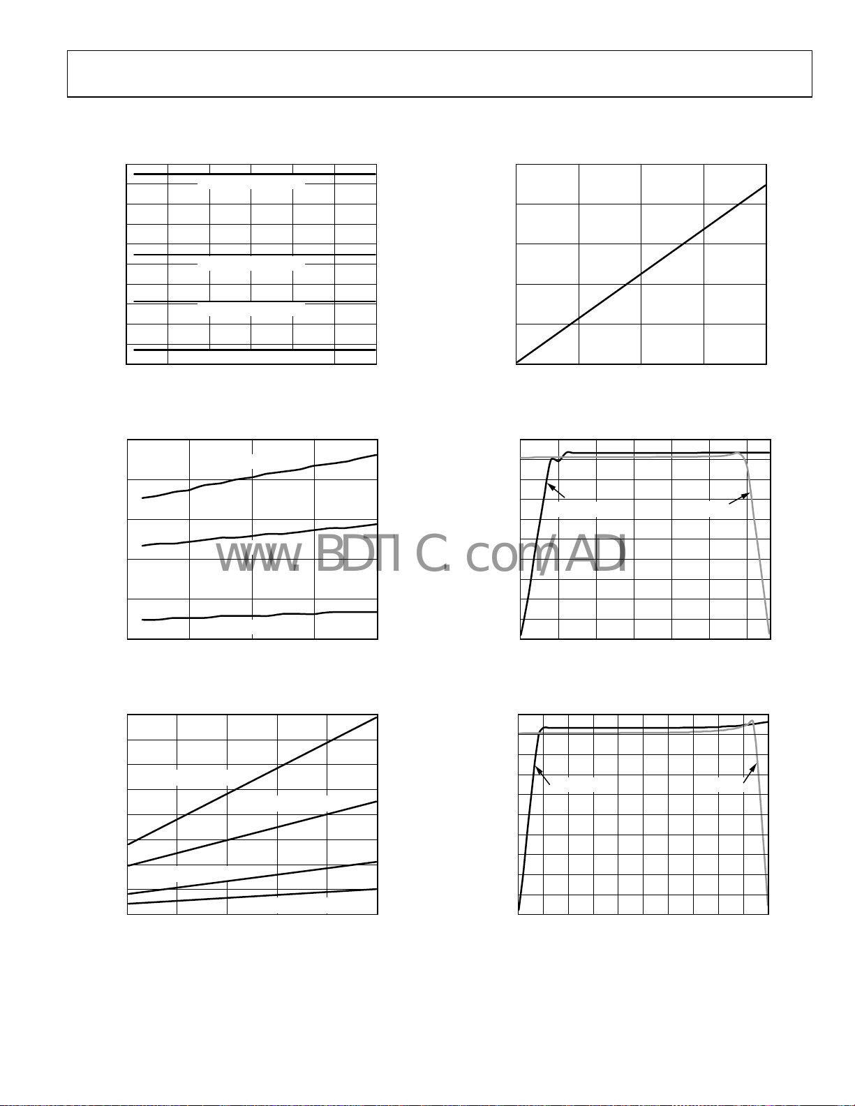
Figure 7. Current vs. Frequency, Direct
3 CHANNELS - 6 LVPECL
3 CHANNELS - 3 LVPECL
2 CHANNELS - 2 LVPECL
1 CHANNEL - 1 LVPECL
FREQUENCY (MHz)
to Output, LVPECL Outputs
06419-007
180
2 CHANNELS - 4 LVDS
160
140
120
CURRENT (mA)
100
80
0 200 400 600 800
2 CHANNELS - 2 LVDS
1 CHANNEL - 1 LVDS
FREQUENCY (MHz )
06419-008
Figure 8. Current vs. Frequency—LVDS Outputs
240
220
200
180
160
140
CURRENT (mA)
120
100
80
2 CHANNEL - 8 CMOS
2 CHANNEL - 2 CMOS
1 CHANNEL - 2 CMOS
1 CHANNEL - 1 CMOS
02
FREQUENCY (MHz )
010050
5020015
06419-009
Figure 9. Current vs. Frequency—CMOS Outputs
65
60
55
(MHz/V)
VCO
50
K
45
40
2.55 2.952.852.752.65
VCO FREQUENCY ( GHz)
Figure 10. VCO K
vs. Frequency
VCO
5.0
4.5
4.0
3.5
3.0
2.5
2.0
1.5
CURRENT FROM CP P IN (mA)
1.0
0.5
PUMP DOWN PUMP UP
0
0 0.5 1.0 1.5 2.0 2.5 3.0
VOLTAGE ON CP PIN (V)
Figure 11. Charge Pump Characteristics @ V
5.0
4.5
4.0
3.5
3.0
2.5
2.0
1.5
CURRENT FROM CP P IN (mA)
1.0
0.5
0
PUMP DOWN PUMP UP
0 0.5 1.0 1.5 2.0 3.0 4.02.5 3.5 5.04.5
VOLTAGE ON CP PIN (V)
Figure 12. Charge Pump Characteristics @ V
= 3.3 V
CP
= 5.0 V
CP
06419-010
06419-011
06419-012
Rev. 0 | Page 19 of 84
AD9516-0
–
–
www.BDTIC.com/ADI
140
–145
–150
–155
(dBc/Hz)
–160
–165
PFD PHASE NOI SE REFERRED TO PFD INPUT
–170
0.1 1 10010
PFD FREQUENCY (MHz)
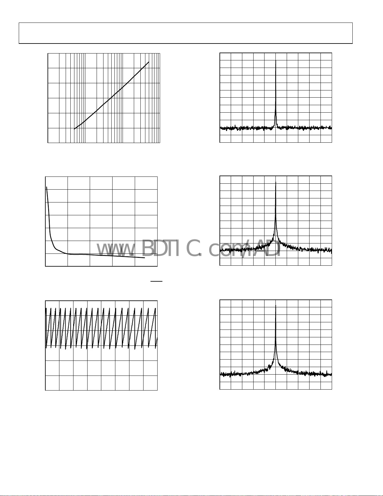
Figure 13. PFD Phase Noise Referred to PFD Input vs. PFD Frequency
210
–212
–214
–216
–218
–220
PLL FIGURE OF MERIT (dBc/ Hz)
–222
–224
02
Figure 14. PLL Figure
SLEW RATE (V/n s)
of Merit (FOM) vs. Slew Rate at REFIN/
2.1
1.9
1.7
1.5
1.3
VCO TUNING V OLTAGE (V)
1.1
0.9
2.55 2.952.902.852.802.752. 702.652.60
FREQUENCY (GHz)
Figure 15. VCO Tuning Voltage vs. Frequency
.52.01.51.00.5
REFIN
10
0
–10
–20
–30
–40
–50
–60
–70
RELATIVE P OWER (dB)
–80
–90
–100
–110
CENTER 122.88MHz SPAN 50MHz5MHz/DIV
06419-137
06419-013
Figure 16. PFD/CP Spurs; 122.88 MHz; PFD = 15.36 MHz;
LBW
= 190 kHz; I
10
0
–10
–20
–30
–40
–50
–60
–70
RELATIVE P OWER (dB)
–80
–90
–100
–110
CENTER 122.8803006MHz SPAN 1MHz100kHz/DIV
06419-136
06419-138
Figure 17. Output Spectrum, LVPECL; 122.88 MHz; PFD = 15.36 MHz;
LBW
= 190 kHz; I
10
0
–10
–20
–30
–40
–50
–60
–70
RELATIVE POWER (dB)
–80
–90
–100
–110
CENTER 122.8803006MHz SPAN 1MHz100kHz/DIV
= 4.2 mA; F
CP
= 4.2 mA; F
CP
= 2.7 GHz
VCO
= 2.7 GHz
VCO
06419-135
06419-134
Figure 18. Output Spectrum, LVDS; 122.88 MHz; PFD = 15.36 MHz;
LBW
= 190 kHz; I
= 4.2 mA; F
CP
= 2.7 GHz
VCO
Rev. 0 | Page 20 of 84
AD9516-0
www.BDTIC.com/ADI
0.4
0.2
0
–0.2
1.0
0.
0.2
6
DIFFERENTIAL OUTPUT (V)
–0.6
–1.0
02
TIME (ns)
2015105
5
06419-014
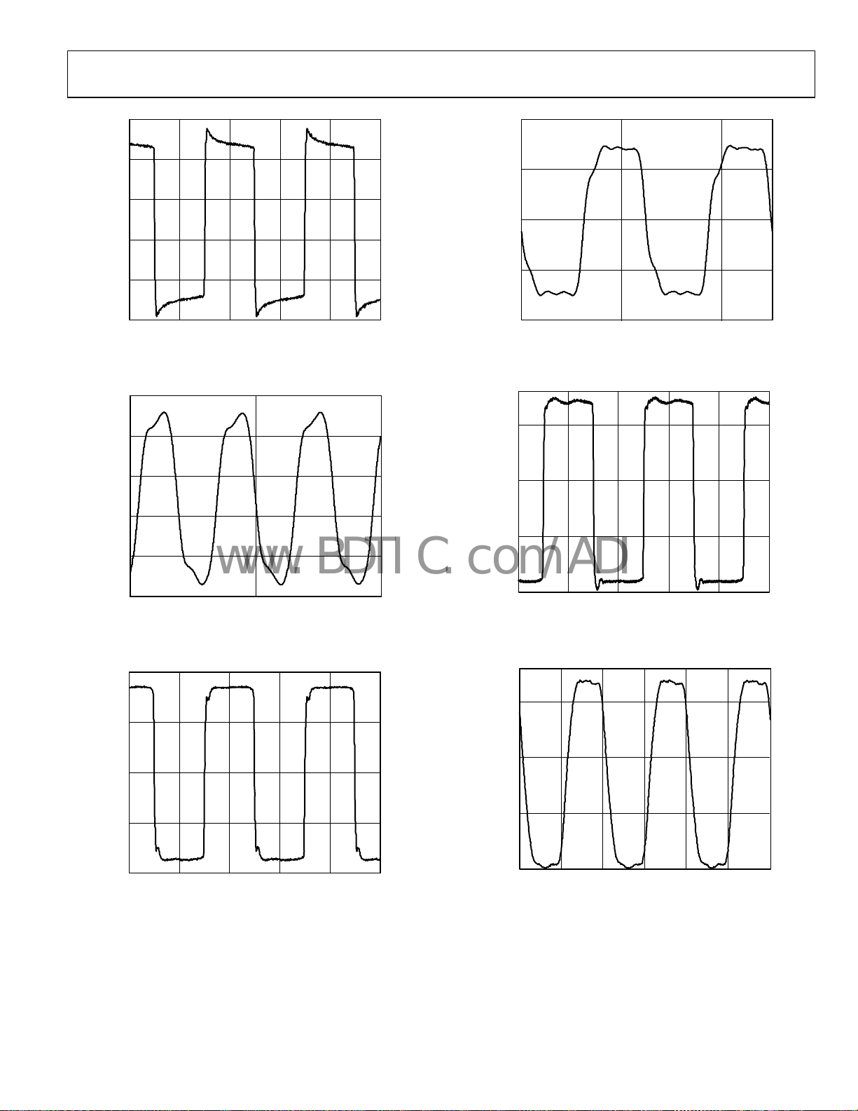
Figure 19. LVPECL Output (Differential) @ 100 MHz
–0.2
DIFFERENTIAL OUTPUT (V)
–0.4
021
Figure 22. LVDS Output (Differential) @ 800 MHz
1.0
0.6
0.2
–0.2
DIFFERENTIAL OUTPUT (V)
–0.6
–1.0
021
TIME (ns)
06419-015
2.8
1.8
0.8
DIFFERENTIAL OUTPUT (V)
–0.2
0860 1004020
Figure 20. LVPECL Output (Differential) @ 1600 MHz
0.4
TIME (ns)
TIME (ns)
Figure 23.CMOS Output @ 25 MHz
06419-017
0
06419-018
0.2
0
–0.2
DIFFERENTIAL OUTPUT (V)
–0.4
02
TIME (ns)
2015105
5
06419-016
Figure 21. LVDS Output (Differential) @ 100 MHz
Rev. 0 | Page 21 of 84
OUTPUT (V)
2.8
1.8
0.8
–0.2
086121042
Figure 24. CMOS Output @ 250 MHz
TIME (ns)
06419-019
AD9516-0
–
–
–
www.BDTIC.com/ADI
1600
1400
1200
1000
DIFFERENTIAL SWING (mV p-p)
800
0321
FREQUENCY (GHz)
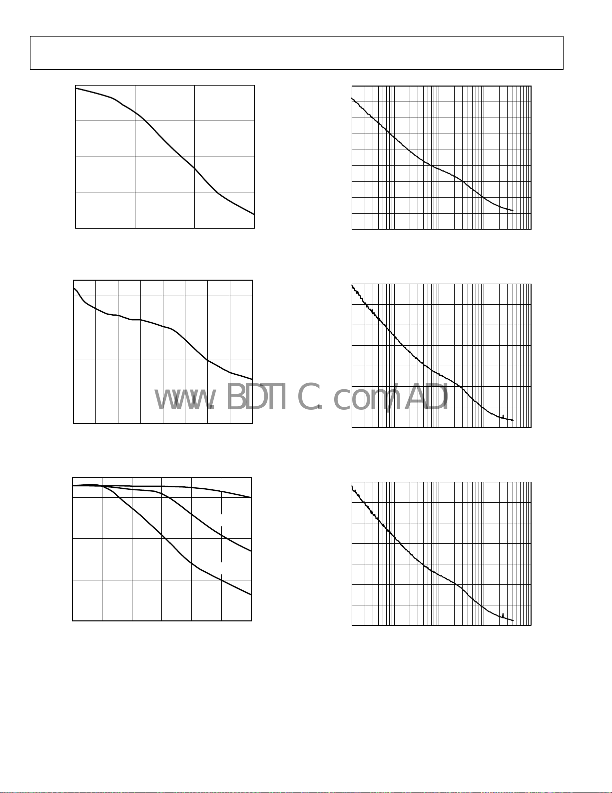
Figure 25. LVPECL Differential Swing vs. Frequency
700
600
06419-020
70
–80
–90
–100
–110
–120
–130
PHASE NOISE (dBc/Hz)
–140
–150
–160
10k 100M10M1M100k
FREQUENCY (Hz)
06419-023
Figure 28. Internal VCO Phase Noise (Absolute) Direct to LVPECL @ 2950 MHz
80
–90
–100
–110
–120
–130
DIFFERENTIAL SWING (mV p-p)
500
080070060050
FREQUENCY (MHz )
Figure 26. LVDS Differential Swing vs. Frequency
0400300200100
06419-021
PHASE NOISE (dBc/Hz)
–140
–150
10k 100M10M1M100k
Figure 29. Internal VCO Phase Noise (Absolute) Direct to LVPECL @ 2750 MHz
CL = 2pF
3
C
= 10pF
L
2
= 20pF
C
OUTPUT SWING (V)
1
0
06
OUTPUT FREQUENCY (MHz)
Figure 27. CMOS Output Swing vs. Frequency
L
500400300200100
00
and Capacitive Load
06419-133
80
–90
–100
–110
–120
–130
PHASE NOISE (dBc/Hz)
–140
–150
10k 100M10M1M100k
Figure 30. Internal VCO Phase Noise (Absolute) Direct to LVPECL @ 2550 MHz
FREQUENCY (Hz)
FREQUENCY (Hz)
06419-024
06419-025
Rev. 0 | Page 22 of 84
AD9516-0
–
–
–
–
–
–
www.BDTIC.com/ADI
120
–125
–130
110
–120
–135
–140
–145
PHASE NOISE (dBc/Hz)
–150
–155
–160
10 100M10M1M100k10k1k100
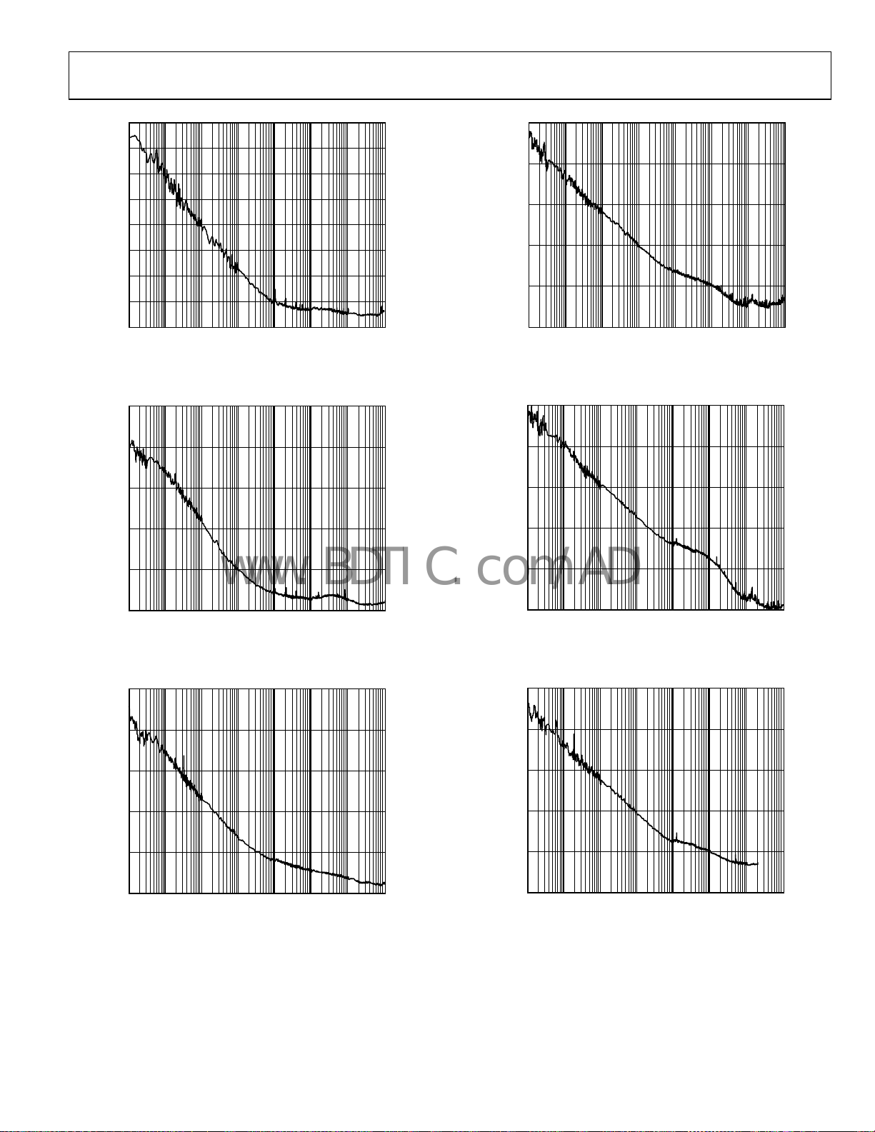
Figure 31. Phase Noise (Additive) LV
FREQUENCY (Hz)
PECL @ 245.76 MHz, Divide-by-1
110
–120
–130
–140
PHASE NOISE (dBc/Hz)
–150
–160
10 100M10M1M100k10k1k100
FREQUENCY (Hz)
Figure 32. Phase Noise (Additive) LVPECL @ 200 M
100
Hz, Divide-by-5
–130
–140
PHASE NOISE (dBc/Hz)
–150
–160
10 100M1k 10k 100k 1M 10M100
06419-026
Figure 34. Phase Noise (Additive) LVD
FREQUENCY (Hz)
S @ 200 MHz, Divide-by-1
06419-142
100
–110
–120
–130
PHASE NOISE (dBc/Hz)
–140
–150
10 100M10M1M100k10k1k100
06419-027
Figure 35. Phase Noise (Additive) LVD
FREQUENCY (Hz)
S @ 800 MHz, Divide-by-2
06419-130
120
–110
–120
–130
PHASE NOISE (dBc/Hz)
–140
–150
10 100M10M1M100k10k1k100
Figure 33. Phase Noise (Additive) LVPECL @ 1600 MHz, D
FREQUENCY (Hz)
ivide-by-1
06419-128
Rev. 0 | Page 23 of 84
–130
–140
–150
PHASE NOISE (dBc/Hz)
–160
–170
10 100M10M1M100k10k1k100
FREQUENCY (Hz)
Figure 36. Phase Noise (Additive) CM
OS @ 50 MHz, Divide-by-20
06419-131
AD9516-0
–
–
–
–
www.BDTIC.com/ADI
100
90
–110
–120
–130
–140
PHASE NOISE (dBc/Hz)
–150
–160
10 100M10M1M100k10k1k100
FREQUENCY (Hz)
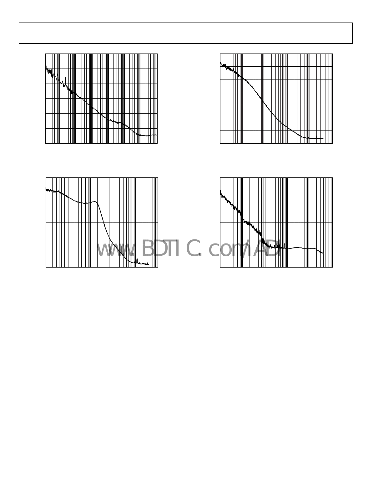
Figure 37. Phase Noise (Additive) CM
120
–130
–140
PHASE NOISE (dBc/Hz)
–150
OS @ 250 MHz, Divide-by-4
–100
–110
–120
–130
–140
PHASE NOISE (dBc/Hz)
–150
–160
1k 100M10M1M100k10k
06419-132
FREQUENCY (Hz)
06419-139
Figure 39. Phase Noise (Absolute) Clock Cleanup; Internal VCO @ 2.8 GHz;
P
FD = 19.44 MHz; LBW = 12.8 kHz; LVPECL Output = 155.52 MHz
120
–130
–140
PHASE NOISE (dBc/Hz)
–150
–160
1k 100M10M1M100k10k
FREQUENCY (Hz)
Figure 38. Phase Noise (Absolute) Clock Generation; Internal VCO @ 2.7 GHz;
P
FD = 15.36 MHz; LBW = 110 kHz; LVPECL Output = 122.88 MHz
–160
1k 100M10M1M100k10k
06419-141
Figure 40. Phase Noise (Absolute), Ex
FREQUENCY (Hz)
ternal VCXO (Toyocom TCO-2112)
06419-140
@ 245.76 MHz; PFD = 15.36 MHz; LBW = 250 Hz; LVPECL Output = 245.76 MHz
Rev. 0 | Page 24 of 84

AD9516-0
www.BDTIC.com/ADI
TERMINOLOGY
Phase Jitter and Phase Noise
An ideal sine wave can be thought of as having a continuous
nd even progression of phase with time from 0° to 360° for
a
each cycle. Actual signals, however, display a certain amount
of variation from ideal phase progression over time. This
phenomenon is called phase jitter. Although many causes can
contribute to phase jitter, one major cause is random noise,
which is characterized statistically as being Gaussian (normal)
in distribution.
This phase jitter leads to a spreading out of the energy of the
sin
e wave in the frequency domain, producing a continuous
power spectrum. This power spectrum is usually reported as a
series of values whose units are dBc/Hz at a given offset in
frequency from the sine wave (carrier). The value is a ratio
(expressed in dB) of the power contained within a 1 Hz
bandwidth with respect to the power at the carrier frequency.
For each measurement, the offset from the carrier frequency is
also given.
It is meaningful to integrate the total power contained within
ome interval of offset frequencies (for example, 10 kHz to
s
10 MHz). This is called the integrated phase noise over that
frequency offset interval and can be readily related to the time
jitter due to the phase noise within that offset frequency interval.
Phase noise has a detrimental effect on the performance of
Cs, DACs, and RF mixers. It lowers the achievable dynamic
AD
range of the converters and mixers, although they are affected
in somewhat different ways.
Time Jitter
Phase noise is a frequency domain phenomenon. In the time
do
main, the same effect is exhibited as time jitter. When
observing a sine wave, the time of successive zero crossings
varies. In a square wave, the time jitter is a displacement of the
edges from their ideal (regular) times of occurrence. In both
cases, the variations in timing from the ideal are the time jitter.
Because these variations are random in nature, the time jitter is
specified in units of seconds root mean square (rms) or 1 sigma
of the Gaussian distribution.
Time jitter that occurs on a sampling clock for a DAC or an
C decreases the signal-to-noise ratio (SNR) and dynamic
AD
range of the converter. A sampling clock with the lowest possible
jitter provides the highest performance from a given converter.
Additive Phase Noise
Additive phase noise is the amount of phase noise that is
ttributable to the device or subsystem being measured. The
a
phase noise of any external oscillators or clock sources are
subtracted. This makes it possible to predict the degree to which
the device impacts the total system phase noise when used in
conjunction with the various oscillators and clock sources, each
of which contribute their own phase noise to the total. In many
cases, the phase noise of one element dominates the system
phase noise. When there are multiple contributors to phase
noise, the total is the square root of the sum of squares of the
individual contributors.
Additive Time Jitter
Additive time jitter is the amount of time jitter that is
ttributable to the device or subsystem being measured. The
a
time jitter of any external oscillators or clock sources are subtracted.
This makes it possible to predict the degree to which the device
impacts the total system time jitter when used in conjunction with
the various oscillators and clock sources, each of which
contribute their own time jitter to the total. In many cases, the
time jitter of the external oscillators and clock sources dominates
the system time jitter.
Rev. 0 | Page 25 of 84
AD9516-0
V
www.BDTIC.com/ADI
DETAILED BLOCK DIAGRAM
REFIN (REF1)
REFIN (REF2)
BYPASS
CLK
CLK
SYNC
RESET
SCLK
SDIO
SDO
REF1
REF2
LF
PD
CS
REF_ SEL CPRSETVCP
REFERENCE
SWITCHOVER
STATUS
STATUS
LOW DROPOUT
REGULATOR ( LDO)
VCO
DIGITAL
LOGIC
SERIAL
CONTROL
PORT
S GND RSET
DISTRIBUTI ON
REFERENCE
R
DIVIDER
VCO STATUS
P, P + 1
PRESCALER
DIVIDE BY
2, 3, 4, 5, OR 6
01
N DIVIDER
A/B
COUNTER S
REFMON
PROGRAMMABLE
R DELAY
PROGRAMMABLE
N DELAY
DIVIDE BY
1 TO 32
DIVIDE BY
1 TO 32
DIVIDE BY
1 TO 32
LOCK
DETECT
PHASE
FREQUENCY
DETECTOR
PLL
REFERENCE
CHARGE
PUMP
HOLD
LVPECL
LVPECL
LVPECL
LD
CP
STATUS
OUT0
OUT0
OUT1
OUT1
OUT2
OUT2
OUT3
OUT3
OUT4
OUT4
OUT5
OUT5
AD9516-0
DIVIDE BY
1 TO 32
DIVIDE BY
1 TO 32
DIVIDE BY
1 TO 32
DIVIDE BY
1 TO 32
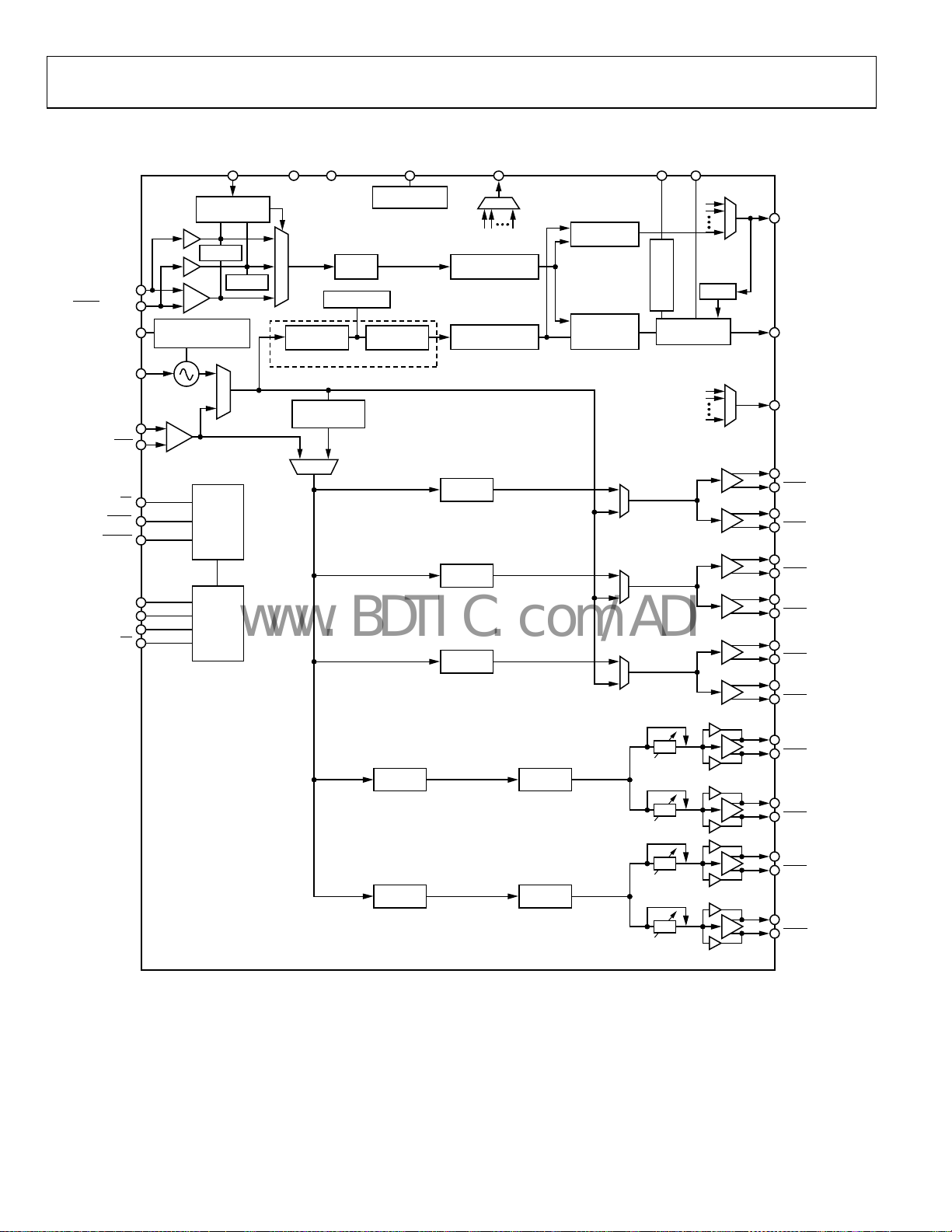
Figure 41. Detailed Block Diagram
Rev. 0 | Page 26 of 84
ΔT
ΔT
ΔT
ΔT
LVDS/CMOS
LVDS/CMOS
OUT6 (OUT6A)
OUT6 (OUT6B)
OUT7 (OUT7A)
OUT7 (OUT7B)
OUT8 (OUT8A)
OUT8 (OUT8B)
OUT9 (OUT9A)
OUT9 (OUT9B)
6419-002
 Loading...