800 MHz Clock Distribution IC, PLL Core,
V
Preliminary Technical Data
FEATURES
Low phase noise phase-locked loop core
Reference input frequencies to 250 MHz
Programmable dual-modulus prescaler
Programmable charge pump (CP) current
Separate CP supply (VCP) extends tuning range
Two 1.5 GHz, differential clock inputs
5 programmable dividers, 1 to 32, all integers
Phase select for output-to-output coarse delay adjust
3 independent 800 MHz LVPECL outputs
Additive output jitter 225 fs rms
2 independent 800 MHz/250 MHz LVDS/CMOS clock outputs
Additive output jitter 275 fs rms
Fine delay adjust on 1 output, 6-bit delay word
4-wire or 3-wire serial control port
Space-saving, 48-lead LFCSP
APPLICATIONS
Low jitter, low phase noise clock distribution
Clocking high speed ADCs, DACs, DDS, DDC, DUC, MxFEs
High performance wireless transceivers
High performance instrumentation
Broadband infrastructure
GENERAL DESCRIPTION
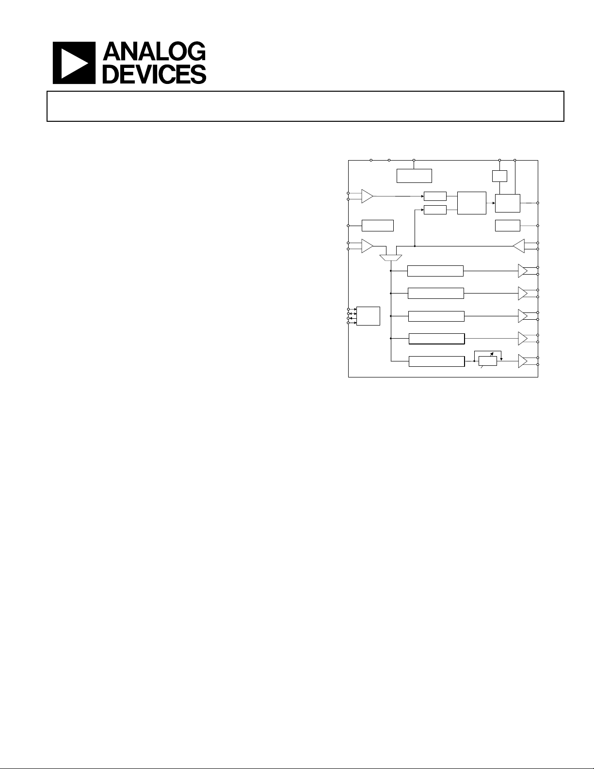
The AD9511 provides a multi-output clock distribution
function along with an on-chip PLL core. The design
emphasizes low jitter and phase noise in order to maximize data
converter performance. Other applications with demanding
phase noise and jitter requirements also benefit from this part.
The PLL section consists of a programmable reference divider
(R); a low noise phase frequency detector (PFD); a precision
charge pump (CP); and a programmable feedback divider (N).
By connecting an external VCXO or VCO to the CLK2/CLK2B
pins, frequencies up to 1.5 GHz may be synchronized to the
input reference.
There are five independent clock outputs. Three outputs are
LVPECL, and two are selectable as either LVDS or CMOS levels.
The LVPECL and LVDS outputs operate to 800 MHz, and the
CMOS outputs operate to 250 MHz.
Dividers, Delay Adjust, Five Outputs
AD9511
FUNCTIONAL BLOCK DIAGRAM
CP
REFIN
REFINB
FUNCTION
CLK1
CLK1B
SCLK
SDIO
SDO
CSB
VS GND
SYNCB,
RESETB PDB
SERIAL
CONTROL
PORT
RSET
DISTRIBUTION
REF
R
DIVIDER
N
DIVIDER
PROGRAMMABLE DIVIDERS
& PHASE ADJUST
/1,/2,/3... /31,/32
/1,/2,/3... /31,/32
/1,/2,/3... /31,/32
/1,/2,/3... /31,/32
/1,/2,/3... /31,/32
AD9511
F
R
DETECTOR
Figure 1.
Each output has a programmable divider that may be bypassed
or set to divide by any integer up to 32. The phase of one clock
output relative to another clock output may be varied by means
of a divider phase select function, which serves as a coarse
timing adjustment. One of the LVDS/CMOS outputs also
features a programmable delay element with a range of up to
10 ns of delay. This fine tuning delay block has 6-bit resolution,
giving 64 possible delays from which to choose.
The AD9511 is ideally suited for data converter clocking
applications where maximum converter performance is
achieved by encode signals with subpicosecond jitter.
The AD9511 is available in a 48-lead LFCSP and may be
operated from a single 3.3 V supply. An external VCO that
requires an extended voltage range may be accommodated by
connecting the charge pump supply (VCP) to 5.5 V. The
temperature range is −40°C to +85°C.
PHASE
E
Q
N
E
U
DELAY ADJUST
CPRSET
PLL
REF
CHARGE
C
Y
PUMP
PLL
SETTINGS
∆T
LVPECL
LVPECL
LVPECL
LVDS/CMOS
LVDS/CMOS
CP
STATUS
CLK2
CLK2B
OUT0
OUT0B
OUT1
OUT1B
OUT2
OUT2B
OUT3
OUT3B
OUT4
OUT4B
Rev. PrA
Information furnished by Analog Devices is believed to be accurate and reliable.
However, no responsibility is assumed by Analog Devices for its use, nor for any
infringements of patents or other rights of third parties that may result from its use.
Specifications subject to change without notice. No license is granted by implication
or otherwise under any patent or patent rights of Analog Devices. Trademarks and
registered trademarks are the property of their respective owners.
One Technology Way, P.O. Box 9106, Norwood, MA 02062-9106, U.S.A.
Tel: 781.329.4700
Fax: 781.326.8703 © 2004 Analog Devices, Inc. All rights reserved.
www.analog.com

AD9511 Preliminary Technical Data
PR05286-0-11/04(PrA)
PIN CONFIGURATION
T
E
S
T
D
E
R
N
S
P
V
C
48
S
R
G
47
46
D
N
S
V
G
45
44
43
B
0
0
T
T
U
U
O
O
42
41
S
S
V
V
40
39
D
D
N
N
G
G
38
37
R
E
R
C
C
C
U
F
C
N
1
F
E
N
I
2
F
B
N
I
3
S
V
4
V
P
C
C
P
5
V
S
6
L
C
2
K
7
8
L
K
2
B
S
V
9
L
1
K
10
11
L
K
1
B
T
O
I
N
12
pin 1
indicator
AD9511
Top View
(Not to scale)
48-leadLFCSP7 x 7 x 0.85
13
14
15
16
17
18
S
K
U
T
A
T
S
O
L
I
C
D
S
S
B
O
S
D
C
S
19
S
D
V
N
G
21
20
B
2
T
U
O
22
23
24
2
S
T
V
U
O
D
S
N
V
G
36
35
34
33
32
31
30
29
28
27
26
25
S
V
OUT3
OUT3B
S
V
S
V
U
O
O
U
V
S
V
S
O
U
O
U
V
S
T
T
T
T1B
4
B
4
1
Figure 2.
Note that the exposed paddle on this package is an electrical connection as well as a thermal enhancement. For the device to
function properly, the paddle must be attached to ground, GND.
© 2004 Analog Devices, Inc. All rights reserved. Trademarks and
registered trademarks are the property of their respective companies.
Rev. PrA | Page 2 of 2
 Loading...