

Digitally Programmable
a
FEATURES
Single +5 V Supply
TTL and CMOS Compatible
10 ps Delay Resolution
2.5 ns to 10 ms Full-Scale Range
Maximum Trigger Rate 50 MHz
MIL-STD-883-Compliant Versions Available
APPLICATIONS
Disk Drive Deskewing
Data Communications
Test Equipment
Radar I & Q Matching
GENERAL DESCRIPTION
The AD9501 is a digitally programmable delay generator which
provides programmed time delays of an input pulse. Operating
from a single +5 V supply, the AD9501 is TTL- or CMOScompatible, and is capable of providing accurate timing adjustments with resolutions as low as 10 ps. Its accuracy and
programmability make it ideal for use in data deskewing and
pulse delay applications, as well as clock timing adjustments.
Full-scale delay range is set by the combination of an external
resistor and capacitor, and can range from 2.5 ns to 10 µs for a
Delay Generator
AD9501
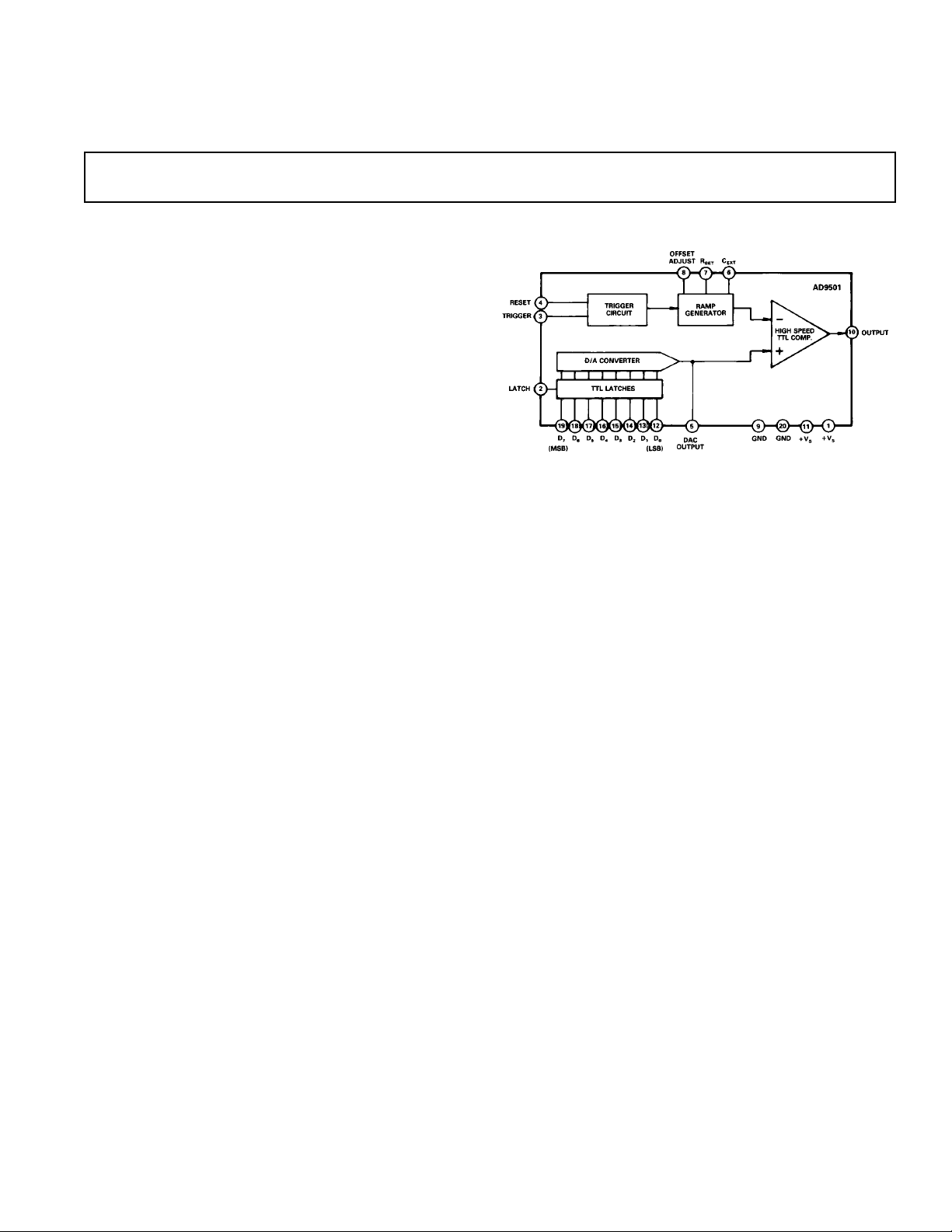
FUNCTIONAL BLOCK DIAGRAM
single AD9501. An eight-bit digital word selects a time delay
within the full-scale range. When triggered by the rising edge of
an input pulse, the output of the AD9501 will be delayed by an
amount equal to the selected time delay (t
propagation delay (t
The AD9501 is available for a commercial temperature range of
0°C to +70°C in a 20-pin plastic DIP, 20-pin ceramic DIP, and
a 20-lead plastic leaded chip carrier (PLCC). Devices fully
compliant to MIL-STD-883 are available in ceramic DIPs.
Refer to the Analog Devices Military Products Databook or current
AD9501/883B data sheet for detailed specifications.
PD
).
) plus an inherent
D
REV. A
Information furnished by Analog Devices is believed to be accurate and
reliable. However, no responsibility is assumed by Analog Devices for its
use, nor for any infringements of patents or other rights of third parties
which may result from its use. No license is granted by implication or
otherwise under any patent or patent rights of Analog Devices.
One Technology Way, P.O. Box 9106, Norwood, MA 02062-9106, U.S.A.
Tel: 617/329-4700 Fax: 617/326-8703

AD9501–SPECIFICA TIONS
ABSOLUTE MAXIMUM RATINGS
Positive Supply Voltage . . . . . . . . . . . . . . . . . . . . . . . . . . +7 V
Digital Input Voltage Range . . . . . . . . . . . . . . . –0.5 V to +V
Trigger/Reset Input Volt. Range . . . . . . . . . . . . –0.5 V to +V
Minimum R
. . . . . . . . . . . . . . . . . . . . . . . . . . . . . . . . 30 Ω
SET
Digital Output Current (Sourcing) . . . . . . . . . . . . . . . 10 mA
1
Operating Temperature Range
AD9501JN/JP/JQ . . . . . . . . . . . . . . . . . . . . . . 0°C to +70°C
S
S
AD9501SQ . . . . . . . . . . . . . . . . . . . . . . . –55°C to +125°C
Storage Temperature Range . . . . . . . . . . . . –65°C to +150°C
Junction Temperature
2
. . . . . . . . . . . . . . . . . . . . . . . +175°C
Lead Soldering Temperature (10 sec) . . . . . . . . . . . . +300°C
Digital Output Current (Sinking) . . . . . . . . . . . . . . . . 50 mA
ELECTRICAL CHARACTERISTICS
[+VS = +5 V; C
device output connected to Pin 4 RESET input unless otherwise noted]
= Open; R
EXT
= 3090 Ω (Full-Scale Range =100 ns); Pin 8 grounded; and
SET
08C to +708C –558C to +1258C
Test AD9501JN/JP/JQ AD9501SQ
Parameter Temp Level Min Typ Max Min Typ Max Units
RESOLUTION 8 8 Bits
ACCURACY
Differential Nonlinearity +25°C I 0.5 0.5 LSB
Integral Nonlinearity +25°C I 1 1 LSB
Monotonicity +25°C I Guaranteed Guaranteed
DIGITAL INPUTS
Latch Input “1” Voltage Full VI 2.0 2.3 V
Latch Input “0” Voltage Full VI 0.8 0.8 V
Logic “1” Voltage Full VI 2.0 2.0 V
Logic “0” Voltage Full VI 0.8 0.8 V
Logic “1” Current Full VI 60 60 µA
Logic “0” Current Full VI 3 3 µA
Digital Input Capacitance +25°C IV 5.5 5.5 pF
Data Setup Time (t
Data Hold Time (t
Latch Pulse Width (t
3
)
S
4
)
H
) +25°C V 3.5 3.5 ns
L
+25°C V 2.5 2.5 ns
+25°C V 2.5 2.5 ns
Reset/Trigger Pulse Width (tR, tT) +25°CV 2 2 ns
DYNAMIC PERFORMANCE
Maximum Trigger Rate
Minimum Propagation Delay (t
Propagation Delay Tempco
5
PD
7
+25°CIV 1822 1822 MHz
6
)
+25°C I 25 30 25 30 ns
Full V 25 25 ps/°C
Full-Scale Range Tempco Full V 36 36 ps/°C
Delay Uncertainty +25°C V 53 53 ps
Reset Propagation Delay (t
Reset-to-Trigger Holdoff (t
Trigger-to-Reset Holdoff (t
Minimum Output Pulse Width
Output Rise Time
Output Fall Time
DAC Settling Time (t
12
12
LD
Linear Ramp Settling Time (t
8
RD
THO
RHO
)
9
)
10
)
11
+25°C I 14.5 17.5 14.5 17.5 ns
+25°C V 4.5 4.5 ns
+25°C V 19 19 ns
+25°C V 7.5 7.5 ns
+25°C I 2.3 3.5 2.3 3.5 ns
13
)
LRS
+25°C I 1.0 2.0 1.0 2.0 ns
+25°C V 30 30 ns
14
)
+25°C V 20 20 ns
DIGITAL OUTPUT
Logic “1” Voltage (Source 1 mA) Full VI 2.4 2.4 V
Logic “0” Voltage (Sink 4 mA) Full VI 0.24 0.4 0.24 0.5 V
POWER SUPPLY
15
Positive Supply Current (+5.0 V) Full VI 69.5 83 69.5 83 mA
Power Dissipation Full VI 415 415 mW
Power Supply Rejection Ratio
16
Full-Scale Range Sensitivity +25°C I 0.7 2.0 0.7 2.0 ns/V
Minimum Prop Delay Sensitivity +25°C I 0.45 1.7 0.45 1.7 ns/V
–2–
REV. A
AD9501
NOTES
1
Absolute maximum ratings are limiting values, to be applied individually, and beyond which the serviceability of the circuit may be impaired. Functional operability
is not necessarily implied. Exposure to absolute maximum rating conditions for an extended period of time may affect device reliability.
2
Typical thermal impedances: 20-lead plastic leaded chip carrier θJA= 73°C/W; θJC= 29°C/W. 20-pin ceramic DIP θJA= 65°C/W; θJC= 20°C/W. 20-pin plastic DIP
θJA= 65°C/W; θJC= 26°C/W.
3
Digital data inputs must remain stable for the specified time prior to the positive transition of the LATCH signal.
4
Digital data inputs must remain stable for the specified time after the positive transition of the LATCH signal.
5
Programmed delay (tD) = 0 ns. Maximum self-resetting trigger rate is limited to 6.9 MHz with 100 ns programmed delay. If tD= 0 ns and external RESET signal is
used, maximum trigger rate is 23 MHz.
6
Programmed delay (tD) = 0 ns. In operation, any programmed delays are in addition to the minimum propagation delay (tPD).
7
Programmed delay (tD) = 0 ns. [Minimum propagation delay (tPD)].
8
Measured from 50% transition point of the RESET signal input to the 50% transition point of the falling edge of the output.
9
Minimum time from the falling edge of RESET to the triggering input to insure valid output pulse, using external RESET pulse.
10
Minimum time from triggering event to rising edge of RESET to insure valid output event, using external RESET pulse. Extends to 125 ns when programmed delay
is 100 ns.
11
When self-resetting with a full-scale programmed delay.
12
Measured from +0.4 V to +2.4 V; source = 1 mA; sink = 4 mA.
13
Measured from the data input to the time when the AD9501 becomes 8-bit accurate, after a full-scale change in the program delay data word.
14
Measured from the RESET input to the time when the AD9501 becomes 8-bit accurate, after a full-scale programmed delay.
15
Supply voltage should remain stable within ±5% for normal operation.
16
Measured at +VS = +5.0 V ± 5%; specification shown is for worst case.
Specifications subject to change without notice.
EXPLANATION OF TEST LEVELS
Test Level
I – 100% production tested.
II – 100% production tested at +25°C, and sample tested at specified
temperatures.
III – Sample tested only.
IV – Parameter is guaranteed by design and characterization testing.
V – Parameter is a typical value only.
VI – All devices are 100% production tested at +25°C. 100% production
tested at temperature extremes for extended temperature devices;
sample tested at temperature extremes for commercial/industrial
devices.
ORDERING GUIDE
Device Temperature Description Option*
AD9501JN 0°C to +70°C 20-Pin Plastic DIP N-20
AD9501JP 0°C to +70°C 20-Lead PLCC P-20A
AD9501JQ 0°C to +70°C 20-Pin Ceramic DIP Q-20
AD9501SQ –55°C to +125°C 20-Pin Ceramic DIP Q-20
*N = Plastic DIP; P = Plastic Leaded Chip Carrier; Q = Cerdip.
DIE LAYOUT AND MECHANICAL INFORMATION
Package
MECHANICAL INFORMATION
Die Dimensions . . . . . . . . . . . . . . . . . . 89 × 153 × 15 (±2) mils
Pad Dimensions . . . . . . . . . . . . . . . . . . . . . . . . . . . . .4 × 4 mils
Metalization . . . . . . . . . . . . . . . . . . . . . . . . . . . . . . . Aluminum
Backing . . . . . . . . . . . . . . . . . . . . . . . . . . . . . . . . . . . . . . None
Substrate Potential . . . . . . . . . . . . . . . . . . . . . . . . . . . . Ground
Passivation . . . . . . . . . . . . . . . . . . . . . . . . . . . . . . . . Oxynitride
Die Attach . . . . . . . . . . . . . . . . . . . . . . . . . . . . . .Gold Eutectic
Bond Wire . . . . . . . . 1.25 mil, Aluminum; Ultrasonic Bonding
or 1 mil, Gold; Gold Ball Bonding
REV. A
–3–
AD9501
WARNING!
ESD SENSITIVE DEVICE
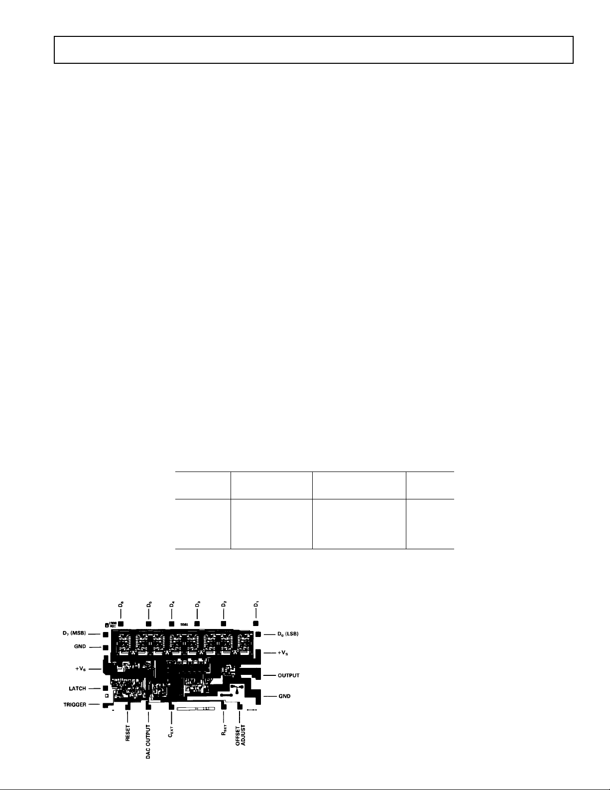
Pin No. Name Function
AD9501 PIN DESCRIPTIONS
1+V
S
2 LATCH TTL/CMOS register control line. Logic HIGH latches input data D
Positive voltage supply; nominally +5 V.
. Register is
0–D7
transparent for logic LOW.
3 TRIGGER TTL/CMOS-compatible input. Rising edge triggers the internal ramp generator, and begins
the delay cycle.
4 RESET TTL/CMOS-compatible input. Logic HIGH resets the ramp voltage and OUTPUT.
5 DAC OUTPUT Output voltage of the internal digital-to-analog converter.
6C
7R
EXT
SET
8 OFFSET ADJUST Normally connected to GROUND. Can be used to adjust minimum propagation delay (t
Optional external capacitor connected to +VS; used with R
to determine full-scale delay range (t
DFS
).
External resistor to ground, used to determine full-scale delay range (t
and 8.5 pF internal capacitor
SET
DFS
).
);
PD
see Theory of Operation text.
9 GROUND Circuit ground return.
10 OUTPUT TTL-compatible delayed output pulse.
11 +V
12-19 D
S
0–D7
Positive voltage supply; nominally +5 V.
TTL/CMOS-compatible inputs, used to set the programmed delay of the AD9501 delayed
output. D
is LSB and D7 is MSB.
0
20 GROUND Circuit ground return.
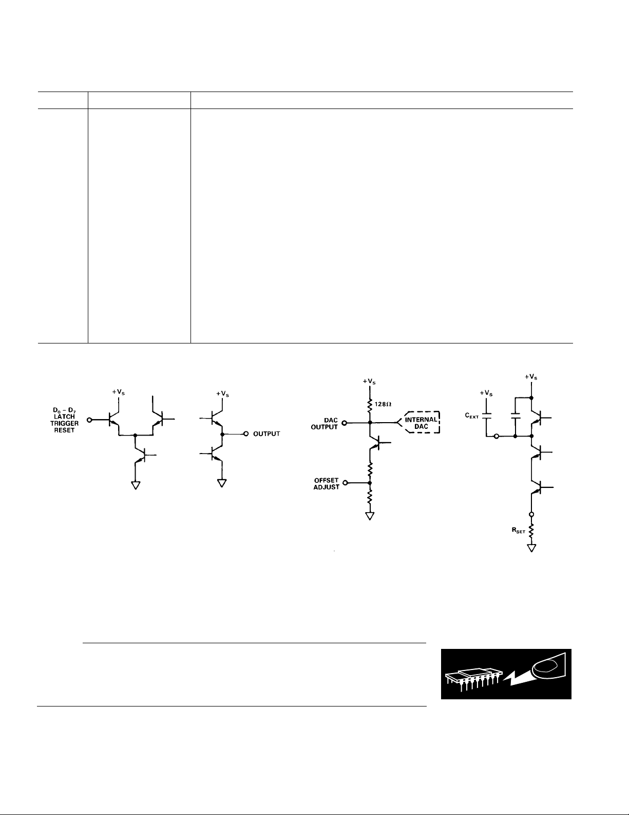
AD9501 Equivalent Circuits
CAUTION
ESD (electrostatic discharge) sensitive device. Electrostatic charges as high as 4000 V readily
accumulate on the human body and test equipment and can discharge without detection.
Although the AD9501 features proprietary ESD protection circuitry, permanent damage may
occur on devices subjected to high energy electrostatic discharges. Therefore, proper ESD
precautions are recommended to avoid performance degradation or loss of functionality.
–4–
REV. A

AD9501
THEORY OF OPERATION
The AD9501 is a digitally programmable delay device. Its
function is to provide a precise incremental delay between input
and output, proportional to an 8-bit digital word applied to its
delay control port. Incremental delay resolution is 10 ps at the
minimum full-scale range of 2.5 ns. Digital delay data inputs,
latch, trigger and reset are all TTL/CMOS compatible. Output
is TTL-compatible.
Refer to the block diagram of the AD9501.
Inside the unit, there are three main subcircuits: a linear ramp
generator, an 8-bit digital-to-analog converter (DAC) and a
voltage comparator. The rising edge of the input (TRIGGER)
pulse initiates the delay cycle by triggering the ramp generator.
The voltage comparator monitors the ramp voltage and switches
the delayed output (Pin 10) HIGH when the ramp voltage
crosses the threshold set by the DAC output voltage. The DAC
threshold voltage is programmed by the user with digital inputs.
Figure 1, the AD9501 Internal Timing diagram, illustrates in
detail how the delay is determined. Minimum Delay (t
) is the
PD
sum of Trigger Circuit delay, Ramp Generator delay, and
Comparator delay.
The Trigger Circuit delay and Comparator delay are fixed;
Ramp Generator delay is a variable affected by the rate of
change of the linear ramp and (to a lesser degree) the value of
the offset voltage described below.
Maximum Delay is the sum of Minimum Delay (t
Scale Program Delay (t
DFS
).
) and Full-
PD
Ramp Generator delay is the time required for the ramp to slew
from its reset voltage to the most positive DAC reference
voltage (00
). The difference in these two voltages is nominally
H
18 mV (with OFFSET ADJUST open) or 34 mV (OFFSET
ADJUST grounded).
REV. A
Figure 1. AD9501 Internal Timing
–5–

AD9501
Offset between the two levels is necessary for three reasons.
First, offset allows the ramp to reset and settle without reentering the voltage range of the DAC. Second, the DAC may
overshoot as it switches to its most positive value (00
); this
H
could lead to false output pulses if there were no offset between
the ramp reset voltage and the upper reference. Overshoot on
the ramp could also lead to false outputs without the offset.
Finally, the ramp is slightly nonlinear for a short interval when it
is first started; the offset shifts the most positive DAC level
below this nonlinear region and maintains ramp linearity for
short programmed delay settings.
Pin 8 of the AD9501 is called OFFSET ADJUST (see block
diagram) and allows the user to control the amount of offset
separating the initial ramp voltage and the most positive DAC
reference. This, in turn, causes the Ramp Generator delay to
vary.
Figure 2 shows differences in timing which occur if OFFSET
ADJUST Pin 8 is grounded or open. The variable Ramp
Generator delay is the major component of the three
components which comprise Minimum Delay (t
PD
) and,
therefore, is affected by the connection to Pin 8.
It is preferable to ground Pin 8 because the smaller offset that
results from leaving it open increases the possibility of false output pulses. When grounding the pin, it should be grounded
directly or connected to ground through a resistor or potentiometer with a value of 10 kΩ or less.
Caution is urged when using resistance in series with Pin 8. The
possibility of false output pulses, as discussed above, is increased under these circumstances. Using resistance in series
with Pin 8 is recommended only when matching minimum delays between two or more AD9501 devices; it is not recommended if using a single AD9501. Changing the resistance
between Pin 8 and ground from zero to 10 kΩ varies the Ramp
Generator Delay by approximately 35%.
The Full-Scale Delay Range (t
) can be calculated from the
DFS
equation:
(t
)= R
DFS
Whenever Full-Scale Delay Range is 326 ns or less, C
be left open. Additional capacitance and/or larger values of R
SET
×(C
+8.5 pF)× 3.84
EXT
EXT
should
SET
increase the Linear Ramp Settling Time, which reduces the
maximum trigger rate. When delays longer than 326 ns are
required, up to 500 pF can be connected from C
R
should be selected in the range from 50 Ω to 10 kΩ. Graph
SET
EXT
to +VS.
1 shows typical Full-Scale Delay Ranges for various values of
R
SET
and C
EXT
.
Figure 2. AD9501 Minimum Delay (tPD) vs. Full-Scale Delay Range (t
–6–
DFS
)
REV. A

AD9501
Ramp charging current and DAC full-scale current are slaved
together in the AD9501 to minimize delay drift over temperature. To preserve the unit’s low drift performance, both R
and C
should have low temperature coefficients. Resistors
EXT
SET
which are used should be 1% metal film types.
The programmed delay (t
Graph 1. RC Values vs. Full-Scale Delay Range (t
) is set by the DAC inputs, D0–D7.
D
DFS
)
The minimum delay through the AD9501 corresponds to an
input code of 00
, and FFH gives the full-scale delay. Any
H
programmed delay can be approximated by:
tD=(DAC code/256) ×t
DFS
Total delay through the AD9501 for any given DAC code is
equal to:
t
TOTAL=tD+tPD
As shown on the block diagram, TTL/CMOS latches are
included to store the digital delay data. Data is latched when
LATCH is HIGH. When LATCH is LOW, the latches are
transparent, and the DAC will attempt to follow any changes on
inputs D
0–D7
.
The System Timing Diagram, Figure 3, shows the timing
relationship between the input data and the latch. The DAC
settling time (t
) is approximately 30 ns. After the digital
LD
(Programmed Delay) data is updated, a minimum 30 ns must
elapse between the time LATCH goes high and the arrival of a
TRIGGER pulse to assure rated pulse delay accuracy.
When RESET goes HIGH, the ramp timing capacitor (C
EXT
+
8.5 pF) is discharged. The RESET input is level-sensitive, and
overrides the TRIGGER input. Therefore, any trigger pulse
which occurs when RESET is HIGH will not produce an output
pulse. As shown on the system timing diagram, Figure 3, the
next trigger pulse should not occur before the Linear Ramp
Settling Time (t
) interval is completed to assure rated pulse
LRS
delay accuracy.
REV. A
Figure 3. AD9501 System Timing
–7–

AD9501
For most applications, OUTPUT can be tied to RESET. This
causes the output pulse to be narrow (equal to the Reset
Propagation Delay t
applied to RESET. To assure a valid output pulse, however, the
delay between TRIGGER and RESET should be equal to or
greater than the total delay of t
timing diagram Figure 1.
As shown in that figure, the capacitor voltage discharges very
rapidly and includes a small amount of overshoot and ringing.
Rated timing delay will not be realized unless subsequent trigger
events are delayed until after the linear ramp settles to its reset
voltage value.
The values for the various delay increments in the specification
table are based on a Full-Scale Delay Range of 100 ns with
OUTPUT tied to RESET (self-resetting operation).
When Full-Scale Delay Range is set for intervals shorter than
100 ns, the rate of change of the linear ramp is increased. This
faster rate means the Maximum Trigger Rate shown in the
specification table is increased because the Ramp Generator
Delay and, consequently, Minimum Propagation Delay t
become smaller.
Linear Ramp Settling Time t
Scale Delay Range is decreased. Minimum Delays for various
Full-Scale Delay Range values are shown in Figure 2.
APPLICATIONS
The AD9501 is useful in a wide variety of precision timing
applications because of its ability to delay TTL/ CMOS pulse
edges by increments as small as 10 ps.
). Alternatively, an external pulse can be
RD
+ tD illustrated in the internal
PD
PD
also becomes shorter as Full-
LRS
Figure 4. AD9501 Typical Circuit Configuration
In Figure 4, the AD9501 typical circuit configuration, the
delayed output is tied back to the RESET input. This will produce a narrow output pulse whose leading edge is delayed by an
amount proportional to the 8-bit digital word stored in the onboard latches. For the configuration shown, the output pulse
width will be equal to the Reset Propagation Delay (t
RD
). If
wider pulses are required, a delay can be inserted between
OUTPUT and RESET. If preferred, an external pulse can be
used as a reset input to control the timing of the falling edge
(and consequently, the width) of the delayed output.
Multiple Signal Path Deskewing
High speed electronic systems with parallel signal paths require
that close delay matching be maintained. If delay mismatch
(time skew) occurs, errors can occur during data transfer. For
these situations, the matching of delays is generally accomplished by carefully matching lead lengths.
Figure 5. Multiple Signal Path Deskewing
–8–
REV. A

AD9501
This delay matching is often difficult when using high speed,
high-pin-count testers because lead length and circuit
impedance can change when the tester setup is changed for
different types of devices. The skew which might result from
these changes can be compensated by using AD9501 units as
shown in Figure 5.
When deskewing multiple signal paths, a single stimulus pulse is
applied to all inputs of the AD9501s which are used. The delay
for each signal path is then measured by the tester’s delay
measurement circuit. Using a closed loop technique, all delays
are equalized by changing the digital value held in the register of
each AD9501. Once all delays have been matched to the desired
tolerance, the calibration loop is opened; and the tester is ready
to test the new type of device.
Digitally Programmable Oscillator
Two AD9501s can be configured as an stable oscillator, as
shown in Figure 6.
triggered from a common clock signal. Their outputs go to the
inputs of an RS flip-flop. A digital delay value is applied as an
input to each with AD9501 #2 typically having a larger value
than AD9501 #1.
As shown by the timing portion of the diagram, changing the
delay value from one clock cycle to the next generates a pseudorandom pulse whose leading and trailing edge delays are controlled relative to Clock In. The dashed lines illustrate how the
programmed delays of the AD9501 components control both
the timing and width of the generator output.
The frequency (f) and pulse width (t
) of the pulse generator
pw
can be determined as follows:
f = f
CLOCK IN
and:
tpw=t
TOT2–tTOT1
Figure 6. Digitally Programmable Oscillator
Delay through each side of the oscillator is determined by the
programmed delay (t
propagation delay (t
) of each AD9501 plus the minimum
D
) of each. Increasing the digital value
PD
applied to either AD9501 decreases frequency, just as
increasing RC decreases frequency in an analog ring oscillator.
Using a pair of AD9501 Delay Generators as shown allows the
user great flexibility because both the frequency and the duty
cycle of the oscillator are easily controlled.
Frequency of the oscillator output can be established with the
equation:
f =1/(2tPD+tD1+tD2)
when tD1 and tD2 are the programmed delays of AD9501 #1 and
AD9502 #2, respectively.
Programmable Pulse Generator
In this application, shown in Figure 7, two AD9501 units are
REV. A
–9–
with T
delay (t
being equal to each AD9501’s minimum propagation
TOT
) plus programmed delay (tD). If both AD9501s are
PD
set for the same full-scale delay range, their minimum
propagation delays will be approximately the same, and the
pulse width will be approximately equal to the difference in
programmed delays.
Digital Delay Detector
An unknown digital delay can be measured by applying a
repetitive clock to the circuit shown in Figure 8.
The pictured delay detector works in a manner similar to a
successive approximation ADC; in this circuit, however, a
D-type flip-flop replaces the ADC’s voltage comparator.
To calibrate the circuit, short out the unknown delay and apply
the clock input to both AD9501 units.

AD9501
Figure 7. Programmable Pulse Delay Generator
AD9501 #1 should be programmed so its delay is greater than
the zero-set programmed delay of AD9501 #2. To accomplish
this, continue to apply clock pulses and increment the digital
data into AD9501 #1 until the output of the successive approximation register (SAR) is 02H (00000010) or greater. At this
point, the delay through AD9501 #1 is slightly longer than the
delay through AD9501 #2, making it possible to use the SAR
output as the zero reference point for measuring the unknown
delay when it is reinserted into the circuit.
This calibration procedure compensates for the setup time of
the flip-flop, stray circuit delays and other nonideal characteristics
which are an inherent part of any circuit.
Eight cycles of the clock input are required to determine the
value of the unknown delay.
Figure 8. Digital Delay Detector
–10–
REV. A

AD9501
Analog Settling Time Measurement
This circuit, shown in Figure 9, functions in a manner similar to
the digital delay detector; for this application, too, the clock
must be repetitive. As in the delay detector, AD9501 #1 is used
to cancel the propagation delay of AD9501 #2, propagation
delay of the comparators, stray delays, etc. To accomplish this,
use the calibration procedure described earlier for the digital
delay generator.
The difference between the two circuits is in the detection
method. The register of the digital delay is replaced by a window comparator for the analog settling measurement.
Threshold voltages V1 and V2 are set for the desired tolerance
around the final value of the DUT output signal. As shown in
the lower portion of the diagram, the output of the detector is
high when the analog output signal of the converter is within the
limits set by V
Therefore, the settling time can be measured by starting the
delay of AD9501 #2 at its maximum setting and decrementing
it until the window comparator goes low. The difference
between the DAC codes applied to AD9501 #2 and AD9501
#1 is a measure of the settling time of the D/A converter being
tested.
and V2.
1
Figure 9. Analog Settling Time Measurement
Layout Considerations
Although the inputs and output of the AD9501 are digital, the
delay is determined by analog circuits. This makes it critical to
use high speed analog circuit layout techniques to achieve rated
performance.
The ground plane should be on the component side of the
board and extend under the AD9501 to shield it from digital
REV. A
–11–
switching signals. Most socket assemblies add significant
inter-lead capacitance, and should be avoided whenever possible. If sockets must be used, individual pin sockets such as
AMP part number 6330808-0 (closed knock-out end) or
6-330808-3 (open end) should be used.
Power supply decoupling is also critical for high speed design; a
0.1 µF capacitor should be connected as close as possible to
each supply pin.

AD9501
OUTLINE DIMENSIONS
Dimensions shown in inches and (mm).
Suffixes JQ and SQ
C1295a–21–2/91
Suffix JN
Suffix JP
PRINTED IN U.S.A.
–12–
REV. A
 Loading...