Analog Devices AD9500 Datasheet

Digitally Programmable
DIFFERENTIAL
ANALOG
INPUT
STAGE
ECL
VOLTAGE
REFERENCE
REFERENCE
CURRENT
TIMING
CONTROL
CIRCUIT
OFFSET
ADJUST
LATCH
ENABLE
GROUND
ECL COMMON
Q
TRIGGER
RESET
ECL
REF
D0
(LSB)
C
S
+V
S
TRIGGER
RESET
Q
R
Q
INTERNAL DAC
TTL LATCHES
D
7
(MSB)
D
1
AD9500
C
EXT
R
SET
R
S
–V
S
–V
S
D2D3D4D5D
6
1
2
3
4
5
6
7
8
9
10
11
12
24
23
22
21
20
19
18
17
16
15
14
13
TOP VIEW
(Not to Scale)
D
4
D7 (MSB)
ECL
REF
OFFSET ADJUST
C
S
+V
S
D
3
D
2
D
1
D0 (LSB)
LATCH ENABLE
GROUND
R
S
–V
S
ECL COMMON
Q
TRIGGER
RESET
TRIGGER
RESET
Q
R
Q
AD9500
D
5
D
6
TOP VIEW
(Not to Scale)
4 3 2 1 282726
12 13
14 15
16 17 18
25
24
23
22
21
20
19
5
6
7
8
9
10
11
LATCH ENABLE
GROUND
ECL COMMON
OFFSET ADJUST
TRIGGER
D7 (MSB)
ECL
REF
C
S
+V
S
Q
Q
R
RESET
TRIGGER
RESET
Q
NC
D
6
NC
NC
NC
AD9500
D
5
D
4
D
3
D
2
D
1
D0 (LSB)
R
S
–V
S
a
FEATURES
10 ps Delay Resolution
2.5 ns to 10 s Full-Scale Range
Fully Differential Inputs
Separate Trigger and Reset Inputs
Low Power Dissipation—310 mW
MIL-STD-883 Compliant Versions Available
APPLICATIONS
ATE
Pulse Deskewing
Arbitrary Waveform Generators
High Stability Timing Source
Multiple Phase Clock Generators
GENERAL DESCRIPTION
The AD9500 is a digitally programmable delay generator, which
provides programmed delays, selected through an 8-bit digital
code, in resolutions as small as 10 ps. The AD9500 is constructed in a high performance bipolar process, designed to
provide high speed operation for both digital and analog circuits.
The AD9500 employs differential TRIGGER and RESET
inputs which are designed primarily for ECL signal levels but
function with analog and TTL input levels. An onboard ECL
reference midpoint allows both of the inputs to be driven by
either single ended or differential ECL circuits. The AD9500
output is a complementary ECL stage, which also provides a
parallel output circuit to facilitate reset timing implementations.
The digital control data is passed to the AD9500 through a
transparent latch controlled by the LATCH ENABLE signal. In
the transparent mode, the internal DAC of the AD9500 will
attempt to follow changes at the inputs. The LATCH ENABLE
is otherwise used to strobe the digital data into the AD9500
latches.
The AD9500 is available as an industrial temperature range
device, –25°C to +85°C, and as an extended temperature range
device, –55°C to +125°C. Both grades are packaged in a 24-lead
cerdip (0.3" package width), as well as 28-leaded and leadless
surface mount packages. The AD9500 is available in versions
compliant with MIL-STD-883. Refer to the Analog Devices
Military Products Databook or current AD9500/883B data
sheet for detailed specifications.
REV. D
Information furnished by Analog Devices is believed to be accurate and
reliable. However, no responsibility is assumed by Analog Devices for its
use, nor for any infringements of patents or other rights of third parties
which may result from its use. No license is granted by implication or
otherwise under any patent or patent rights of Analog Devices.
Q
Delay Generator
AD9500
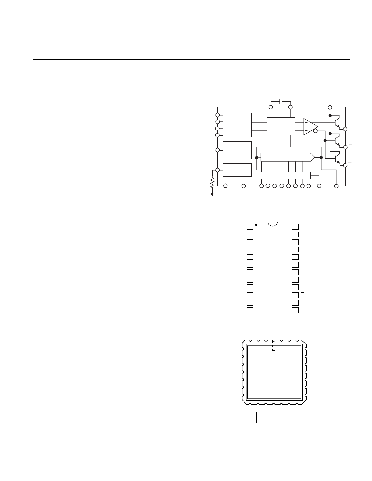
FUNCTIONAL BLOCK DIAGRAM
PIN CONFIGURATIONS
R
NC = NO CONNECT
One Technology Way, P.O. Box 9106, Norwood, MA 02062-9106, U.S.A.
Tel: 781/329-4700 World Wide Web Site: http://www.analog.com
Fax: 781/326-8703 © Analog Devices, Inc., 1999

AD9500–SPECIFICATIONS
ABSOLUTE MAXIMUM RATINGS
1
Positive Supply Voltage (+VS) . . . . . . . . . . . . . . . . . . . . . +7 V
Negative Supply Voltage (–V
) . . . . . . . . . . . . . . . . . . . . –7 V
S
ECL COMMON to Ground Differential . . . . –2.0 V to +5.0 V
Digital Input Voltage Range . . . . . . . . . . . . . –3.5 V to +5.0 V
Trigger/Reset Input Voltage Range . . . . . . . . . . . . . . . ±5.0 V
Trigger/Reset Differential Voltage . . . . . . . . . . . . . . . . . .5.0 V
Minimum R
. . . . . . . . . . . . . . . . . . . . . . . . . . . . . . . 220 Ω
SET
Digital Output Current (
Offset Adjust Current (Sinking) . . . . . . . . . . . . . . . . . . . 4 mA
) . . . . . . . . . . . . . . . . . . . . 2 mA
Q
R
Operating Temperature Range
AD9500BP/BQ . . . . . . . . . . . . . . . . . . . . . –25°C to +85°C
AD9500TE/TQ . . . . . . . . . . . . . . . . . . . . –55°C to +125°C
Storage Temperature Range . . . . . . . . . . . . –65°C to +150°C
Junction Temperature . . . . . . . . . . . . . . . . . . . . . . . . .+175°C
Lead Soldering Temperature (10 sec) . . . . . . . . . . . . .+300°C
Digital Output Current (Q and Q) . . . . . . . . . . . . . . . 30 mA
ELECTRICAL CHARACTERISTICS
2
(Supply Voltages +VS = +5.0 V, VS = –5.2 V; C
= 0 pF; R
EXT
= 500 ⍀ unless otherwise noted)
SET
–25ⴗC to +85ⴗC –55ⴗC to +125ⴗC
Test AD9500BP/BQ AD9500TE/TQ
Parameter Level Temp Min Typ Max Min Typ Max Units
RESOLUTION 8 8 Bits
ACCURACY
3
Differential Linearity I +25°C 0.5 0.5 LSB
Integral Linearity I +25°C 1.0 1.0 LSB
Monotonicity I +25°C Guaranteed Guaranteed
DIGITAL INPUT
Logic “1” Voltage VI Full 2.0 2.0 V
Logic “0” Voltage VI Full 0.8 0.8 V
Logic “1” Current VI Full 5 5 µA
Logic “0” Current VI Full 5 5 µA
Digital Input Capacitance VI +25°C 5.5 5.5 pF
Data Setup Time
Data Hold Time
Latch Pulsewidth (t
RESET/TRIGGER INPUTS
4
5
) V +25°C 3.0 3.0 ns
LPW
6
V +25°C 0.4 0.75 0.4 0.75 ns
V +25°C 0.4 0.75 0.4 0.75 ns
TRIGGER Input Voltage Range IV Full –2.5; 4.5 –2.5; 4.5 V
RESET Input Voltage Range IV Full –2.5; 2.0 –2.5; 2.0 V
Differential Switching Voltage IV Full 40 300 40 300 mV
Input Bias Current I +25°C 4050 4050µA
VI Full 75 75 µA
Input Resistance IV +25°C4 4 kΩ
Input Capacitance IV +25°C 6.5 7.25 6.5 7.25 pF
Minimum Input Pulsewidth
t
, t
TPW
RPW
DYNAMIC PERFORMANCE
Maximum Trigger Rate IV +25°C 60 60 MHz
Minimum Propagation Delay (t
Minimum Propagation Delay TC V Full 7.5 7.5 ps/°C
Full-Scale Range TC
9
Delay Uncertainty (Jitter) V +25°C10 10 ps
Reset Propagation Delay (t
Reset-to-Trigger Holdoff (t
Trigger-to-Reset Holdoff (t
Minimum Output Pulsewidth V +25°C 3.3 3.3 ns
Output Rise Time
Output Fall Time
7
7
Delay Coefficient Settling Time (t
Linear Ramp Settling Time (t
7
8
)
PD
10
)
RD
11
)
THO
12
)
RHO
DAC
) V +25°C22 22 ns
LRS
V +25°C 2.0 2.0 ns
I +25°C 5.4 6.4 7.4 5.4 6.4 7.4 ns
V Full 0.5 0.5 ps/°C
I +25°C 5.4 6.4 7.4 5.4 6.4 7.4 ns
IV +25°C 0.2 0 0.2 0 ns
IV +25°C 2.0 1.5 2.0 1.5 ns
I +25°C 2.0 2.0 ns
I +25°C 2.0 2.0 ns
13
)
V +25°C29 29 ns
REV. D–2–

AD9500
–25ⴗC to +85ⴗC –55ⴗC to +125ⴗC
Test AD9500BP/BQ AD9500TE/TQ
Parameter Level Temp Min Typ Max Min Typ Max Units
SUPPORT FUNCTIONS
ECL
ECL
REF
Voltage Drift
REF
14
Offset Adjust Range V Full –2 –2 mA
DIGITAL OUTPUTS
7
Logic “1” Voltage VI Full –1.1 –1.1 V
Logic “0” Voltage VI Full –1.5 –1.5 V
POWER SUPPLY
15
Positive Supply Current (+5.0 V) I +25°C 2428 2428mA
Negative Supply Current (–5.2 V) I +25°C 3742 3742mA
Nominal Power Dissipation V +25°C 312 312 mW
Power Supply Rejection Ratio
16
Full-Scale Range Sensitivity I +25°C 70 300 70 300 ps/V
Minimum Propagation Delay
Sensitivity I +25°C 150 500 150 500 ps/V
NOTES
1
Absolute maximum ratings are limiting values, to be applied individually, and beyond which serviceability of the circuit may be impaired. Functional operability under
any of these conditions is not necessarily implied. Exposure to absolute maximum rating conditions for extended periods may affect device reliability.
2
Typical thermal impedance
24-Lead Cerdip θ
28-Leadless PLCC (Plastic) θ
28-Leaded Ceramic LCC θ
3
R
= 10 kΩ (Full-scale delay = 100 ns).
SET
4
The digital data inputs must remain stable for the specified time prior to the LATCH ENABLE signal.
5
The digital data inputs must remain stable for the specified time after the LATCH ENABLE signal.
6
The TRIGGER and RESET inputs are differential and must be driven relative to one another. Both of these inputs are ECL compatible, but can also be used with
TTL logic families in a limited fashion.
7
Outputs terminated through 50 Ω resistors to –2.0 V.
8
Program Delay = 0.0 ps (Digital Data = 00H). In Operation, any programmed delays are in addition to the Minimum Propagation Delay.
9
Change in total delay through AD9500, exclusive of changes in minimum propagation delay tPD.
10
Measured from the 50% transition point of the reset signal input, to the 50% transition point of the resetting output.
11
Minimum time from falling edge of RESET to triggering input, to ensure a valid output event.
12
Minimum time from triggering event to rising edge of RESET, to ensure a valid output event.
13
Measured from the LATCH ENABLE input to the point when the AD9500 becomes 8-bit accurate again, after a full-scale change in the programmed delay.
14
Standard 10K and 10KH ECL families operate with a 1.1 mV/°C drift by design.
15
Supply voltages should remain stable within ±5% for normal operation.
16
Measured at ±5% of –V
Specifications subject to change without notice.
and +VS.
S
= 56°C/W; θJC = 16°C/W
JA
= 60°C/W; θJC = 22°C/W
JA
= 69°C/W; θJC = 25°C/W
JA
IV +25°C –1.4 –1.3 –1.2 –1.4 –1.3 –1.2 V
V Full 1.1 1.1 mV/°C
VI Full 30 30 mA
VI Full 44 44 mA
EXPLANATION OF TEST LEVELS
Test Level
I – 100% production tested.
II – 100% production tested at +25°C, and sample tested at
specified temperatures.
III – Periodically sample tested.
IV – Parameter is guaranteed by design and characterization
testing.
V – Parameter is a typical value only.
VI – All devices are 100% production tested at +25°C. 100%
production tested at temperature extremes for extended
temperature devices; sample tested at temperature extremes for commercial/industrial devices.
REV. D
ORDERING GUIDE
Temperature Package Package
Model Ranges Descriptions Options
AD9500BP –25°C to +85°C 28-Leadless PLCC (Plastic),
Industrial Temperature P-28A
AD9500BQ –25°C to +85°C 24-Lead Cerdip,
Industrial Temperature Q-24
AD9500TE –55°C to +125°C 28-Leaded LCC,
Extended Temperature E-28A
AD9500TQ –55°C to +125°C 24-Lead Cerdip,
Extended Temperature Q-24
–3–

AD9500
PIN FUNCTION DESCRIPTIONS
Pin Name Description
D
4–D6
D
(MSB) One of eight digital inputs used to set the programmed delay. D7 (MSB) is the most significant bit of the
7
ECL
REF
OFFSET ADJUST The OFFSET ADJUST is used to adjust the minimum propagation delay (t
C
S
+V
S
TRIGGER Noninverted input of the edge-sensitive differential trigger input stage. The output at Q will be delayed by
TRIGGER Inverted input of the edge-sensitive differential trigger input stage. The output at Q will be delayed by the
RESET Inverted input of the level-sensitive differential reset input stage. The output at Q will be reset after a signal
RESET Noninverted input of the level-sensitive differential reset input stage. The output at Q will be reset after a
Q One of two complementary ECL outputs. A “triggering” event at the inputs will produce a logic HIGH on
Q One of two complementary ECL outputs. A “triggering” event at the inputs will produce a logic LOW on
Q
R
ECL COMMON The collector common for the ECL output stage. The collector common may be tied to +5.0 V, but nor-
–V
S
R
S
GROUND The ground return for the TTL and analog inputs.
LATCH ENABLE Transparent TTL latch control line. A logic HIGH on the LATCH ENABLE freezes the digital code at the
D
(LSB) One of eight digital inputs used to set the programmed delay. D0 (LSB) is the least significant bit of the
0
D3–D
1
One of eight digital inputs used to set the programmed delay.
digital input word.
ECL midpoint reference, nominally –1.3 V. Use of the ECL
allows either of the TRIGGER or RESET
REF
inputs to be configured for single-ended ECL inputs.
), by pulling or pushing a
PD
small current out of or into the pin.
CS allows the full-scale range to be extended by using an external timing capacitor. The value of C
connected between C
See R
S
(C
INTERNAL
= 10 pF).
and +V
S
, may range from no external capacitance to 0.1 µF+.
S
EXT
,
Positive supply terminal, nominally +5.0 V.
the programmed delay, after the triggering event. The programmed delay is set by the digital input word.
The TRIGGER input must be driven in conjunction with the TRIGGER input.
programmed delay, after the triggering event. The programmed delay is set by the digital input word. The
TRIGGER input must be driven in conjunction with the TRIGGER input.
is received at the reset inputs. In the “minimum configuration,” the minimum output pulsewidth will be
equal to the “reset propagation delay,” t
. The RESET input must be driven in conjunction with the
RD
RESET input.
signal is received at the reset inputs. In the “minimum configuration,” the minimum output pulsewidth will
be equal to the “reset propagation delay,” t
. The RESET input must be driven in conjunction with the
RD
RESET input.
the Q output. A “resetting” event at the inputs will produce a logic LOW on the Q output.
the Q output. A “resetting” event at the inputs will produce a logic HIGH on the Q output.
output is parallel to the Q output. The
Q
R
ing output pulsewidths. A “triggering” event at the inputs will produce a logic LOW on the
“resetting” event at the inputs will produce a logic HIGH on the
output is typically used to drive delaying circuits for extend-
Q
R
output.
Q
R
output. A
Q
R
mally it is tied to the circuit ground for standard ECL outputs.
Negative supply terminal, nominally –5.2 V.
RS is the reference current setting terminal. An external setting resistor, R
determines the internal reference current. See C
–V
S
(250 Ω ≤ R
S
≤ 50 kΩ).
SET
, connected between RS and
SET
logic inputs. A logic LOW on the LATCH ENABLE allows the internal current levels to be continuously
updated through the logic inputs D
thru D7.
0
digital input word.
One of eight digital inputs used to set the programmed delay.
–4–
REV. D
 Loading...