

Page 1
Triple 8-Bit, 140 MSPS
a
FEATURES
140 MSPS Guaranteed Conversion Rate
100 MSPS Low Cost Version Available
330 MHz Analog Bandwidth
1 V p-p Analog Input Range
Internal 2.5 V Reference
Differential or Single-Ended Clock Input
3.3 V/5.0 V Three-State CMOS Outputs
Single or Demultiplexed Output Ports
Data Clock Output Provided
Low Power: 1.0 W Typical
5 V Converter Power Supply
APPLICATIONS
RGB Graphics Processing
High Resolution Video
LCD Monitors and Projectors
Micromirror Projectors
Plasma Display Panels
Scan Converters
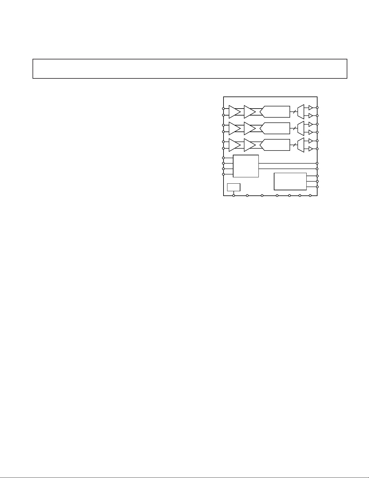
R AIN
R AIN
G AIN
G AIN
B AIN
B AIN
ENCODE
ENCODE
DS
DS
A/D Converter
AD9483
FUNCTIONAL BLOCK DIAGRAM
AD9483
T/H
T/H
T/H
TIMING
2.5V
VREF
RVREFINGVREFINBVREFINV
OUT
QUANTIZER
QUANTIZER
QUANTIZER
8
8
8
CONTROL
CC
GND
V
DD
DRA
7-0
DRB
7-0
DGA
7-0
DGB
7-0
DBA
7-0
B
D
7-0
B
CLKOUT
CLKOUT
OMS
I/P
PD
GENERAL DESCRIPTION
The AD9483 is a triple 8-bit monolithic analog-to-digital
converter optimized for digitizing RGB graphics signals from
personal computers and workstations. Its 140 MSPS encode
rate capability and full-power analog bandwidth of 330 MHz
supports display resolutions of up to 1280 × 1024 at 75 Hz with
sufficient input bandwidth to accurately acquire and digitize
each pixel.
To minimize system cost and power dissipation, the AD9483
includes an internal 2.5 V reference and track-and-hold circuit.
The user provides only a 5 V power supply and an encode clock.
No external reference or driver components are required for
many applications. The digital outputs are three-state CMOS
outputs. Separate output power supply pins support interfacing
with 3.3 V or 5 V logic.
The AD9483’s encode input interfaces directly to TTL, CMOS,
or positive ECL logic and will operate with single-ended or
differential inputs. The user may select dual channel or single
channel digital outputs. The Dual Channel (demultiplexed)
mode interleaves ADC data through two 8-bit channels at onehalf the clock rate. Operation in Dual Channel mode reduces
the speed and cost of external digital interfaces while allowing
the ADCs to be clocked to the full 140 MSPS conversion rate.
In the Single Channel mode, all data is piped at the full clock
rate to the Channel A outputs and the ADCs conversion rate is
limited to 100 MSPS. A data clock output is provided at the
Channel A output data rate for both Dual Channel or Single
Channel output modes.
Fabricated in an advanced BiCMOS process, the AD9483 is
provided in a space-saving 100-lead MQFP surface-mount
plastic package (S-100) and is specified over the 0°C to 85°C
temperature range.
REV. C
Information furnished by Analog Devices is believed to be accurate and
reliable. However, no responsibility is assumed by Analog Devices for its
use, nor for any infringements of patents or other rights of third parties that
may result from its use. No license is granted by implication or otherwise
under any patent or patent rights of Analog Devices. Trademarks and
registered trademarks are the property of their respective owners.
One Technology Way, P.O. Box 9106, Norwood, MA 02062-9106, U.S.A.
Tel: 781/329-4700 www.analog.com
Fax: 781/326-8703 © 2004 Analog Devices, Inc. All rights reserved.
Page 2

(VCC = 5 V, VDD = 3.3 V, external reference, ENCODE = maximum conversion rate
AD9483–SPECIFICATIONS
differential PECL)
Test AD9483KS-140 AD9483KS-100
Parameter Temperature Level Min Typ Max Min Typ Max Unit
RESOLUTION 8 8 Bits
DC ACCURACY
Differential Nonlinearity 25°CI 0.8 1.25/–1.0 0.8 1.25/–1.0 LSB
Full VI 1.50/–1.0 1.50/–1.0 LSB
Integral Nonlinearity 25°CI 0.9 1.50/–1.50 0.9 1.50/–1.50 LSB
Full VI 1.75/–1.75 1.75/–1.75 LSB
No Missing Codes Full VI Guaranteed Guaranteed
Gain Error
Gain Tempco
1
1
25°CI ± 1 ± 2 ± 1 ± 2% FS
Full V 160 160 ppm/°C
ANALOG INPUT
Input Voltage Range
(With Respect to AIN) Full V ± 512 ± 512 mV p–p
Compliance Range AIN or AIN Full V 1.8 3.2 1.8 3.2 V
Input Offset Voltage 25°CI ± 4 ± 16 ± 4 ± 16 mV
Full VI ± 20 ± 20 mV
Input Resistance 25°CI3583 35 83 kΩ
Full VI 25 25 kΩ
Input Capacitance 25°CV 4 4 pF
Input Bias Current 25°CI 1736 17 36 µA
Full VI 50 50 µA
Analog Bandwidth, Full Power 25°CV 330 330 MHz
REFERENCE OUTPUT
Output Voltage Full VI +2.4 +2.5 +2.6 +2.4 +2.5 +2.6 V
Temperature Coefficient Full V 110 110 ppm/°C
SWITCHING PERFORMANCE
Maximum Conversion Rate Full VI 140 100 MSPS
Minimum Conversion Rate Full IV 10 10 MSPS
Encode Pulse Width High (t
Encode Pulse Width Low (t
Aperture Delay (t
)25°CV 1.5 1.5 ns
A
)25°CIV2.8 50 4.0 50 ns
EH
)25°CIV2.8 50 4.0 50 ns
EL
Aperture Delay Matching 25°CV 100 100 ps
Aperture Uncertainty (Jitter) 25°CV 2.3 2.3 ps rms
Data Sync Setup Time (t
Data Sync Hold Time (t
Data Sync Pulsewidth (t
Output Valid Time (t
Output Propagation Delay (t
Clock Valid Time (t
CV
Clock Propagation Delay (t
Data to Clock Skew (t
Data to Clock Skew (tPD–t
)25°CIV0 0 ns
SDS
)25°CIV0.5 0.5 ns
HDS
)25°CIV2.0 2.0 ns
PWDS
2
)
V
PD
3
)
CPD
) Full VI –1.0 0 +1.0 –1.0 0 +1.0 ns
V–tCV
) Full VI –2.0 0 +2.0 –2.0 0 +2.0 ns
CPD
Full VI 4.0 6.3 4.0 6.3 ns
2
)
Full VI 8.0 10 8.0 10 ns
Full VI 3.8 6.2 3.8 6.2 ns
3
)
Full VI 8.0 10 8.0 10 ns
DIGITAL INPUTS
Input Capacitance 25°CV 3 3 pF
DIFFERENTIAL INPUTS
Differential Signal Amplitude (VID) Full IV 400 400 mV
HIGH Input Voltage (V
LOW Input Voltage (V
IHD
ILD
Common-Mode Input (V
HIGH Level Current (I
IH
) Full IV 0.4 V
CC
) Full IV 0 0 V
) Full IV 1.5 1.5 V
ICM
) Full VI 1.2 1.2 mA
0.4 V
CC
V
LOW Level Current (IIL) Full VI 1.2 1.2 mA
VREF IN
Input Resistance 25°CV 2.5 2.5 kΩ
–2–
REV. C
Page 3

AD9483
Test AD9483KS-140 AD9483KS-100
Parameter Temperature Level Min Typ Max Min Typ Max Unit
SINGLE-ENDED INPUTS
HIGH Input Voltage (VIH) Full IV 2.0 V
LOW Input Voltage (V
HIGH Level Current (I
) Full IV 0 0.8 0 0.8 V
IL
) Full VI 1 1 mA
IH
CC
LOW Level Current (IIL) Full VI 1 1 mA
DIGITAL OUTPUTS
Logic “1” Voltage Full VI V
– 0.05 V
DD
Logic “0” Voltage Full VI 0.05 0.05 V
Output Coding Binary Binary
POWER SUPPLY
V
Supply Current Full VI 215 215 mA
CC
V
Supply Current Full VI 60 60 mA
DD
Total Power Dissipation
4
Full VI 1.0 1.3 1.0 1.3 W
Power-Down Supply Current 25°CV 420 420mA
Power-Down Dissipation 25°CV 20100 20 100 mW
DYNAMIC PERFORMANCE
5
Transient Response 25°CV 1.5 1.5 ns
Overvoltage Recovery Time 25°CV 1.5 1.5 ns
Signal-to-Noise Ratio (SNR)
(Without Harmonics)
= 19.7 MHz 25°CV 45 45 dB
f
IN
= 49.7 MHz 25°CI4144 41 44 dB
f
IN
= 69.7 MHz 25°CV 44 44 dB
f
IN
Signal-to-Noise Ratio (SINAD)
(With Harmonics)
= 19.7 MHz 25°CV 44 44 dB
f
IN
f
= 49.7 MHz 25°CI4043 40 43 dB
IN
= 69.7 MHz 25°CV 42 42 dB
f
IN
Effective Number of Bits
= 19.7 MHz 25°CV 7.0 7.0 Bits
f
IN
= 49.7 MHz 25°CI6.4 6.8 6.4 6.8 Bits
f
IN
= 69.7 MHz 25°CV 6.8 6.8 Bits
f
IN
2nd Harmonic Distortion
= 19.7 MHz 25°CV 63 63 dBc
f
IN
= 49.7 MHz 25°CI5058 50 58 dBc
f
IN
f
= 69.7 MHz 25°CV 51 51 dBc
IN
3rd Harmonic Distortion
= 19.7 MHz 25°CV 56 56 dBc
f
IN
f
= 49.7 MHz 25°CI4654 46 54 dBc
IN
= 69.7 MHz 25°CV 51 51 dBc
f
IN
Crosstalk Full V 55 55 dB
NOTES
1
Gain error and gain temperature coefficient are based on the ADC only (with a fixed 2.5 V external reference).
2
tV and t
3
tCV and t
4
Measured under the following conditions: analog input is –1 dBFS at 19.7 MHz.
5
SNR/harmonics based on an analog input voltage of –1.0 dBFS referenced to a 1.024 V full-scale input range.
Typical thermal impedance for the S-100 (MQFP) 100-lead package: θJC = 10°C/W, θCA = 17°C/W, θJA = 27°C/W.
Specifications subject to change without notice.
are measured from the threshold crossing of the ENCODE input to valid TTL levels at the digital outputs. The output ac load during test is 5 pF.
PDF
are measured from the threshold crossing of the ENCODE input to valid TTL levels at the digital outputs. The output ac load during test is 20 pF.
CPD
2.0 V
– 0.05 V
DD
CC
V
REV. C
–3–
Page 4
AD9483
ABSOLUTE MAXIMUM RATINGS*
VCC . . . . . . . . . . . . . . . . . . . . . . . . . . . . . . . . . . . . . . . . . . 6 V
. . . . . . . . . . . . . . . . . . . . . . . . . . . . . . . . . . . . . . . . . . 6 V
V
DD
Analog Inputs . . . . . . . . . . . . . . . . . . . . . . . . . . . V
VREF IN, VREF OUT . . . . . . . . . . . . . . . . . . . . V
Digital Inputs . . . . . . . . . . . . . . . . . . . . . . . . . . . V
to 0.0 V
CC
to 0.0 V
CC
to 0.0 V
CC
Digital Output Current . . . . . . . . . . . . . . . . . . . . . . . . 20 mA
Operating Temperature . . . . . . . . . . . . . . . . . . . . 0°C to 85°C
Storage Temperature . . . . . . . . . . . . . . . . . . –65°C to +150°C
Maximum Junction Temperature . . . . . . . . . . . . . . . . . 150°C
Maximum Case Temperature . . . . . . . . . . . . . . . . . . . . 150°C
*Stresses above those listed under Absolute Maximum Ratings may cause perma-
nent damage to the device. This is a stress rating only; functional operation of the
device at these or any other conditions above those indicated in the operational
sections of this specification is not implied. Exposure to absolute maximum ratings
for extended periods may effect device reliability.
EXPLANATION OF TEST LEVELS
Test Level
I–100% production tested.
II – 100% production tested at 25°C and sample tested at
specified temperatures.
III – Periodically sample tested.
IV – Parameter is guaranteed by design and characterization
testing.
V–Parameter is a typical value only.
VI – 100% production tested at 25°C; guaranteed by design
and characterization testing.
Table I. Output Coding
Step AIN–AIN Code Binary
255 ≥0.512 V 255 1111 1111
254 0.508 V 254 1111 1110
253 0.504 V 253 1111 1101
•• • •
•• • •
•• • •
129 0.006 V 129 1000 0001
128 0.002 V 128 1000 0000
127 –0.002 V 127 0111 1111
126 –0.006 V 126 0111 1110
•• • •
•• • •
•• • •
2 –0.504 V 2 0000 0010
1 –0.508 V 1 0000 0001
0 ≤–0.512 V 0 0000 0000
ORDERING GUIDE
Temperature Package Package
Model Range Description Option
AD9483KS-100 0°C to 85°CMetric Quad Flat Package S-100B
AD9483KS-140 0°C to 85°CMetric Quad Flat Package S-100B
AD9483/PCB Evaluation Board
CAUTION
ESD (electrostatic discharge) sensitive device. Electrostatic charges as high as 4000 V readily
accumulate on the human body and test equipment and can discharge without detection.
Although the AD9483 features proprietary ESD protection circuitry, permanent damage may
occur on devices subjected to high-energy electrostatic discharges. Therefore, proper ESD
precautions are recommended to avoid performance degradation or loss of functionality.
WARNING!
ESD SENSITIVE DEVICE
–4–
REV. C
Page 5

AD9483
PIN FUNCTION DESCRIPTIONS
Pin Number Mnemonic Function
1, 6, 7, 10, 20, 30, 40, 50,
60, 70, 73, 77, 78, 80, 81,
95, 96, 100 GND Ground
2 ENCODE Encode Clock for ADC (ADC Samples on Rising Edge of ENCODE)
3 ENCODE Encode Clock Complement (ADC Samples on Falling Edge of ENCODE)
4DSData Sync Aligns Output Channels in Dual-Channel Mode
5 DS Data Sync Complement
8 DCO Data Clock Output. Clock Output at Channel A Data Rate
9 DCO Data Clock Output Complement
11, 21, 31, 41, 51, 61, 71 V
79, 82, 83, 93, 94, 98, 99 V
12–19 D
22–29 D
32–39 D
42–49 D
52–59 D
62–69 D
DD
CC
BB7–DBB0
BA7–DBA0
GB7–DGB0
GA7–DGA0
RB7–DRB0
RA7–DRA0
72 NC No Connect
74 OMS Selects Single Channel or Dual Channel Output Mode, (HIGH = Single,
75 I/P Selects Interleaved or Parallel Output Mode, (HIGH = Interleaved, LOW = Parallel)
76 PD Power-Down and Three-State Select (HIGH = Power-Down)
84 R AIN Analog Input Complement for Converter “R”
85 R AIN Analog Input True for Converter “R”
86 R REF IN Reference Input for Converter “R” (2.5 V Typical, ±10%)
87 G AIN Analog Input Complement for Converter “G”
88 G AIN Analog Input True for Converter “G”
89 G REF IN Reference Input for Converter “G” (2.5 V Typical, ±10%)
90 B AIN Analog Input Complement for Converter “B”
91 B AIN Analog Input True for Converter “B”
92 B REF IN Reference Input for Converter “B” (2.5 V Typical, ± 10%)
97 REF OUT Internal Reference Output (2.5 V Typical); Bypass with 0.01 µF to Ground
Output Power Supply. Nominally 3.3 V
Converter Power Supply. Nominally 5.0 V
Digital Outputs of Converter “B,” Channel B. DBB7 is the MSB
Digital Outputs of Converter “B,” Channel A. DBA7 is the MSB
Digital Outputs of Converter “G,” Channel B. DGB7 is the MSB
Digital Outputs of Converter “G,” Channel A. DGA7 is the MSB
Digital Outputs of Converter “R,” Channel B. DRB7 is the MSB
Digital Outputs of Converter “R,” Channel A. DRA7 is the MSB
LOW = Demuxed)
REV. C
–5–
Page 6
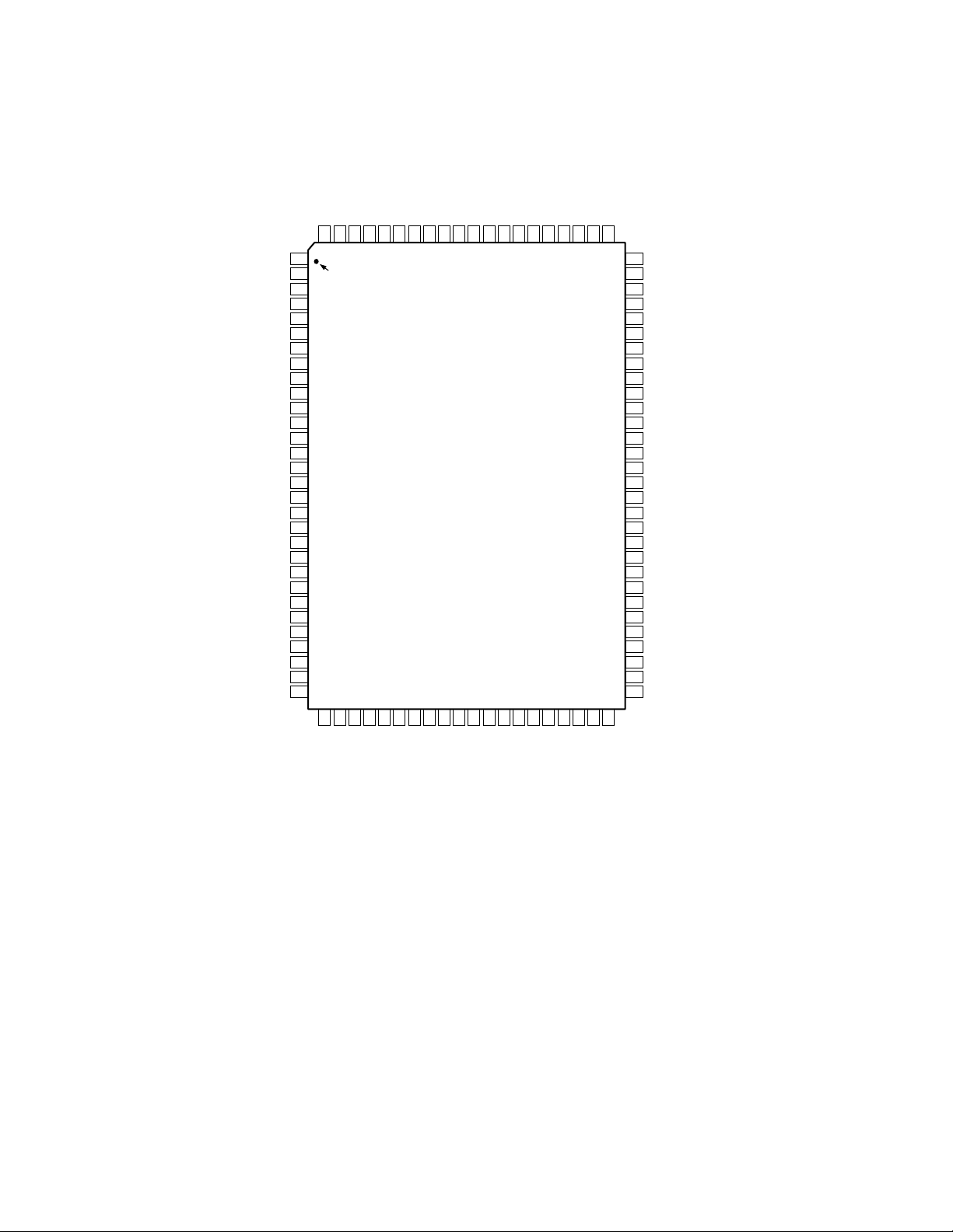
AD9483
GND
1
GND
GND
DCO
DCO
GND
V
DBB
DBB
DBB
DBB
DBB
DBB
DBB
DBB
GND
V
DBA
DBA
DBA
DBA
DBA
DBA
DBA
DBA
GND
DS
DS
2
3
4
5
6
7
8
9
10
11
DD
12
7
13
6
14
5
15
4
16
3
17
2
18
1
19
0
20
21
DD
22
7
23
6
24
5
25
4
26
3
27
2
28
1
29
0
30
ENCODE
ENCODE
NC = NO CONNECT
PIN CONFIGURATION
Metric Quad Flat Package (S-100B)
CC
CC
V
V
GND
100
PIN 1
IDENTIFIER
GND
REF OUT
99989796959493
GND
CC
CC
B AIN
V
V
B REF IN
929190
B AIN
G REF IN
G AIN
89
88
G AIN
8786858483
AD9483
TOP VIEW
(PINS DOWN)
31
33
32
7
6
B
B
DD
G
G
V
D
D
37
35
34
5
4
B
B
G
G
D
D
39
40
38
36
3
2
B
B
G
G
D
D
41
43
44
1
B
G
D
42
0
B
G
GND
D
5
7
6
A
A
A
DD
G
G
G
V
D
D
D
R AIN
R REF IN
46
45
4
3
A
A
G
G
D
D
R AIN
47
2
A
G
D
CC
CC
GND
V
V
81
82
80
GND
79
V
CC
78
GND
77
GND
76
PD
75
I/P
74
OMS
73
GND
72
NC
71
V
DD
70
GND
69
DRA
0
68
DRA
1
67
DRA
2
66
DRA
3
65
DRA
4
64
DRA
5
63
DRA
6
62
DRA
7
61
V
DD
60
GND
59
DRB
0
58
DRB
1
57
DRB
2
56
DRB
3
55
DRB
4
54
DRB
5
DRB
53
6
52
DRB
7
51
V
DD
50
49
48
1
0
A
A
G
G
GND
D
D
–6–
REV. C
Page 7
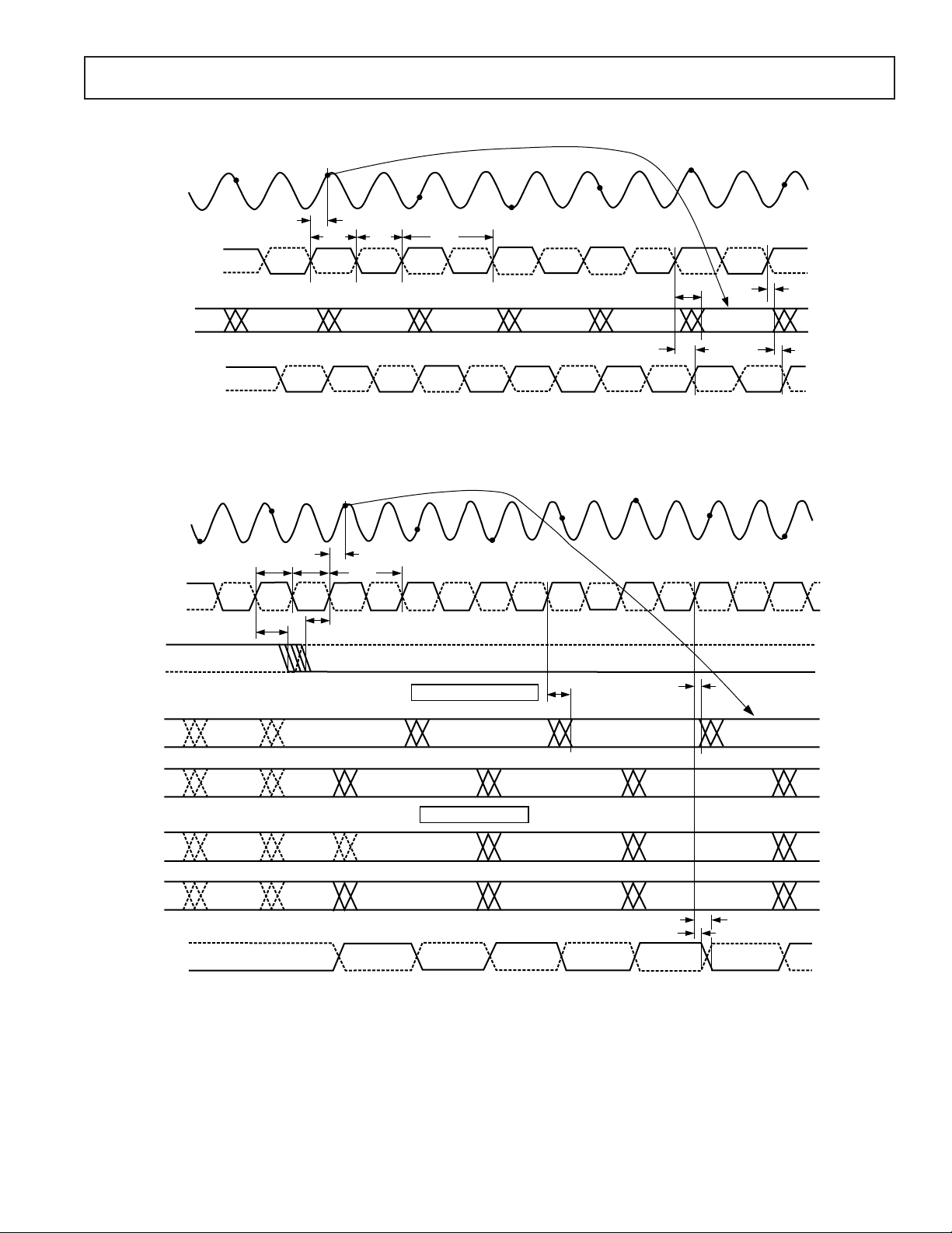
TIMING
AD9483
AIN
ENCODE
ENCODE
DS
AIN
ENCODE
ENCODE
D7–D 0
CLOCK OUT
CLOCK OUT
SAMPLE N–2
SAMPLE N–1
SAMPLE N
t
EH
SAMPLE N+3
A
SAMPLE N+1
t
EL
1/f
t
SAMPLE N+2
S
SAMPLE N+4
t
DATA N–5 DATA N–4 DATA N–3 DATA N–2 DATA N–1 DATA N
t
CPD
Figure 1. Timing—Single Channel Mode
SAMPLE N–1
t
EH
t
HDS
t
EL
t
SDS
SAMPLE N
t
A
1/f
SAMPLE N+1
S
SAMPLE N+2
SAMPLE N+3
SAMPLE N+4
SAMPLE N+5
PD
t
V
t
CV
SAMPLE N+6
DS
PORT A
D7–D0
PORT B
D7–D0
PORT A
D7–D0
PORT B
D7–D0
CLKOUT
CLKOUT
DATA N–7
OR N–8
DATA N–8
OR N–7
DATA N–9
OR N–8
DATA N–8
OR N–7
DATA N–7
DATA N–6
OR N–7
DATA N–7
OR N–8
DATA N–6
OR N–7
INTERLEAVED DATA OUT
OR N–6
INVALID IF OUT OF SYNC
DATA N–5 IF IN SYNC
INVALID IF OUT OF SYNC
DATA N–5 IF IN SYNC
INVALID IF OUT OF SYNC
DATA N–4 IF IN SYNC
PARALLEL DATA OUT
DATA N–7
OR N–6
DATA N–3
INVALID IF OUT OF SYNC
DATA N–4 IF IN SYNC
DATA N–3
Figure 2. Timing—Dual Channel Mode
t
PD
DATA N–2
t
V
DATA N
DATA N–1
DATA N–2
DATA N–1
t
t
CV
CPD
DATA N+1
DATA N
DATA N+1
REV. C
–7–
Page 8
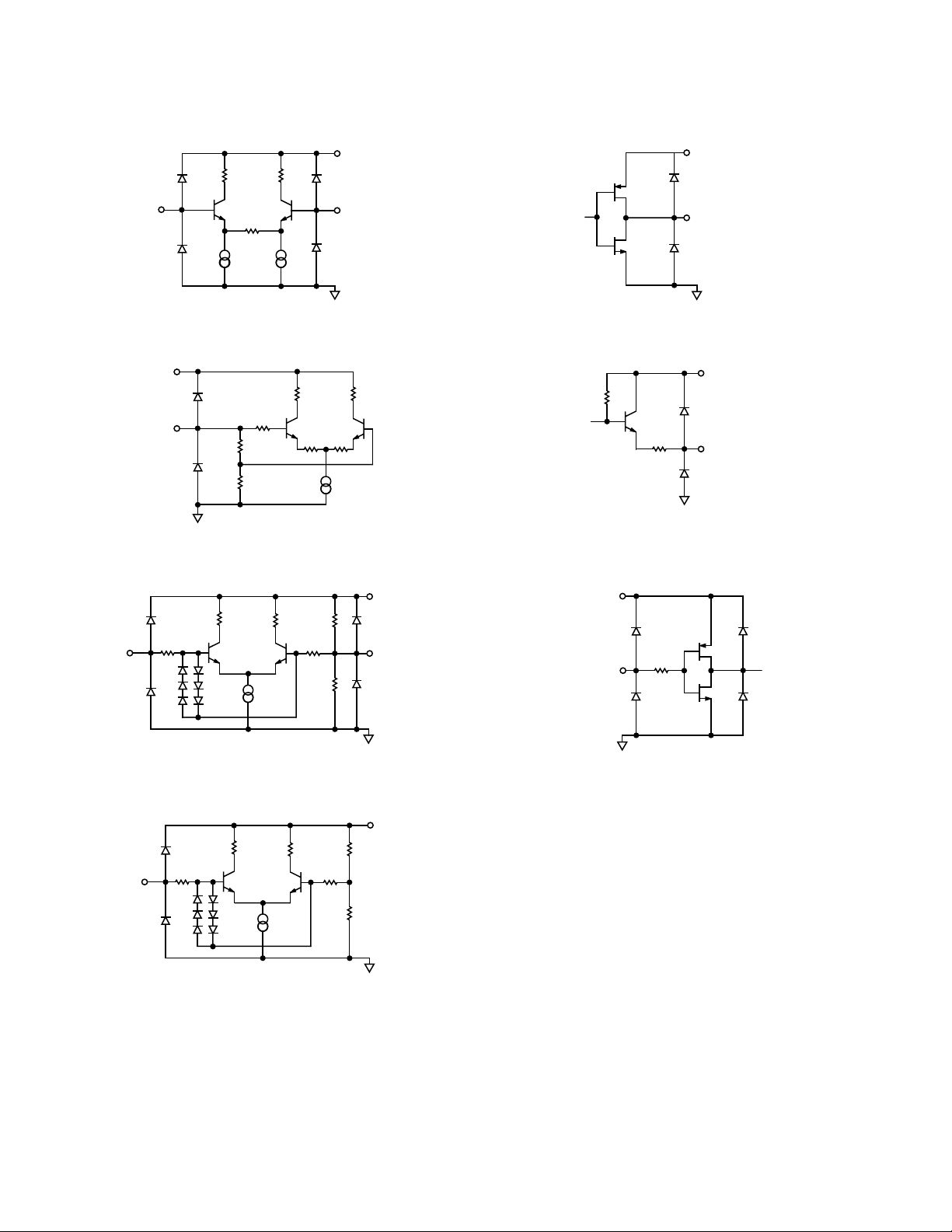
AD9483
V
CC
AD9483
DIGITAL
INPUTS
EQUIVALENT CIRCUITS
V
AIN
AIN
AD9483
Figure 3. Equivalent Analog Input Circuit
V
CC
VREF IN
500⍀
2k⍀
AD9483
Figure 4. Equivalent Reference Input Circuit
17.5k⍀
ENCODE
DS
300⍀
AD9483
300⍀
7.5k⍀
CC
V
CC
ENCODE
DS
V
DD
AD9483
DIGITAL
OUTPUTS
Figure 7. Equivalent Digital Output Circuit
V
CC
VREF
OUT
AD9483
Figure 8. Equivalent Reference Output Circuit
Figure 5. Equivalent Encode and Data Select Input Circuit
V
DEMUX
Figure 6. Equivalent
AD9483
DEMUX
Input Circuit
Figure 9. Equivalent Digital Input Circuit
CC
–8–
REV. C
Page 9
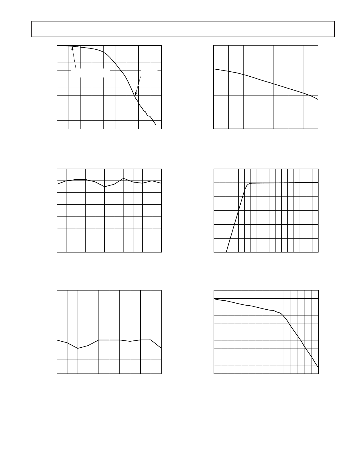
0
TEMPERATURE – ⴗC
–40 0
2.5
–20 20 40 60 80 100
2.48
2.46
2.44
2.42
2.4
VOLTS
1412 130
2.6
2.5
2.4
12345678910
VOLTS
2.3
2.2
2.1
2
1.9
1.8
1.7
1.6
11 15
I
REF
– mA
–0.5
–1
–1.5
–2
–2.5
dB
–3
–3.5
–4
–4.5
–5
050
NYQUIST FREQUENCY
(70MHz)
150 250 300 400 450
100 200 350
f
IN
– MHz
–3dB
(333MHz)
Typical Performance Characteristics–
AD9483
TPC 1. Frequency Response: fS = 140 MSPS
–70
–60
–50
–40
dB
–30
–20
–10
0
05
10 50 100 200 2502.5 7.5 25 75 150
fIN – MHz
TPC 2. Crosstalk vs. fIN: fS = 140 MSPS
–80
–75
TPC 4. Reference Voltage vs. Temperature
2.6
2.5
2.4
2.3
REF
V
2.2
2.1
2
3
3.2 3.4 3.6 3.8 4 4.2
4.4 4.6 4.8 5 5.2 5.4 5.6 5.8 6 6.2 6.4
VCC – V
TPC 5. Reference Voltage vs. Power Supply Voltage
–70
–65
dB
–60
REV. C
–55
–50
0
TPC 3. Crosstalk vs. Temperature: fIN = 70 MHz
10 20 30 40 50 60 70 80 90
TEMPERATURE – ⴗC
100
TPC 6. Reference Voltage vs. Reference Load
–9–
Page 10

AD9483
9
8.5
8
7.5
7
6.5
ns
6
5.5
5
4.5
4
5101520
T
3.3V
PD
TV 5V
LOAD CAPACITANCE – pF
T
5V
PD
TV 3.3V
25 30
TPC 7. Clock Output Delay vs. Capacitance
9
8
VDD – V
T
PD
T
DD
7
6
5
ns
4
3
2
1
0
3 3.3
3.6 3.9 4.2 4.5 4.75 5 5.25 5.5
TPC 8. Output Delay vs. V
5
4.5
4
3.5
3
2.5
VOLTS
2
1.5
1
0.5
0
V
= +3.3V
DD
02 10 16 20
468 1214 18
IOH – mA
V
= +5V
DD
TPC 10. Output Voltage HIGH vs. Output Current
2
1.8
1.6
1.4
V
1.2
1
VOLTS
0.8
0.6
0.4
0.2
0
051015 20
V
DD
= +3.3V
V
= +5V
DD
I
OL
TPC 11. Output Voltage LOW vs. Output Current
9
T
8.5
8
7.5
7
6.5
ns
6
5.5
5
4.5
4
–40 0 50 100
PD
3.3V
T
5V
PD
TEMPERATURE – ⴗC
TV 5V
TV 3.3V
TPC 9. Output Delay vs. Temperature
–10–
600
500
400
300
mW
200
100
0
3 3.5 4 4.5 5 5.5
TPC 12. Output Power vs. VDD, C
VDD – V
LOAD
= 10 pF
REV. C
Page 11

50
SNR
SINAD
f
S
– MSPS
0
dB
30
20 140 180
34
38
42
46
50
32
36
40
44
48
40 60 80 100 120 160 200
MHz
0
dB
–90
10 20 30 40 50 60 70 80 90 100
–80
–70
–60
–50
–40
–30
–20
–10
0
FUNDAMENTAL = –0.5dBFS
SNR = 44.6dB
SINAD = 37.6dB
2ND HARMONIC = 63.1dB
3RD HARMONIC = 39.1dB
48
46
44
42
40
dB
38
36
34
32
30
0
30 60 140 180
100
fS – MSPS
TPC 13. SNR vs. fS: fIN = 19.7 MHz
AD9483
SNR
SINAD
TPC 16. SNR vs fS: fIN = 71.7 MHz
–75
–70
–65
dB
–60
2ND HARMONIC
–55
–50
0
25 50 130 170
TPC 14. Harmonic Distortion vs. fS: fIN = 19.7 MHz
0
–10
–20
–30
–40
dB
–50
–60
–70
REV. C
–80
–90
0
10 20 30 40 50 60 70 80 90 100
TPC 15. Spectrum: fS = 140 MSPS, fIN = 19.57 MHz
3RD HARMONIC
90
f
– MSPS
S
FUNDAMENTAL = –0.5dBFS
SNR = 45.8dB
SINAD = 45.2dB
2ND HARMONIC = 69.8dB
3RD HARMONIC = 61.6dB
MHz
–11–
–56
–54
–52
–50
–48
–46
dB
–44
–42
–40
–38
–36
0
40 80 155 175120
3RD HARMONIC
fS – MSPS
2ND HARMONIC
TPC 17. Harmonic Distortion vs fS: fIN = 71.7 MHz
TPC 18. Spectrum: fS = 140 MSPS, fIN = 70.3 MHz
Page 12

AD9483
46
44
42
40
38
dB
36
34
32
30
fS = 140MSPS
f
= 19.3MHz
IN
28%231%
25%
1.8
38%
2.2
ENCODE DUTY CYCLE – %
ENCODE PULSEWIDTH – ns
2.7
45%
3.2
SNR
52%
3.7
59%
4.2
TPC 19. SNR vs. Clock Pulse Width (t
55
50
45
dB
40
NYQUIST FREQUENCY
(70.0MHz)
SINAD
66%
73%
SNR
5.2
76%
4.7
): fS = 140 MSPS
PWH
5.4
46
SNR
45
44
43
dB
42
41
40
–25
0406080100
SINAD
TEMPERATURE – ⴗC
TPC 22. SNR vs. Temperature, fS = 140 MSPS
–70
–65
–60
–55
dB
–50
35
30
050
100 150 200 250
fIN – MHz
SINAD
TPC 20. SNR vs. fIN: fS = 140 MSPS
–60
–56
–52
dB
–48
–44
–40
–25
0406080100
TEMPERATURE – ⴗC
TPC 21. 3rd Harmonic vs. Temperature, fS = 140 MSPS
–45
–40
–25
0406080100
TEMPERATURE – ⴗC
TPC 23. 2nd Harmonic vs. Temperature, fS = 140 MSPS
0
–10
–20
–30
–40
–50
dB
–60
–70
–80
–90
–100
0
10 20 30 40 50 60 70 80 90 100
MHz
F1 = 55.0MHz
F2 = 56.0MHz
F1 = F2 = –7.0dBFS
TPC 24. Two Tone Intermodulation Distortion
–12–
REV. C
Page 13

AD9483
APPLICATION NOTES
Theory of Operation
The AD9483 combines Analog Devices’ patented MagAmp bitper-stage architecture with flash converter technology to create a
high performance, low power ADC. For ease of use the part
includes an on board reference and input logic that accepts TTL,
CMOS, or PECL levels.
Each of the three analog input signals is buffered by a high speed
differential amplifier and applied to a track-and-hold (T/H)
circuit. This T/H captures the value of the input at the sampling
instant and maintains it for the duration of the conversion. The
sampling and conversion process is initiated by a rising edge on
the ENCODE input. Once the signal is captured by the T/H,
the four Most Significant Bits (MSBs) are sequentially encoded
by the MagAmp string. The residue signal is then encoded by a
flash comparator string to generate the four Least Significant
Bits (LSBs). The comparator outputs are decoded and combined into the 8-bit result.
If the user has selected Single Channel mode (OMS = HIGH)
the 8-bit data word is directed to an A output bank. Data are
strobed to the output on the rising edge of the ENCODE input
with four pipeline delays. If the user has selected Dual Channel
mode (OMS = LOW) the data are alternately directed between
the A and B output banks and the data has five pipeline delays.
At power-up, the N sample data can appear at either the A or B
Port. To align the data in a known state, the user must strobe
DATA SYNC (DS, DS) per the conditions described in the
Timing section.
Graphics Applications
The high bandwidth and low power of the AD9483 makes it very
attractive for applications that require the digitization of presampled waveforms, wherein the input signal rapidly slews from
one level to another, then is relatively stable for a period of time.
Examples of these include digitizing the output of computer
graphic display systems, and very high speed solid state imagers.
These applications require the converter to process inputs with
frequency components well in excess of the sampling rate (often
with subnanosecond rise times), after which the A/D must settle
and sample the input in well under one pixel time. The architecture of the AD9483 is vastly superior to older flash architectures,
which not only exhibit excessive input capacitance (which is very
hard to drive), but can make major errors when fed a very rapidly slewing signal. The AD9483’s extremely wide bandwidth
Track/Hold circuit processes these signals without difficulty.
Using the AD9483
Good high speed design practices must be followed when using the
AD9483. Decoupling capacitors should be physically as close as
possible to the chip to obtain maximum benefit. We recommend
placing a 0.1 µF capacitor at each power ground pin pair (14 total)
for high frequency decoupling and including one 10 µF capacitor for
local low frequency decoupling. Each of the three VREF IN pins
should also be decoupled by a 0.1 µF capacitor.
The part should be located on a solid ground plane and output trace
lengths should be short (<1 inch) to minimize transmission line effects.
This will avoid the need for termination resistors on the output bus
and reduces the load capacitance that needs to be driven, which in
turn minimizes on-chip noise due to heavy current flow in the
outputs. We have obtained optimum performance on our evaluation
board by tying all V
pins to a quiet analog power supply system
CC
and tying all GND pins to a quiet analog system ground.
Minimum Encode Rate
The minimum sampling rate for the AD9483 is 10 MHz for the
140 MSPS and 100 MSPS versions. To achieve this sampling
rate, the Track/Hold circuit employs a very small hold capacitor.
When operated below the minimum guaranteed sampling rate,
the T/H droop becomes excessive. This is first observed as an
increase in offset voltage, followed by degraded linearity at even
lower frequencies.
Lower effective sampling rates may be easily supported by operating the converter in Dual Port output mode and using only
one output channel. A majority of the power dissipated by the
AD9483 is static (not related to conversion rate), so the penalty
for clocking at twice the desired rate is not high.
Digital Inputs
SNR performance is directly related to the sampling clock stability in A/D converters, particularly for high input frequencies
and wide bandwidths.
ENCODE and Data Select (DS) can be driven differentially or
single-ended. For single-ended operation, the complement
inputs (ENCODE, DS) are internally biased to V
/3 (~1.5 V)
DD
by a high impedance on-chip resistor divider (Figure 5), but
they may be externally driven to establish an alternate threshold
if desired. A 0.1 µF decoupling capacitor to ground is sufficient
to maintain a threshold appropriate for TTL or CMOS logic.
When driven differentially, ENCODE and DS will accommodate differential signals centered between 1.5 V and 4.5 V with a
total differential swing ≥800 mV (V
≥400 mV).
ID
Note the 6-diode clock input protection circuitry in Figure 5.
This limits the differential input voltage to ±2.1 V. When the
diodes turn on, current is limited by the 300 Ω series resistor.
Exceeding 2.1 V across the differential inputs will have no
impact on the performance of the converter, but be aware of the
clock signal distortion that may be produced by the nonlinear
impedance at the converter.
DRIVING DIFFERENTIAL INPUTS DIFFERENTIALLY
CLOCK
CLOCK
CLOCK
0.1F
ENC
ENC
ENC
ENC
V
IH D
V
IC M
V
IL D
DRIVING DIFFERENTIAL INPUTS SINGLE-ENDEDLY
V
IN D
V
IC M
V
IL D
V
V
ID
ID
Figure 10. Input Signal Level Definitions
ADC Gain Control
Each of the three ADC channels has independent limited gain
control. The full-scale signal amplitude for a given ADC is set by
the dc voltage on its VREF In pin. The equation relating the full
scale amplitude to VREF In is as follows: FS = (0.4) × (VREF
IN). The three ADCs are optimized for a full-scale signal amplitude of 1 V, but will accommodate up to ±10% variation.
REV. C
–13–
Page 14

AD9483
ADC Offset Control
The offset for each of the three ADCs can be independently
controlled. For a single-ended analog input where the analog
input is connected to a reference, offset can be adjusted simply
by adjusting the dc voltage of the reference. For differential
analog inputs, the user must provide the offset in their signal.
Offset can be adjusted up or down as far as the common-mode
input range will allow.
Power Dissipation
Power dissipation for the AD9483 has two components, V
CC
and VDD. Power dissipation from VCC is relatively constant for a
given supply voltage, whereas power dissipation from VDD can
vary greatly. V
supplies power to the analog circuity. V
CC
DD
supplies power to the digital outputs and can be approximated
by the following equation:
P (V
) = 1/2 C × V2 × F × N
DD
C =Output Load Capacitance
V =V
Supply Voltage
DD
F =Encode Frequency
N =Number of Outputs Switching
Nominally, C = 10 pF, V = 3.3 V, F = 140 MSPS, and N = 26.
N comes from the 24 output bits plus two clock outputs,
P(V
) = 197 mW.
DD
Power-Down
The power-down function allows users to reduce power dissipation when output data is not required. A TTL/CMOS HIGH
signal on pin 76, (PD), shuts down most of the chip and brings
the total power dissipation to less than 100 mW. The internal
bandgap voltage reference remains active during power-down
mode to minimize reactivation time. If the power-down function
is not desired, the PD pin should be tied to ground or held to a
TTL/CMOS LOW level.
Bandgap Voltage Reference
The AD9483 internal reference, VREF OUT (Pin 97), provides
a simple, cost effective reference for many applications. It exhibits reasonable accuracy and excellent stability over power supply
and temperature variations. The reference output can be used to
set the three ADCs’ gain and offset. The reference is capable of
providing up to 1 mA of additional current beyond the requirements of the AD9483.
As the ADC gain and offset are set by the reference inputs,
some applications may require a reference with greater accuracy
or temperature performance. In these cases, an external reference may be connected directly to the VREF IN pins. VREF
OUT, if unused, should be left floating. Note, each of the three
VREF IN pins will require up to 1 mA of current.
Modes of Operation
The AD9483 has three modes of operation, Single Channel
output mode, and a Dual Channel output mode with two possible data formats, interleaved or parallel. Two pins control which
mode of operation the chip is in, Pin 74 Output Mode Select
(OMS) and Pin 75 Interleaved/Parallel Select (I/P). Table II
shows the configuration required for each mode.
Table II. Output Mode Selection
MODE OMS I/P
Dual Channel—Parallel LOW LOW
Dual Channel—Interleaved LOW HIGH
Single Channel HIGH DON’T CARE
Demuxed Output Mode
In demuxed mode, (Pin 74 OMS = LOW), the ADC output
data are alternated between the two output ports (Port A and
Port B). This limits the data output rate to 1/2 the rate of
ENCODE, and facilitates conversion rates up to 140 MSPS.
Demuxed output mode is recommended for guaranteed operation above 100 MSPS, but may be enabled at any specified
conversion rate.
Two data formats are possible in Dual Channel output mode,
parallel data out and interleaved data out. Pin 75 I/P should be
LOW for parallel format and HIGH for interleaved format.
Figures 1 and 2 show the timing requirements for each format.
Note that the Data Sync input, (DS), is required in Dual Channel output mode for both formats. The section on Data Sync
describes the requirements of the Data Sync input.
As shown in Figures 1 and 2, when using the interleaved data
format, a sample is taken on an ENCODE rising edge N. The
resulting data is produced on an output port following the fifth
rising edge of ENCODE after the sample was taken, (five pipeline delays). The following sample, (N+1), will be produced on
the opposite port, also five pipeline delays after it was taken.
The state of CLKOUT when the sample was taken will determine out of which port the data will come. If CLKOUT was
LOW, the data will come out Port A. If CLKOUT was HIGH,
the data will come out Port B.
In order to achieve parallel data format on the two output data
ports, the data is internally aligned. This is accomplished by adding
an extra pipeline delay to just the A Data Port. Thus, data coming out Port A will have six pipeline delays and data coming out
Port B will have five pipeline delays. As with the interleaved
format, the state of Data Sync when a sample is taken will
determine out of which port the data will come. If CLKOUT
was LOW, the data will come out Port A. If CLKOUT was
HIGH, the data will come out Port B.
–14–
REV. C
Page 15

AD9483
Data Sync
The Data Sync input, DS, is required to be driven for most
applications to guarantee at which output port a given sample
will appear. When DS is held high, the ADC data outputs and clock
outputs do not switch—they are held static. Synchronization is
accomplished by the assertion (falling edge) of DS, within the
timing constraints T
SDS
and T
edge. (On initial synchronization T
falls T
before a given encode rising edge N, the analog value
SDS
relative to an encode rising
HDS
is not relevant.) If DS
HDS
at that point in time will be digitized and available at Port A five
cycles later (interleaved mode). The very next sample, N+1, will
be sampled by the next rising encode edge and available at Port
B five cycles after that encode edge (interleaved mode). In dual
parallel mode the A port has a six cycle latency, the B port has a
five cycle latency as described in Demuxed Outputs Mode section.
DS can be asserted once per video line if desired by using the
horizontal sync signal (HSYNC). The start of HSYNC should
occur after the end of active video by at least the chip latency.
The HSYNC front porch is usually much greater than this in a
typical SXGA system. If this is true in a given system then DS
can be reset high by the HSYNC leading edge (the samples at
that point should not be required in a typical system). DS can
then be reasserted (brought low), by triggering from HSYNC
trailing edge—observing T
of the next rising encode edge.
SDS
The first pixel data (on A Port) would be available five cycles
after the first rising encode after HSYNC goes high.
It is possible to use the phase of the data clock outputs and
software programming to accommodate situations where DS is
not driven. The data clock outputs (CLKOUT and CLKOUT)
can be used to determine when data is valid on the output ports.
In these cases DS should be grounded and DS left floating or
connected to V
. If CLKOUT was low when a given sample
CC
was taken, the digitized value will be available on Port A, five
cycles later. Data Sync has no effect when Single Channel
Mode is selected, it should be grounded
Figure 2 shows how to use DS properly. The DS rising edge
does not have any special timing requirements except that no
data will come out of either port while it is held HIGH. The
falling edge of DS must, however, meet a minimum setup-andhold time with respect to the rising edge of ENCODE.
Single Channel Outputs Mode
In Single Channel mode, (Pin 74 OMS = HIGH), the timing
of the AD9483 is similar to any high speed ADC (Figure 1). A
sample is taken on every rising edge of ENCODE, and the resulting data is produced on the output pins following the fourth
rising edge of ENCODE after the sample was taken, (four pipeline delays). The output data are valid t
of ENCODE, and remain valid until at least t
after the rising edge
PD
after the next
V
rising edge of ENCODE.
The maximum conversion rate in the mode should be limited to
100 MSPS. This is recommended because the guaranteed output data valid time minus the propagation delay is only 4 ns at
100 MSPS. This is about as fast as standard logic is able to capture
the data with reasonable design margins. The AD9483 will
operate faster in this mode if the user is able to capture the data.
When operating in single channel mode, all data comes out the
A Ports while the B Ports are held static in a random state.
Data Clock Outputs
The data clock outputs will switch at two potential frequencies.
In Single Channel mode, where all data comes out of Port A
at the full ENCODE rate, the data clock outputs switch at the
same frequency as the ENCODE. In Dual Channel mode,
where the data alternates between the two ports, each of which
operate at 1/2 the full ENCODE rate, the data clock outputs
also switch at 1/2 the full ENCODE rate.
The data clock outputs have two potential purposes. The first is
to act as a latch signal for capturing output data. In order to do
this, simply drive the data latches with the appropriate data
clock output. The second use is in Dual Channel data mode to
help determine out of which data port data will come out. Refer
to Figure 2 for a complete timing diagram, but in this mode, a
rising edge on data clock will correspond to data switching on
data Port B.
LAYOUT AND BYPASSING CONSIDERATIONS
Proper high speed layout and bypassing techniques should be
used with the AD9483. Each V
and VDD power pin should be
CC
bypassed as close to the pin as possible with a 0.01 µF to 0.1 µF
capacitor Also, one 10 µF capacitor to ground should be used
per supply per board. The VREF OUT pin and each of the
three VREF IN pins should also be bypassed with a 0.01 µF to
0.1 µF capacitor to ground.
A single, substantial, low impedance ground plane should be
place under and around the AD9483. Try to maximize the
distance between the sensitive analog signals, (AIN, VREF),
and the digital signals. Capacitive loading on the digital outputs
should be kept to a minimum. This can be facilitated by keeping
the traces short and in the case of the clock outputs by driving
as few other devices as possible. Socketing the AD9483 should
also be avoided. Try to match trace lengths of similar signals to
avoid mismatches in propagation delays, (the encode inputs,
analog inputs, digital outputs).
POWER SUPPLIES
At power up, VCC must come up before VDD. VCC is considered
the converter supply, nominally 5.0 V (±5.0%) V
is consider
DD
output power supply, nominally 3.3 V (±10%) or 5.0 V (±5%).
At power off, V
must turn off first. Failure to observe the
DD
correct power supply sequencing many damage this device.
REV. C
–15–
Page 16

AD9483
EVALUATION BOARD
The AD9483 evaluation board offers an easy way to test the
AD9483. It provides ac or dc biasing for the analog input, it
generates the output latch clocks for Single Mode, Dual
Parallel Mode and Dual Interleaved Mode. Each of the three
channels has a reconstruction DAC (A Port only). The board
has several different modes of operation, and is shipped in
the following configuration:
• Single-ended ac coupled analog input (1 V p-p centered
at ground)
• Differential clock inputs (PECL) (See ENCODE section
for TTL drive)
• Internal voltage references connected to externally buffered on-chip reference (VREF OUT)
• Preset for Dual Mode Interleaved
Analog Input
The evaluation board accepts a 1 V p-p input signal centered
at ground for ac coupled input mode (Set Jumpers W4, W5,
W12, W13, W18, W17 to jump Pin 1 to Pin 2). This signal
biased up to 2.5 V by the on-chip reference. Note: input
signal should be bandlimited (filtered) prior to sampling to
avoid aliasing. The analog inputs are terminated to ground
by a 75 Ω resistor on the board. The analog inputs are ac
coupled through 0.1 µF caps C2, C4, C6 on top of the
board. These can be increased to accommodate lower frequency inputs if desired using test points PR1–PR6 on bottom of board. In dc-coupled input mode (Set Jumpers W4,
W5, W12, W13, W18, W17 to jump Pin 3 to Pin 2 ) the
board accepts typical video level signal levels (0 mV to 700 mV)
the signal is level shifted and amplified to 1 V p-p by the
AD8055 preamp. Variable Resistors R98–R100 are used to
adjust dc black level to 2 V at ADC inputs.
Encode
The AD9483 ENCODE input can be driven two ways.
1. Differential PECL (V
= 3, VHI = 4 nominal). It is
LO
shipped in this mode.
2. Single ended TTL or CMOS. (At Encode Bar–Remove
50 Ω termination resistor R10, add 0.1 µF capacitor C7)
Voltage Reference
The AD9483 has an internal 2.5 V voltage reference (VREF
OUT). This is buffered externally on board to support additional level shifting circuitry (the AD9483 VREF OUT pin can
drive the three VREF IN pins in applications where level shifting
is not required with no additional buffering). An external reference may be employed instead to drive each VREF IN pin
independently (requires moving Jumpers W14, W15, and W16).
Single Channel Mode
Single Channel mode sets the AD9483 to produce data on
every clock cycle on output port A only. The maximum speed
in Single Channel mode is 100 MSPS.
Dual Channel Modes (Outputs Clocked at 1/2 Encode Clock)
Dual Channel Interleaved
Sets the ADC to produce data alternately on Port A and Port B.
The maximum speed in this mode is 140 MSPS.
Dual Channel Parallel
Sets the ADC to produce data concurrently on Port A and
Port B. Maximum speed in this mode is 140 MSPS.
DAC Out
The DAC output is a representation of the data on output Port
A only. The DAC is terminated on the board into 75 Ω. Fullscale voltage swing at DAC output is nominally 0 mV to 800 mV
when terminated into external 75 Ω (doubly terminated).
Output Port B is not reconstructed. The DAC outputs are NOT
filtered and will exhibit sampling noise. The DACs can be powered down at W1, W2, and W3 (jumper not installed).
Data Ready
An output clock for latching the ADC outputs is available at
Pin 1 at the 25-pin connector. Its complement is located at
Pin 14. The clocks are terminated on the board by a 75 Ω
Thevenin termination to V
/2. The timing on these clock out-
D
puts can be inverted at W9, W10 (jumper not installed).
Schematics
The schematics for the evaluation board follow. (Note bypass
capacitors for ADC are shown in Figure 15.)
Table III. Evaluation Board Jumper Settings
Mode W7 (OMS) W6 (I/P) W11 (A_LAT) W11 (B_LAT)
Dual Channel/PARALLEL LOW LOW DATA_CLK_OUT (4–5) DATA_CLK_OUT (2–3)
Dual Channel/INTERLEAVED LOW HIGH DATA_CLK_OUT (5–6) DATA_CLK_OUT (2–3)
SINGLE HIGH DON’T CARE DATA_CLK_OUT (5–6) NC
DESIGN NOTES
Maximum frequency for PARALLEL is 140 MHz.
Maximum frequency for INTERLEAVED is 140 MHz.
Maximum frequency for SINGLE is 100 MHz.
DS is tied to ground through a 50 Ω resistor.
DS is left floating.
–16–
REV. C
Page 17

AD9483
A[0-7]
B[0-7]
OUTB
OUTB
A6
A5
A4
A3
A2
A1
A0
A2
A1
A0
A6
A5
A4
A3
VDD
OUTA_A[0-7]
OUTA_B[0-7]
W7
1
3
W6
1
3
49 OUTB
A7
A6
A5
A4
A3
A2
A1
52OUTA
B7
OUTA
B6
53OUTA
OUTA
54OUTA
B5
OUTA
B4
55OUTA
OUTA
B3
56OUTA
OUTA
57OUTA
B2
OUTA
B1
58OUTA
OUTA
59OUTA B0
OUTA B0
A7
62OUTA
OUTA
63OUTA
A6
OUTA
A5
64OUTA
OUTA
65OUTA
A4
OUTA
A3
66OUTA
OUTA
A2
67OUTA
OUTA
68OUTA
A1
OUTA
69OUTA A0
OUTA
R101
74
100⍀
2
100⍀
2
R102
OMS
75
I/P
76
PWR
84
A0
B7
B6
B5
B4
B3
B2
B1
A7
A6
A5
A4
A3
A2
A1
A0
DN
A
AIN A
AIN
85
REF
A
OUTB
87
OUTB
OUTB
B
AIN
88
B
OUTB
B
AIN
REF
OUTB
90
OUTB
OUTB
AD9483
C
AIN
91
C
OUTB
C
AIN
REF
38 OUTB
39 OUTB
OUTB_B1
OUTB_B0
REF IN
A
86
REF
A
36 OUTB
37 OUTB
OUTB_B3
OUTB_B2
89
B
42 OUTB A7
43 OUTB
44 OUTB
45 OUTB
46 OUTB
47 OUTB
48 OUTB
33 OUTB
34 OUTB
35 OUTB
OUTB_B5
OUTB_B4
DATA CLK OUT
DATA
REF IN
B
92
C REF
REF
32 OUTB A7
OUTC
OUTC
OUTB_B7
OUTB_B6
OUTC
OUTC
OUTC
OUTC
OUTC
OUTC_A7
OUTC
OUTC
OUTC
OUTC
OUTC
OUTC
OUTC
OUTC
CLK OUT
ENCODE
ENCODE
REF IN
C
A0
A1
A2
A3
A4
A5
A6
B0
B1
B2
B3
B4
B5
B6
B7
DS
DS
OUT
REF
97
REF OUT
29 OUTC
A0
A1
28 OUTC
27 OUTC
A2
A3
26 OUTC
A4
25 OUTC
24 OUTC
A5
A6
23 OUTC
22 OUTC A7
B0
19 OUTC
18 OUTC
B1
B2
17 OUTC
16 OUTC
B3
B4
15 OUTC
B5
14 OUTC
13 OUTC
B6
12 OUTC B7
9
8
5
4
3
2
R9
50⍀
ENCODE
SMB
ENC
OUTC_A[0-7]
OUTC_B[0-7]
DATA
CLK OUT
DATA_CLK_OUT
DS
DS
C7
0.1F
NOT
INSTALLED
J1
SMB
R10
50⍀
ENCODE
J2
ENC
REV. C
PR2
PR1
1k⍀
–VA
PR5
PR6
1k⍀
C
REF
C5
0.1F
R6
R90
360⍀
C6
0.1F
TP3
W18
BNC
W17
VA
R91
274⍀
1
1
7
2
2
2
3
6
U16
AD8055
TRIM
3
R3
75⍀
J5
R105
200⍀
4
3
–VA
C
PR4
PR3
1k⍀
B
REF
C3
0.1F
R5
R89
360⍀
C4
0.1F
TP1
W12
BNC
VA
274⍀
1
W13
R88
2
2
1
7
U15
AD8055
2
3
R2
75⍀
J6
3
R104
200⍀
6
3
TRIM
4
B
A
REF
C1
0.1F
R4
R86
360⍀
C2
0.1F
TP2
VA
W4
BNC
W5
R87
274⍀
1
1
7
2
2
2
3
6
U14
AD8055
TRIM
3
R1
75⍀
J7
R103
200⍀
4
3
–VA
A
Figure 11. ADC and Preamp Section
–17–
Page 18

AD9483
VD
U8
R7
301⍀R8301⍀
GND: 10
EN
11
1
GND
VD: 20
C1
VD
R76
301⍀
R77
301⍀
GND: 10
VD: 20
74LCX574
1D
OUTC A0 2 19 BLUE A0
OUTC A1 3 18 BLUE A1
OUTC A2 4 17 BLUE A2
OUTC A3 5 16 BLUE A3
OUTC A4 6 15 BLUE A4
OUTC A5 7 14 BLUE A5
OUTC A6 8 13 BLUE A6
OUTC A7 9 12 BLUE A7
U11
1
EN
GND
C1
1D
11
OUTC B0 2 19 BLUE B0
OUTC B1 3 18 BLUE B1
OUTC B2 4 17 BLUE B2
OUTC B3 5 16 BLUE B3
OUTC B4 6 15 BLUE B4
OUTC B5 7 14 BLUE B5
74LCX574
OUTC B6 8 13 BLUE B6
OUTC B7 9 12 BLUE B7
U10
U6
EN
1
GND
EN
1
GND
GND: 10
VD: 20
C1
11
GND: 10
VD: 20
C1
11
GND: 10
VD: 20
74LCX574
1D
OUTB A0 2 19 GREEN A0
OUTB A1 3 18 GREEN A1
OUTB A2 4 17 GREEN A2
OUTB A3 5 16 GREEN A3
OUTB A4 6 15 GREEN A4
OUTB A5 7 14 GREEN A5
OUTB A6 8 13 GREEN A6
OUTB A7 9 12 GREEN A7
74LCX574
1D
OUTA A0 2 19 RED A0
OUTA A1 3 18 RED A1
OUTA A2 4 17 RED A2
OUTA A3 5 16 RED A3
OUTA A4 6 15 RED A4
OUTA A5 7 14 RED A5
OUTA A6 8 13 RED A6
OUTA A7 9 12 RED A7
C1
VD: 20
C1
1D
OUTB B0 2 19 GREEN B0
OUTB B1 3 18 GREEN B1
OUTB B2 4 17 GREEN B2
OUTB B3 5 16 GREEN B3
OUTB B4 6 15 GREEN B4
OUTB B5 7 14 GREEN B5
1D
OUTA B0 2 19 RED B0
OUTA B1 3 18 RED B1
OUTA B2 4 17 RED B2
OUTA B3 5 16 RED B3
OUTA B4 6 15 RED B4
OUTA B5 7 14 RED B5
U7
EN
11
1
GND
GND: 10
U9
EN
11
1
GND
74LCX574
OUTB B6 8 13 GREEN B6
OUTB B7 9 12 GREEN B7
74LCX574
OUTA B6 8 13 RED B6
OUTA B7 9 12 RED B7
A_LAT
A [0-7]
A [0-7]
OUTB
OUTC
B_LAT
OUTA A [0-7]
Figure 12. Output Latches Section
–18–
OUTA B [0-7]
B [0-7]
OUTB
B [0-7]
OUTC
REV. C
Page 19

U1
74LCX86
R79
U1
74LCX86
DAC_CLK
8
9
10
A LAT
DR
0⍀
6
5
4
B LAT
VD : 14
GND : 7
W8
VD : 14
GND : 7
W10
VD
VD
R73
R22
AD9483
J10
SMB
R15
R16
75⍀
22
U3
C15
VD
VD
C17
C12
C14
0.1F
19 24 27
23
0.1F
U4
0.1F
23 19 24 27
0.1F
2k⍀
2k⍀
DA
12
10
DA
12
10
COMP
COMP
DB0
DB1
COMP
COMP
DB0
DB1
OUT A
I
DB2
DB3
DB4
56789
A0
BLUEA1BLUEA2BLUEA3BLUE
BLUE
J5
SMB
R18
75⍀
22
OUT A
I
DB2
DB3
DB4
56789
A0
GREENA1GREENA2GREENA3GREEN
GREEN
AD9760
DB5
DB6
A4
AD9760
DB5
DB6
A4
21
I OUT B
DB7
DB8
1
234
A5
BLUE
BLUEA6BLUE
21
OUT B
I
DB7
DB8
1
234
A5
GREENA6GREEN
GREEN
75⍀
FSADJ
IO
LO
REF
GND: 20,26
SLEEP
CLK
DB9
A7
R17
75⍀
FSADJ
IO
LO
REF
GND: 20,26
SLEEP
CLK
DB9
A7
R13
1k⍀
C16
0.1F
28 15 16 17 18
R20
1k⍀
W2
CLK
VD
DAC
R23
1k⍀
C13
0.1F
28 15 16 17 18
R11
1k⍀
W3
CLK
VD
DAC
REV. C
R78
U1
74LCX86
1
0⍀
3
A LAT
DR
J10
SMB
R24
75⍀
R14
75⍀
AD9760
DB5
DB6
56789
A4
DB7
A5
RED
21
234
I OUT B
DB8
REDA6RED
REF
GND: 20,26
CLK
DB9
1
A7
FSADJ
IO
LO
SLEEP
28 15 16 17 18
CLK
DAC
C9
VD
W1
R12
1k⍀
VD VD
0.1F
R19
1k⍀
CLOCK LINE TERMINATIONS
VD
22
U2
VD
VD : 14
GND : 7
2
R21
W9
C10
VD
C11
0.1F
23 19 24 27
0.1F
2k⍀
DA
12
10
COMP
COMP
DB1
DB0
OUT A
I
DB2
DB3
DB4
A0
REDA1REDA2REDA3RED
RED
R83
R80
R85
DR
R62
DR
CLK
DAC
R61
R64
150⍀
150⍀
150⍀
150⍀
150⍀
150⍀
Figure 13. DACs and Clock Buffer Section
–19–
Page 20

AD9483
123456789
DR
GND
BL_A0
BL_A1
BL_A2
BL_A3
BL_A4
BL_A5
123456789
DR
GND
GR_A0
GR_A1
GR_A2
GR_A3
GR_A4
GR_A5
123456789
DR
GND
R_A0
R_A1
R_A2
R_A3
R_A4
R_A5
J4
SMB
R74
DS
SMB
50⍀
101112131415161718192021222324
DR
GND
BL_A6
BL_A7
101112131415161718192021222324
GND
GR_A6
GR_A7
101112131415161718192021222324
GND
R_A6
R_A7
J3
R75
50⍀
C8
0.1F
DS
DR
DR
GND
GND
GND
BL_B0
BL_B1
GR_B0
GR_B1
R_B0
R_B1
U1
74LCX86
BL_B2
GR_B2
R_B2
11
12
BL_B3
BL_B4
GR_B3
GR_B4
R_B3
R_B4
VD: 14
13
BL_B5
GR_B5
R_B5
GND: 7
25
GND
BL_B6
BL_B7
25
GND
GR_B6
GR_B7
25
GND
R_B6
R_B7
EXTRA GATES
P3
CON-DB25HF
P2
CON-DB25HF
P1
CON-DB25HF
P1P2P3P4P5P6P7P8P9
123456789
201918171615141312
P20
P19
P18
P17
P1P2P3P4P5P6P7P8P9
123456789
123456789
P1P2P3P4P5P6P7P8P9
GND1 GND2 GND3 GND4 GND5 GND6 GND7 GND8 GND9 GND10
P16
P15
TEST POINT GROUNDS
P10
10
11
P14
P13
P12
P11
P10
10
10
P10
ST1
ST4
U13
P1P2P3P4P5
12345
12345
P1P2P3P4P5
VD
ST6
ST5
R45
R26
100⍀
GREEN_A0 GR_A0
100⍀
RED_A0 R_A0
R44
R25
100⍀
GREEN_A1 GR_A1
100⍀
RED_A1 R_A1
R46
R27
100⍀
GREEN_A2 GR_A2
100⍀
RED_A2 R_A2
R47
R28
100⍀
GREEN_A3 GR_A3
100⍀
RED_A3 R_A3
R48
R29
100⍀
GREEN_A4 GR_A4
100⍀
RED_A4 R_A4
P1P2P3P4P5P6P7P8P9
123456789
CUSTOMER WORKSPACE
201918171615141312
P20
P19
P18
P17
P1P2P3P4P5P6P7P8P9
123456789
123456789
P1P2P3P4P5P6P7P8P9
R37
BLUE_A0 BL_A0
100⍀
BLUE_A1 BL_A1
R35
100⍀
BLUE_A2 BL_A2
R34
100⍀
BLUE_A3 BL_A3
R33
100⍀
R43
R30
100⍀
GREEN_A5 GR_A5
100⍀
RED_A5 R_A5
R42
R31
100⍀
GREEN_A6 GR_A6
100⍀
RED_A6 R_A6
R41
R32
NOT INSTALLED
R52
R53
100⍀
100⍀
GREEN_A7 GR_A7
GREEN_B0 GR_B0
R68
R69
100⍀
100⍀
RED_A7 R_A7
RED_B0 R_B0
100⍀
GREEN_B1 GR_B1
100⍀
RED_B1 R_B1
R51
R67
100⍀
GREEN_B2 GR_B2
100⍀
RED_B2 R_B2
R50
R66
100⍀
GREEN_B3 GR_B3
100⍀
RED_B3 R_B3
R49
R65
100⍀
GREEN_B4 GR_B4
100⍀
RED_B4 R_B4
R54
R70
100⍀
GREEN_B5 GR_B5
100⍀
RED_B5 R_B5
R55
R71
100⍀
GREEN_B6 GR_B6
100⍀
RED_B6 R_B6
R56
R72
100⍀
GREEN_B7 GR_B7
100⍀
RED_B7 R_B7
R36
100⍀
Figure 14. Digital Outputs Connectors and Terminations Section
–20–
P16
P15
R38
100⍀
BLUE_A4 BL_A4
P14
R39
100⍀
BLUE_A5 BL_A5
P13
R40
BLUE_A6 BL_A6
P12
P10
10
11
P11
P10
10
10
P10
100⍀
BLUE_A7 BL_A7
ST1
ST4
R61
100⍀
BLUE_B0 BL_B0
U13
12345
12345
R60
R62
100⍀
BLUE_B1 BL_B1
P1P2P3P4P5
P1P2P3P4P5
R63
R64
100⍀
100⍀
100⍀
BLUE_B2 BL_B2
BLUE_B3 BL_B3
ST7
ST8
R59
BLUE_B4 BL_B4
GND
R58
100⍀
BLUE_B5 BL_B5
REV. C
100⍀
BLUE_B6 BL_B6
R57
100⍀
BLUE_B7 BL_B7
Page 21

VA
C55
C26
C25
C24
C22
C21
C23
C57
C19
C50
C20
10F
0.1F
0.1F
0.1F
0.1F
0.1F
0.1F
0.1F
0.1F
0.1F
0.1F
–VA
C65
0.1F
C62
0.1F
C61
0.1F
C60
0.1F
C63
10F
VD
C34
0.1F
C33
0.1F
C32
0.1F
C31
0.1F
C30
0.1F
BYPASS CAPS
C29
0.1F
C28
0.1F
VD
C56
C45
C44
C43
C42
C40
C39
C38
AD9483
16
REF
B
R96
1.3k⍀
R100
A_LAT
5
2
B
TRIM
500⍀
R97
4
3
1.5k⍀
REF
C
DATA_LOCK_OUT
W11
LATCH CLK SOURCE SELECT
10F
0.1F
0.1F
0.1F
0.1F
0.1F
0.1F
0.1F
REF
A
R92
A
TRIM
1.3k⍀
R93
1.5k⍀
R98
500⍀
B_LAT
DATA_LOCK_OUT
C
TRIM
REV. C
C37
C18
0.1F
C36
0.1F
0.1F
7
6
AD9483
4
3
OUT
REF
REF SOURCE SELECT
C46
0.1F
3
1
2
W14
C41
–VA
0.1F
C51
10F
EXT REF A
W15
1
2
C35
0.1F
C49
10F
VA
2
C47
3
EXT REF B
0.1F
C53
R95
1.3k⍀
R94
1.5k⍀
R99
500⍀
C48
0.1F
3
1
2
W16
10F
C54
10F
EXT REF C
C27
C52
AD9483 EXTERNAL
REFERENCES
REF A
REF B
REF C
POWER/DC INPUTS
–VA AD9483 SUPPORT LOGIC – SUPPLY
VA AD9483 ANALOG SUPPLY
–VA AD9483 DIGITAL SUPPLY
–VA AD9483 SUPPORT LOGIC + SUPPLY
EXT
EXT
EXT
1234567
TB1
8
0.1F
10F
GND
Figure 15. Power Connector, Decoupling Capacitors, DC Adjust Variable Resistors Section
–21–
Page 22

AD9483
PCB LAYOUT
The PCB is designed on a four layer (1 oz. Cu) board. Components and routing are on the top layer with a ground flood for
additional isolation. Test and ground points were judiciously
placed to facilitate high speed probing. Each channel has a
separate 25-pin connector for it’s digital outputs. A common
ground plane exists on the second layer.
The third layer has the 3 split power planes:
1. 5 V analog for the ADC and preamps,
2. 3.3 V (or 5 V) ADC output supply, and
3. A separate 3.3 V supply for support logic. The fourth layer
contains the –5 V plane for the preamps and additional
components and routing. There is additional space for two
extra components on top of the board to allow for modification.
Table IV. 25-Pin Connector Pinout
Pin No. Pin Name
1 DR (Data Ready)
2GND
3A0
4A1
5A2
6A3
7A4
8A5
9A6
10 A7
11 GND
12 NC (No Connect)
13 NC (No Connect)
14 DRB (Data Ready Bar)
15 GND
16 B0
17 B1
18 B2
19 B3
20 B4
21 B5
22 B6
23 B7
24 GND
25 NC (No Connect)
–22–
REV. C
Page 23

AD9483
Figure 16. Layer 1 Routing and Top Layer Ground
REV. C
Figure 17. Layer 2 Ground Plane
–23–
Page 24

AD9483
Figure 18. Layer 3 Split Power Planes
Figure 19. Layer 4 Routing and Negative 5 V
–24–
REV. C
Page 25

AD9483
EVALUATION BOARD PARTS LIST
# Qty REFDES Device Package Part Number Value Supplier
1 54 C1–C17, C19–C50, Capacitor 0805 C0805C104K5RAC7025 0.1 µFKemit
C57, C60–C62, C65
28 C18, C51–C56, C63 Capacitor TAJD T491C106K016AS 10 µFKemit
316 GND1–GND10, PR1, Part of PCB OMIT
PR2, PR3, PR4,
PR5, PR6
47 J1–J4, J8–J10 Connector SMB B51-351-000-220 ITT Cannon
53 J5–J7 Connector BNC 227699-2 Amp
63 P1–P3 Connector “D” 25 Pins 745783-2 Amp
79 R1–R3, R14–R18, R24 Resistor 1206 CRCW120675R0FT 75 Ω Dale
89 R4–R6, R11–R13, Resistor 1206 CRCW12061001FT 1 kΩ Dale
R19–R20, R23
94 R7–R8, R76–R77 Resistor 1206 CRCW12063010FT 301 Ω Dale
10 4 R9–R10, R74–R75 Resistor 1206 CRCW120649R9FT 49.9 Ω Dale
11 3 R21–R22, R73 Resistor 1206 CRCW12062001FT 2 kΩ Dale
12 50 R25–R72, R101–R102 Resistor 1206 CRCW12061000FT 100 Ω Dale
13 2 R78–R79 Resistor 1206 CRCW1206000ZT 0 Ω Dale
14 6 R80–R85 Resistor 1206 CRCW12061500FT 150 Ω Dale
15 3 R86, R89–R90 Resistor 1206 CRCW12063600FT 360 Ω Dale
16 3 R87–R88, R91 Resistor 1206 CRCW12062740FT 274 Ω Dale
17 3 R92, R95–R96 Resistor 1206 CRCW12061301FT 1.3 kΩ Dale
18 3 R93–R94, R97 Resistor 1206 CRCW12061501FT 1.5 kΩ Dale
19 3 R98–R100 Trimmer VRES 3296W001501 500 Ω Bournes
20 2 R103–R105 Resistor 1206 CRCW12062000F 200 Ω Dale
21 4 ST1–ST4 Part of PCB STRIP10 Not Installed
22 4 ST5–ST8 Part of PCB STRIP5 Not Installed
23 1 TB1 Power Connector TB8A 95F6002 Wieland
(2 Piece) 50F3583
24 3 TP1–TP13 Part of PCB TSTPT Not Installed
25 1 U1 MC74LCX86D SO14NB MC74LCX86D Motorola
26 3 U2–U4 AD9760AR SO28WB AD9760AR ADI
27 1U5 AD9483KS-140/100 MQFP-100 AD9483KS-140/100 ADI
28 6 U6–U11 MC74LCX574DW SO20WB MC74LCX574DW Motorola
29 4 U12, U14–U16 AD8055AN SO8NB AD8055AN ADI
30 2 U13, U17 DIP20 DIP20 Not Installed
31 6 W1–W3, W8–W10 2-Pin Jumper JMP-2P See Note
32 11 W4–W7, W12–W18 3-Pin Jumper JMP-3P See Note
33 1 W11 6-Pin Jumper JMP_6 See Note
34 5 FEET SJ-5518 3M
NOTES
All resistors are surface mount (size 1206) and have a 1% tolerance.
Jumpers are Samtec parts TSW-110-08-G-D and TSW-110-08-G-S.
Jumpers W1, W2, W3, W9, W8, W10 are omitted.
REV. C
–25–
Page 26

AD9483
OUTLINE DIMENSIONS
100-Lead Metric Quad Flat Package [MQFP]
(S-100B)
Dimensions shown in millimeters
23.20 BSC
20.00 BSC
18.85 REF
80
81
51
50
51
50
80
81
14.00
TOP VIEW
(PINS DOWN)
PIN 1
100
1
0.65 BSC
3.40
MAX
1.03
0.88
0.73
NOTE: THE AD9483KS PACKAGE USES A COPPER INSERT TO HELP DISSIPATE HEAT AND ENSURE RELIABL
OPERATION OVER THE FULL 0ⴗ C TO +85ⴗ C TEMPERATURE RANGE. THIS COPPER INSERT IS EXPOSED ON
THE UNDERSIDE OF THE DEVICE. IT IS RECOMMENDED THAT DURING THE DESIGN OF THE PC BOARD NO
THROUGH HOLES OR SIGNAL TRACES BE PLACED UNDER THE AD9483 THAT COULD COME IN CONTACT WITH
THE COPPER INSERT. COMMONLY ACCEPTED BOARD LAYOUT PRACTICES FOR HIGH SPEED CONVERTERS
SPECIFY THAT ONLY GROUND PLANES SHALL BE LOCATED UNDER THESE DEVICES TO MINIMIZE NOISE OR
DISTORTION OF VIDEO SIGNALS.
SEATING
PLANE
COMPLIANT TO JEDEC STANDARDS MS-022-GC-1, WITH THE ADDITION OF THE HEATSINK
COPLANARITY
30
0.40
0.22
0.10 MAX
BSC
12.35
REF
31
0.25
0.10
2.90
2.70
2.50
17.20
BSC
31
30
CONDUCTIVE
HEAT SINK
BOTTOM VIEW
(PINS UP)
11.00
9.20
100
1
E
–26–
REV. C
Page 27

AD9483
Revision History
Location Page
11/04—Changed from Rev. B to Rev. C.
Changes to ORDERING GUIDE . . . . . . . . . . . . . . . . . . . . . . . . . . . . . . . . . . . . . . . . . . . . . . . . . . . . . . . . . . . . . . . . . . . . . . . . . . 4
Changes to ANALOG INPUT SECTION . . . . . . . . . . . . . . . . . . . . . . . . . . . . . . . . . . . . . . . . . . . . . . . . . . . . . . . . . . . . . . . . . . 16
Changes to Figure 15 caption . . . . . . . . . . . . . . . . . . . . . . . . . . . . . . . . . . . . . . . . . . . . . . . . . . . . . . . . . . . . . . . . . . . . . . . . . . . . 21
Updated OUTLINE DIMENSIONS . . . . . . . . . . . . . . . . . . . . . . . . . . . . . . . . . . . . . . . . . . . . . . . . . . . . . . . . . . . . . . . . . . . . . . 26
7/01—Changed from Rev. A to Rev. B.
Edit to ABSOLUTE MAXIMUM RATINGS . . . . . . . . . . . . . . . . . . . . . . . . . . . . . . . . . . . . . . . . . . . . . . . . . . . . . . . . . . . . . . . . 2
REV. C
–27–
Page 28

C00588–0–11/04(C)
–28–
 Loading...