Analog Devices AD9483 Datasheet
Triple 8-Bit, 140 MSPS
8
T/H
QUANTIZER
AD9483
TIMING
R AIN
R AIN
G AIN
G AIN
B AIN
B AIN
ENCODE
ENCODE
DS
DS
VREF
OUT
RVREFINGVREFINBVREFINV
CC
V
DD
GND
PD
I/P
OMS
CLKOUT
CLKOUT
D
B
B
7-0
DBA
7-0
DGB
7-0
DGA
7-0
DRB
7-0
DRA
7-0
8
T/H
QUANTIZER
8
T/H
QUANTIZER
CONTROL
+2.5V
a
FEATURES
140 MSPS Guaranteed Conversion Rate
100 MSPS Low Cost Version Available
330 MHz Analog Bandwidth
1 V p-p Analog Input Range
Internal +2.5 V Reference
Differential or Single-Ended Clock Input
3.3 V/5.0 V Three-State CMOS Outputs
Single or Demultiplexed Output Ports
Data Clock Output Provided
Low Power: 1.0 W Typical
+5 V Converter Power Supply
APPLICATIONS
RGB Graphics Processing
High Resolution Video
LCD Monitors and Projectors
Micromirror Projectors
Plasma Display Panels
Scan Converters
A/D Converter
AD9483
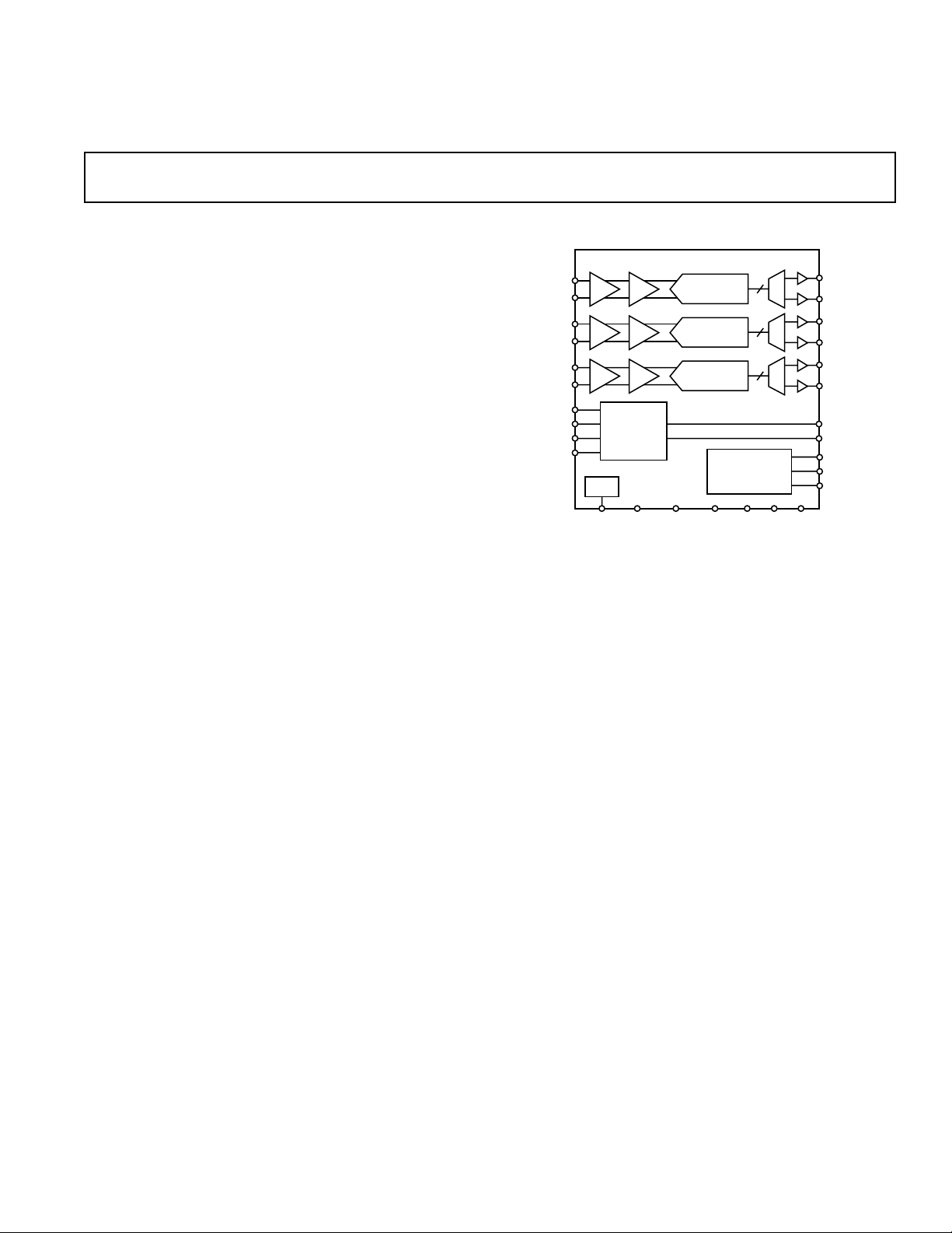
FUNCTIONAL BLOCK DIAGRAM
GENERAL DESCRIPTION
The AD9483 is a triple 8-bit monolithic analog-to-digital
converter optimized for digitizing RGB graphics signals from
personal computers and workstations. Its 140 MSPS encode
rate capability and full-power analog bandwidth of 330 MHz
supports display resolutions of up to 1280 × 1024 at 75 Hz with
sufficient input bandwidth to accurately acquire and digitize
each pixel.
To minimize system cost and power dissipation, the AD9483
includes an internal +2.5 V reference and track-and-hold circuit. The user provides only a +5 V power supply and an encode clock. No external reference or driver components are
required for many applications. The digital outputs are threestate CMOS outputs. Separate output power supply pins support interfacing with 3.3 V or 5 V logic.
The AD9483’s encode input interfaces directly to TTL, CMOS,
or positive-ECL logic and will operate with single-ended or
differential inputs. The user may select dual channel or single
channel digital outputs. The Dual Channel (demultiplexed)
REV. A
Information furnished by Analog Devices is believed to be accurate and
reliable. However, no responsibility is assumed by Analog Devices for its
use, nor for any infringements of patents or other rights of third parties
which may result from its use. No license is granted by implication or
otherwise under any patent or patent rights of Analog Devices.
mode interleaves ADC data through two 8-bit channels at onehalf the clock rate. Operation in Dual Channel mode reduces
the speed and cost of external digital interfaces while allowing
the ADCs to be clocked to the full 140 MSPS conversion rate.
In the Single Channel mode, all data is piped at the full clock
rate to the Channel A outputs and the ADCs conversion rate is
limited to 100 MSPS. A data clock output is provided at the
Channel A output data rate for both Dual-Channel or SingleChannel output modes.
Fabricated in an advanced BiCMOS process, the AD9483 is
provided in a space-saving 100-lead MQFP surface mount plas-
tic package (S-100) and is specified over the 0°C to +85°C
temperature range.
One Technology Way, P.O. Box 9106, Norwood, MA 02062-9106, U.S.A.
Tel: 781/329-4700 World Wide Web Site: http://www.analog.com
Fax: 781/326-8703 © Analog Devices, Inc., 1998

(VCC = +5 V, VDD = +3.3 V, external reference, ENCODE = maximum conversion rate
AD9483–SPECIFICATIONS
differential PECL)
Test AD9483KS-140 AD9483KS-100
Parameter Temperature Level Min Typ Max Min Typ Max Units
RESOLUTION 8 8 Bits
DC ACCURACY
Differential Nonlinearity +25°C I 0.8 1.25/–1.0 0.8 1.25/–1.0 LSB
Full VI 1.50/–1.0 1.50/–1.0 LSB
Integral Nonlinearity +25°C I 0.9 1.50/–1.50 0.9 1.50/–1.50 LSB
Full VI 1.75/–1.75 1.75/–1.75 LSB
No Missing Codes Full VI Guaranteed Guaranteed
Gain Error
Gain Tempco
1
1
+25°CI ±1 ±2 ±1 ±2% FS
Full V 160 160 ppm/°C
ANALOG INPUT
Input Voltage Range
(With Respect to AIN) Full V ±512 ±512 mV p–p
Compliance Range AIN or AIN Full V 1.8 3.2 1.8 3.2 V
Input Offset Voltage +25°CI ±4 ±16 ±4 ±16 mV
Full VI ±20 ±20 mV
Input Resistance +25°C I 35 83 35 83 kΩ
Full VI 25 25 kΩ
Input Capacitance +25°CV 4 4 pF
Input Bias Current +25°C I 17 36 17 36 µA
Full VI 50 50 µA
Analog Bandwidth, Full Power +25°C V 330 330 MHz
REFERENCE OUTPUT
Output Voltage Full VI +2.4 +2.5 +2.6 +2.4 +2.5 +2.6 V
Temperature Coefficient Full V 110 110 ppm/°C
SWITCHING PERFORMANCE
Maximum Conversion Rate Full VI 140 100 MSPS
Minimum Conversion Rate Full IV 10 10 MSPS
Encode Pulsewidth High (t
Encode Pulsewidth Low (t
Aperture Delay (t
) +25°C V 1.5 1.5 ns
A
) +25°C IV 2.8 50 4.0 50 ns
EH
) +25°C IV 2.8 50 4.0 50 ns
EL
Aperture Delay Matching +25°C V 100 100 ps
Aperture Uncertainty (Jitter) +25°C V 2.3 2.3 ps rms
Data Sync Setup Time (t
Data Sync Hold Time (t
Data Sync Pulsewidth (t
Output Valid Time (t
Output Propagation Delay (t
Clock Valid Time (t
CV
Clock Propagation Delay (t
Data to Clock Skew (t
Data to Clock Skew (tPD–t
) +25°CIV0 0 ns
SDS
) +25°C IV 0.5 0.5 ns
HDS
) +25°C IV 2.0 2.0 ns
PWDS
2
)
V
PD
3
)
CPD
) Full VI –1.0 0 1.0 –1.0 0 1.0 ns
V–tCV
) Full VI –2.0 0 2.0 –2.0 0 2.0 ns
CPD
Full VI 4.0 6.3 4.0 6.3 ns
2
)
Full VI 8.0 10 8.0 10 ns
Full VI 3.8 6.2 3.8 6.2 ns
3
)
Full VI 8.0 10 8.0 10 ns
DIGITAL INPUTS
Input Capacitance +25°CV 3 3 pF
DIFFERENTIAL INPUTS
Differential Signal Amplitude (VID) Full IV 400 400 mV
HIGH Input Voltage (V
LOW Input Voltage (V
Common-Mode Input (V
HIGH Level Current (I
) Full IV 0.4 V
IHD
) Full IV 0 0 V
ILD
) Full IV 1.5 1.5 V
ICM
) Full VI 1.2 1.2 mA
IH
CC
0.4 V
CC
V
LOW Level Current (IIL) Full VI 1.2 1.2 mA
VREF IN
Input Resistance +25°C V 2.5 2.5 kΩ
–2–
REV. A

AD9483
Test AD9483KS-140 AD9483KS-100
Parameter Temperature Level Min Typ Max Min Typ Max Units
SINGLE-ENDED INPUTS
HIGH Input Voltage (VIH) Full IV 2.0 V
LOW Input Voltage (V
HIGH Level Current (I
) Full IV 0 0.8 0 0.8 V
IL
) Full VI 1 1 mA
IH
CC
LOW Level Current (IIL) Full VI 1 1 mA
DIGITAL OUTPUTS
Logic “1” Voltage Full VI V
– 0.05 V
DD
Logic “0” Voltage Full VI 0.05 0.05 V
Output Coding Binary Binary
POWER SUPPLY
VCC Supply Current Full VI 215 215 mA
V
Supply Current Full VI 60 60 mA
DD
Total Power Dissipation
4
Full VI 1.0 1.3 1.0 1.3 W
Power-Down Supply Current +25°CV 420 420mA
Power-Down Dissipation +25°C V 20 100 20 100 mW
DYNAMIC PERFORMANCE
5
Transient Response +25°C V 1.5 1.5 ns
Overvoltage Recovery Time +25°C V 1.5 1.5 ns
Signal-to-Noise Ratio (SNR)
(Without Harmonics)
= 19.7 MHz +25°C V 45 45 dB
f
IN
f
= 49.7 MHz +25°C I 41 44 41 44 dB
IN
f
= 69.7 MHz +25°C V 44 44 dB
IN
Signal-to-Noise Ratio (SINAD)
(With Harmonics)
= 19.7 MHz +25°C V 44 44 dB
f
IN
= 49.7 MHz +25°C I 40 43 40 43 dB
f
IN
f
= 69.7 MHz +25°C V 42 42 dB
IN
Effective Number of Bits
= 19.7 MHz +25°C V 7.0 7.0 Bits
f
IN
f
= 49.7 MHz +25°C I 6.4 6.8 6.4 6.8 Bits
IN
f
= 69.7 MHz +25°C V 6.8 6.8 Bits
IN
2nd Harmonic Distortion
= 19.7 MHz +25°C V 63 63 dBc
f
IN
f
= 49.7 MHz +25°C I 50 58 50 58 dBc
IN
= 69.7 MHz +25°C V 51 51 dBc
f
IN
3rd Harmonic Distortion
f
= 19.7 MHz +25°C V 56 56 dBc
IN
= 49.7 MHz +25°C I 46 54 46 54 dBc
f
IN
f
= 69.7 MHz +25°C V 51 51 dBc
IN
Crosstalk Full V 55 55 dB
NOTES
1
Gain error and gain temperature coefficient are based on the ADC only (with a fixed +2.5 V external reference).
2
tV and t
3
tCV and t
4
Measured under the following conditions: analog input is –1 dBFS at 19.7 MHz.
5
SNR/harmonics based on an analog input voltage of –1.0 dBFS referenced to a 1.024 V full-scale input range.
Typical thermal impedance for the S-100 (MQFP) 100-lead package: θJC = 10°C/W, θCA = 17°C/W, θJA = 27°C/W.
Specifications subject to change without notice.
are measured from the threshold crossing of the ENCODE input to valid TTL levels at the digital outputs. The output ac load during test is 5 pF.
PDF
are measured from the threshold crossing of the ENCODE input to valid TTL levels at the digital outputs. The output ac load during test is 20 pF.
CPD
2.0 V
– 0.05 V
DD
CC
V
–3–REV. A
AD9483
WARNING!
ESD SENSITIVE DEVICE
ABSOLUTE MAXIMUM RATINGS*
VCC . . . . . . . . . . . . . . . . . . . . . . . . . . . . . . . . . . . . . . . . . +6 V
. . . . . . . . . . . . . . . . . . . . . . . . . . . . . . . . . . . . . . . . . +6 V
V
DD
Analog Inputs . . . . . . . . . . . . . . . . . . . . . . . . . . . V
VREF IN, VREF OUT . . . . . . . . . . . . . . . . . . . . V
Digital Inputs . . . . . . . . . . . . . . . . . . . . . . . . . . . V
to 0.0 V
CC
to 0.0 V
CC
to 0.0 V
CC
Digital Output Current . . . . . . . . . . . . . . . . . . . . . . . . 20 mA
Operating Temperature . . . . . . . . . . . . . . . . . . . 0°C to +85°C
Storage Temperature . . . . . . . . . . . . . . . . . . –65°C to +150°C
Maximum Junction Temperature . . . . . . . . . . . . . . . . +175°C
Maximum Case Temperature . . . . . . . . . . . . . . . . . . .+150°C
*Stresses above those listed under Absolute Maximum Ratings may cause perma-
nent damage to the device. This is a stress rating only; functional operation of the
device at these or any other conditions above those indicated in the operational
sections of this specification is not implied. Exposure to absolute maximum ratings
for extended periods may effect device reliability.
EXPLANATION OF TEST LEVELS
Test Level
I – 100% production tested.
II – 100% production tested at +25°C and sample tested at
specified temperatures.
III – Periodically sample tested.
IV – Parameter is guaranteed by design and characterization
testing.
V – Parameter is a typical value only.
VI – 100% production tested at +25°C; guaranteed by design
and characterization testing.
Table I. Output Coding
Step AIN–AIN Code Binary
255 ≥0.512 V 255 1111 1111
254 0.508 V 254 1111 1110
253 0.504 V 253 1111 1101
•• • •
•• • •
•• • •
129 0.006 V 129 1000 0001
128 0.002 V 128 1000 0000
127 –0.002 V 127 0111 1111
126 –0.006 V 126 0111 1110
•• • •
•• • •
•• • •
2 –0.504 V 2 0000 0010
1 –0.508 V 1 0000 0001
0 ≤–0.512 V 0 0000 0000
ORDERING GUIDE
Temperature Package Package
Model Range Description Option
AD9483KS-100 0°C to +85°C Plastic Thin Quad Flatpack S-100B
AD9483KS-140 0°C to +85°C Plastic Thin Quad Flatpack S-100B
AD9483/PCB +25°C Evaluation Board
CAUTION
ESD (electrostatic discharge) sensitive device. Electrostatic charges as high as 4000 V readily
accumulate on the human body and test equipment and can discharge without detection.
Although the AD9483 features proprietary ESD protection circuitry, permanent damage may
occur on devices subjected to high energy electrostatic discharges. Therefore, proper ESD
precautions are recommended to avoid performance degradation or loss of functionality.
–4–
REV. A
AD9483
PIN FUNCTION DESCRIPTIONS
Pin Number Name Function
1, 6, 7, 10, 20, 30, 40, 50,
60, 70, 73, 77, 78, 80, 81,
95, 96, 100 GND Ground
2 ENCODE Encode clock for ADC (ADC samples on rising edge of ENCODE).
3 ENCODE Encode clock complement (ADC samples on falling edge of ENCODE).
4 DS Data Sync Aligns output channels in Dual-Channel mode.
5 DS Data Sync complement.
8 DCO Data Clock Output. Clock output at Channel A data rate.
9 DCO Data Clock Output complement.
11, 21, 31, 41, 51, 61, 71 V
79, 82, 83, 93, 94, 98, 99 V
12–19 D
22–29 D
32–39 D
42–49 D
52–59 D
62–69 D
DD
CC
BB7–DBB0
BA7–DBA0
GB7–DGB0
GA7–DGA0
RB7–DRB0
RA7–DRA0
72 NC No Connect.
74 OMS Selects Single Channel or Dual Channel output mode, (HIGH = single,
75 I/P Selects interleaved or parallel output mode, (HIGH = interleaved, LOW = parallel).
76 PD Power-Down and Three-State Select (HIGH = power-down).
84 R AIN Analog Input Complement for Converter “R.”
85 R AIN Analog Input True for Converter “R.”
86 R REF IN Reference Input for Converter “R” (+2.5 V Typical, ±10%).
87 G AIN Analog Input Complement for Converter “G.”
88 G AIN Analog Input True for Converter “G.”
89 G REF IN Reference Input for Converter “G” (+2.5 V Typical, ±10%).
90 B AIN Analog Input Complement for Converter “B.”
91 B AIN Analog Input True for Converter “B.”
92 B REF IN Reference Input for Converter “B” (+2.5 V Typical, ±10%).
97 REF OUT Internal Reference Output (+2.5 V Typical); Bypass with 0.01 µF to Ground.
Output Power Supply. Nominally 3.3 V.
Converter Power Supply. Nominally 5.0 V.
Digital Outputs of Converter “B,” Channel B. DBB7 is the MSB.
Digital Outputs of Converter “B,” Channel A. DBA7 is the MSB.
Digital Outputs of Converter “G,” Channel B. DGB7 is the MSB.
Digital Outputs of Converter “G,” Channel A. DGA7 is the MSB.
Digital Outputs of Converter “R,” Channel B. DRB7 is the MSB.
Digital Outputs of Converter “R,” Channel A. DRA7 is the MSB.
LOW = demuxed).
–5–REV. A
AD9483
GND
1
GND
GND
DCO
DCO
GND
V
DBB
DBB
DBB
DBB
DBB
DBB
DBB
DBB
GND
V
DBA
DBA
DBA
DBA
DBA
DBA
DBA
DBA
GND
DS
DS
2
3
4
5
6
7
8
9
10
11
DD
12
7
13
6
14
5
15
4
16
3
17
2
18
1
19
0
20
21
DD
22
7
23
6
24
5
25
4
26
3
27
2
28
1
29
0
30
ENCODE
ENCODE
NC = NO CONNECT
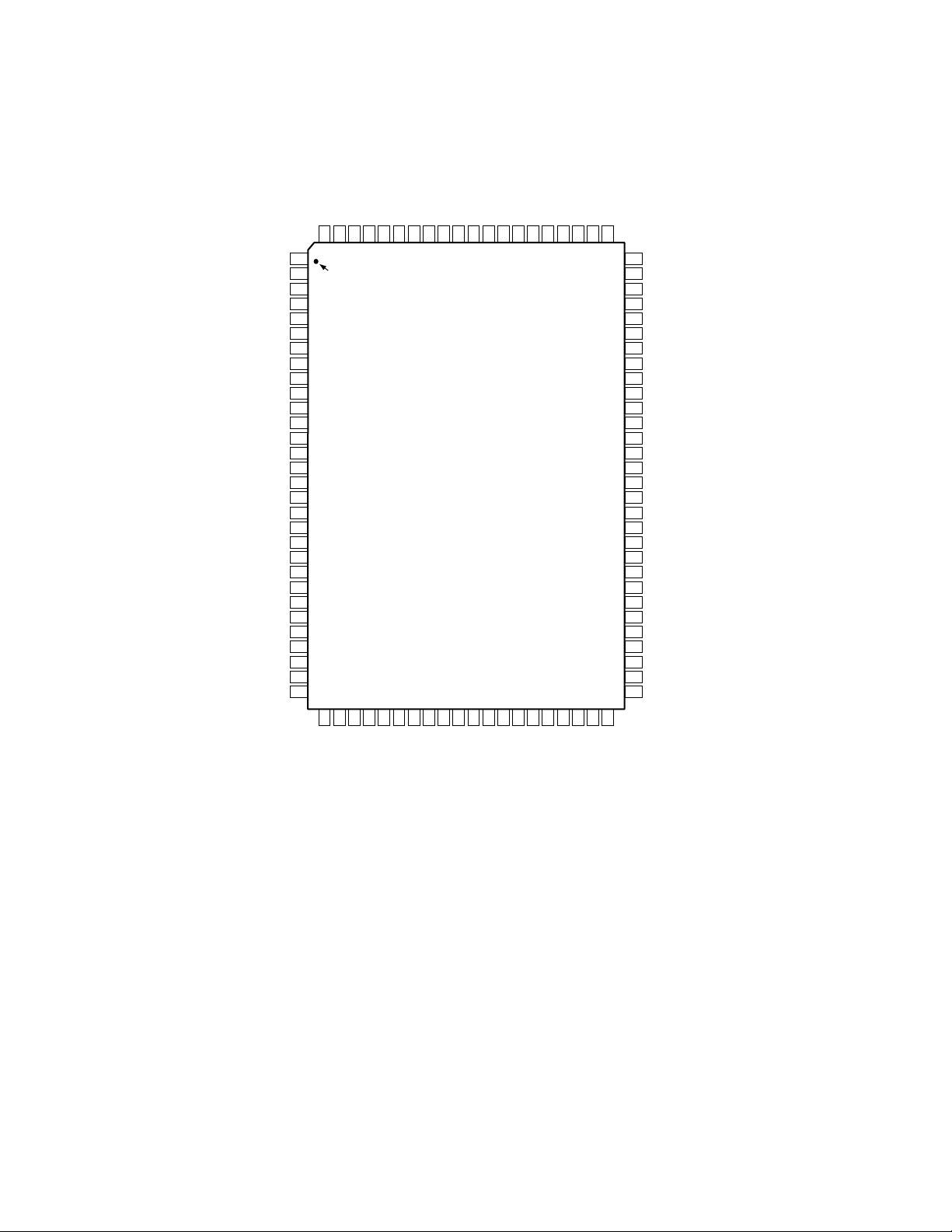
PIN CONFIGURATION
Plastic Thin Quad Flatpack (S-100B)
CC
CC
V
V
GND
100
PIN 1
IDENTIFIER
GND
REF OUT
99989796959493
GND
CC
CC
B AIN
V
V
B REF IN
929190
B AIN
G REF IN
G AIN
89
88
G AIN
R REF IN
8786858483
AD9483
TOP VIEW
(PINS DOWN)
31
33
32
7
6
B
B
DD
G
G
V
D
D
37
35
34
5
4
B
B
G
G
D
D
39
40
38
36
3
2
B
B
G
G
D
D
41
1
0
B
B
DD
G
G
V
GND
D
D
45
43
44
42
7
6
5
A
D
4
A
A
A
G
G
G
G
D
D
D
R AIN
46
3
A
G
D
R AIN
47
2
A
G
D
CC
CC
GND
V
V
81
82
80
GND
79
V
CC
78
GND
77
GND
76
PD
75
I/P
74
OMS
73
GND
72
NC
71
V
DD
70
GND
69
DRA
0
68
DRA
1
67
DRA
2
66
DRA
3
65
DRA
4
64
DRA
5
63
DRA
6
62
DRA
7
61
V
DD
60
GND
59
DRB
0
58
DRB
1
57
DRB
2
56
DRB
3
55
DRB
4
54
DRB
5
DRB
53
6
52
DRB
7
51
V
DD
50
49
48
1
0
A
A
G
G
GND
D
D
–6–
REV. A
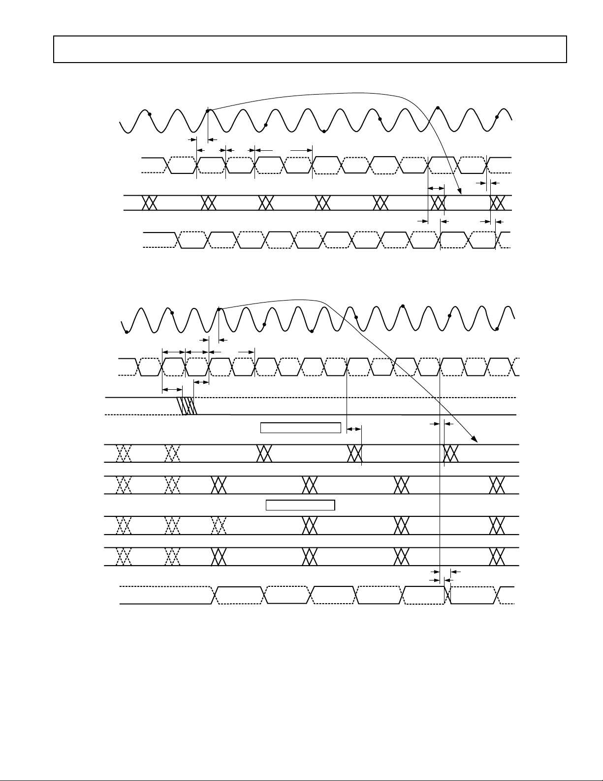
TIMING
AD9483
AIN
ENCODE
ENCODE
DS
AIN
ENCODE
ENCODE
D7–D0
CLOCK OUT
CLOCK OUT
SAMPLE N–2
SAMPLE N–1
SAMPLE N
t
EH
SAMPLE N+3
A
SAMPLE N+1
t
EL
1/f
t
SAMPLE N+2
S
SAMPLE N+4
t
DATA N–5 DATA N–4 DATA N–3 DATA N–2 DATA N–1 DATA N
t
CPD
Figure 1. Timing—Single Channel Mode
SAMPLE N–1
t
EH
t
HDS
t
EL
t
SDS
SAMPLE N
t
A
1/f
SAMPLE N+1
S
SAMPLE N+2
SAMPLE N+3
SAMPLE N+4
SAMPLE N+5
PD
t
V
t
CV
SAMPLE N+6
DS
PORT A
D7–D0
PORT B
D7–D0
PORT A
D7–D0
PORT B
D7–D0
CLKOUT
CLKOUT
DATA N–7
OR N–8
DATA N–8
OR N–7
DATA N–9
OR N–8
DATA N–8
OR N–7
DATA N–7
DATA N–6
OR N–7
DATA N–7
OR N–8
DATA N–6
OR N–7
INTERLEAVED DATA OUT
OR N–6
INVALID IF OUT OF SYNC
DATA N–5 IF IN SYNC
INVALID IF OUT OF SYNC
DATA N–5 IF IN SYNC
INVALID IF OUT OF SYNC
DATA N–4 IF IN SYNC
PARALLEL DATA OUT
DATA N–7
OR N–6
DATA N–3
INVALID IF OUT OF SYNC
DATA N–4 IF IN SYNC
DATA N–3
Figure 2. Timing—Dual Channel Mode
t
PD
DATA N–2
t
V
DATA N
DATA N–1
DATA N–2
DATA N–1
t
t
CV
CPD
DATA N+1
DATA N
DATA N+1
–7–REV. A
AD9483
V
DD
DIGITAL
OUTPUTS
AD9483
V
CC
AD9483
DIGITAL
INPUTS
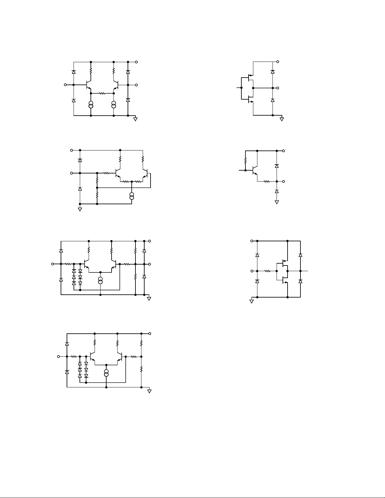
EQUIVALENT CIRCUITS
V
CC
AIN
AIN
AD9483
Figure 3. Equivalent Analog Input Circuit
V
CC
VREF IN
500V
2kV
AD9483
Figure 4. Equivalent Reference Input Circuit
17.5kV
ENCODE
300V
DS
AD9483
300V
7.5kV
V
CC
ENCODE
DS
Figure 7. Equivalent Digital Output Circuit
V
CC
VREF
OUT
AD9483
Figure 8. Equivalent Reference Output Circuit
Figure 5. Equivalent Encode and Data Select Input Circuit
V
AD9483
DEMUX
Input Circuit
DEMUX
Figure 6. Equivalent
Figure 9. Equivalent Digital Input Circuit
CC
–8–
REV. A
 Loading...