Analog Devices AD9433BSQ-125, AD9433BSQ-105, AD9433-PCB Datasheet
12-Bit, 105 MSPS/125 MSPS
V
CC
AIN
AIN
ENCODE
ENCODE
REF
OUT
REF
IN
GND
V
DD
D11–D0
DFS
SFDR
12
12
PIPELINE
ADC
T/H
ENCODE
TIMING
REF
OUTPUT
STAGING
AD9433
a
FEATURES
IF Sampling up to 350 MHz
SNR = 67.5 dB, f
SFDR = 83 dBc, f
SFDR = 72 dBc, f
2 V p-p Analog Input Range Option
On-Chip Clock Duty Cycle Stabilization
On-Chip Reference and Track/Hold
SFDR Optimization Circuit
Excellent Linearity:
DNL = 0.25 LSB (Typ)
INL = 0.5 LSB (Typ)
750 MHz Full Power Analog Bandwidth
Power Dissipation = 1.35 W Typical @ 125 MSPS
Two’s Complement or Offset Binary Data Format
5.0 V Analog Supply Operation
2.5 V to 3.3 V TTL/CMOS Outputs
APPLICATIONS
Cellular Infrastructure Communication Systems
3G Single and Multicarrier Receivers
IF Sampling Schemes
Wideband Carrier Frequency Systems
Point to Point Radios
LMDS, Wireless Broadband
MMDS Base Station Units
Cable Reverse Path
Communications Test Equipment
Radar and Satellite Ground Systems
GENERAL INTRODUCTION
The AD9433 is a 12-bit monolithic sampling analog-to-digital
converter with an on-chip track-and-hold circuit and
for ease of use. The product operates up to
sion rate and is optimized for outstanding dynamic performance
in wideband and high IF carrier systems.
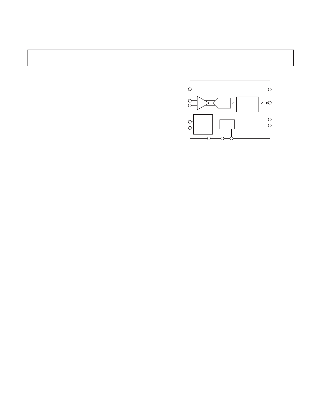
The ADC requires a 5 V analog power supply and a differential
encode clock for full performance operation. No external reference or driver components are required for many applications.
The digital outputs are TTL/CMOS compatible and a separate
output power supply pin supports interfacing with 3.3 V or
2.5 V logic.
A user-selectable, on-chip proprietary circuit optimizes spuriousfree dynamic range (SFDR) versus signal-to-noise-and-distortion
(SINAD) ratio performance for different input signal frequencies,
providing as much as 83 dBc SFDR performance over the dc
to 70 MHz band.
up to Nyquist @ 105 MSPS
IN
70 MHz @ 105 MSPS
IN
150 MHz @ 105 MSPS
IN
125 MSPS conver-
is designed
IF Sampling A/D Converter
AD9433
FUNCTIONAL BLOCK DIAGRAM
The encode clock supports either differential or single-ended
input and is PECL-compatible. The output format is userselectable for binary or two’s complement and provides an
overrange (OR) signal.
Fabricated on an advanced BiCMOS process, the AD9433 is
available in a thermally enhanced 52-lead plastic quad flatpack
specified over the industrial temperature
+85°C) and is pin-compatible with the AD9432.
PRODUCT HIGHLIGHTS
1. IF Sampling
The AD9433 maintains outstanding ac performance up to
input frequencies of 350 MHz. Suitable for 3G Wideband
Cellular IF sampling receivers.
2. Pin-Compatibility
This ADC has the same footprint and pin layout as the
AD9432, 12-Bit 80/105 MSPS ADC.
3. SFDR Performance
A user-selectable on-chip circuit optimizes SFDR performance
as much at 85 dBc from dc to 70 MHz.
4. Sampling Rate
At 125 MSPS, this ADC is ideally suited for current wireless
and wired broadband applications such as LMDS/MMDS
and cable reverse path.
range (–40°C to
REV. 0
Information furnished by Analog Devices is believed to be accurate and
reliable. However, no responsibility is assumed by Analog Devices for its
use, nor for any infringements of patents or other rights of third parties that
may result from its use. No license is granted by implication or otherwise
under any patent or patent rights of Analog Devices.
One Technology Way, P.O. Box 9106, Norwood, MA 02062-9106, U.S.A.
Tel: 781/329-4700www.analog.com
Fax: 781/326-8703 © Analog Devices, Inc., 2001

AD9433–SPECIFICATIONS
DC SPECIFICATIONS
(VDD = 3.3 V, VCC = 5 V; internal reference; differential encode input, unless otherwise noted.)
◊
Test AD9433BSQ-105 AD9433BSQ-125
Parameter Temp Level Min Typ Max Min Typ Max Unit
RESOLUTION 12 12 Bits
ACCURACY
No Missing Codes Full VI Guaranteed Guaranteed
Offset Error Full VI –5 0 +5 –5 0 +5 mV
Gain Error
Differential Nonlinearity (DNL)
Integral Nonlinearity (INL)
1
2
2
25⬚CI –7 ⫾1+3 –7⫾1+3 % FS
25⬚C I –0.75 ⫾0.25 +0.75 –0.75 ⫾0.3 +0.75 LSB
Full VI –1 +1 –1 +1 LSB
25⬚C I –1.0 ⫾0.5 +1.0 –1.0 ⫾0.5 +1.0 LSB
Full VI –1.3 +1.3 –1.3 +1.3 LSB
THERMAL DRIFT
Offset Error Full V –50 –50 ppm/⬚C
Gain Error
1
Full V –125 –125 ppm/⬚C
Reference Full V ± 80 ±80 ppm/⬚C
REFERENCE
Internal Reference Volatge (VREFOUT) Full I 2.4 2.5 2.6 2.4 2.5 2.6 V
Output Current (VREFOUT) Full V 100 100 µA
Input Current (VREFIN) Full IV 50 50 µA
ANALOG INPUTS
Differential Input Voltage Range Full V 2.0 2.0 V
(AIN, AIN)
Common-Mode Voltage Full V 4.0 4.0 V
Input Resistance Full VI 2 3 4 2 3 4 kΩ
Input Capacitance Full V 4 4 pF
Analog Bandwidth, Full Power Full V 750 750 MHz
POWER SUPPLY
V
CC
V
DD
Power Dissipation
Power Supply Rejection Ratio (PSRR) 25⬚CI ⫾3 ⫾3 mV/V
2
IV
CC
2
IV
DD
3
Full IV 4.75 5.0 5.25 4.75 5.0 5.25 V
Full IV 2.7 3.3 2.7 3.3 V
Full VI 1275 1425 1350 1500 mW
Full VI 255 285 270 300 mA
Full VI 12.5 14 16 18 mA
ENCODE INPUTS
Internal Common-Mode Bias Full V 3.75 3.75 V
Differential Input (ENC – ENC) Full V 500 500 mV
Input Voltage Range Full IV –0.5 V
+ 0.05 –0.5 V
CC
+ 0.05 V
CC
Input Common-Mode Range Full IV 2.0 4.25 2.0 4.25 V
Input Resistance Full VI 6 6 kΩ
Input Capacitance 25⬚CV 3 3 pF
DIGITAL INPUTS
Input High Voltage Full I 2.0 2.0 V
Input Low Voltage Full I 0.8 0.8 V
Input High Current (VIN = 5 V) Full V 50 50 µA
Input Low Current (VIN = 0 V) Full V 50 50 µA
DIGITAL OUTPUTS
Logic “1” Voltage Full VI VDD – 0.05 VDD – 0.05 V
Logic “0” Voltage Full VI 0.05 0.05 V
Output Coding Two’s Complement or Offset Binary
NOTES
1
Gain error and gain temperature coefficients are based on the ADC only (with a fixed 2.5 V external reference and a 2 V p-p differential analog input).
2
SFDR disabled (SFDR = GND) for DNL and INL specifications.
3
Power dissipation measured with rated encode and a dc analog input (Outputs Static, I
Specifications subject to change without notice.
VDD
= 0). I
VCC
and I
measured with 10.3 MHz analog input @ –0.5 dBFS.
VDD
–2–
REV. 0

AD9433
AC SPECIFICATIONS
(VDD = 3.3 V, VCC = 5 V; differential encode input, unless otherwise noted.)
Test AD9433BSQ-105 AD9433BSQ-125
Parameter Temp Level Min Typ Max Min Typ Max Unit
DYNAMIC PERFORMANCE*
Signal-to-Noise Ratio (SNR)
(Without Harmonics)
= 10.3 MHz 25⬚C I 66.5 68.0 66.0 67.7 dB
f
IN
= 49 MHz 25⬚C I 65.5 67.5 64.0 66.0 dB
f
IN
= 70 MHz 25⬚C V 67.0 65.4 dB
f
IN
= 150 MHz 25⬚C V 65.4 62.0 dB
f
IN
= 250 MHz 25⬚C V 63.7 60.0 dB
f
IN
Signal-to-Noise Ratio and Distortion (SINAD)
(With Harmonics)
f
= 10.3 MHz 25⬚C I 66.0 68.0 65.0 67.0 dB
IN
= 49 MHz 25⬚C I 64.0 67.5 63.5 65.5 dB
f
IN
= 70 MHz 25⬚C V 66.9 64.5 dB
f
IN
= 150 MHz 25⬚C V 64.0 61.5 dB
f
IN
f
= 250 MHz 25⬚C V 61.2 57.7 dB
IN
Effective Number of Bits
f
= 10.3 MHz 25⬚C I 11.1 10.9 Bits
IN
= 49 MHz 25⬚C I 11.0 10.7 Bits
f
IN
= 70 MHz 25⬚C V 10.9 10.6 Bits
f
IN
= 150 MHz 25⬚C V 10.4 10.0 Bits
f
IN
f
= 250 MHz 25⬚C V 9.9 9.4 Bits
IN
2nd and 3rd Harmonic Distortion
= 10.3 MHz 25⬚C I –78 –85 –76 –85 dBc
f
IN
= 49 MHz 25⬚C I –73 –80 –72 –76 dBc
f
IN
= 70 MHz 25⬚C V –83 –78 dBc
f
IN
= 150 MHz 25⬚C V –72 –67 dBc
f
IN
f
= 250 MHz 25⬚C V –67 –65 dBc
IN
Worst Other Harmonic or Spur
(Excluding Second and Third)
= 10.3 MHz 25⬚C I –88 –92 –84 –90 dBc
f
IN
= 49 MHz 25⬚C I –82 –89 –82 –87 dBc
f
IN
= 70 MHz 25⬚C V –87 –85 dBc
f
IN
= 150 MHz 25⬚C V –87 –84 dBc
f
IN
f
= 250 MHz 25⬚C V –85 –76 dBc
IN
Two-Tone Intermod Distortion (IMD3)
= 49.3 MHz, f
f
IN1
f
= 150 MHz, f
IN1
*SNR/Harmonics based on an analog input voltage of –0.5 dBFS referenced to a 2 V full-scale input range. Harmonics are specified with the SFDR active
(SFDR = +5 V). SNR/SINAD specified with SFDR disabled (SFDR = Ground).
Specifications subject to change without notice.
= 50.3 MHz 25⬚C V –92 –90 dBc
IN2
= 151 MHz 25⬚C V –80 –76 dBc
IN2
SWITCHING SPECIFICATIONS
(VDD = 3.3 V, VCC = 5 V; differential encode input, unless otherwise noted.)
Test AD9433BSQ-105 AD9433BSQ-125
Parameter Temp Level Min Typ Max Min Typ Max Unit
Encode Rate Full IV 10 105 10 125 MSPS
Encode Pulsewidth High (t
Encode Pulsewidth Low (t
Aperture Delay (t
)25⬚C V 2.1 2.1 ns
A
Aperture Uncertainty (Jitter)
Output Valid Time (t
Output Propagation Delay (t
Output Rise Time (t
Output Fall Time (t
R
F
) Full IV 2.9 2.4 ns
EH
) Full IV 2.9 2.4 ns
EL
1
2
)
V
PD
2
)
25⬚C V 0.25 0.25 ps rms
Full VI 2.5 4.0 2.5 4.0 ns
Full VI 4.0 5.5 4.0 5.5 ns
) Full V 2.1 2.1 ns
) Full V 1.9 1.9 ns
Out of Range Recovery Time 25⬚CV 2 2 ns
Transient Response Time 25⬚CV 2 2 ns
Latency Full IV 10 10 Cycles
NOTES
1
Aperture uncertainty includes contribution of the AD9433, crystal clock reference, and encode drive circuit.
2
tV and tPD are measured from the transition points of the ENCODE input to the 50%/50% levels of the digital output swing. The digital output load during testing is
not to exceed an ac load of 10 pF or a dc current of 50 µA. Rise and fall times measured from 10% to 90%.
Specifications subject to change without notice.
REV. 0
–3–
AD9433
ABSOLUTE MAXIMUM RATINGS*
Parameter Min Max Unit
ELECTRICAL
VDD Voltage –0.5 +6.0 V
Voltage –0.5 +6.0 V
V
CC
Analog Input Voltage –0.5 V
Digital Input Voltage –0.5 V
+ 0.5 V
CC
+ 0.5 V
CC
Digital Output Current 20 mA
ENVIRONMENTAL
Operating Temperature
Range (Ambient) –40 +85 ⬚C
Maximum Junction
Temperature +150 ⬚C
Storage Temperature
Range (Ambient) –65 +125 ⬚C
*Stresses greater than those listed under Absolute Maximum Ratings may cause
permanent damage to the device. This is a stress rating only; functional operation
of the device at these or any other conditions above those indicated in the
operational section of this specification is not implied. Exposure to absolute
maximum rating conditions for extended periods may affect device reliability.
ORDERING GUIDE
THERMAL CHARCTERISTICS
Thermal Resitance
52-Lead PowerQuad® 4 LQFP_ED
= 25°C/W, Soldered Heat Sink, No Airflow
JA
= 33°C/W, Unsoldered Heat Sink, No Airflow
JA
= 2°C/W, Bottom of Package (Heat Sink)
JC
Simulated typical performance for 4-layer JEDEC board, horizontal orientation.
EXPLANATION OF TEST LEVELS
Test Level
I 100% production tested.
II 100% production tested at 25⬚C and guaranteed by design
and characterization at specified temperatures.
III Sample Tested Only
Parameter is guaranteed by design and characterization testing.
IV
V Parameter is a typical value only.
VI 100% production tested at 25⬚C and guaranteed by design
and characterization for industrial temperature range.
Model Temperature Range Package Description Package Option
AD9433BSQ-105 –40°C to +85°C (Ambient) 52-Lead Plastic Thermally Enhanced Quad Flatpack SQ-52
AD9433BSQ-125 –40°C to +85°C (Ambient) 52-Lead Plastic Thermally Enhanced Quad Flatpack SQ-52
AD9433/PCB 25°C Evaluation Board with AD9433BSQ-125
(Supports – 105 Evaluation)
CAUTION
ESD (electrostatic discharge) sensitive device. Electrostatic charges as high as 4000 V readily
accumulate on the human body and test equipment and can discharge without detection. Although
the AD9433 features proprietary ESD protection circuitry, permanent damage may occur on
devices subjected to high-energy electrostatic discharges. Therefore, proper ESD precautions are
recommended to avoid performance degradation or loss of functionality.
WARNING!
ESD SENSITIVE DEVICE
PowerQuad is a registered trademark of AMkor Technology, Inc.
–4–
REV. 0

AD9433
PIN FUNCTION DESCRIPTIONS
Pin Number Mnemonic Function
1, 3, 4, 9, 11, 33, 34, 35, 38, 39, 40, GND Analog Ground
43, 48, 51
2, 5, 6, 10, 36, 37, 44, 47, 52 V
CC
7 ENCODE Encode Clock for ADC-Complementary
8 ENCODE Encode Clock for ADC-True (ADC samples on rising edge of
14 OR Out of Range Output
15–20, 25–30 D11–D0 Digital Output
13, 22, 23, 32 V
DD
12, 21, 24, 31 DGND Digital Output Ground
41 DFS Data Format Select. Low = Two’s Complement, High = Binary;
42 SFDR MODE CMOS control pin that enables (SFDR MODE = 1), a proprietary
45 VREFIN Reference Input for ADC (2.5 V typical)
46 VREFOUT Internal Reference Output (2.5 V typical); bypass with 0.1 µF to
49 AIN Analog Input-True
50 AIN Analog Input-Complement
Analog Supply (5 V)
ENCODE)
Digital Output Power Supply (3 V)
Floats Low
circuit that may improve the spurious free dynamic range (SFDR)
performance of the AD9433. It is useful in applications where the
dynamic range of the system is limited by discrete spurious
frequency content caused by nonlinearities in the ADC transfer
function. SFDR MODE = 0 for normal operation; Floats Low.
Ground
GND
V
GND
GND
V
V
ENCODE
ENCODE
GND
V
GND
DGND
V
PIN CONFIGURATION
CC
V
GND
52 51 50 49 48 43 42 41 4047 46 45 44
1
PIN 1
2
CC
CC
CC
CC
DD
IDENTIFIER
3
4
5
6
7
8
9
10
11
12
13
14 15 16 17 18 19 20 21 22 23 24 25 26
OR
(MSB) D11
V
AIN
AIN
GND
AD9433BSQ
TOP VIEW
(Not to Scale)
D9D8D7
D10
CC
CC
V
VREFOUT
VREFIN
DD VDD
D6
V
DGND
GND
SFDR MODE
DFS
D5
DGND
GND
D4
39
38
37
36
35
34
33
32
31
30
29
28
27
GND
GND
V
CC
V
CC
GND
GND
GND
V
DD
DGND
D0 (LSB)
D1
D2
D3
REV. 0
–5–

AD9433
DEFINITIONS OF SPECIFICATIONS
Analog Bandwidth
The analog input frequency at which the spectral power of the
fundamental frequency (as determined by the FFT analysis) is
reduced by 3 dB.
Aperture Delay
The delay between the 50% point of the rising edge of the
ENCODE command and the instant at which the analog
input is sampled.
Aperture Uncertainty (Jitter)
The sample-to-sample variation in aperture delay.
Differential Analog Input Resistance, Differential Analog
Input Capacitance, and Differential Analog Input Impedance
The real and complex impedances measured at each analog
Integral Nonlinearity
The deviation of the transfer function from a reference line
measured in fractions of 1 LSB using a best fit straight line
determined by a least square curve fit.
Minimum Conversion Rate
The encode rate at which the SNR of the lowest analog signal
frequency drops by no more than 3 dB below the guaranteed limit.
Maximum Conversion Rate
The maximum encode rate at which parametric testing is performed.
Output Propagation Delay
The delay between a differential crossing of ENCODE and
ENCODE and the time when all output data bits are within
valid logic levels.
Noise (for Any Range within the ADC)
input port. The resistance is measured statically and the capacitance and differential input impedances are measured with a
network analyzer.
Differential Analog Input Voltage Range
The peak-to-peak differential voltage that must be applied to
the converter to generate a fullscale response. Peak differential voltage is computed by observing the voltage on a single
pin and subtracting the voltage from the other pin, which is
180 degrees out of phase. Peak to peak differential is computed
by rotating the inputs phase 180 degrees and taking the peak
measurement again. Then the difference is computed between
both peak measurements.
Differential Nonlinearity
The deviation of any code width from an ideal 1 LSB step.
Effective Number of Bits
The effective number of bits (ENOB) is calculated from the
measured SNR based on the equation:
SNR dB
MEASURED
ENOB
=
Encode Pulsewidth/Duty Cycle
–. +
176 20
.
602
log
Full - Scale
Input Amplitude
Amplitude
Pulsewidth high is the minimum amount of time that the
ENCODE
pulse should be left in logic “1” state to achieve
rated performance; pulsewidth low is the minimum time
ENCODE pulse should be left in low state. See timing implications of changing t
in text. At a given clock rate, these
ENCH
specs define an acceptable Encode duty cycle.
Full-Scale Input Power
Expressed in dBm. Computed using the following equation:
rms
Z
Gain
Power
Full Scale
2
V
FullScale
0 001
.
10
=
log
Gain error is the difference between the measured and ideal
full-scale input voltage range of the ADC.
Harmonic Distortion
Where Z is the input impedance, FS is the full scale of the device
for the frequency in question, SNR is the value for the particular
input level, and SIGNAL is the signal level within the ADC
reported in dB below full scale. This value includes both thermal
and quantization noise.
Power Supply Rejection Ratio
The ratio of a change in input offset voltage to a change in
power supply voltage.
Signal-to-Noise and Distortion (SINAD)
The ratio of the rms signal amplitude (set 1 dB below full scale)
to the rms value of the sum of all other spectral components,
including harmonics but excluding dc.
Signal-to-Noise Ratio (without Harmonics)
The ratio of the rms signal amplitude (set at 1 dB below full
scale) to the rms value of the sum of all other spectral compo-
nents, excluding the first five harmonics and dc.
Spurious-Free Dynamic Range (SFDR)
The ratio of the rms signal amplitude to the rms value of the peak
spurious spectral component. The peak spurious component
may or may not be a harmonic. May be reported in dBc (i.e.,
degrades as signal level is lowered), or dBFS (always related back
to converter full scale).
Two-Tone Intermodulation Distortion Rejection
The ratio of the rms value of either input tone (f1, f2) to the rms
value of the worst third order intermodulation product; reported
in dBc. Products are located at 2f
Two-Tone SFDR
The ratio of the rms value of either input tone (f1, f2) to the rms
value of the peak spurious component. The peak spurious component may or may not be an IMD product. May be reported in
dBc (i.e., degrades as signal level is lowered), or in dBFS (always
related back to converter full scale).
Worst Other Spur
The ratio of the rms signal amplitude to the rms value of the
worst spurious component (excluding the second and third
harmonic) reported in dBc.
The ratio of the rms signal amplitude fundamental frequency to
the rms signal amplitude of a single harmonic component (second,
third, etc.), reported in dBc.
V = Z 0.001 10
NOISE
××
FS – SNR – Signal
dBm dBc dBFS
– f2 and 2f2 – f1.
1
10
–6–
REV. 0
AD9433
V
CC
VREFIN
SAMPLE N–1
A
IN
ENCODE
ENCODE
D11–D0
DATA N–11
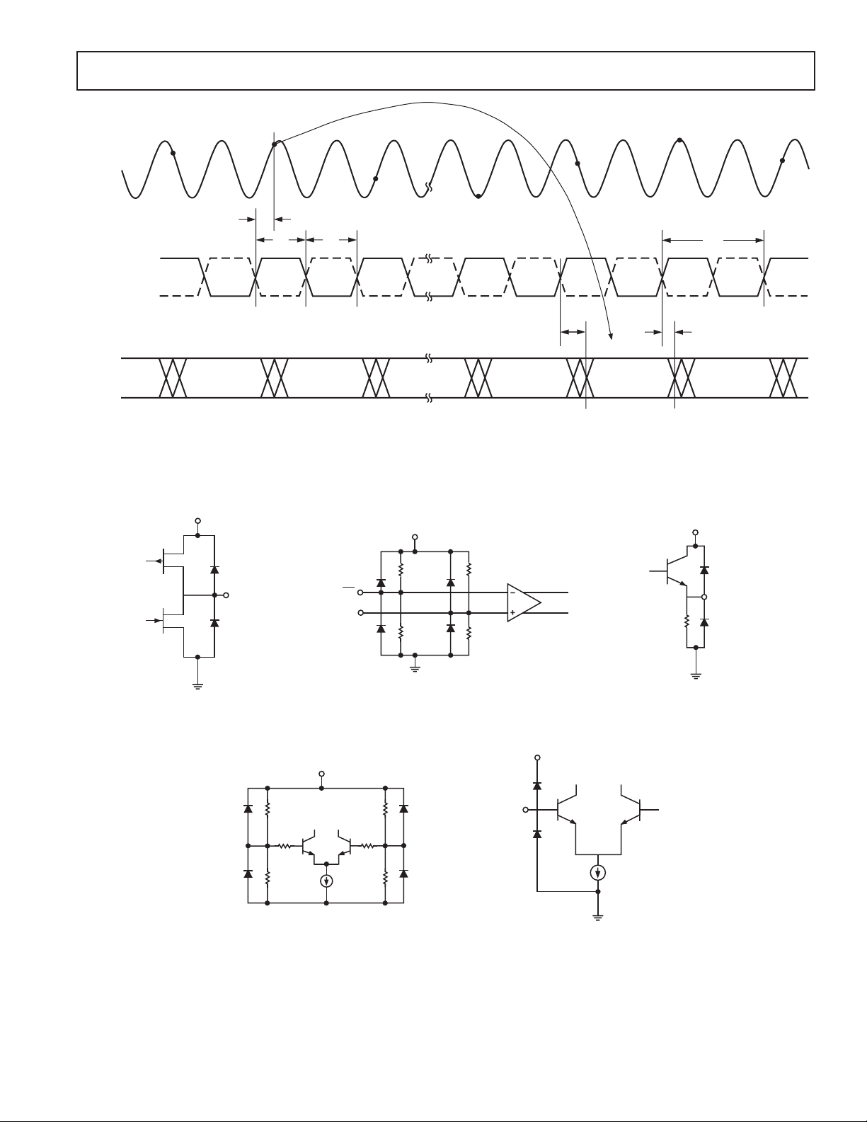
EQUIVALENT CIRCUITS
V
DD
SAMPLE N
t
A
t
EH
SAMPLE N+1 SAMPLE N+8
t
EL
DATA N–10
DATA
N–9
DATA
N–2
Figure 1. AD9433 Timing Diagram
V
CC
DATA N–1
SAMPLE N+9
t
PD
SAMPLE N+10
1/f
S
t
V
DATA N DATA N+1
V
CC
3.75k
D
X
Figure 2. Digital Output
8k
ENCODE
24k
Figure 5. Encode Inputs
AIN
AIN
15k
Figure 3. Analog Input
V
CC
8k
ENCODE
24k
3.75k
VREFOUT
15k
Figure 4. Reference Output
Figure 6. Reference Input
REV. 0
–7–
AD9433
AIN – Hz
60
050
SNR/SINAD – dB
100 150 200 250
61
62
63
64
65
66
67
SINAD
SNR
68
300
11.1
10.9
10.8
10.6
10.4
10.3
10.1
9.9
9.8
ENOBs – Bits
–Typical Performance Characteristics
0
SNR = 67.5dB
–10
SFDR = 85.0dBFS
–20
–30
–40
–50
–60
dB
–70
–80
–90
–100
–110
–120
0
13.1
26.3 39.4
FREQUENCY – MHz
52.5
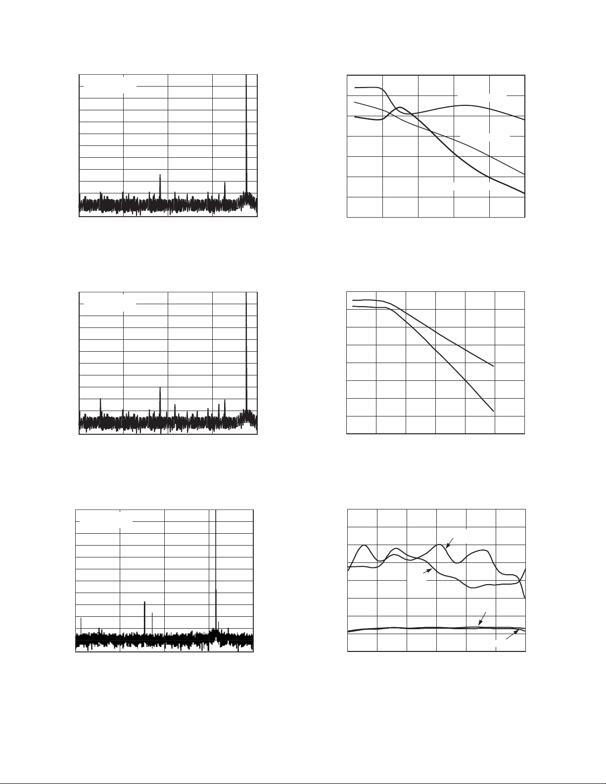
TPC 1. FFT: fS = 105 MSPS, fIN = 49.3 MHz, Differential
AIN @ –0.5 dBFS, SFDR Enabled
0
SNR = 68.0dB
–10
SFDR = 80.0dBFS
–20
–30
–40
–50
–60
dB
–70
–80
–90
–100
–110
–120
0
13.1
26.3 39.4
FREQUENCY – MHz
52.5
–95
–90
–85
–80
dBc
–75
–70
–65
–60
0
50
100 150 200 250
AIN – MHz
WORST OTHER
3RD HARMONIC
2ND HARMONIC
TPC 4. Harmonics (Second, Third, Worst Other) vs. AIN
Frequency. AIN @ –0.5 dBFS, f
= 105 MSPS, SFDR Enabled
S
TPC 2. FFT: fS = 105 MSPS, fIN = 49.3 MHz, Differential
AIN @ –0.5 dBFS, SFDR Disabled
0
SNR = 67.7dB
–10
SFDR = 76.0dBFS
–20
–30
–40
–50
–60
dB
–70
–80
–90
–100
–110
–120
0
TPC 3. FFT: fS = 125 MSPS, fIN = 49.3 MHz, Differential
FREQUENCY – MHz
AIN @ –0.5 dBFS, SFDR Enabled
46.831.215.6
62.5
–8–
TPC 5. SNR vs. AIN Frequency. Differential AIN @
–0.5 dBFS, 105 MSPS, SFDR Disabled
100
95
90
85
80
75
SNR/SINAD – dB
70
65
60
10 30
2ND
–dBc
50 70 90 110
ENCODE – MSPS
3RD
–dBc
SNR
SINAD
140
TPC 6. SNR/SINAD and Harmonic Distortion vs.
Encode Frequency. Differential AIN @ –0.5 dBFS
REV. 0
 Loading...