12-Bit, 105 MSPS/125 MSPS,
FEATURES
IF sampling up to 350 MHz
SNR: 67.5 dB, f
SFDR: 83 dBc, f
SFDR: 72 dBc, f
2 V p-p analog input range
On-chip clock duty cycle stabilization
On-chip reference and track-and-hold
SFDR optimization circuit
Excellent linearity
DNL: ±0.25 LSB (typical)
INL: ±0.5 LSB (typical)
750 MHz full power analog bandwidth
Power dissipation: 1.35 W (typical) at 125 MSPS
Twos complement or offset binary data format
5.0 V analog supply operation
2.5 V to 3.3 V T TL/CMOS outputs
APPLICATIONS
Cellular infrastructure communication systems
3G single- and multicarrier receivers
IF sampling schemes
Wideband carrier frequency systems
Point-to-point radios
LMDS, wireless broadband
MMDS base station units
Cable reverse path
Communications test equipment
Radar and satellite ground systems
GENERAL INTRODUCTION
The AD9433 is a 12-bit, monolithic sampling analog-to-digital
converter (ADC) with an on-chip track-and-hold circuit and is
designed for ease of use. The product operates up to a 125 MSPS
conversion rate and is optimized for outstanding dynamic performance in wideband and high IF carrier systems.
The ADC requires a 5 V analog power supply and a differential
encode clock for full performance operation. No external reference or driver components are required for many applications.
The digital outputs are TTL-/CMOS-compatible, and a separate
output power supply pin supports interfacing with 3.3 V or
2.5 V logic.
up to Nyquist at 105 MSPS
IN
= 70 MHz at 105 MSPS
IN
= 150 MHz at 105 MSPS
IN
IF Sampling ADC
AD9433
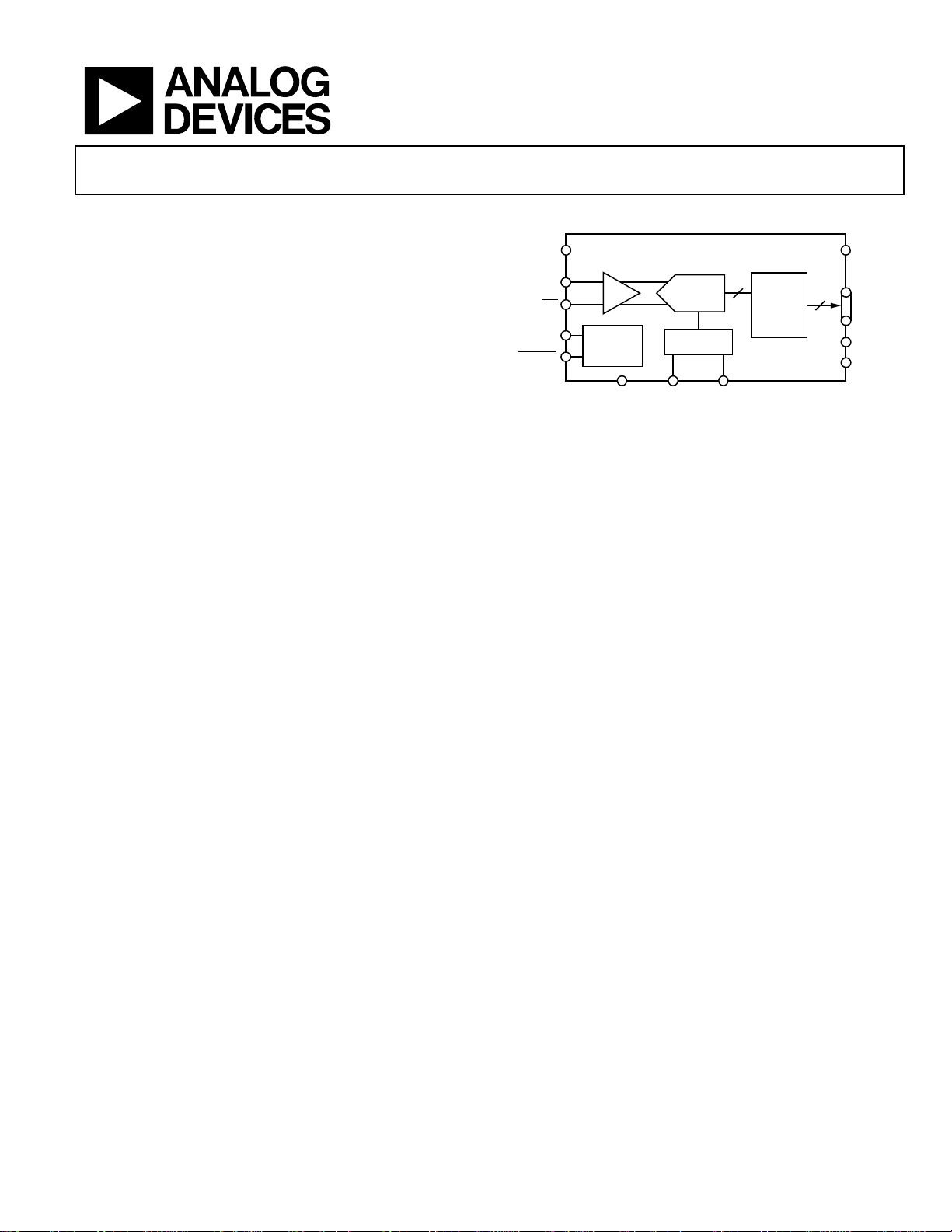
FUNCTIONAL BLOCK DIAGRAM
V
AIN
AIN
ENCODE
ENCODE
CC
T/H
ENCODE
TIMING
GND VREFOUT VREFIN
PIPELINE
ADC
REF
Figure 1.
12
AD9433
OUTPUT
STAGING
A user-selectable, on-chip proprietary circuit optimizes
spurious-free dynamic range (SFDR) vs. signal-to-noise and
distortion (SINAD) ratio performance for different input signal
frequencies, providing as much as 83 dBc SFDR performance
over the dc to 70 MHz band.
The encode clock supports either differential or single-ended
input and is PECL-compatible. The output format is userselectable for offset binary or twos complement and provides
an overrange (OR) signal.
Fabricated on an advanced BiCMOS process, the AD9433 is
available in a 52-lead thin quad flat package (TQFP_EP) that
is specified over the industrial temperature range of −40°C to
+85°C. The AD9433 is pin-compatible with the AD9432.
PRODUCT HIGHLIGHTS
1. IF Sampling.
The AD9433 maintains outstanding ac performance up to
input frequencies of 350 MHz. Suitable for 3G wideband
cellular IF sampling receivers.
2. Pin-Compatibility with the AD9432.
The AD9433 has the same footprint and pin layout as the
AD9432 12-bit 80 MSPS/105 MSPS ADC.
3. SFDR Performance.
A user-selectable, on-chip circuit optimizes SFDR
performance as much as 83 dBc from dc to 70 MHz.
4. Sampling Rate.
At 125 MSPS, the AD9433 is ideally suited for wireless and
wired broadband applications such as LMDS/MMDS and
cable reverse path.
V
DD
12
D11 TO D0
DFS
SFDR
MODE
01977-001
Rev. A
Information furnished by Analog Devices is believed to be accurate and reliable. However, no
responsibility is assumed by Analog Devices for its use, nor for any infringements of patents or other
rights of third parties that may result from its use. Specifications subject to change without notice. No
license is granted by implication or otherwise under any patent or patent rights of Analog Devices.
Trademarks and registered trademarks are the property of their respective owners.
One Technology Way, P.O. Box 9106, Norwood, MA 02062-9106, U.S.A.
Tel: 781.329.4700 www.analog.com
Fax: 781.461.3113 ©2001–2009 Analog Devices, Inc. All rights reserved.

AD9433
TABLE OF CONTENTS
Features .............................................................................................. 1
Applications ....................................................................................... 1
General Introduction ....................................................................... 1
Functional Block Diagram .............................................................. 1
Product Highlights ........................................................................... 1
Revision History ............................................................................... 2
Specifications ..................................................................................... 3
DC Specifications ......................................................................... 3
AC Specifications .......................................................................... 4
Switching Specifications .............................................................. 5
Timing Diagram ........................................................................... 5
Absolute Maximum Ratings ............................................................ 6
Explanation of Test Levels ........................................................... 6
Thermal Characteristics .............................................................. 6
ESD Caution .................................................................................. 6
Pin Configuration and Function Descriptions ............................. 7
Typical Performance Characteristics ..............................................8
Terminology .................................................................................... 14
Equivalent Circuits ......................................................................... 16
Theory of Operation ...................................................................... 17
Encode Input ............................................................................... 17
Encode Voltage Level Definition .............................................. 17
Analog Input ............................................................................... 18
SFDR Optimization.................................................................... 18
Digital Outputs ........................................................................... 18
Voltage Reference ....................................................................... 18
Timing ......................................................................................... 18
Applications Information .............................................................. 19
Layout Information .................................................................... 19
Replacing the AD9432 with the AD9433 ................................ 19
Outline Dimensions ....................................................................... 20
Ordering Guide .......................................................................... 20
REVISION HISTORY
6/09—Rev. 0 to Rev. A
Updated Format .................................................................. Universal
Reorganized Layout ............................................................ Universal
Added TQFP_EP Package ................................................. Universal
Deleted LQFP_ED Package ............................................... Universal
Changes to Thermal Characteristics Section ................................ 6
Changes to Pin Configuration and Function Descriptions
Section ................................................................................................ 7
Deleted Evaluation Board Section ................................................ 16
Updated Outline Dimensions ....................................................... 20
Changes to Ordering Guide .......................................................... 20
10/01—Revision 0: Initial Version
Rev. A | Page 2 of 20

AD9433
SPECIFICATIONS
DC SPECIFICATIONS
VDD = 3.3 V, VCC = 5 V; internal reference; differential encode input, unless otherwise noted.
Table 1.
Test 105 MSPS 125 MSPS
Parameter Temp Level Min Typ Max Min Typ Max Unit
RESOLUTION 12 12 Bits
ACCURACY
No Missing Codes Full VI Guaranteed Guaranteed
Offset Error Full VI −5 0 +5 −5 0 +5 mV
Gain Error
Differential Nonlinearity (DNL)225°C I −0.75 ±0.25 +0.75 −0.75 ±0.3 +0.75 LSB
Full VI −1 +1 −1 +1 LSB
Integral Nonlinearity (INL)
Full VI −1.3 +1.3 −1.3 +1.3 LSB
THERMAL DRIFT
Offset Error Full V −50 −50 ppm/°C
Gain Error
Reference Full V ±80 ±80 ppm/°C
REFERENCE
Internal Reference Voltage
Output Current (VREFOUT) Full V 100 100 μA
Input Current (VREFIN) Full IV 50 50 μA
ANALOG INPUTS (AIN, AIN)
Input Voltage Range Full V 2.0 2.0 V p-p
Common-Mode Voltage Full V 4.0 4.0 V
Input Resistance Full VI 2 3 4 2 3 4 kΩ
Input Capacitance Full V 4 4 pF
Analog Bandwidth, Full Power Full V 750 750 MHz
POWER SUPPLY
VCC Full IV 4.75 5.0 5.25 4.75 5.0 5.25 V
VDD Full IV 2.7 3.3 2.7 3.3 V
Power Dissipation
I
VCC
I
VDD
Power Supply Rejection Ratio
ENCODE INPUTS
Internal Common-Mode Bias Full V 3.75 3.75 V
Differential Input
Input Voltage Range Full IV −0.5 VCC + 0.05 −0.5 VCC + 0.05 V
Input Common-Mode Range Full IV 2.0 4.25 2.0 4.25 V
Input Resistance Full VI 6 6 kΩ
Input Capacitance 25°C V 3 3 pF
DIGITAL INPUTS
Input High Voltage Full I 2.0 2.0 V
Input Low Voltage Full I 0.8 0.8 V
Input High Current (VIN = 5 V) Full V 50 50 μA
Input Low Current (VIN = 0 V) Full V 50 50 μA
1
2
1
Full V −125 −125 ppm/°C
25°C I −7 ±1 +3 −7 ±1 +3 % FS
25°C I −1.0 ±0.5 +1.0 −1.0 ±0.5 +1.0 LSB
Full I 2.4 2.5 2.6 2.4 2.5 2.6 V
(VREFOUT)
3
3
3
Full VI 12.5 14 16 18 mA
Full VI 1275 1425 1350 1500 mW
Full VI 255 285 270 300 mA
25°C I ±3 ±3 mV/V
(PSRR)
Full V 500 500 mV
(ENCODE, ENCODE
)
Rev. A | Page 3 of 20

AD9433
Test 105 MSPS 125 MSPS
Parameter Temp Level Min Typ Max Min Typ Max Unit
DIGITAL OUTPUTS
Logic 1 Voltage Full VI VDD − 0.05 VDD − 0.05 V
Logic 0 Voltage Full VI 0.05 0.05 V
Output Coding Twos complement or offset binary Twos complement or offset binary
1
Gain error and gain temperature coefficients are based on the ADC only (with a fixed 2.5 V external reference and a 2 V p-p differential analog input).
2
SFDR mode disabled (SFDR MODE = GND) for DNL and INL specifications.
3
Power dissipation measured with rated encode and a dc analog input (outputs static, I
AC SPECIFICATIONS
VDD = 3.3 V, VCC = 5 V; differential encode input, unless otherwise noted.
Table 2.
Test 105 MSPS 125 MSPS
Parameter Temp Level Min Typ Max Min Typ Max Unit
DYNAMIC PERFORMANCE
Signal-to-Noise Ratio (SNR) (Without Harmonics)
fIN = 10.3 MHz 25°C I 66.5 68.0 66.0 67.7 dB
fIN = 49 MHz 25°C I 65.5 67.5 64.0 66.0 dB
fIN = 70 MHz 25°C V 67.0 65.4 dB
fIN = 150 MHz 25°C V 65.4 62.0 dB
fIN = 250 MHz 25°C V 63.7 60.0 dB
Signal-to-Noise and Distortion (SINAD) Ratio
(with Harmonics)
fIN = 10.3 MHz 25°C I 66.0 68.0 65.0 67.0 dB
fIN = 49 MHz 25°C I 64.0 67.5 63.5 65.5 dB
fIN = 70 MHz 25°C V 66.9 64.5 dB
fIN = 150 MHz 25°C V 64.0 61.5 dB
fIN = 250 MHz 25°C V 61.2 57.7 dB
Effective Number of Bits (ENOB)
fIN = 10.3 MHz 25°C I 11.1 10.9 Bits
fIN = 49 MHz 25°C I 11.0 10.7 Bits
fIN = 70 MHz 25°C V 10.9 10.6 Bits
fIN = 150 MHz 25°C V 10.4 10.0 Bits
fIN = 250 MHz 25°C V 9.9 9.4 Bits
Second-Order and Third-Order Harmonic
Distortion
fIN = 10.3 MHz 25°C I −78 −85 −76 −85 dBc
fIN = 49 MHz 25°C I −73 −80 −72 −76 dBc
fIN = 70 MHz 25°C V −83 −78 dBc
fIN = 150 MHz 25°C V −72 −67 dBc
fIN = 250 MHz 25°C V −67 −65 dBc
Worst Other Harmonic or Spur (Excluding
Second-Order and Third-Order Harmonics)
fIN = 10.3 MHz 25°C I −88 −92 −84 −90 dBc
fIN = 49 MHz 25°C I −82 −89 −82 −87 dBc
fIN = 70 MHz 25°C V −87 −85 dBc
fIN = 150 MHz 25°C V −87 −84 dBc
fIN = 250 MHz 25°C V −85 −76 dBc
Two-Tone Intermodulation Distortion (IMD3)
f
= 49.3 MHz; f
IN1
f
= 150 MHz; f
IN1
1
SNR/harmonics based on an analog input voltage of −0.5 dBFS referenced to a 2 V full-scale input range. Harmonics are specified with the SFDR mode enabled
(SFDR MODE = 5 V). SNR/SINAD specified with the SFDR mode disabled (SFDR MODE = ground).
1
= 50.3 MHz 25°C V −92 −90 dBc
IN2
= 151 MHz 25°C V −80 −76 dBc
IN2
VDD
= 0). I
VCC
and I
measured with 10.3 MHz analog input @ −0.5 dBFS.
VDD
Rev. A | Page 4 of 20

AD9433
SWITCHING SPECIFICATIONS
VDD = 3.3 V, VCC = 5 V; differential encode input, unless otherwise noted.
Table 3.
Test 105 MSPS 125 MSPS
Parameter Temp Level Min Typ Max Min Typ Max Unit
Encode Rate Full IV 10 105 10 125 MSPS
Encode Pulse Width High (tEH) Full IV 2.9 2.4 ns
Encode Pulse Width Low (tEL) Full IV 2.9 2.4 ns
Aperture Delay (tA) 25°C V 2.1 2.1 ns
Aperture Uncertainty (Jitter)
Output Valid Time (tV)
Output Propagation Delay (tPD)
Output Rise Time (tR)
Output Fall Time (tF)
2
Out-of-Range Recovery Time 25°C V 2 2 ns
Transient Response Time 25°C V 2 2 ns
Latency Full IV 10 10 Cycles
1
Aperture uncertainty includes contribution of the AD9433, crystal clock reference, and encode drive circuit.
2
tV and tPD are measured from the transition points of the ENCODE input to the 50%/50% levels of the digital output swing. The digital output load during testing is not
to exceed an ac load of 10 pF or a dc current of 50 μA. Rise and fall times are measured from 10% to 90%.
1
2
2
2
Full VI 4.0 5.5 4.0 5.5 ns
25°C V 0.25 0.25 ps rms
Full VI 2.5 4.0 2.5 4.0 ns
Full V 2.1 2.1 ns
Full V 1.9 1.9 ns
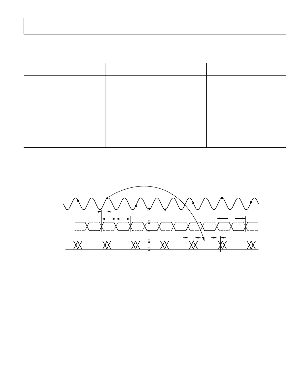
TIMING DIAGRAM
AIN
ENCODE
ENCODE
D11 TO D0
SAMPLE N – 1
DATA N – 11 DATA N – 10 DATA N – 1 DATA N DATA N + 1
SAMPLE N
t
A
SAMPLE N + 9
t
EL
EH
DATA
N – 9
SAMPLE N + 1
t
SAMPLE N + 8
DATA
N – 2
t
PD
SAMPLE N + 10
1/
t
V
f
S
01977-003
Figure 2. Timing Diagram
Rev. A | Page 5 of 20

AD9433
ABSOLUTE MAXIMUM RATINGS
Table 4.
Parameter Rating
VDD −0.5 V to +6.0 V
VCC −0.5 V to +6.0 V
Analog Inputs −0.5 V to VCC + 0.5 V
Digital Inputs −0.5 V to VDD + 0.5 V
Digital Output Current 20 mA
Operating Temperature Range (TA) −40°C to +85°C
Storage Temperature Range −65°C to +125°C
Maximum Junction Temperature (TJ) 150°C
Stresses above those listed under Absolute Maximum Ratings
may cause permanent damage to the device. This is a stress
rating only; functional operation of the device at these or any
other conditions above those indicated in the operational
section of this specification is not implied. Exposure to absolute
maximum rating conditions for extended periods may affect
device reliability.
EXPLANATION OF TEST LEVELS
I 100% production tested.
II 100% production tested at 25°C and sample tested at
specified temperatures.
III Sample tested only.
IV Parameter is guaranteed by design and characterization
testing.
V Parameter is a typical value only.
VI 100% production tested at 25°C; guaranteed by design and
characterization testing for industrial temperature range.
THERMAL CHARACTERISTICS
Table 5 lists AD9433 thermal characteristics for simulated typical
performance in a 4-layer JEDEC board, horizontal orientation.
Table 5. Thermal Resistance
Package Type θJA θ
52-Lead TQFP_EP (SV-52-2)1 2 °C/W
No Airflow 19.3 °C/W
1.0 m/s Airflow 16 °C/W
1
Bottom of package (exposed pad soldered to ground plane).
θJC Unit
JMA
ESD CAUTION
Rev. A | Page 6 of 20
 Loading...