

Page 1
12-Bit, 170/210 MSPS
FEATURES
SNR = 65 dB @ fIN = 70 MHz @ 210 MSPS
ENOB of 10.6 @ f
SFDR = 80 dBc @ f
Excellent linearity:
DNL = ±0.3 LSB (typical)
INL = ±0.5 LSB (typical)
2 output data options:
Demultiplexed 3.3 V CMOS outputs each @ 105 MSPS
Interleaved or parallel data output option
LVDS at 210 MSPS
700 MHz full-power analog bandwidth
On-chip reference and track-and-hold
Power dissipation = 1.3 W typical @ 210 MSPS
1.5 V input voltage range
3.3 V supply operation
Output data format option
Data sync input and data clock output provided
Clock duty cycle stabilizer
GENERAL DESCRIPTION
The AD9430 is a 12-bit, monolithic, sampling analog-to-digital
converter (ADC) optimized for high performance, low power,
and ease of use. The product operates up to a 210 MSPS
conversion rate and is optimized for outstanding dynamic
performance in wideband carrier and broadband systems. All
necessary functions, including a track-and-hold (T/H) and
reference, are included on the chip to provide a complete
conversion solution.
The ADC requires a 3.3 V power supply and a differential
ENCODE clock for full performance operation. The digital
outputs are TTL/CMOS or LVDS compatible and support either
twos complement or offset binary format. Separate output
power supply pins support interfacing with 3.3 V or 2.5 V
CMOS logic.
Two output buses support demultiplexed data up to 105 MSPS
rates in CMOS mode. A data sync input is supported for proper
output data port alignment in CMOS mode, and a data clock
output is available for proper output data timing. In LVDS
mode, the chip provides data at the ENCODE clock rate.
Fabricated on an advanced BiCMOS process, the AD9430 is
available in a 100-lead, surface-mount plastic package
(100 e-PAD TQFP) specified over the industrial temperature
range (–40°C to +85°C).
= 70 MHz @ 210 MSPS (–0.5 dBFS)
IN
= 70 MHz @ 210 MSPS (–0.5 dBFS)
IN
3.3 V A/D Converter
AD9430
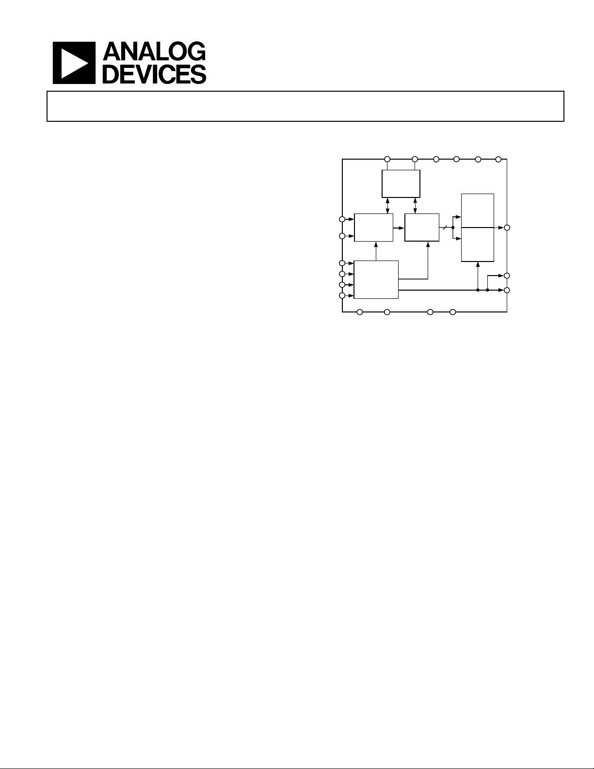
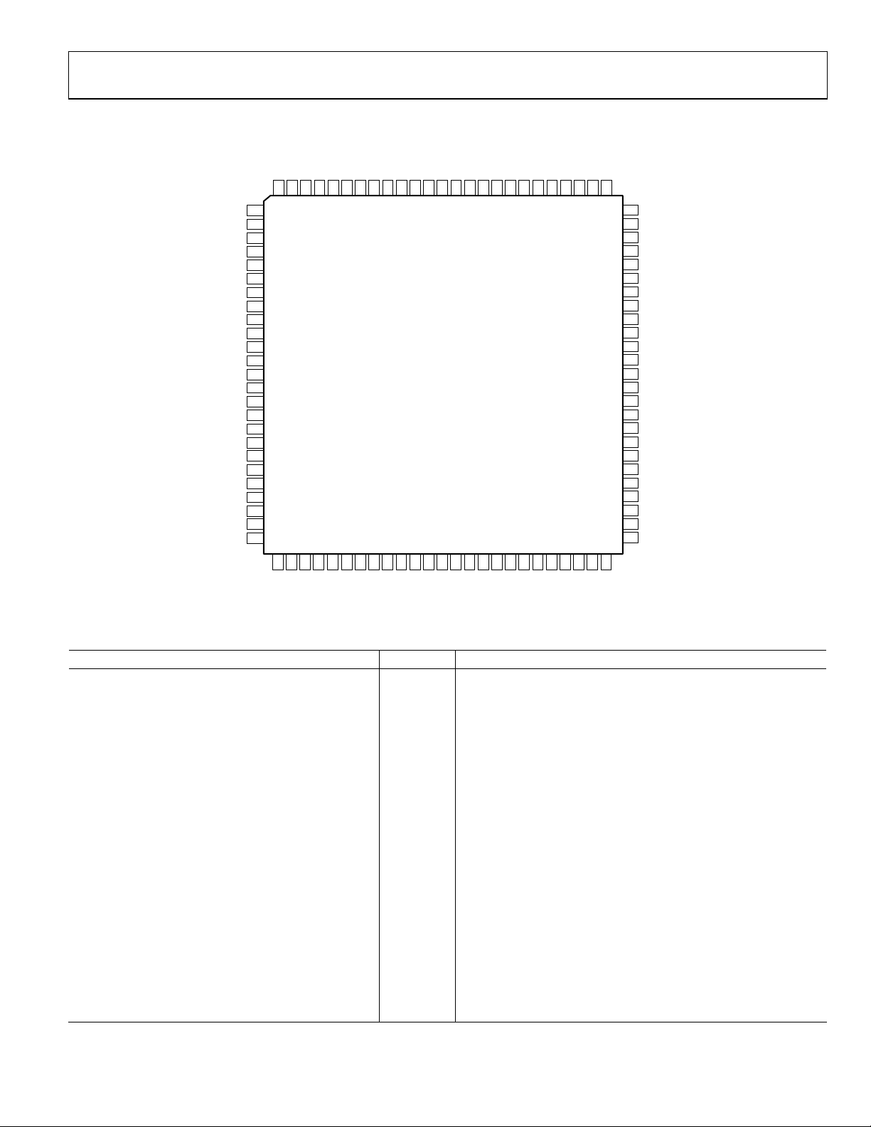
FUNCTIONAL BLOCK DIAGRAM
DRGND
12
OR LVDS
S5S4S2S1
DRVDD
LVDS
OUTPUTS
CMOS
OUTPUTS
AVDD
DATA,
OVERRANGE
IN LVDS OR
2-PORT CMOS
DCO+
DCO–
VIN+
VIN–
DS+
DS–
CLK+
CLK–
AD9430
TRACK-
AND-HOLD
CLOCK
MANAGEMENT
SENSE VREF
SCALABLE
REFERENCE
ADC
12-BIT
PIPELINE
CORE
AGND
SELECT CMOS
Figure 1.
APPLICATIONS
Wireless and wired broadband communications
Cable reverse path
Communications test equipment
Radar and satellite subsystems
Power amplifier linearization
PRODUCT HIGHLIGHTS
1. High performance.
Maintains 65 dB SNR @ 210 MSPS with a 65 MHz input.
2. Low power.
Consumes only 1.3 W @ 210 MSPS.
3. Ease of use.
LVDS output data and output clock signal allow interface
to current FPGA technology. The on-chip reference and
sample-and-hold provide flexibility in system design. Use
of a single 3.3 V supply simplifies system power supply
design.
4. Out of range (OR) feature.
The OR output bit indicates when the input signal is
beyond the selected input range.
5. Pin compatible with 10-bit AD9411 (LVDS only).
.
02607-001
Rev. D
Information furnished by Analog Devices is believed to be accurate and reliable.
However, no responsibility is assumed by Analog Devices for its use, nor for any
infringements of patents or other rights of third parties that may result from its use.
Specifications subject to change without notice. No license is granted by implication
or otherwise under any patent or patent rights of Analog Devices. Trademarks and
registered trademarks are the property of their respective owners.
One Technology Way, P.O. Box 9106, Norwood, MA 02062-9106, U.S.A.
Tel: 781.329.4700 www.analog.com
Fax: 781.461.3113 © 2005 Analog Devices, Inc. All rights reserved.
Page 2

AD9430
TABLE OF CONTENTS
DC Specifications ............................................................................. 4
AC Specifications.............................................................................. 6
Digital Specifications........................................................................ 7
Switching Specifications .................................................................. 8
Timing Diagrams.............................................................................. 9
Absolute Maximum Ratings.......................................................... 10
Explanation of Test Levels......................................................... 10
ESD Caution................................................................................ 10
Pin Configurations and Function Descriptions .........................11
Equivalent Circuits......................................................................... 15
Typical Performance Characteristics ........................................... 16
Te r mi n ol o g y .................................................................................... 23
Application Notes ........................................................................... 25
Theory of Operation ..................................................................25
Encode Input............................................................................... 25
Analog Inputs ............................................................................. 28
Gain.............................................................................................. 28
ENCODE..................................................................................... 28
Volt a ge R e fe r e nc e ....................................................................... 28
Data Format Select..................................................................... 28
I/P Timing Select........................................................................ 28
Timing Controls ......................................................................... 28
CMOS Data Outputs.................................................................. 29
Crystal Oscillator........................................................................ 29
Optional Amplifier..................................................................... 29
Troubleshooting.......................................................................... 30
Evaluation Board, LVDS Mode .................................................... 36
Power Connector........................................................................ 36
Analog Inputs ............................................................................. 36
Gain.............................................................................................. 36
Analog Input ............................................................................... 26
DS Inputs (DS+, DS–)................................................................ 26
CMOS Outputs........................................................................... 26
LVDS Output s .............................................................................27
Volt a ge R e fe r e nc e ....................................................................... 27
Noise Power Ratio Testing (NPR)............................................ 27
Evaluation Board, CMOS Mode ...................................................28
Power Connector........................................................................ 28
Clock ............................................................................................ 36
Volt a ge R e fe r e nc e ....................................................................... 36
Data Format Select..................................................................... 36
Data Outputs............................................................................... 36
Crystal Oscillator........................................................................ 36
Outline Dimensions ....................................................................... 42
Ordering Guide .......................................................................... 42
Rev. D | Page 2 of 44
Page 3

AD9430
REVISION HISTORY
8/05—Rev. C to Rev. D
Change to I
Spec Units...............................................................4
VREF
Changes to Minimum ENOB Specification...................................6
Added Footnote for Pin 33 in LVDS Mode ...................................7
Change to LVDS Output Section ..................................................27
Added New Evaluation Board, CMOS Mode Section................32
Updated Outline Dimensions........................................................42
11/04—Rev. B to Rev. C
Changes to Specifications ................................................................4
Changes to Figure 60 .................................................................... 31
Changes to LVDS PCB BOM ....................................................... 35
Changes to Figure 68 (Evaluation Board—LVDS Mode) ......... 36
Updated Outline Dimensions ...................................................... 40
7/03—Rev. A to Rev. B
Changed order of Figure 1 and Figure 2 ...................................... 5
Updated TPC 13 .............................................................................14
Changes to LVDS OUTPUTS section..........................................20
Add New AD9430 EVALUATION BOARD, LVDS MODE
Section ......................................................................................... 27
Updated OUTLINE DIMENSIONS ........................................... 32
3/03—Rev. 0 to Rev. A
Upgraded for AD9430-210 .............................................. Universal
Changes to FEATURES ................................................................. 1
Changes to PRODUCT HIGHLIGHTS ...................................... 1
Changes to SPECIFICATIONS ..................................................... 2
Changes to Figure 2 ........................................................................ 5
Changes to ORDERING GUIDE .................................................. 6
Change to PIN FUNCTION DESCRIPTIONS .......................... 7
Edits to Output Propagation Delay section. .............................. 10
Added TPCs 5–8, 10–12, 14, 16, 18, 20, 22, 27, 31–32, 34 ...... 12
Changes to TPCs............................................. 17, 19, 26, 35–36, 38
Added text to ENCODE INPUT section ................................... 18
Added DS INPUTS section ..........................................................19
Change to Table I ..........................................................................19
Changes to LVDS Outputs section.............................................. 20
Changes to Voltage Reference section .........................................20
Replaced Figure 12......................................................................... 20
Change to Troubleshooting section .............................................22
Updated OUTLINE DIMENSIONS.............................................27
5/02—Revision 0: Initial Version
Rev. D | Page 3 of 44
Page 4
AD9430
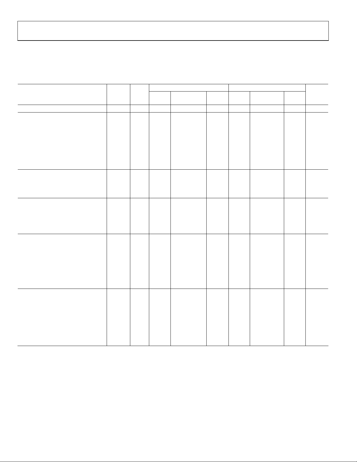
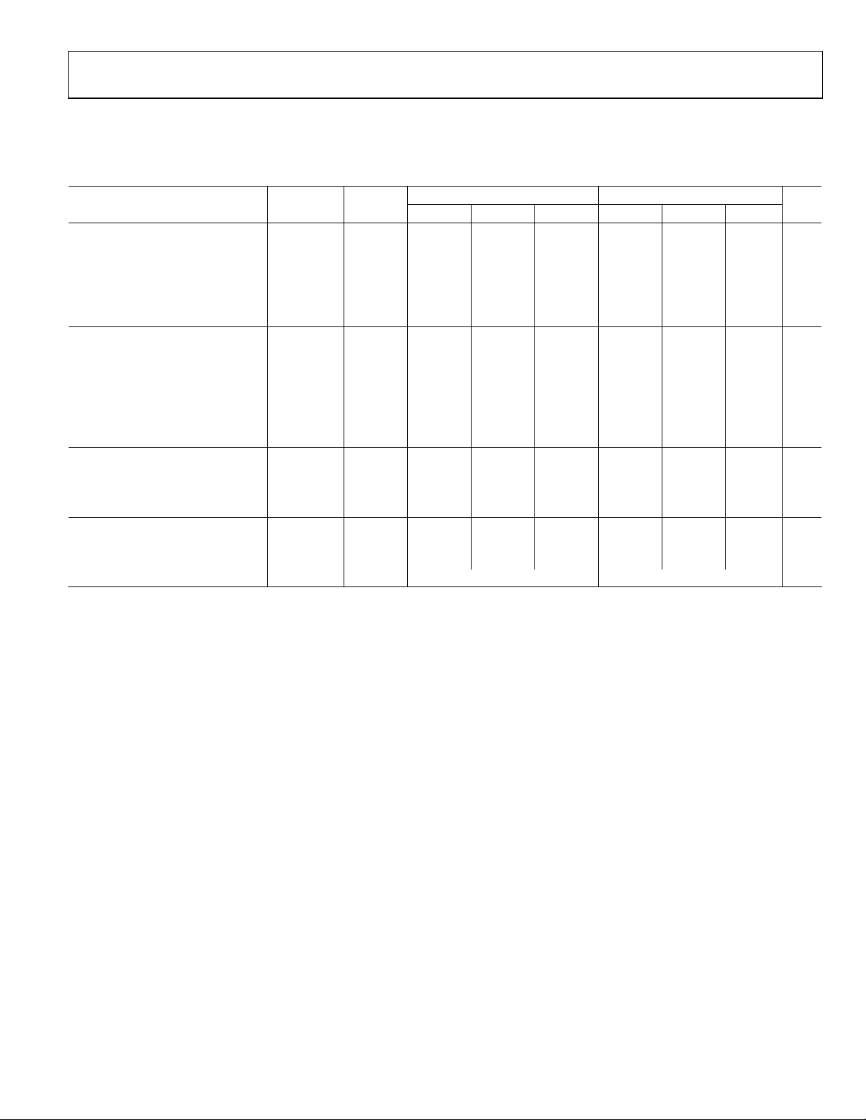
DC SPECIFICATIONS
AVDD = 3.3 V, DRVDD = 3.3 V, T
unless otherwise noted.
Table 1.
AD9430-170 AD9430-210
Parameter
RESOLUTION 12 Bits
ACCURACY
No Missing Codes Full VI Guaranteed Guaranteed
Offset Error 25°C I –3 +3 –3 +3 mV
Gain Error 25°C I –5 +5 –5 +5 % FS
Differential Nonlinearity (DNL) 25°C I –1 ± 0.3 +1 –1 ± 0.3 +1 LSB
Full VI –1 ± 0.3 +1.5 –1 ± 0.3 +1.5 LSB
Integral Nonlinearity (INL) 25°C I –1.5 ± 0.5 +1.5 –1.75 ± 0.3 +1.75 LSB
Full VI –2.25 ± 0.5 +2.25 –2.5 ± 0.3 +2.5 LSB
TEMPERATURE DRIFT
Offset Error Full V 58 58 μV/°C
Gain Error Full V 0.02 0.02 %/°C
Reference Out (VREF) Full V +0.12/–0.24 +0.12/–0.24 mV/°C
REFERENCE
Reference Out (VREF) 25°C I 1.15 1.235 1.3 1.15 1.235 1.3 V
Output Current
I
Input Current2 25°C I 20 20 μA
VREF
I
Input Current
SENSE
1
2
ANALOG INPUTS (VIN+, VIN–)3
Differential Input Voltage Range
(S5 = GND)
Differential Input Voltage Range
(S5 = AVDD)
Input Common-Mode Voltage Full VI 2.65 2.8 2.9 2.65 2.8 2.9 V
Input Resistance Full VI 2.2 3 3.8 2.2 3 3.8 kΩ
Input Capacitance 25°C V 5 5 pF
POWER SUPPLY (LVDS Mode)
AVDD Full IV 3.1 3.3 3.6 3.2 3.3 3.6 V
DRVDD Full IV 3.0 3.3 3.6 3.0 3.3 3.6 V
Supply Currents
I
(AVDD = 3.3 V)
ANALOG
I
(DRVDD = 3.3 V)4 Full VI 55 62 55 62 mA
DIGITAL
4
Power Dissipation4 Full VI 1.29 1.43 1.5 1.7 W
Power Supply Rejection 25°C V –7.5 –7.5 mV/V
= –40°C, T
MIN
Temp
= +85°C, fIN = –0.5 dBFS, internal reference, full scale = 1.536 V, LVDS output mode,
MAX
Te st
Level Min Typ
Max
Min Typ
Max Unit
25°C IV 3.0 3.0 mA
25°C I 1.6 5.0 1.6 5.0 mA
Full V 1.536 1.536 V
Full V 0.766 0.766 V
Full VI 335 372 390 450 mA
Rev. D | Page 4 of 44
Page 5
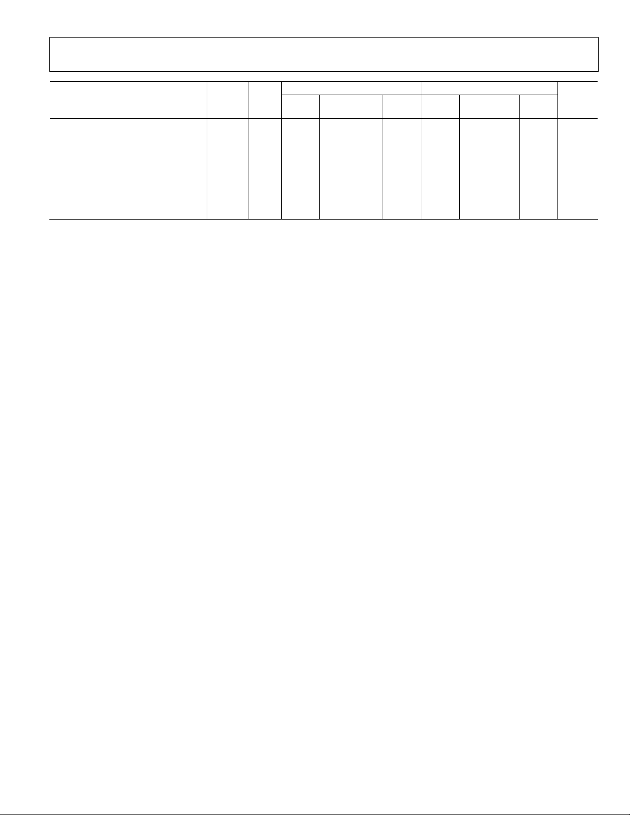
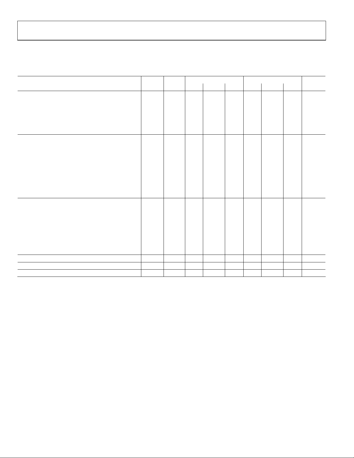
AD9430
AD9430-170 AD9430-210
Parameter
POWER SUPPLY (CMOS Mode)
AVDD Full IV 3.1 3.3 3.6 3.2 3.3 3.6 V
DRVDD Full IV 3.0 3.3 3.6 3.0 3.3 3.6 V
Supply Currents
I
(AVDD = 3.3 V)
AVDD
I
(DRVDD = 3.3 V)5 Full IV 24 30 30 30 mA
DRVDD
Power Dissipation
5
5
Power Supply Rejection 25°C V –7.5 –7.5 mV/V
1
Internal reference mode; SENSE = Floats.
2
External reference mode; SENSE = DRVDD, VREF driven by external 1.23 V reference.
3
S5 (Pin 1) = GND. See the Analog Input section. S5 = GND in all dc and ac tests, unless otherwise noted.
4
I
and I
AVDD
Characteristics and Application Notes sections for I
5
I
AVDD
Characteristics and Application Notes sections for I
are measured with an analog input of 10.3 MHz, –0.5 dBFS, sine wave, rated ENCODE rate, and in LVDS output mode. See Typical Performance
DRVDD
and I
are measured with an analog input of 10.3 MHz, –0.5 dBFS, sine wave, rated ENCODE rate, and in CMOS output mode. See Typical Performance
DRVDD
Temp
Te st
Level Min Typ
Max Min Typ
Max Unit
Full IV 335 372 390 450 mA
Full IV 1.1 1.3 W
. Power consumption is measured with a dc input at rated ENCODE rate in LVDS output mode.
DRVDD
. Power consumption is measured with a dc input at rated ENCODE rate in CMOS output mode.
DRVDD
Rev. D | Page 5 of 44
Page 6
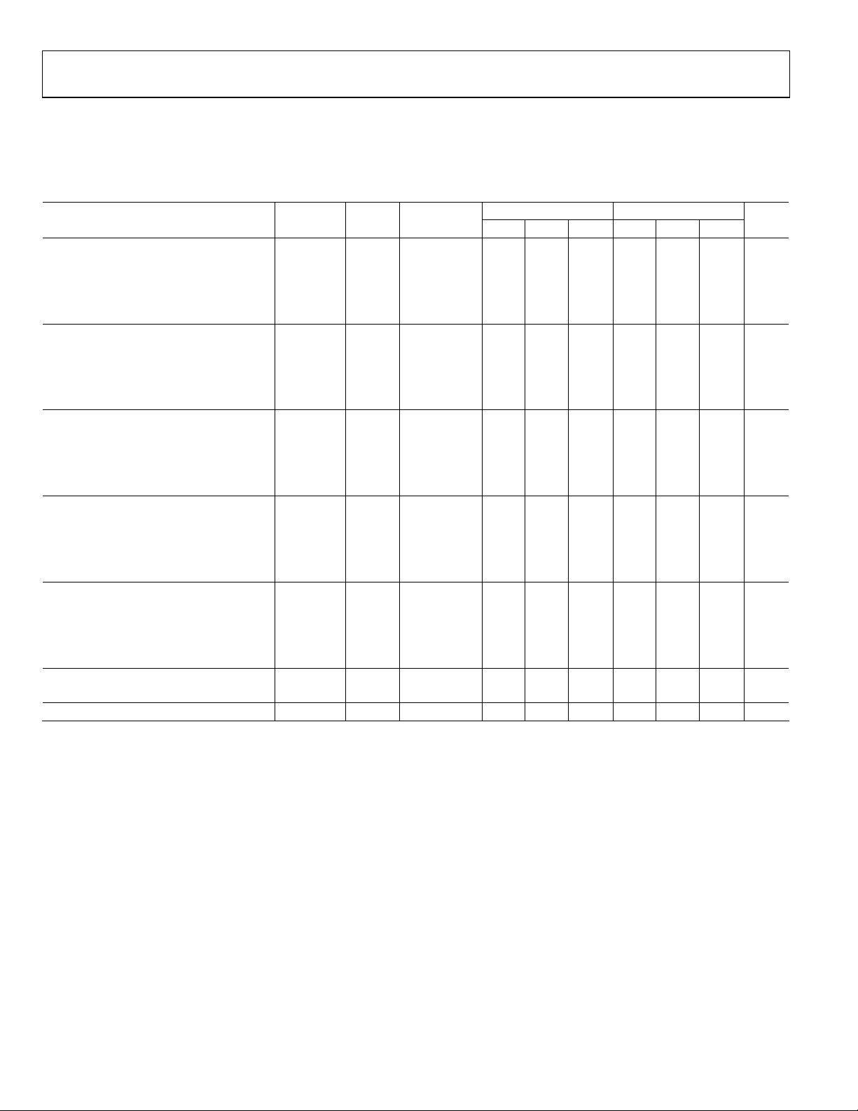
AD9430
AC SPECIFICATIONS
AVDD = 3.3 V, DRVDD = 3.3 V, T
unless otherwise noted.
1
Table 2.
AD9430-170 AD9430-210
Parameter Temp Test Level Min Typ Max Min Typ Max Unit
SNR
Analog Input @ –0.5 dBFS 10 MHz 25°C I 63.5 65 62.5 64.5 dB
70 MHz 25°C I 63 65 62.5 64.5 dB
100 MHz 25°C V 65 64.5 dB
240 MHz 25°C V 61 61 dB
SINAD
Analog Input @ –0.5 dBFS 10 MHz 25°C I 63.5 65 62.5 64.5 dB
70 MHz 25°C I 63 65 62.5 64.5 dB
100 MHz 25°C V 65 64.5 dB
240 MHz 25°C V 60 60 dB
EFFECTIVE NUMBER OF BITS (ENOB)
10 MHz 25°C I 10.3 10.6 10.2 10.5 Bits
70 MHz 25°C I 10.3 10.6 10.2 10.5 Bits
100 MHz 25°C V 10.6 10.5 Bits
240 MHz 25°C V 9.8 9.8 Bits
WORST HARMONIC (2nd or 3rd)
Analog Input @ –0.5 dBFS, 10 MHz 10 MHz 25°C I –85 –75 –84 –74 dBc
70 MHz 25°C I –85 –75 –84 –74 dBc
100 MHz 25°C V –77 –77 dBc
240 MHz 25°C V –63 –63 dBc
WORST HARMONIC (4th or Higher)
Analog Input @ –0.5 dBFS, 10 MHz 10 MHz 25°C I –87 –78 –87 –77 dBc
70 MHz 25°C I –87 –78 –87 –77 dBc
100 MHz 25°C V –77 –77 dBc
240 MHz 25°C V –63 –63 dBc
TWO-TONE IMD
2
F1, F2 @ −7 dBFS 25°C V –75 –75 dBc
ANALOG INPUT BANDWIDTH 25°C V 700 700 MHz
1
All ac specifications tested by differentially driving CLK+ and CLK−.
2
F1 = 28.3 MHz, F2 = 29.3 MHz.
= –40°C, T
MIN
= +85°C, fIN = –0.5 dBFS, internal reference, full scale = 1.536 V, LVDS output mode,
MAX
Rev. D | Page 6 of 44
Page 7
AD9430
DIGITAL SPECIFICATIONS
AVDD = 3.3 V, DRVDD = 3.3 V, T
Table 3.
Test AD9430-170 AD9430-210
Parameter Temp Level Min Typ Max Min Typ Max Unit
ENCODE AND DS INPUTS
(CLK+, CLK–, DS+, DS–)1
Differential Input Voltage2 Full IV 0.2 0.2 V
Common-Mode Voltage3 Full VI 1.375 1.5 1.575 1.375 1.5 1.575 V
Input Resistance Full VI 3.2 5.5 6.5 3.2 5.5 6.5 kΩ
Input Capacitance 25°C V 4 4 pF
LOGIC INPUTS (S1, S2, S4, S5)
Logic 1 Voltage Full IV 2.0 2.0 V
Logic 0 Voltage Full IV 0.8 0.8 V
Logic 1 Input Current Full VI 190 190 μA
Logic 0 Input Current Full VI 10 10 μA
Input Resistance 25°C V 30 30 kΩ
Input Capacitance 25°C V 4 4 pF
LOGIC OUTPUTS (CMOS Mode)
Logic 1 Voltage4 Full IV DRVDD DRVDD V
–0.05 –0.05
Logic 0 Voltage4 Full IV 0.05 0.05 V
LOGIC OUTPUTS (LVDS Mode)
4, 5
VOD Differential Output Voltage Full VI 247 454 247 454 mV
VOS Output Offset Voltage Full VI 1.125 1.375 1.125 1.375 V
Output Coding Twos complement or binary Twos complement or binary
1
ENCODE (Clock) and DS inputs identical on the chip. See the Equivalent Circuits section.
2
All ac specifications tested by driving CLK+ and CLK– differentially, |(CLK+) – (CLK–)| > 200 mV.
3
ENCODE (Clock) inputs’ common-mode can be externally set, such that 0.9 V < (CLK+ or CLK−) < 2.6 V.
4
Digital output logic levels: DRVDD = 3.3 V, C
5
LVDS R
= 100 Ω, LVDS output current set resistor (R
TERM
= –40°C, T
MIN
= +85°C, unless otherwise noted.
MAX
= 5 pF.
LOAD
) = 3.74 kΩ (1% tolerance).
SET
Rev. D | Page 7 of 44
Page 8
AD9430
SWITCHING SPECIFICATIONS
AVDD = 3.3 V, DRVDD = 3.3 V, T
Table 4.
Test AD9430-170 AD9430-210
Parameter (Conditions) Temp Level Min Typ Max Min Typ Max Unit
Maximum Conversion Rate1 Full VI 170
Minimum Conversion Rate
CLK+ Pulse Width High (tEH)
CLK+ Pulse Width Low (tEL)
DS Input Setup Time (t
DS Input Hold Time (t
1
1
Full IV 2
1
Full IV 2
)2 Full IV –0.5 –0.5 ns
SDS
)2 Full IV 1.75 1.75 ns
HDS
OUTPUT (CMOS Mode)
Valid Time (tV) Full IV 2 2 ns
Propagation Delay (tPD) Full IV 3.8 5 3.8 5 ns
Rise Time (tR) (20% to 80%) 25°C V 1 1 ns
Fall Time (tF) (20% to 80%) 25°C V 1 1 ns
DCO Propagation Delay (t
Data to DCO Skew (tPD to t
CPD
CPD
Interleaved Mode (A, B Latency) Full IV 14, 14 14, 14 Cycles
Parallel Mode (A, B Latency) Full IV 15, 14 15, 14 Cycles
OUTPUT (LVDS Mode)
Valid Time (tV) Full VI 2.0 2.0 ns
Propagation Delay (tPD) Full VI 3.2 4.3 3.2 4.3 ns
Rise Time (tR) (20% to 80%) 25°C V 0.5 0.5 ns
Fall Time (tF) (20% to 80%) 25°C V 0.5 0.5 ns
DCO Propagation Delay (t
Data to DCO Skew (tPD – t
CPD
CPD
Latency Full IV 14 14 Cycles
APERTURE DELAY (tA) 25°C V 1.2 1.2 ns
APERTURE UNCERTAINTY (Jitter, tJ) 25°C V 0.25 0.25 ps rms
OUT OF RANGE RECOVERY TIME (CMOS and LVDS) 25°C V 1 1 Cycles
1
All ac specifications tested by differentially driving CLK+ and CLK−.
2
DS inputs used in CMOS mode only.
= –40°C, T
MIN
= +85°C, unless otherwise noted.
MAX
Full V
40
12.5 2
12.5 2
210
MSPS
40 MSPS
12.5 ns
12.5 ns
) Full IV 3.8 5 3.8 5 ns
) Full IV –0.5 0 +0.5 –0.5 0 +0.5 ns
) Full VI 1.8 2.7 3.8 1.8 2.7 3.8 ns
) Full IV 0.2 0.5 0.8 0.2 0.5 0.8 ns
Rev. D | Page 8 of 44
Page 9
AD9430
–
TIMING DIAGRAMS
CLK+
CLK–
DS+
DS–
PORT A
DA11–DA0
PORT B
DB11–DB0
PORT A
DA11–DA0
PORT B
DB11–DB0
DCO–
DCO+
t
HDS
INTERLEAVED DATA OUT
STATIC
STATIC
PARALLEL DATA OUT
STATIC
STATIC
STATIC
t
SDS
14 CYCLES
INVALID
INVALID
INVALID
INVALID
Figure 2. CMOS Timing Diagram
INVALID
INVALID
INVALID
t
PD
N N+2
N+1
N N+2
N+1 N+3
t
CPD
N+3
t
V
02607-002
1
N
A
IN
N
N+1
t
EL
t
EH
CLK+
CLK–
DATA OUT
DCO+
DCO–
t
CPD
1/f
S
t
PD
N–14
N–13
14 CYCLES
Figure 3. LVDS Timing Diagram
N
N+1
02607-003
Rev. D | Page 9 of 44
Page 10
AD9430
ABSOLUTE MAXIMUM RATINGS
Table 5.
Parameter Rating
AVDD, DRVDD 4 V
Analog Inputs –0.5 V to AVDD + 0.5 V
Digital Inputs –0.5 V to DRVDD + 0.5 V
REFIN Inputs –0.5 V to AVDD + 0.5 V
Digital Output Current 20 mA
Operating Temperature –55°C to +125°C
Storage Temperature –65°C to +150°C
Maximum Junction Temperature 150°C
Maximum Case Temperature 150°C
1
θ
JA
1
Typical θJA = 32°C/W (heat slug not soldered); typical θJA = 25°C/W (heat slug
soldered) for multilayer board in still air with solid ground plane.
25°C/W, 32°C/W
Stresses above those listed under Absolute Maximum Ratings
may cause permanent damage to the device. This is a stress
rating only; functional operation of the device at these or any
other conditions above those listed in the operational section
of this specification is not implied. Exposure to absolute
maximum rating conditions for extended periods may affect
device reliability.
EXPLANATION OF TEST LEVELS
Table 6.
Level Description
I 100% production tested.
II
III Sample tested only.
IV
V Parameter is a typical value only.
VI
100% production tested at 25°C and sample tested at
specified temperatures.
Parameter is guaranteed by design and
characterization testing.
100% production tested at 25°C; guaranteed by
design and characterization testing for industrial
temperature range; 100% production tested at
temperature extremes for military devices.
ESD CAUTION
ESD (electrostatic discharge) sensitive device. Electrostatic charges as high as 4000 V readily accumulate on the
human body and test equipment and can discharge without detection. Although this product features
proprietary ESD protection circuitry, permanent damage may occur on devices subjected to high energy
electrostatic discharges. Therefore, proper ESD precautions are recommended to avoid performance
degradation or loss of functionality.
Rev. D | Page 10 of 44
Page 11
AD9430
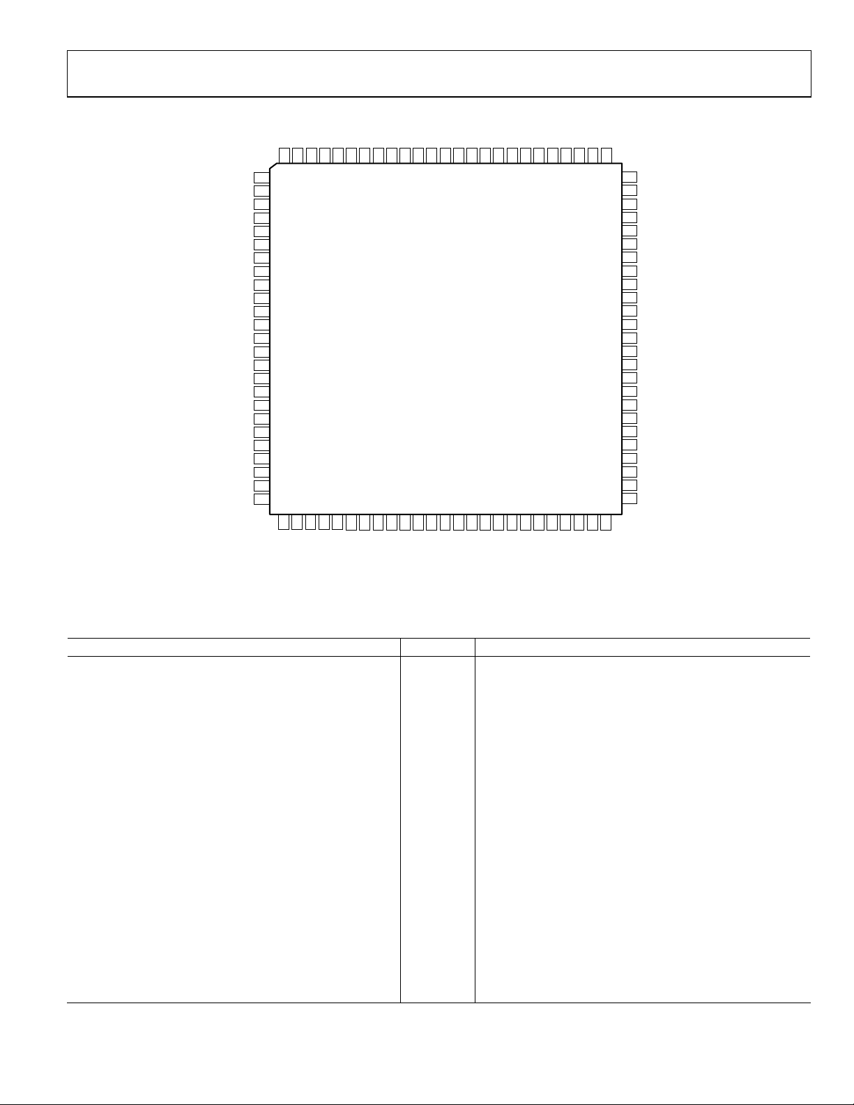
PIN CONFIGURATIONS AND FUNCTION DESCRIPTIONS
DRVDD
DRGND
DA10
81
82
4445464748
DB1
DB0
DNC
DA979DA878DA777DA676DA5
80
50
49
DB2
DB3
DB4
DRVDD
DRGND
75
74
73
72
71
70
69
68
67
66
65
64
63
62
61
60
59
58
57
56
55
54
53
52
51
DRVDD
DRGND
DA4
DA3
DA2
DA1
DA0
DNC
DRGND
DNC
DNC
DCO+
DCO–
DRVDD
DRGND
OR_B
DB11
DB10
DB9
DB8
DB7
DRVDD
DRGND
DB6
DB5
02607-004
DNC
AGND
DNC
AVDD
AGND
SENSE
VREF
AGND
AGND
AVDD
AVDD
AGND
AGND
AVDD
AVDD
AGND
VIN+
VIN–
AGND
AVDD
AGND
AGND
AVDD
AVDD
AGND
AGND
AVDD
AVDD
AGND
AGND
AGND
AVDD
AVDD
AVDD
AGND
AGND
OR_A
DA11
99989796959493
100
S5
1
2
S4
3
4
S2
5
S1
6
7
8
9
10
11
12
13
14
15
16
17
18
19
20
21
22
23
24
25
2627282930
AVDD
AVDD
AVDD
AGND
AGND
31
AGND
929190
89
88
8786858483
AD9430
CMOS PI NO UT
TOP VIEW
(Not to S cale)
33
32
343536
DS+
DS–
AVDD
AGND
CLK+
39
37
40
38
414243
AVDD
AVDD
DNC
AGND
CLK–
AGND
Figure 4. CMOS Dual-Mode Pin Configuration
Table 7. CMOS Mode Pin Function Descriptions
Pin Number Mnemonic Description
1 S5
Full-Scale Adjust Pin. AVDD sets f
GND sets f
= 1.536 V p-p differential.
S
= 0.768 V p-p differential,
S
2, 7, 42, 43, 65, 66, 68 DNC Do Not Connect.
3 S4 Interleaved, Parallel Select Pin. High = interleaved.
1
Analog Ground.
4, 9, 12, 13, 16, 17, 20, 23, 25, 26, 30, 31, 35, 38, 41, 86,
AGND
87, 91, 92, 93, 96, 97, 100
5 S2 Output Mode Select. Low = dual-port CMOS, high = LVDS.
6 S1
Data Format Select. Low = binary, high = twos complement for
both CMOS and LVDS modes.
8, 14, 15, 18, 19, 24, 27, 28, 29, 34, 39, 40, 88, 89, 90, 94,
AVDD 3.3 V Analog Supply.
95, 98, 99
10 SENSE Reference Mode Select Pin. Float for internal reference operation.
11 VREF 1.235 V Reference I/O—Function Dependent on SENSE.
21 VIN+ Analog Input—True.
22 VIN– Analog Input—Complement.
32 DS+ Data Sync (Input)—True. Tie low if not used.
33 DS–2 Data Sync (Input)—Complement. Tie high if not used.
36 CLK+ Clock Input—True.
37 CLK– Clock Input—Complement.
44 DB0 B Port Output Data Bit (LSB).
45 DB1 B Port Output Data Bit.
Rev. D | Page 11 of 44
Page 12

AD9430
Pin Number Mnemonic Description
46 DB2 B Port Output Data Bit.
47, 54, 62, 75, 83 DRVDD 3.3 V Digital Output Supply (3.0 V to 3.6 V).
48, 53, 61, 67, 74, 82 DRGND1 Digital Output Ground.
49 DB3 B Port Output Data Bit.
50 DB4 B Port Output Data Bit.
51 DB5 B Port Output Data Bit.
52 DB6 B Port Output Data Bit.
55 DB7 B Port Output Data Bit.
56 DB8 B Port Output Data Bit.
57 DB9 B Port Output Data Bit.
58 DB10 B Port Output Data Bit.
59 DB11 B Port Output Data Bit (MSB).
60 OR_B B Port Overrange.
63 DCO– Data Clock Output—Complement.
64 DCO+ Data Clock Output—True.
69 DA0 A Port Output Data Bit (LSB).
70 DA1 A Port Output Data Bit.
71 DA2 A Port Output Data Bit.
72 DA3 A Port Output Data Bit.
73 DA4 A Port Output Data Bit.
76 DA5 A Port Output Data Bit.
77 DA6 A Port Output Data Bit.
78 DA7 A Port Output Data Bit.
79 DA8 A Port Output Data Bit.
80 DA9 A Port Output Data Bit.
81 DA10 A Port Output Data Bit.
84 DA11 A Port Output Data Bit (MSB).
85 OR_A A Port Overrange.
1
AGND and DRGND should be tied together to a common ground plane.
2
DS Complement (DS−); can be tied to AVDD (as recommended) or left floating with no ill effects.
Rev. D | Page 12 of 44
Page 13
AD9430
AGND
AVDD
AVDD
AGND
AGND
AVDD
AVDD
AGND
AGND
AGND
AVDD
AVDD
AVDD
AGND
AGND
OR+
OR–
DRVDD
DRGND
D11+
D11–79D10+78D10–77D9+76D9–
DNC
DNC
81
82
80
4445464748
DNC
DNC
DNC
DRVDD
49
D0–
DRGND
75
DRVDD
74
DRGND
73
D8+
72
D8–
71
D7+
70
D7–
69
D6+
68
D6–
67
DRGND
66
D5+
65
D5–
64
DCO+
63
DCO–
62
DRVDD
61
DRGND
60
D4+
59
D4–
58
D3+
57
D3–
56
D2+
D2–
55
54
DRVDD
53
DRGND
52
D1+
51
D1–
50
D0+
02607-005
DNC
AGND
LVDSBIAS
AVDD
AGND
SENSE
VREF
AGND
AGND
AVDD
AVDD
AGND
AGND
AVDD
AVDD
AGND
VIN+
VIN–
AGND
AVDD
AGND
99989796959493
100
S5
1
2
3
S4
4
5
S2
S1
6
7
8
9
10
11
12
13
14
15
16
17
18
19
20
21
22
23
24
25
2627282930
AVDD
AVDD
AVDD
AGND
AGND
31
32
GND
AGND
929190
33
343536
AVDD
AVDD
89
AD9430
LVDS PINOUT
TOP VIEW
(Not to Scale)
37
CLK–
CLK+
AGND
8786858483
88
39
40
38
AVDD
AVDD
AGND
414243
AGND
Figure 5. LVDS Mode Pin Configuration
Table 8. LVDS Mode Pin Function Descriptions
Pin Number Mnemonic Description
1 S5 Full-Scale Adjust Pin. AVDD sets fS = 0.768 V p-p differential,
GND sets fS = 1.536 V p-p differential.
2, 42 to 46 DNC Do Not Connect.
3 S4
Control Pin for CMOS Mode. Tie low when operating in LVDS
mode.
1
Analog Ground.
4, 9, 12, 13, 16, 17, 20, 23, 25, 26, 30, 31, 35, 38, 41, 86, 87, 91,
AGND
92, 93, 96, 97, 100
5 S2 Output Mode Select. GND = dual-port CMOS; AVDD = LVDS.
6 S1
7 LVDSBIAS
Data Format Select. GND = binary, AVDD = twos complement.
Set Pin for LVDS Output Current. Place 3.74 kW resistor
terminated to ground.
8, 14, 15, 18, 19, 24, 27, 28, 29, 33, 34, 39, 40, 88, 89, 90, 94, 95,
98, 99
10 SENSE
AVD D2 3.3 V Analog Supply.
Reference Mode Select Pin. Float for internal reference
operation.
11 VREF 1.235 V Reference I/O—Function Dependent on SENSE.
21 VIN+ Analog Input—True.
22 VIN– Analog Input—Complement.
32 GND Data Sync (Input)—Not Used in LVDS Mode. Tie to GND.
36 CLK+ Clock Input—True (LVPECL Levels).
37 CLK– Clock Input—Complement (LVPECL Levels).
Rev. D | Page 13 of 44
Page 14

AD9430
Pin Number Mnemonic Description
47, 54, 62, 75, 83 DRVDD 3.3 V Digital Output Supply (3.0 V to 3.6 V).
48, 53, 61, 67, 74, 82 DRGND1 Digital Output Ground.
49 D0– D0 Complement Output Bit (LSB).
50 D0+ D0 True Output Bit (LSB).
51 D1– D1 Complement Output Bit.
52 D1+ D1 True Output Bit.
55 D2– D2 Complement Output Bit.
56 D2+ D2 True Output Bit.
57 D3– D3 Complement Output Bit.
58 D3+ D3 True Output Bit.
59 D4– D4 Complement Output Bit.
60 D4+ D4 True Output Bit.
63 DCO– Data Clock Output—Complement.
64 DCO+ Data Clock Output—True.
65 D5– D5 Complement Output Bit.
66 D5+ D5 True Output Bit.
68 D6– D6 Complement Output Bit.
69 D6+ D6 True Output Bit.
70 D7– D7 Complement Output Bit.
71 D7+ D7 True Output Bit.
72 D8– D8 Complement Output Bit.
73 D8+ D8 True Output Bit.
76 D9– D9 Complement Output Bit.
77 D9+ D9 True Output Bit.
78 D10– D10 Complement Output Bit.
79 D10+ D10 True Output Bit.
80 D11– D11 Complement Output Bit.
81 D11+ D11 True Output Bit.
84 OR– Overrange Complement Output Bit.
85 OR+ Overrange True Output Bit.
1
AGND and DRGND should be tied together to a common ground plane.
2
Pin 33 can be tied to AVDD (as recommended) or left floating with no ill effects
Rev. D | Page 14 of 44
Page 15

AD9430
V
EQUIVALENT CIRCUITS
FULL
K
SCALE
S5 = 0 —> K = 1.24
S5 = 1 —> K = 0.62
A1
Ω
200
1k
Ω
VDD
Figure 9. VREF, SENSE I/O
DR
DD
VREF
0.1μF
SENSE
02607-009
CLK+
OR
DS+
AVDD
12kΩ
150Ω 150Ω
10kΩ
Figure 6. ENCODE and DS Input
3.5k
Ω
3.5k
12kΩ
10kΩ
CLK–
OR
DS–
02607-080
+
–
1V
DISABLE
A1
AVDD
Ω
VIN+
S1, S2,
S4, S5
20k
Ω
Figure 7. Analog Inputs
Figure 8. S1 to S5 Inputs
30k
VIN–
20k
Ω
02607-007
VDD
Ω
02607-008
Figure 10. Data Outputs (CMOS Mode)
V
DX–
V
DX
02607-010
DRVDD
V
DX+
V
02607-011
Figure 11. Data Outputs (LVDS Mode)
Rev. D | Page 15 of 44
Page 16

AD9430
TYPICAL PERFORMANCE CHARACTERISTICS
Charts at 170 MSPS, 210 MSPS for –170, –210 grades, respectively. AVDD, DRVDD = 3.3 V, T = 25°C, AIN differential drive, full
scale = 1.536 V, internal reference unless otherwise noted.
0
–10
–20
–30
–40
–50
dB
–60
–70
–80
–90
–100
04010 20 30 50 60 70 80
Figure 12. FFT: f
0
–10
–20
–30
–40
–50
dB
–60
–70
–80
–90
–100
04010 20 30 50 60 70 80
Figure 13. FFT: f
SNR = 65.2dB
SINAD = 65.1dB
H2 = –88.8dBc
H3 = –88.1dBc
SFDR = 87dBc
MHz
= 170 MSPS, AIN = 10.3 MHz @ −0.5 dBFS, LVDS Mode
s
SNR = 65.1dB
SINAD = 64.9dB
FUND = –0.50dBFS
H2 = –88.6dBc
H3 = –94.6dBc
SFDR = 85.9dBc
MHz
= 170 MSPS, AIN = 65 MHz @ –0.5 dBFS, LVDS Mode
s
85
02607-012
85
02607-013
0
–10
–20
–30
–40
dB
–50
–60
–70
–80
–90
–100
04010 20 30 50 60 70 80
Figure 15. FFT: f
SNR = 62.99dBFS
SINAD = 61.45dBFS
H2 = –66.8dBc
H3 = –82.5dBc
SFDR = 66.1dBc
MHz
= 170 MSPS, AIN = 10.3 MHz @ –0.5 dBFS,
s
Single-Ended Input, Full Scale = 0.76 V, LVDS Mode
0
–10
–20
–30
–40
–50
dB
–60
–70
–80
–90
–100
0 153045 607590105
Figure 16. FFT: f
= 210 MSPS, AIN = 10.3 MHZ @ –0.5 dBFS, LVDS Mode
s
MHz
SNR = 63.6dB
SINAD = 62.9dB
H2 = –82.5dBc
H3 = –78.6dBc
SFDR = 77.7dBc
85
02607-015
02607-016
0
SNR = 64.93dB
–10
SINAD = 64.85dB
FUND = –0.44dBFS
–20
H2 = –92.1dBc
H3 = –90.1dBc
SFDR = 75.6dBc
–30
–40
–50
dB
–60
–70
–80
–90
–100
04010 20 30 50 60 70 80
Figure 14. FFT: f
= 170 MSPS, AIN = 65 MHz @ –0.5 dBFS, CMOS Mode
s
MHz
85
02607-015
Figure 17. FFT: f
Rev. D | Page 16 of 44
0
–10
–20
–30
–40
–50
dB
–60
–70
–80
–90
–100
0 15 30 45 60 75 90 105
= 210 MSPS, AIN = 65 MHz @ –0.5 dBFS, CMOS Mode
s
MHz
SNR = 63.1dB
SINAD = 62.8dB
H2 = –81.1dBc
H3 = –76dBc
SFDR = –76dBc
02607-017
Page 17

AD9430
0
–10
–20
–30
–40
–50
dB
–60
–70
–80
–90
–100
0 15 30 45 60 75 90 105
Figure 18. FFT: f
= 210 MSPS, AIN = 65 MHz @ –0.5 dBFS, LVDS Mode
s
MHz
SNR = 63.5dB
SINAD = 62.6dB
H2 = –79dBc
H3 = –76.1dBc
SFDR = 75.2dBc
02607-018
0
SNR = 63.3dB
–10
SINAD = 63.1dB
H2 = –80.38dBc
–20
H3 = –81.8dBc
SFDR = 80.8dBc
–30
–40
–50
dB
–60
–70
–80
–90
–100
0 153045607590105
Figure 21. FFT: f
= 213 MSP, AIN = 100 MHz @ –0.5 dBFS, LVDS Mode
s
MHz
02607-021
85
80
75
70
65
dB
60
55
FULL SCALE = 1.5
50
45
40
0 100 150 250 35050 200 300 400
Figure 19. SNR, SINAD, and SFDR vs. A
100
THIRD
90
80
SFDR
70
dB
SFDR
SNR
AIN (MHz)
@ –0.5 dBFS, LVDS Mode
A
IN
IN
Frequency, fS = 210 MSPS,
SECOND
SINAD
02607-019
85
80
75
70
65
dB
60
55
FULL SCALE = 0.75
50
45
40
0 100 150 250 35050 200 300 400
Figure 22. SNR and SINAD vs. A
@ –0.5 dBFS, LVDS Mode, Full Scale = 0.76 V
A
IN
100
90
THIRD
80
SFDR
70
dB
SNR
SINAD
AIN (MHz)
Frequency, fs = 210 MSPS,
IN
SECOND
02607-022
60
50
40
0 200 40050 100 150 250 300 350
Figure 20. Harmonic Distortion (2
AIN(MHz)
and SFDR vs. A
Frequency
IN
nd
and 3rd)
02607-020
Rev. D | Page 17 of 44
60
50
40
0 200 40050 100 150 250 300 350
Figure 23. Harmonic Distortion (2
SFDR vs. A
Frequency, fs = 170 MSPS, CMOS Mode
IN
AIN(MHz)
nd
and 3rd) and
02607-023
Page 18

AD9430
70
68
66
64
62
60
dB
58
56
54
52
50
0 100 15050 200 250 300 350 400
Figure 24. SNR and SINAD vs. A
85
80
75
70
65
dB
60
55
50
45
40
0 100 150 250 35050 200 300 400
Figure 25. SNR and SINAD, SFDR vs. A
f
= 210 MSPS, AIN @ –0.5 dBFS, CMOS Mode
s
0
SFDR = 75dBc
–10
–20
–30
–40
dB
–50
–60
–70
–80
–90
–100
04010 20 30 50 60 70 80
Figure 26. Two-Tone Intermodulation Distortion
(28.3 MHz and 29.3 MHz, LVDS Mode, f
–170 SINAD
AIN (MHz)
Frequency, fs = 170 MSPS/210 MSPS,
IN
@ –0.5 dBFS, LVDS Mode
A
IN
SFDR
SNR
AIN (MHz)
MHz
–170 SNR
IN
–210 SNR
–210 SINAD
SINAD
Frequency,
= 170 MSPS)
s
02607-024
02607-025
85
02607-026
0
–30
–60
dB
–90
–120
0 102030405060 809010070
SFDR = 63dBc
MHz
Figure 27. Two-Tone Intermodulation Distortion (59 MHz and 60 MHz),
LVDS Mode, f
95
90
85
80
75
dB
70
65
60
55
50
0 25050 100 150 200
= 210 MSPS
s
SFDR
SINAD
MHz
02607-028
Figure 28. SINAD and SFDR vs. Clock Rate
= 10.3 MHz @ –0.5 dBFS, LVDS Mode), –170 Grade
(A
IN
85
80
75
70
65
dB
60
55
50
45
40
0 100 150 25050 200
SINAD
SNR
SFDR
MHz
02607-029
Figure 29. SNR and SINAD, SFDR vs. Clock Rate
= 10.3 MHz, @ –0.5 dBFS), LVDS Mode, –210 Grade
(A
IN
02607-027
Rev. D | Page 18 of 44
Page 19

AD9430
400
ANALOG SUPPLY
CURRENT CMOS
350
MODE
300
250
OUTPUT SUPPLY
CURRENT LVDS
200
MODE
150
100
(ANALOG SUPPLY CURRENT) (mA)
50
AVDD
I
0
100 220140 160 180 200120
Figure 30. I
AVDD
and I
ANALOG SUPPLY
CURRENT LVDS
MODE
ENCODE (MSPS)
vs. Clock Rate (AIN = 10.3 MHz @ –0.5 dBFS)
DRVDD
170 MSPS Grade, C
450
ANALOG SUPPLY
400
CURRENT LVDS MODE
350
300
250
200
150
100
(ANALOG SUPPLY CURRENT) (mA)
50
AVDD
I
0
100 140 160 200
(A
85
OUTPUT SUPPLY
CURRENT LVDS MODE
OUTPUT SUPPLY
CURRENT CMOS MODE
120 180
Figure 31. I
= 10.3 MHz @ –0.5 dBFS), 210 MSPS Grade, C
IN
ENCODE (MSPS)
and I
AVDD
OUTPUT SUPPLY
CURRENT CMOS
MODE
= 5 pF
LOAD
ANALOG SUPPLY
CURRENT CMOS MODE
vs. Clock Rate
DRVDD
220
LOAD
240
= 5 pF
80
60
40
20
(OUTPUT SUPPLY CURRE NT) (mA)
DRVDD
I
0
02607-030
90
80
70
60
50
40
30
20
(OUTPUT SUPPLY CURRENT) (mA)
10
DRVDD
I
0
02607-031
80
75
70
65
dB
60
55
50
20 40 50 7030 60 80
ENCODE POSITIVE DUTY CYCLE (%)
SFDR
SNR
SINAD
Figure 33. SNR, SINAD, and SFDR vs. ENCODE Pulse Width High,
= 10.3 MHz @ –0.5 dBFS, 210 MSPS, LVDS)
(A
IN
1.4
1.2
1.0
0.8
(V)
0.6
REFOUT
V
0.4
0.2
0
081472
2.0
RO = 13Ω TYP
Figure 34. V
I
LOAD
536
(mA)
vs. I
REFOUT
LOAD
02607-033
02607-034
80
75
70
dB
65
60
55
50
10 60 9020 40 50 70 8030
SFDR
SNR
SINAD
ENCODE POSITIVE DUTY CYCLE (%)
Figure 32. SINAD and SFDR vs. Clock Pulse Width High
(A
= 10.3 MHz @ –0.5 dBFS, 170 MSPS, LVDS)
IN
02607-032
Rev. D | Page 19 of 44
1.5
1.0
0.5
0
–0.5
GAIN ERROR (%)
–1.0
–1.5
–2.0
–50 10 95–30 –10 30 50 70 90
TEMPERATURE (°C)
% GAIN ERROR
USING EXT REF
Figure 35. Full-Scale Gain Error vs. Temperature
(A
= 10.3 MHz @ –0.5 dBFS, 170 MSPS/210 MSPS, LVDS)
IN
02607-035
Page 20

AD9430
1.250
1.245
1.00
0.75
0.50
1.240
(V)
REF
V
1.235
1.230
1.225
2.5 3.12.7 2.9 3.3 3.5 3.7 3.9
Figure 36. V
95
90
85
80
dB
75
70
65
60
–50 10–30 –10 30 50 70 90
SFDR
AVDD (V)
Output Voltage vs. AVDD
REF
THIRD
SECOND
TEMPERATURE (°C)
Figure 37. SNR, SINAD, and SFDR vs. Temperature
= 10.3 MHz @ –0.5 dBFS, 170 MSPS)
(A
IN
65
64
63
62
61
60
dB
59
58
57
56
55
–45 –5 15 55–25 35 75
TEMPERATURE (°C)
AVDD = 3.135
AVDD = 3.0
Figure 38. SINAD vs. Temperature, AVDD
(A
= 70 MHz @ –0.5 dB, 210 MSPS, LVDS Mode)
IN
SNR
SINAD
AVDD = 3.6
AVDD = 3.3
02607-036
02607-037
02607-038
0.25
0
LSB
–0.25
–0.50
–0.75
–1.00
0 4000500 1500 2500 30001000 2000 3500
Figure 39. Typical INL Plot (A
1.00
0.75
0.50
0.25
0
LSB
–0.25
–0.50
–0.75
–1.00
0 4000500 1500 2500 30001000 2000 3500
Figure 40. Typical DNL Plot (A
100
90
80
70
60
50
dB
40
30
20
10
0
–100 0–70 –50 –30 –20–60 –40 –10–80–90
SFDR –dBFS
SFDR –dBc
ANALOG INPUT LEVEL (dBFS)
Figure 41. SFDR vs. A
@ 10.3 MHz, 170 MSPS, LVDS Mode
A
IN
CODE
= 10.3 MHz @ –0.5 dBFS, 170 MSPS, LVDS)
IN
CODE
= 10.3 MHz @ –0.5 dBFS)
IN
Input Level ,
IN
80dB
REFERENCE LINE
02607-039
02607-040
02607-041
Rev. D | Page 20 of 44
Page 21

AD9430
90
80
70
60
50
dB
40
30
20
10
0
–90 –70 –60 –40 –20–80 –50 –30 –10
Figure 42. SFDR vs. A
SFDR dBc
LVDS MODE
FULL SCALE = 1.5
80dB REFERENCE LINE
Input Level, AIN @ 10.3 MHz, 210 MSPS,
IN
LVDS/CMOS Modes
90
80
70
60
50
dB
40
30
20
10
0
–90 –70 –60 –40 –20–80 –50 –30 –10
Figure 43. SFDR vs. A
SFDR dBc
LVDS MODE
FULL SCALE = 1.5
80dB REFERENCE LINE
Input Level, AIN @ 10.3 MHz, 210 MSPS, LVDS Mode,
IN
Full Scale = 0.76 V/1.536 V
0
NPR = 56.95dB
ENCODE = 170MSPS
–20
NOTCH @ 19MHz
–40
SFDR dBc
CMOS MODE
FULL SCALE = 1.5
SFDR dBc
LVDS MODE
FULL SCALE = 0.75
0
0
02607-042
02607-043
0
–20
–40
dB
–60
–80
–100
19.2 38.4
19.2
MHz
Figure 45. W-CDMA Four Channels Centered at 38.4 MHz,
= 153.6 MHz, LVDS Mode
f
s
90
80
70
60
50
dB
40
30
20
10
0
0 2.52.01.0 1.50.5
FULL-SCALE RANGE (V)
SFDR
SNR
SINAD
Figure 46. SNR, SINAD, and SFDR vs. Full-Scale Range, S5 = 0,
Full-Scale Range Varied by Adjusting VREF, 170 MSPS
4.5
4.0
47.6
02607-045
02607-046
–60
–80
–100
NOISE INPUT LEVEL (dB)
–120
–140
2.65 42.521.25
Figure 44. Noise Power Ratio Plot
MHz
02607-044
Rev. D | Page 21 of 44
3.5
ns
TPD
3.0
TCPD
2.5
–40 1006020 40–20 0 80
TEMPERATURE (°C)
Figure 47. Propagation Delay vs. Temperature, LVDS Mode,
170 MSPS/210 MSPS
02607-047
Page 22

AD9430
4.5
4.0
3.5
ns
3.0
2.5
–40 1006020 40–20 0 80
TCPD (CLOCKOUT RISING)
TPDF (DATA FALLING)
TPDR (DATA RISING)
TEMPERATURE (°C)
Figure 48. Propagation Delay vs. Temperature,
CMOS Mode, 170 MSPS/210 MSPS
02607-048
900
800
700
600
500
(mV)
DIF
400
V
300
200
100
0
0110621
V
OS
V
OD
84
RSET (kΩ)
1.4
1.3
1.2
1.1
1.0
(V)
OS
0.9
V
0.8
0.7
0.6
0.5
42
02607-049
Figure 49. LVDS Output Swing, Common-Mode Voltage vs. RSET,
Placed at LVDSBIAS, 170 MSPS/210 MSPS
Rev. D | Page 22 of 44
Page 23

AD9430
TERMINOLOGY
Analog Bandwidth
The analog input frequency at which the spectral power of the
fundamental frequency (as determined by the FFT analysis) is
reduced by 3 dB.
Aperture Delay
The delay between the 50% point of the rising edge of the
ENCODE command and the instant at which the analog input
is sampled.
Aperture Uncertainty (Jitter)
The sample-to-sample variation in aperture delay.
Crosstalk
Coupling onto one channel being driven by a low level
(–40 dBFS) signal when the adjacent interfering channel is
driven by a full-scale signal.
Differential Analog Input Resistance, Differential Analog
Input Capacitance, and Differential Analog Input Impedance
The real and complex impedances measured at each analog
input port. The resistance is measured statically and the
capacitance and differential input impedances are measured
with a network analyzer.
Differential Analog Input Voltage Range
The peak-to-peak differential voltage that must be applied to
the converter to generate a full-scale response. Peak differential
voltage is computed by observing the voltage on a single pin
and subtracting the voltage from the other pin, which is
180° out of phase. Peak-to-peak differential is computed by
rotating the input phase 180° and again taking the peak
measurement. The difference is then computed between both
peak measurements.
Differential Nonlinearity
The deviation of any code width from an ideal 1 LSB step.
Effective Number of Bits (ENOB)
Calculated from the measured SNR based on the equation
ENOB
SNR
MEASURED
=
6.02
dB1.76−
ENCODE Pulse Width/Duty Cycle
Pulse width high is the minimum amount of time the ENCODE
pulse (clock pulse) should be left in a Logic 1 state to achieve
rated performance; pulse width low is the minimum time the
ENCODE pulse should be left in a low state. See the timing
implications of changing t
in the Encode Input section. At
EH
a given clock rate, these specifications define an acceptable
ENCODE duty cycle.
Full-Scale Input Power
Expressed in dBm. Computed using the following equation:
Power
⎛
2
⎜
V
⎜
=
SCALEFULL
log10
Z
⎜
INPUT
⎜
001.0
⎝
⎞
⎟
rmsSCALEFULL
⎟
⎟
⎟
⎠
Gain Error
The difference between the measured and ideal full-scale input
voltage range of the ADC.
Harmonic Distortion, Second
The ratio of the rms signal amplitude to the rms value of the
second harmonic component, reported in dBc.
Harmonic Distortion, Third
The ratio of the rms signal amplitude to the rms value of the
third harmonic component, reported in dBc.
Integral Nonlinearity
The deviation of the transfer function from a reference line
measured in fractions of 1 LSB using a best straight line
determined by a least square curve fit.
Minimum Conversion Rate
The ENCODE rate at which the SNR of the lowest analog
signal
frequency drops by no more than 3 dB below the
guaranteed limit.
Maximum Conversion Rate
The ENCODE rate at which parametric testing is performed.
Output Propagation Delay
The delay between a differential crossing of CLK+ and CLK– and
the time when all output data bits are within valid logic levels.
Noise (for Any Range Within the ADC)
Calculated as follows:
NOISE
⎛
××=
ZV
10001.0
⎜
⎝
SignalSNRFS
10
⎞
dBFSdBcdBM
⎟
⎠
−−
where:
Z is the input impedance.
FS is the full scale of the device for the frequency in question.
SNR is the value of the particular input level.
Signal is the signal level within the ADC, reported in dB below
full scale. This value includes input levels both thermal and
quantization noise.
Rev. D | Page 23 of 44
Page 24

AD9430
Power Supply Rejection Ratio
The ratio of a change in input offset voltage to a change in
power supply voltage.
Signal-to-Noise and Distortion (SINAD)
The ratio of the rms signal amplitude (set 1 dB below full scale)
to the rms value of the sum of all other spectral components,
including harmonics but excluding dc.
Signal-to-Noise Ratio (Without Harmonics)
The ratio of the rms signal amplitude (set at 1 dB below full
scale) to the rms value of the sum of all other spectral
components, excluding the first five harmonics and dc.
Spurious-Free Dynamic Range (SFDR)
The ratio of the rms signal amplitude to the rms value of the
peak spurious spectral component. The peak spurious
component may or may not be a harmonic. Reported in dBc
(degrades as signal level is lowered) or dBFS (always related
back to converter full scale).
Two-Tone Intermodulation Distortion Rejection
The ratio of the rms value of either input tone to the rms
value of the worst third-order intermodulation product
reported in dBc.
;
Two -Tone SFDR
The ratio of the rms value of either input tone to the rms value
of the peak spurious component. The peak spurious component
may or may not be an IMD product. Reported in dBc (degrades
as signal level is lowered) or in dBFS (always related back to
converter full scale).
Worst Other Spur
The ratio of the rms signal amplitude to the rms value of the
worst spurious component (excluding the second and third
harmonic) reported in dBc.
Transi ent Res p onse T i me
The time it takes for the ADC to reacquire the analog input
after a transient from 10% above negative full scale to
10% below positive full scale.
Out-of-Range Recovery Time
The time it takes for the ADC to reacquire the analog input
after a transient from 10% above positive full scale to 10% above
negative full scale, or from 10% below negative full scale to
10% below positive full scale.
Rev. D | Page 24 of 44
Page 25

AD9430
APPLICATION NOTES
THEORY OF OPERATION
The AD9430 architecture is optimized for high speed and ease
of use. The analog inputs drive an integrated high bandwidth
track-and-hold circuit that samples the signal prior to
quantization by the 12-bit core. For ease of use, the part
includes an on-board reference and input logic that accepts
TTL, CMOS, or LVPECL levels. The digital output logic levels
are user selectable as standard 3 V CMOS or LVDS (ANSI-644
compatible) via Pin S2.
ENCODE INPUT
Any high speed ADC is extremely sensitive to the quality of the
sampling clock provided by the user. A track-and-hold circuit is
essentially a mixer, and any noise, distortion, or timing jitter on
the clock is combined with the desired signal at the A/D output.
For that reason, considerable care has been taken in the design
of the clock inputs of the AD9430, and the user is advised to
give careful thought to the clock source.
The AD9430 has an internal clock duty cycle stabilization
circuit that locks to the rising edge of CLK+ and optimizes
timing internally. This allows for a wide range of input duty
cycles at the input without degrading performance. Jitter in
the
rising edge of the input is still of paramount concern and
is
not reduced by the internal stabilization circuit. The duty
cycle control loop does not function for clock rates less than
30 MHz nominally. The loop has a time constant associated
with it that needs to be considered in applications where the
clock rate can change dynamically, requiring a wait time of
1.5 µs to 5 µs after a dynamic clock frequency increase before
valid data is available. This circuit is always on and cannot be
disabled by the user.
The clock inputs are internally biased to 1.5 V (nominal) and
support either differential or single-ended signals. For best
dynamic performance, a differential signal is recommended. An
MC100LVEL16 performs well in the circuit to drive the clock
inputs, as illustrated in
Figure 50. (For trace lengths >2 inches, a
standard LVPECL termination is recommended rather than the
simple pull-down as shown.) Note that for this low voltage
PECL device, the ac coupling is optional.
0.1μF
PECL
GATE
0.1μF
510Ω
Figure 50. Driving Clock Inputs with LVEL16
510Ω
AD9430
CLK+
CLK–
02607-050
In interleaved mode, output data on Port A is offset from output
data changes on Port B by one-half output clock cycle, as shown
Figure 51.
in
INTERLEAVED MODE PARALLEL MODE
02607-051
Figure 51.
Table 9. Output Select Coding
S1
1
S2
1
S4
1
S51
(Data Format Select) (LVDS/CMOS Mode Select)2 (I/P Select) (Full-Scale Select)3 Mode
1 X X X Twos complement
0 X X X Offset binary
X 0 1 X Dual-mode CMOS interleaved
X 0 0 X Dual-mode CMOS parallel
X 1 X X LVDS mode
X X X 1 Full scale = 0.768 V
X X X 0 Full scale = 1.536 V
1
X = don’t care.
2
S4 used in CMOS mode only (S2 = 0). S1 to S5 all have 30 kΩ resistive pull-downs on chip.
3
S5 full-scale adjust (see the Analog Input section).
Rev. D | Page 25 of 44
Page 26

AD9430
ANALOG INPUT
The analog input to the AD9430 is a differential buffer. For
best dynamic performance, impedances at VIN+ and VIN
should match. The analog input is optimized to provide
superior
wideband performance and requires that the analog
inputs be driven differentially. SNR and SINAD performance
degrades significantly if the analog input is driven with a singleended signal.
A wideband transformer such as the Mini-Circuit® ADT1-1WT
can provide the differential analog inputs for applications that
require a single-ended-to-differential conversion. Both analog
inputs are self-biased by an on-chip resistor divider to a
nominal 2.8 V. (See the
Equivalent Circuits section.)
Special care was taken in the design of the analog input section
of the AD9430 to prevent damage and corruption of data when
the input is overdriven. The nominal differential input range is
approximately 1.5 V p-p ~ (768 mV × 2). Note that the best
SNR performance is achieved with S5 = 0 (full scale = 1.5).
S5 = GND
VIN+
768mV
2.8V
VIN–
DIGITALOUT = ALL 1s DIGITALOUT = ALL 0s
768mV
Figure 52. Differential Analog Input Range
S5 = AVDD
2.8V
VIN– =2.8V
VIN+
–
2.8V
2.8V
DS INPUTS (DS+, DS–)
In CMOS output mode, the data sync inputs (DS+, DS–) can be
used in applications that require a given sample to appear at a
specific output port (A or B) relative to a given external timing
signal. The DS inputs can also be used to synchronize two or
more ADCs in a system to maintain phasing between Port A
and Port B on separate ADCs (in effect, synchronizing multiple
DCO outputs). When DS+ is held high (DS– low), the ADC
data outputs and clock do not switch and are held static.
Synchronization is accomplished by the assertion (falling edge)
of DS+ within the timing constraints t
clock rising edge. (On initial synchronization, t
relevant.) If DS+ falls within the required setup time (t
SDS
and t
, relative to a
HDS
is not
HDS
SDS
)
before a given clock rising edge, N, the analog value at that
point in time is digitized and available at Port A, 14 cycles later
in interleaved mode.
The very next sample, N + 1, is sampled by the next rising clock
edge and available at Port B, 14 cycles after that clock edge. In
dual-parallel mode, Port A has a 15-cycle latency and Port B
has a 14-cycle latency, but data is available at the same time.
Driving the DS inputs of each ADC by the same sync signal
accomplishes this. An easy way to accomplish synchronization
is by a one-time sync at power-on reset. Note that when
running the AD9430 in LVDS mode, set DS+ to ground and
DS– to 3.3 V, as the DS inputs are relevant only in CMOS
output mode, simplifying the design for some applications as
well as affording superior SNR/SINAD performance at higher
encode/analog frequencies.
CMOS OUTPUTS
The off-chip drivers on the chip can be configured to provide
CMOS-compatible output levels via Pin S2. The CMOS digital
02607-052
outputs (S2 = 0) are TTL/CMOS compatible for lower power
consumption. The outputs are biased from a separate supply
(DRVDD), allowing easy interface to external logic. The outputs
are CMOS devices that swing from ground to DRVDD (with no
dc load). It is recommended to minimize the capacitive load the
ADC drives by keeping the output traces short (<1 inch, for a
total C
< 5 pF). When operating in CMOS mode, it is also
LOAD
recommended to place low value (20 Ω) series damping
resistors on the data lines to reduce switching transient effects
on performance.
Figure 53. Single-Ended Analog Input Range
02607-053
Rev. D | Page 26 of 44
Page 27

AD9430
LVDS OUTPUTS
The off-chip drivers on the chip can be configured to provide
LVDS-compatible output levels via Pin S2. LVDS outputs are
available when S2 = VDD and a 3.74 kΩ RSET resistor is placed
at Pin 7 (LVDSBIAS) to ground. The RSET resistor current is
ratioed on-chip, setting the output current at each output equal
to a nominal 3.5 mA (11 × IRSET). A 100 Ω differential
termination resistor placed at the LVDS receiver inputs results
in a nominal 350 mV swing at the receiver. LVDS mode
facilitates interfacing with LVDS receivers in custom ASICs and
FPGAs that have LVDS capability for superior switching
performance in noisy environments. Single point-to-point net
topologies are recommended with a 100 Ω termination resistor
as close to the receiver as possible. It is recommended to keep
the trace length three to four inches maximum and to keep
differential output trace lengths as equal as possible.
CLOCK OUTPUTS (DCO+, DCO–)
The input ENCODE is divided by two (in CMOS mode) and
available off chip at DCO+ and DCO–. These clocks can
facilitate latching off chip, providing a low skew clocking
solution (see
Figure 2). The on-chip clock buffers should not
drive more than 5 pF of capacitance to limit switching transient
effects on performance. Note that the output clocks are CMOS
levels when CMOS mode is selected (S2 = 0) and are LVDS
levels when in LVDS mode (S2 = V
), requiring a 100 Ω
DD
differential termination at receiver in LVDS mode. The output
clock in LVDS mode switches at the ENCODE rate.
VOLTAGE REFERENCE
A stable and accurate 1.23 V voltage reference is built into the
AD9430 (VREF). The analog input full-scale range is linearly
proportional to the voltage at VREF. Note that an external
reference can be used by connecting the SENSE pin to VDD
(disabling internal reference) and driving VREF with the
external reference source. No appreciable degradation in
performance occurs when VREF is adjusted ±5%. A 0.1 µF
capacitor to ground is recommended at the VREF pin in
internal and external reference applications. Float the SENSE
pin for internal reference operation.
+
1V
DISABLE
A1
NOISE POWER RATIO TESTING (NPR)
NPR is a test that is commonly used to characterize the return
path of cable systems where the signals are typically QAM
signals with a noise-like frequency spectrum. NPR performance
of the AD9430 was characterized in the lab yielding an effective
NPR = 56.9 dB at an analog input of 19 MHz. This agrees with
a theoretical maximum NPR of 57.1 dB for an 11-bit ADC at
13.6 dB backoff. The rms noise power of the signal inside the
notch is compared with the rms noise level outside the notch
using an FFT. Sufficiently long record lengths to guarantee a
sufficient number of samples inside the notch are a
requirement, as well as a high order band-stop filter that
provides the required notch depth for testing.
FULL
K
SCALE
S5 = 0—> K = 1.24
S5 = 1—> K = 0.62
VREF
A1
200Ω
V
DD
Figure 54. Using an External Reference
1kΩ
EXTERNAL 1.23V
REFERENCE
SENSE
0.1μF
3.3V
+
+
02607-054
Rev. D | Page 27 of 44
Page 28

AD9430
EVALUATION BOARD, CMOS MODE
The AD9430 evaluation board offers an easy way to test the
AD9430 in CMOS mode. It requires a clock source, an analog
input signal, and a 3.3 V power supply. The clock source is
buffered on the board to provide the clocks for the ADC,
latches, and data ready signals. The digital outputs and output
clocks are available at two 40-pin connectors, P3 and P23. The
PCB interfaces directly with ADI standard dual-channel data
capture board (HSC-ADC-EVAL-DC) which, together with
ADI ADC Analyzer software, allows for quick ADC evaluation.
The board has several different modes of operation and is
shipped in the following configurations:
• Offset binary
• Internal voltage reference
• CMOS parallel timing
• Full-scale adjust = low
POWER CONNECTOR
Power is supplied to the board via a detachable 12-lead power
strip (three 4-pin blocks). AVDD, DRVDD, and VDL are the
minimum required power connections.
Table 10. Power Connector, CMOS Mode
AVDD 3.3 V Analog supply for ADC (350 mA)
DRVDD 3.3 V Output supply for ADC (28 mA)
VDL 3.3 V Supply for support logic and DAC (350 mA)
EXT_VREF Optional external reference input
VCLK/V_XTAL Supply for clock buffer/optional CRYSTAL
VAMP Supply for optional amp
ANALOG INPUTS
The evaluation board accepts a 1.3 V p-p analog input signal
centered at ground at SMB connector J4. This signal is
terminated to ground through 50 Ω by R16. The input can be
alternatively terminated at the transformer T1 secondary by
R13 and R14. T1 is a wideband RF transformer providing the
single-ended-to-differential conversion, allowing the ADC to be
driven differentially and minimizing even-order harmonics.
An optional second transformer, T2, can be placed following
T1 if desired. This provides some performance advantage
(~1 dB to 2 dB) for high analog input frequencies (>100 MHz).
If T2 is placed, two shorting traces at the pads need to be cut.
The analog signal is low-pass filtered by R41, C12 and R42, and
C13 at the ADC input.
GAIN
Full scale is set at E17, E18, and E19. Connecting E17 to E18
sets S5 low, full scale = 1.5 V differential; connecting E17 to E19
sets S5 high, full scale = 0.75 V differential.
ENCODE
The ENCODE clock is terminated to ground through 50 at
SMB Connector J5. The input is ac coupled to a high speed
differential receiver (LVEL16) that provides the required
low jitter, fast edge rates needed for optimum performance.
J5 input should be >0.5 V p-p. Power to the EL16 is set at
Jumper E47. Connecting E47 to E45 powers the buffer from
AVDD; connecting E47 to E46 powers the buffer from
VCLK/V_XTAL.
VOLTAGE REFERENCE
The AD9430 has an internal 1.23 V voltage reference. The ADC
uses the internal reference as the default when jumpers E24 to
E27 and E25 to E26 are left open. The full scale can be increased
by placing optional Resistor R3. The required value varies with
the process and needs to be tuned for the specific application.
Full scale can similarly be reduced by placing R4; tuning is
required here as well. An external reference can be used by
shorting the SENSE pin to 3.3 V (place Jumper E26 to E25).
The E27 to E24 jumper connects the ADC VREF pin to the
EXT_VREF pin at the power connector.
DATA FORMAT SELECT
Data format select sets the output data format of the ADC.
Setting DFS (E1 to E2) low sets the output format to be offset
binary; setting DFS high (E1 to E3) sets the output to twos
complement.
I/P TIMING SELECT
Output timing is set at E11, E12 and E13. E12 to E11 sets S4
low for parallel output timing mode. E11 to E13 sets S4 high
for interleaved timing mode.
TIMING CONTROLS
Flexibility in latch clocking and output timing is accomplished
by allowing for clock inversion at the timing controls section of
the PCB. Each buffered clock is buffered by an XOR and can be
inverted by moving the appropriate jumper for that clock.
Rev. D | Page 28 of 44
Page 29

AD9430
CMOS DATA OUTPUTS
The ADC CMOS digital outputs are latched on the board by
four LVT574s; the latch outputs are available at the two 40-pin
connectors at Pin 11 through Pin 33 on P23 (Channel A) and
Pin 11 through Pin 33 on P3 (Channel B). The latch output
clocks (data ready) are available at Pin 37 on P23 (Channel A)
and Pin 37 on P3 (Channel B). The data-ready clocks can be
inverted at the timing controls section if needed.
Δ
4.6ns
C1 FREQ
84.65608MHz
1
OPTIONAL AMPLIFIER
The evaluation board as shipped uses a wideband RF
transformer in its analog path. A user can modify the board to
use the AD8351 op amp for ac- or dc-coupled applications
(see
Figure 59 and Figure 60). Figure 60 shows the AD8351 in
an ac-coupled topology, while
a dc-coupled application. Optimum performance is obtained
with the AD8351 ac coupled.
INHI
R1
100nF
SINGLE-
ENDED
50Ω
SOURCE
50Ω
R
G
INLO
100nF
25Ω
Figure 57. Using the AD8351 on the AD9430 PCB
Figure 57 shows the AD8351 in
R
F
25Ω
AD8351
VOCM
OPHI
OPLO
100nF
25Ω
2.8V
5pF
AIN+
AD9430
AIN–
DIGITAL
OUT
02607-078
2
CH1 CH2CH2 M 5.00ns
2.00V 2.00V
Figure 55. Data Output and Clock @ 80-Pin Connector
02607-055
CRYSTAL OSCILLATOR
An optional crystal oscillator can be placed on the board to
serve as a clock source for the PCB. Power to the oscillator is
through the VCLK pin at the power connector (also called
VCLK/V_XTAL). If an oscillator is used, ensure proper
termination for best results. The board has been tested with a
Valpey Fisher VF561 and a Vectron JN00158-163.84. Test
results for the VF561 are shown in
0
ENCODE 163.84MHz
–10
ANALOG 65.02MHz
SNR 63.93dB
SINAD 63.87dB
–20
FUND –0.45dBFS
2ND –85.62dBc
–30
3RD –91.31dBc
4TH –90.54dBc
–40
5TH –90.56dBc
6TH –91.12dBc
–50
THD –82.21dBc
dB
SFDR 83.93dBc
–60
SAMPLES 8k
NOISEFLR –100.44dBFS
WORSTSP –83.93dBc
–70
–80
–90
–100
0820
Figure 56. FFT—Using VF561 Crystal as Clock Source
Figure 56.
40 60 0
MHz
02607-057
Rev. D | Page 29 of 44
Page 30

AD9430
TROUBLESHOOTING
If the board does not seem to be working correctly, try the
following:
• Verify power at IC pins.
• Check that all jumpers are in the correct position for the
desired mode of operation.
• Verify that VREF is at 1.23 V.
• Run the clock and analog inputs at low speeds (10 MSPS/
1 MHz) and monitor latch and ADC for toggling.
The AD9430 evaluation board is provided as a design
example for customers of Analog Devices, Inc. ADI makes
no warranties, express, statutory, or implied, regarding
merchantability or fitness for a particular purpose.
SIGNAL
GENERATOR
REFIN
10MHz
REFOUT
SIGNAL
GENERATOR
BAND-PASS
FILTER
3.3V
+
AVDD GND DRVDDGND VDL GND
ANALOG
J4
AD9430 EVALUATION BOARD
CLOCK
J5
3.3V
–
–
+
+
Figure 58. Evaluation Board Connections
3.3V
–
DATA
CAPTURE
AND
PROCESSING
02607-059
Rev. D | Page 30 of 44
Page 31

AD9430
Table 11. CMOS PCB Evaluation Board Bill of Material
No. Quantity Reference Designator Device Package Value Comments
1 47 C1, C3–C11, C15–C44,
C47, C48, C58–C62
2 1 C2 Capacitor 0402 10 pF Not placed
3 1 C12 Capacitor 0402 20 pF Not placed
4 29 C13, C14, C45, C46, C50–C57,
C68-C84
5 6 C49, C63–C67 Capacitor CAPL 10 μF
6 8
(E3, E1, E2),( E19, E17, E18),
(E13, E11, E12),( E46, E47, E45),
(E35, E33, E34),( E32, E30, E31),
(E29, E23, E28),( E22, E16, E21)
7 1 E26, E25, E27, E24
8 4 J1, J2, J4, J5 SMA SMA J2 not placed
9 2 P3, P231 Connector
10 3 P4, P21, P22
11 3 P4, P21, P22
12 4 R1, R5, R16, R27 Resistor 0402 50 Ω R1 not placed
13 3 R2, R3, R4 Resistor 0402 3.8K Ω R3, R4 not placed
14 8 R6–R8, R10, R33–R36 Resistor 0603 100 Ω R34 not placed
15 2 R9, R11 Resistor 0402 0 Ω
16 17
R12, R15, R21–R26, R28–R31, R37,
R38, R43, R46, R47
17 6 R13, R14, R41, R42, R44, R45 Resistor 0402 25 Ω
18 2 R17, R18
19 2 R19, R20 Resistor 0402 150 Ω
20 2 R39, R40
21 8
RZ1, RZ2, RZ3, RZ4, RZ5, RZ6, RZ7,
RZ8
22 1 L1 Inductor 0603 User selected Not placed
23 2 T1,T4 Transformer CD542
24 2 T2,T3
25 1 U1 AD9430BSV (−210) TQFP100 ADC
26 1 U2 MC100LVEL16D SO8NB Clock buffer
Capacitor 0402 0.1 μF
C11, C18, C30, C33,
C34, C39, C40, C48
Not placed
Capacitor 0402 0.01 μF
All .01uF caps not
placed
3-pin
header/jumper
4-pin
header/jumper
4-pin power
Post Z5.531.3425.0 Wieland
connector
4-pin power
connector
Detachable
connector
25.602.5453.0 Wieland
Resistor 0402 User selected All 17 not placed
R13, R14, R44, R45 not
placed
Resistor 0402 510 Ω
Resistor 0402 1 kΩ
Resistor pack 220 Ω SO16RES 742C163221JTR CTS
Mini-Circuits
T4 not placed
ADT1–1WT
Optional Macom
SM-22 ETC1–1–13 Not placed
Transform er
27 1 U3 VCX86 SO14NB XOR
28 4 U4, U5, U6, U7 LVT574 SO20
29 1 U8 JN00158 Optional XTAL Not placed
30 1 U9 AD8351 Amp
1
P3 and P23 are implemented as one physical 80-pin connector, the SAMTEC TSW-140-08-L-D-RA.
Rev. D | Page 31 of 44
Page 32

AD9430
GND
DRB
GND
DY11
DY10
DY9
DY8
DY7
DY6
DY5
DY4
DY3
DY2
DY1
DY0
DYA
DYB
ORY
GND
DRA
GND
DX11
DX10
DX9
DX8
DX7
DX6
DX5
DX4
DX3
DX2
DX1
DX0
DXA
DXB
ORX
GND
GND
P39
P37
P35
P33
P40
P38
P36
P34
GND
ORX
DX11
16151413121110
R1R2R3R4R5R6R7
RZ8 220
RSO 16ISO
1234567
VDL
201918171615141312
Q0Q1Q2Q3Q4Q5Q6
VCC
U4
OUT_END0D1D2D3D4D5D6D7
123456789
GND
16151413121110
R1R2R3R4R5R6R7
RZ1 220
RSO16ISO
1234567
CLKLATA
R33
100Ω
3
U3
74AVC86
74AVC86
1
2
R10
100Ω
COUTA
E35
E34
E33
VDL
GND
E7
E20VDL
DRVDD
GNDAMP
VAMP
GND
VCLK
P1P2P3
VREF
4
123
P4
P1P2P3
PTMICA04
P4
P21
123
P31
P29
P27
P25
P23
P32
P30
P28
P26
P24
DX10
DX9
DX8
DM8
DRA
R34
100Ω
6
U3
4
5
R8
100Ω
COUTA
E32
E31
E30
VDL
GND
COUTA
R9
COUT
H4
MTHOLESH3MTHOLESH2MTHOLESH1MTHOLES
VDL
GND
DRVDD
4
123
P4
P1P2P3
PTMICA04
DM7
0Ω
P9P7P5P3P1
P21
P19
P17
P15
P13
P11
P22
P20
P18
P16
P14
P12
DX7
DX6
DX5
9
R8
8
CLKLATA
DM6
DM5
11
Q7
CLOCK
GND
10
GND
9
R8
8
CLKLATB
R35
100Ω
8
U3
74AVC86
9
10
R7
100Ω
COUTAB
E29
E28
E23
VDL
GND
COUTAB
0Ω
R11
COUTB
GND
VCC
4
P4
PTMICA04
P22
P23
C4OMS
P10P8P6P4P2
DX4
16151413121110
R1R2R3R4R5R6R7
RZ7 220
RSO16ISO
1234567
VDL
201918171615141312
Q0Q1Q2Q3Q4Q5Q6
VCC
U5
74AC574M
OUT_END0D1D2D3D4D5D6D7
123456789
GND
16151413121110
R1R2R3R4R5R6R7
RZ2 220
RSO16ISO
1234567
DRB
R36
100Ω
11
U3
74AVC86
12
13
R6
100Ω
COUTAB
E22
E21
E16
VDL
GND
GND
DX3
DX2
DX1
DX0
DXA
DXB
9
R8
8
CLKLATA
11
Q7
CLOCK
74AC574M
GND
10
GND
9
R8
8
DR VDD
GND
75747372717069686766656463626160595857565554535251
76
77
78
79
80
81
GND
82
DRVDD
83
84
85
GND
86
GND
87
VCC
88
VCC
89
VCC
90
GND
91
GND
92
GND
93
VCC
94
VCC
95
GND
96
GND
97
VCC
98
VCC
GROUND PAD UNDER PART
P16 GND
99
GND
100
E19VCC
123456789
E13VCC
E18GND
E14
E11
E17
GND
GND
E12GNDE8E10VCC
VCC
R2
GND
R40
1kΩ
P39
P37
P35
P33
P31
P29
P27
P25
P40
P38
P36
P34
P32
P30
P28
P26
GND
ORY
DY11
DY10
DY9
16151413121110
R1R2R3R4R5R6R7
RZ6 220
RSO16ISO
1234567
VDL
201918171615141312
Q0Q1Q2Q3Q4Q5Q6
VCC
U6
OUT_END0D1D2D3D4D5D6D7
123456789
GND
16151413121110
R1R2R3R4R5R6R7
RZ3 220
RSO16ISO
1234567
GND
COUT
COUTB
DRVDD
GND
U1
AD9430
101112131415161718192021222324
VCC
VCC
VCC
VCC
GND
GND
GND
3.8kΩ
C13
0.01μF
C1
0.1μF
E26VCC
E24VREF
E27
E25
R4
R3
3.8KΩ
3.8KΩ
R39
1kΩ
GND
E9GND
E6VCC
E5GND
E4
GND
GND
GND
GND
C43
C34
R44
E3VCC
E2GND
GND
E1
P23
P24
DY8
DRVDD
0.1μF
0.1μF
25Ω
Figure 59. Evaluation Board Schematic—CMOS
P9P7P5P3P1
P21
P19
P17
P15
P13
P11
P22
P20
P18
P16
P14
P12
DY7
DY6
DY5
9
R8
8
CLKLATA
11
Q7
CLOCK
GND
10
GND
9
R8
8
GND
50
49
48
47
46
45
44
43
42
41
40
39
38
37
36
35
34
33
32
31
30
29
28
27
26
25
VCC
GND
GND
R41
25Ω
AMPIN
C3
0.1μF
OPIN
R14
25Ω
645
132
E15
SEE NOTE 1 FOR
SINGLE ENDED INPUT
GND
P3
C4OMS
P10P8P6P4P2
DY4
16151413121110
R1R2R3R4R5R6R7
RZ5 220
RSO16ISO
1234567
VDL
201918171615141312
Q0Q1Q2Q3Q4Q5Q6
VCC
U7
74AC574M
OUT_END0D1D2D3D4D5D6D7
123456789
GND
16151413121110
R1R2R3R4R5R6R7
RZ4 220
RSO16ISO
1234567
GND
DR VDD
GND
VCC
GND
GND
VCC
GND
GND
R5
50Ω
VCC
VCC
VCC
GND
GND
J1
C12
20pF
GND
AMPINB
C2
10pF
R13
25Ω
T4
645
INX
T1
132
GND
C7
0.1μF
GND
R16
50Ω
DY3
DY2
DY1
DY0
DYA
DYB
9
R8
8
CLKLATB
11
Q7
CLOCK
74AC574M
GND
10
GND
9
R8
8
GND
C4
0.1μF
VCC
–ENC
C9
0.1μF
EL OUT
VCC
MC100L
0.1μF
EL OUTB
6
7
Q
DQ
234
R27
J5
ENCODE
DNQNVBB
GND
0.1μF
R19
150Ω
GND
R20
150Ω
5
VEE
GND
C8
0.1μF
R18
510Ω
R17
510Ω
50Ω
GND
REMOVE C6, C43, AND C47
PLACE C33, C34, R44 AND R45
NOTES
1. TO USE SINGLE ENDED ANALOG INPUT,
02607-060
R1
50Ω
GND
J2
GND
GND
R42
25Ω
C47
0.1μF
OPINB
SEE NOTE 1 FOR
SINGLE ENDED INPUT
C6
0.1μF
OPTIN
ANALOG
J4
GND
C10
GND
C36
0.1μF
8
U2
E45
E46
E47
10EL16
VCC
VCLK
C5
R45
25Ω
C33
0.1μF
Rev. D | Page 32 of 44
Page 33

AD9430
VCC
GND
VCC
GND
C64
10μF
C68
0.01μF
+
C16
0.1μF
C69
0.01μF
C17
0.1μF
C70
0.01μF
C19
0.1μF
0.01μF
C71
C21
0.1μF
C72
0.01μF
C20
0.1μF
C73
0.01μF
C23
0.1μF
C74
0.01μF
C22
0.1μF
0.01μF
C75
C25
0.1μF
0.01μF
C76
C24
0.1μF
C77
0.01μF
C27
0.1μF
C78
0.01μF
C26
0.1μF
0.1μF
C79
0.01μF
C29
C28
0.1μF
C80
0.01μF
C31
0.1μF
C81
0.01μF
C38
0.1μF
C82
0.01μF
C32
0.1μF
C83
0.01μF
C35
0.1μF
C84
0.01μF
VDL
GND
DRVDD
GND
100Ω
+
C46
C67
0.01μF
10μF
+
C62
C65
0.1μF
10μF
TO USE VF561C CRYSTAL
GND
R15
100Ω
R38
GND
C50
0.01μF
C61
0.1μF
1
2
3
E/D
NC
GND
C51
0.01μF
C60
0.1μF
JN00158
U8
C52
0.01μF
C59
0.1μF
VCC
OUTPUTB
OUTPUT
C45
C44
C42
C41
C15
OPTIN
L1
X
R29
0Ω
GND
INX
0.1μF
RGP1
C37
0.1μF
C57
0.01μF
GND VAMP
R31
1kΩ
C11
PLACE R30 OR R31
(POWER DOWN)
6
5
4
0.01μF
C58
0.1μF
VCLK
0.1μF
C53
0.01μF
VCLK
GND
R21
100Ω
R22
100Ω
0.01μF
VCLK
GND
0.1μF
C54
R23
100Ω
R24
100Ω
0.1μF
C55
0.01μF
L IS OPTIONAL
P1
GND
P2
0.01μF
C30
0.1μF
0.1μF
C56
R37
25Ω
Figure 60. Evaluation Board Schematic—CMOS (continued)
VCLK
RGP1
R43
25Ω
R12
25Ω
T2
ETC1-1-13
PR SEC
GND
R30
1kΩ
10μF
PWDN
RGP1
INHI
INLO
RGP2
C66
+
1
2
3
4
5
R25
1.2kΩ
GND
C14
0.01μF
VAMP
GND
AD8351
U9
VREF
GND
R26
1kΩ
C18
0.1μF
VOCM
10
9
VPOS
OPHI
8
7
OPLO
6
COMM
T3
ETC1-1-13
1515
3434
PR SEC
VAMP
+
C63
10μF
R28
1kΩ
VAMP
R47
25Ω
GND
GND
22
GND
GND
R46
25Ω
OPINB
OPIN
C49
10μF
C39
0.1μF
C40
0.1μF
+
C48
0.1μF
AMPINB
AMPIN
02607-077
Rev. D | Page 33 of 44
Page 34

AD9430
Figure 61. PCB Top-Side Silkscreen
Figure 62. PCB Top-Side Copper
02607-081
02607-082
Figure 63. PCB Ground Layer
Figure 64. PCB Split Power Plane
02607-083
02607-084
Rev. D | Page 34 of 44
Page 35

AD9430
02607-085
Figure 65. PCB Bottom-Side Copper
Figure 66. PCB Bottom-Side Silkscreen
02607-086
Rev. D | Page 35 of 44
Page 36

AD9430
EVALUATION BOARD, LVDS MODE
The AD9430 evaluation board offers an easy way to test the
AD9430 in LVDS mode. (The board is also compatible with the
AD9411.) It requires a clock source, an analog input signal, and
a 3.3 V power supply. The clock source is buffered on the board
to provide the clocks for the ADC, latches, and a data-ready
signal. The digital outputs and output clocks are available at a
40-pin connector, P23. The board has several different modes of
operation and is shipped in the following configurations:
• Offset binary
• Internal voltage reference
• Full-scale adjust = low
Note that the AD9430 LVDS evaluation board does not
interface directly with the standard Analog Devices dualchannel data capture board (HSC-ADC-EVAL-DC). An LVDSto-CMOS translation board is required and is available from
Analog Devices. (No translation board is required for the
AD9430 CMOS evaluation board.)
POWER CONNECTOR
Power is supplied to the board via a detachable 8-lead power
strip (two 4-pin blocks). In
are the minimum required power connections, and the
LVEL16 clock buffer can be powered from VCC or VDL at
the E47 jumper.
Table 12. Power Connector, LVDS Mode
VCC 3.3 V Analog supply for ADC (350 mA)
DRVDD 3.3 V Output supply for ADC (50 mA)
VDL 3.3 V Supply for support logic
EXT_VREF Optional external reference input
Tabl e 12 , VCC, DRVDD, and VDL
GAIN
Full scale is set at E17 to E19, E17 to E18 sets S5 low, full scale =
1.5 V differential; E17 to E19 sets S5 high, full scale = 0.75 V
differential. Best performance is obtained at 1.5 V full scale.
CLOCK
The CLOCK input is terminated to ground through a 50 Ω
resistor at SMB connector J5. The input is ac coupled to a high
speed differential receiver (LVEL16) that provides the required
low jitter, fast edge rates needed for optimum performance.
J5 input should be >0.5 V p-p. Power to the LVEL16 is set at
Jumper E47. E47 to E45 powers the buffer from AVDD; E47 to
E46 powers the buffer from VCLK/V_XTAL (not in Table 11).
VOLTAGE REFERENCE
The AD9430 has an internal 1.23 V voltage reference. The ADC
uses the internal reference as the default when jumpers E24 to
E27 and E25 to E26 are left open. The full scale can be increased
by placing optional resistor R3. The required value varies with
the process and needs to be tuned for the specific application.
Full scale can similarly be reduced by placing R4; tuning is
required here as well. An external reference can be used by
shorting the SENSE pin to 3.3 V (place jumper E26 to E25).
Jumper E27 to E24 connects the ADC VREF pin to the
EXT_VREF pin at the power connector.
DATA FORMAT SELECT
Data format select (DFS) sets the output data format of the ADC.
Setting DFS low (E1
binary;
setting DFS high (E1
complement.
to
E2) sets the output format to be offset
to
E3) sets the output to twos
ANALOG INPUTS
The evaluation board accepts a 1.3 V p-p analog input signal
centered at ground at SMB Connector J4. This signal is
terminated to ground through 50 Ω
alternatively terminated at the T1 transformer secondary by
R13 and R14.
singlebe driven differentially and minimizing even-order harmonics.
An o
ptional second transformer, T2, can be placed following
if desired. This provides some performance advantage
(~1 to 2 dB) for high analog input frequencies (>100 MHz). If
T2 is placed, two shorting traces at the pads need to be cut. The
analog signal can be low-pass filtered by R41, C12 and R42, and
C13 at the ADC input. A wideband differential amplifier
(AD8351) can be configured on the PCB for dc-coupled
applications. Remove C6, C15, and C30 to prevent transformer
loading of the amp. See
more information.
T1 is a wideband RF transformer providing the
ended-to-differential conversion, allowing the ADC to
Figure 67, Figure 68, and Figure 69 for
by R16. The input can be
T1
Rev. D | Page 36 of 44
DATA OUTPUTS
The ADC LVDS digital outputs are routed directly to the
connector at the card edge. Resistor pads have been placed at
the output connector to allow for termination if the connector
receiving logic does not have the required differential
termination for the data bits and DCO. Each output trace pair
should be terminated differentially at the far end of the line
with a single 100 resistor.
CRYSTAL OSCILLATOR
An optional crystal oscillator can be placed on the board to
serve as a clock source for the PCB. Power to the oscillator is
through the VDL pin at the power connector. If an oscillator is
used, ensure proper termination for best results. The board has
been tested with a Valpey Fisher VF561 and a Vectron JN00158-
163.84.
Page 37

AD9430
Table 13. LVDS PCB Evaluation Board Bill of Material
No. Quantity Reference Designator Device Package Value Comment
1 33
2 4 C33, C34, C37, C38 Capacitor 0402 0.1 μF
3 4 C63–C66 Capacitor TAJD CAPL 10 uF
4 1 C2 Capacitor 0603 10 pF C2 not placed
5 2 C12, C13 Capacitor 0603 20 pF C12, C13 not placed
6 2 J4, J5 Jacks SMB
7 2 P21, P22 Power connectors
8 2 P21, P22 Power connectors
9 1 P23
10 16 R1, R6–R12, R15, R31–R37 Resistor 0402 100 Ω
11 1 R2 Resistor 0603 3.8 kΩ
12 3 R5, R16, R27 Resistor 0603 50 Ω
13 2 R17, R18 Resistor 0603 510 Ω
14 2 R19, R20 Resistor 0603 150 Ω
15 2 R29, R30 Resistor 0603 1 kΩ
16 2 R41, R42 Resistor 0603 25 Ω
17 2 R3, R4 Resistor 0603 3.8 kΩ
18 2 R13, R14 Resistor 0603 25 Ω R13, R14 not placed
19 6 R22, R23, R24, R25, R26, R28 Resistor 0603 100 Ω
20 4 R39, R40, R45, R47 Resistor 0402 25 Ω
21 2 R43, R44 Resistor 0402 10 kΩ R43, R44 not placed
22 1 R46 Resistor 0402 1.2 kΩ R46 not placed
23 3 R38, R48, R49 Resistor 0402 25 Ω R38, R48, R49 not placed
24 2 R50, R51 Resistor 0402 1 kΩ R50, R51 not placed
25 1
26 1 U2 RF amp AD8351
27 1 U9
28 1 U1 AD9430 TQFP-100
29 1 U3 MC100LVEL16 SO8NB
C1, C4–C11, C15–C17, C19–C32,
C35, C36, C58–C62
C3, C18, C39, C40
T1
T2
Capacitors 0603 0.1 μF
25.602.5453.0
Top
Posts
40-pin right-angle
connector
RF transformer Mini-Circuits
Optional crystal
oscillator
Wieland
Z5.531.3425.0
Wieland
Digi-Key
S2131-20-ND
ADT1-1WT
JN00158 or
VF561
T2 not placed
C3, C18, C39, C40 not
placed
C33, C34, C37, C38 not
placed
R1, R6–R12, R15, R31–37
Not placed
R22, R23, R24, R25, R26,
R28 not placed
R39, R40, R45, R47
not placed
Rev. D | Page 37 of 44
Page 38

AD9430
DOR
R1
100Ω
D9
D9B
R8
100Ω
D10
D10B
R7
100Ω
D11
D11B
R6
100Ω
DORB
GND
DRVDD
GND
GND
VCC
VCC
VCC
GND
GND
GND
VCC
VCC
GND
GND
VCC
VCC
GND
H4
MTHOLE6H3MTHOLE6H2MTHOLE6H1MTHOLE6
GND
GND
VREF
GND
VDL
1
2
3
4
P1
P2
P3
P4
GROUND PAD UNDER PART
P16
PTM1CRO4
P21
76
77
78
79
80
81
82
83
84
85
86
87
88
89
90
91
92
93
94
95
96
97
98
99
GND
GND
1
P1
D4
GND
R33
D4B
100Ω
D3
R32
D8
D8B
R12
100Ω
D7
D7B
D5
D5B
R11
100Ω
D6
DRVDD
GND
75747372717069686766656463626160595857565554535251
R10
R9
100Ω
D6B
DR
100Ω
GND
R37
DRB
100Ω
DRVDD
U1
100
123456789
E19
E18
R30
E17
VCC
GND
DRVDD
GND
VCC
2
3
4
P2
P3
P4
PTM1CRO4
P22
1kΩ
GND
R29
1kΩ
VCC
E3
E2
E1
VCC
GND
101112131415161718192021222324
VCC
GND
GND
VCC
VCC
GND
GND
GND
VCC
GND
E27
E24
VREF
C1
0.1μF
GND
E26
VCC
E25
R3
3.8kΩR43.8kΩ
GND
R2
3.8kΩ
Figure 67. Evaluation Board Schematic—LVDS
Rev. D | Page 38 of 44
100Ω
VCC
GNDDRGND
3937353331
P39
P40
D3B
40
GND
D2
R31
100Ω
GND
C12
20pF
T2 OPTIONAL
P37
P38
38
DRB
D2B
GND
DRVDD
GND
R41
AMPINB
C15
GND
T2
T1
D11
P35
P33
P36
P34
36
GND
D11B34D10B
D1
R15
VCC
25Ω
0.1μF
ADT1-1WT
426
ADT1-1WT
GND
D10
D9D8D7D6D5
2927252321
P31
P29
P27
P32
P30
P28
32
D9B30D8B28D7B26D6B24D5B
D1B
100Ω
25
C13
20pF
GND
C3
C2
0.1μF
10pF
R14
25Ω
GND
C11
0.1μF
2
6
4
1
5
3
C7
GND
0.1μF
SEC PRI SEC
PRI
153
NC NC
R16
50Ω
J4
ANALOG
GND
C6
R13
P25
P26
50
49
48
47
46
45
44
43
42
41
40
39
38
37
36
35
34
33
32
31
30
29
28
27
26
GND
25Ω
0.1μF
D4D3D2D1D0
1917151311
P23
P21
P19
P24
P22
P20
22
D4B20D3B18D2B16D1B14D0B
D0
R36
R42
25Ω
C30
AMPIN
AMP
GND
100Ω
GND
GND
VCC
GND
GND
VCC
GND
VCC
VCC
VCC
E46
VCC
P17
P18
D0B
GND
GND
0.1μF
P15
P16
D1F
DRVDD
~ENC
R5
50Ω
C36
0.1μF
E45
E47
VDL
R35
GND
GND
10EL16
C5
P13
P14
100Ω
C10
8
U3
0.1μF
J5
D1F
D2F
97531
P9P7P5P3P1
P11
P12
P10P8P6P4P2
8
12
D1FB10D2FB
D1FB
D2F
R34
100Ω
C4
C9
0.1μF
0.1μF
ELOUTB
ELOUT
6
7
Q
QN
VCC
VBB
D
DN
234
R27
ENCODE
DORGND
6
4
DORB
CONNECTOR
D2FB
GND
0.1μF
R19
150Ω
R20
150Ω
VEE
5
C8
0.1μF
R18
510Ω
R17
510Ω
50Ω
GND
2
GND
GND
VCC
GND
GND
02607-068
Page 39

AD9430
VCC
GND
C64
10μF
+
C16
C17
0.1μF
0.1μF
C19
0.1μF
C21
0.1μF
C20
0.1μF
C23
0.1μF
C22
0.1μF
C25
0.1μF
C24
0.1μF
C27
0.1μF
C26
0.1μF
C29
0.1μF
C28
0.1μF
C31
0.1μF
C32
0.1μF
C35
0.1μF
TO USE VF561 CRYSTAL
GND
R28
100Ω
1
R22
100Ω
GND
2
3
E/D
NC
GND
JN00158
OUTPUTB
U9
VCC
OUTPUT
POWER DOWN
USE R43 OR R44
VDL
DRVDD
VDL
6
5
4
GND
VDL
GND
C65
10μF
R23
100Ω
R25
100Ω
+
GND
VDL
C61
0.1μF
P4
R24
100Ω
R26
100Ω
C62
0.1μF
P5
C60
0.1μF
C59
0.1μF
Figure 68. Evaluation Board Schematic—LVDS (continued)
GND
R51
1kΩ
VDL GND
C38
0.1μF
R50
1kΩ
VDL
C58
0.1μF
C37
0.1μF
VDL
+
C66
C18
10μF
0.1μF
GND
GNDGND
VREF
GND
C63
10μF
+
02607-069
R38
0Ω
AMP IN
AMP
GND
C33
0.1μF
C34
0.1μF
R43
10kΩ
R39
25Ω
R40
25Ω
R44
10kΩ
R45
25Ω
1
2
3
4
5
PWUP
RGP1
INHI
INLO
RPG2
U2
AD8351
R46
1.2kΩ
VOCM
VPOS
OPHI
OPLO
COMM
10
9
8
7
6
Figure 69. Evaluation Board Schematic—LVDS (continued)
Rev. D | Page 39 of 44
GND
R47
25Ω
R49
25Ω
R48
25Ω
C39
0.1μF
C40
0.1μF
AMPINB
AMPIN
02607-079
Page 40

AD9430
F
Figure 70. PCB Top-Side Silkscreen—LVDS
02607-071
Figure 72. PCB Ground Layer—LVDS
02607-073
Figure 71. PCB Top-Side Copper—LVDS
02607-072
Rev. D | Page 40 of 44
Figure 73. PCB Split Power Plane—LVDS
02607-074
Page 41

AD9430
Figure 74. PCB Bottom-Side Copper—LVDS
02607-075
Figure 75. PCB Bottom-Side Silkscreen—LVDS
02607-076
Rev. D | Page 41 of 44
Page 42

AD9430
2
F
L
E
OUTLINE DIMENSIONS
0.75
0.60
0.45
SEATING
PLANE
0.20
0.09
NOTES
1. CENTER FIGURES ARE TYPICAL UNLESS OTHERWISE NOTED.
. THE AD9430 HAS A CONDUCTIVE HEAT SLUG TO HELP DISSIPATE HEAT AND ENSURE RELIABLE OPERATION O
THE DEVICE OVER THE FULL INDUSTRIAL TEMPERATURE RANGE. THE SLUG IS EXPOSED ON THE BOTTOM OF
THE PACKAGE AND ELECTRICALLY CONNECTED TO CHIP GROUND. IT IS RECOMMENDED THAT NO PCB SIGNA
TRACES OR VIAS BE LOCATED UNDER THE PACKAGE THAT COULD COME IN CONTACT WITH THE CONDUCTIV
SLUG. ATTACHING THE SLUG TO A GROUND PLANE WILL REDUCE THE JUNCTION TEMPERATURE OF THE
DEVICE WHICH MAY BE BENEFICIAL IN HIGH TEMPERATURE ENVIRONMENTS.
1.20
MAX
7°
3.5°
0°
16.00 BSC SQ
1
PIN 1
25
26 50
0.50 BSC
COMPLIANT TO JEDEC STANDARDS MS-026-AED-HD
14.00 BSC SQ
TOP VIEW
(PINS DOWN)
0.27
0.22
0.17
76100
0.15
0.05
75
51
76 100
75
51
1.05
1.00
0.95
COPLANARITY
0.08
Figure 76.100-Lead Thin Quad Flat Package, Exposed Pad [TQFP_EP]
(SV-100-1)
Dimensions shown in millimeters
BOTTOM VIEW
(PINS UP)
CONDUCTIVE
HEAT SINK
6.50
NOM
1
25
2650
ORDERING GUIDE
Model Temperature Range Package Description Package Option
AD9430BSV-170 –40°C to +85°C 100-Lead Thin Quad Flat Package, Exposed Pad (TQFP_EP) SV-100-1
AD9430BSVZ-170
AD9430BSV-210 –40°C to +85°C 100-Lead Thin Quad Flat Package, Exposed Pad (TQFP_EP) SV-100-1
AD9430BSVZ-2101 –40°C to +85°C 100-Lead Thin Quad Flat Package, Exposed Pad (TQFP_EP) SV-100-1
AD9430-CMOS/PCB Evaluation Board (CMOS Mode) Shipped with –210 Grade
AD9430-LVDS/PCB Evaluation Board (LVDS Mode) Shipped with –210 Grade
1
Z = Pb-free part.
1
–40°C to +85°C 100-Lead Thin Quad Flat Package, Exposed Pad (TQFP_EP) SV-100-1
Rev. D | Page 42 of 44
Page 43

AD9430
NOTES
Rev. D | Page 43 of 44
Page 44

AD9430
NOTES
©2005 Analog Devices, Inc. All rights reserved. Trademarks and
registered trademarks are the property of their respective owners.
C02607-0-8/05(D)
Rev. D | Page 44 of 44
 Loading...