10-Bit, 210 MSPS
a
FEATURES
SNR = 54 dB with 99 MHz Analog Input
500 MHz Analog Bandwidth
On-Chip Reference and Track/Hold
1.5 V p-p Differential Analog Input Range
5.0 V and 3.3 V Supply Operation
3.3 V CMOS/TTL Outputs
Power: 2.1 W Typical at 210 MSPS
Demultiplexed Outputs Each at 105 MSPS
Output Data Format Option
Data Sync Input and Data Clock Output Provided
Interleaved or Parallel Data Output Option
APPLICATIONS
Communications and Radar
Local Multipoint Distribution Service (LMDS)
High-End Imaging Systems and Projectors
Cable Reverse Path
Point-to-Point Radio Link
A
A
DS
DS
ENCODE
ENCODE
A/D Converter
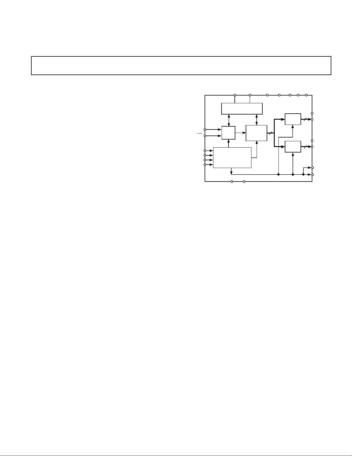
FUNCTIONAL BLOCK DIAGRAM
IN
IN
REFINREF
REFERENCE
T/H
TIMING AND
SYNCHRONIZATION
DFS I/P
OUT
ADC
10-BIT
CORE
AGND
10
AD9410
V
DGND
D
AD9410
PORT
A
PORT
B
V
V
DD
CC
OR
A
10
D9A–D0
A
OR
B
10
D9B–D0
B
DCO
DCO
GENERAL DESCRIPTION
The AD9410 is a 10-bit monolithic sampling analog-to-digital
converter with an on-chip track-and-hold circuit and is optimized for high-speed conversion and ease of use. The product
operates at a 210 MSPS conversion rate, with outstanding
dynamic performance over its full operating range.
The ADC requires a 5.0 V and 3.3 V power supply and up to a
210 MHz differential clock input for full performance operation.
No external reference or driver components are required for many
applications. The digital outputs are TTL/CMOS-compatible,
and separate output power supply pins also support interfacing
with 3.3 V logic.
The clock input is differential and TTL/CMOS-compatible. The
10-bit digital outputs can be operated from 3.3 V (2.5 V to 3.6 V)
supplies. Two output buses support demultiplexed data up to
105 MSPS rates, and binary or two’s complement output coding
format is available. A data sync function is provided for timingdependent applications. An output clock simplifies interfacing to
external logic. The output data bus timing is selectable for parallel
or interleaved mode, allowing for flexibility in latching output data.
Fabricated on an advanced BiCMOS process, the AD9410
is available in an 80-lead surface-mount plastic package
(PowerQuad
®
2) specified over the industrial temperature range
(–40°C to +85°C).
PRODUCT HIGHLIGHTS
High Resolution at High Speed—The architecture is specifically
designed to support conversion up to 210 MSPS with outstanding dynamic performance.
Demultiplexed Output—Output data is decimated by two and
provided on two data ports for ease of data transport.
Output Data Clock—The AD9410 provides an output data
clock synchronous with the output data, simplifying the timing
between data and other logic.
Data Synchronization—A DS input is provided to allow for
synchronization of two or more AD9410s in a system, or
to synchronize data to a specific output port in a single
AD9410 system.
PowerQuad is a registered trademark of Amkor Electronics, Inc.
REV. 0
Information furnished by Analog Devices is believed to be accurate and
reliable. However, no responsibility is assumed by Analog Devices for its
use, nor for any infringements of patents or other rights of third parties
which may result from its use. No license is granted by implication or
otherwise under any patent or patent rights of Analog Devices.
One Technology Way, P.O. Box 9106, Norwood, MA 02062-9106, U.S.A.
Tel: 781/329-4700 World Wide Web Site: http://www.analog.com
Fax: 781/326-8703 © Analog Devices, Inc., 2000

AD9410–SPECIFICATIONS
(VDD = 3.3 V, VD = 3.3 V, VCC = 5.0 V; 2.5 V external reference; AIN = –0.5 dBFS; Clock input = 210 MSPS;
DC SPECIFICATIONS
Parameter Temp Level Min Typ Max Unit
RESOLUTION 10 Bits
DC ACCURACY
No Missing Codes
Differential Nonlinearity 25°C I –1.0 ±0.5 +1.25 LSB
Integral Nonlinearity 25°C I –2.5 ±1.65 +2.5 LSB
Gain Error 25°C I –6.0 0 +6.0 % FS
Gain Tempco Full V 130 ppm/°C
ANALOG INPUT
Input Voltage Range (With Respect to AIN) Full V ±768 mV p-p
Common-Mode Voltage Full V 3.0 V
Input Offset Voltage 25°C I –15 +3 +15 mV
Reference Voltage Full VI 2.4 2.5 2.6 V
Reference Tempco Full V 50 ppm/°C
Input Resistance Full VI 610 875 1250 Ω
Input Capacitance 25°CV 3 pF
Analog Bandwidth, Full Power 25°C V 500 MHz
POWER SUPPLY
Power Dissipation AC
Power Dissipation DC
3
I
VCC
3
I
VD
Power Supply Rejection Ratio PSRR 25°C I –7.5 +0.5 +7.5 mV/V
NOTES
1
Package heat slug should be attached when operating at greater than 70°C ambient temperature.
2
Encode = 210 MSPS, AIN = –0.5 dBFS 10 MHz sine wave, I
3
Encode = 210 MSPS, AIN = dc, outputs not switching.
Specifications subject to change without notice.
1
TA = 25C; unless otherwise noted.)
2
3
Test
Full IV Guaranteed
Full VI –1.0 +1.5 LSB
Full VI –3.0 +3.0 LSB
Full VI –20 +20 mV
25°C V 2.1 W
Full VI 2.0 2.4 W
Full VI 128 145 mA
Full VI 401 480 mA
= 31 mA typical at C
VDD
LOAD
= 5 pF.
(VDD = 3.3 V, VD = 3.3 V, VCC = 5.0 V; 2.5 V external reference; AIN = –0.5 dBFS; Clock
SWITCHING SPECIFICATIONS
input = 210 MSPS; TA = 25C; unless otherwise noted.)
Test
Parameter Temp Level Min Typ Max Unit
SWITCHING PERFORMANCE
Maximum Conversion Rate Full VI 210 MSPS
Minimum Conversion Rate Full IV 100 MSPS
Encode Pulsewidth High (t
Encode Pulsewidth Low (t
Aperture Delay (t
)25°C V 1.0 ns
A
)25°C IV 1.2 2.4 ns
EH
)25°C IV 1.2 2.4 ns
EL
Aperture Uncertainty (Jitter) 25°C V 0.65 ps rms
Output Valid Time (t
Output Propagation Delay (t
Output Rise Time (t
Output Fall Time (t
CLKOUT Propagation Delay
Data to DCO Skew (t
DS Setup Time (t
DS Hold Time (t
) Full VI 3.0 ns
V
)25°C V 1.8 ns
R
)25°C V 1.4 ns
F
PD–tCPD
SDS
) Full IV 0 ns
HDS
) Full VI 7.4 ns
PD
1
(t
) Full VI 2.6 4.8 6.4 ns
CPD
) Full IV 0 1 2 ns
) Full IV 0.5 ns
Interleaved Mode (A, B Latency) Full VI A = 6, B = 6 Cycles
Parallel Mode (A, B Latency) Full VI A = 7, B = 6 Cycles
NOTES
1
C
= 5 pF.
LOAD
Specifications subject to change without notice.
–2–
REV. 0

(VDD = 3.3 V, VD = 3.3 V, VCC = 5.0 V; 2.5 V external reference; AIN = –0.5 dBFS;
AD9410
DIGITAL SPECIFICATIONS
Parameter Temp Level Min Typ Max Unit
DIGITAL INPUTS
DFS, Input Logic “1” Voltage Full IV 4 V
DFS, Input Logic “0” Voltage Full IV 1 V
DFS, Input Logic “1” Current Full V 50 µA
DFS, Input Logic “0” Current Full V 50 µA
I/P Input Logic “1” Current
I/P Input Logic “0” Current
ENCODE, ENCODE Differential Input Voltage Full IV 0.4 V
ENCODE, ENCODE Differential Input Resistance Full V 1.6 kΩ
ENCODE, ENCODE Common-Mode Input Voltage
DS, DS Differential Input Voltage Full IV 0.4 V
DS, DS Common-Mode Input Voltage Full V 1.5 V
Digital Input Pin Capacitance 25°CV 3 pF
DIGITAL OUTPUTS
Logic “1” Voltage (V
Logic “0” Voltage (V
Output Coding Binary or Two’s Complement
NOTES
1
I/P pin Logic “1” = 5 V, Logic “0” = GND. It is recommended to place a series 2.5 kΩ (±10%) resistor to VDD when setting to Logic “1” to limit input current.
2
See Encode Input section in Applications section.
Specifications subject to change without notice.
AC SPECIFICATIONS
1
1
= 3.3 V) Full VI V
DD
= 3.3 V) Full VI 0.05 V
DD
(V
TA = 25C; unless otherwise noted.)
Clock input = 210 MSPS; TA = 25C; unless otherwise noted.)
Test
Full V 400 µA
Full V 1 µA
2
Full V 1.5 V
– 0.05 V
DD
= 3.3 V, VD = 3.3 V, VCC = 5.0 V; 2.5 V external reference; AIN = –0.5 dBFS; Clock input = 210 MSPS;
DD
Test
Parameter Temp Level Min Typ Max Unit
DYNAMIC PERFORMANCE
Transient Response 25°CV 2 ns
Overvoltage Recovery Time 25°CV 2 ns
Signal-to-Noise Ratio (SNR)
(Without Harmonics)
f
= 10.3 MHz 25°C I 52.5 55 dB
IN
= 82 MHz 25°C I 52 54 dB
f
IN
f
= 160 MHz 25°CV 53 dB
IN
Signal-to-Noise Ratio (SINAD)
(With Harmonics)
f
= 10.3 MHz 25°C I 51 54 dB
IN
f
= 82 MHz 25°C I 50 53 dB
IN
= 160 MHz 25°CV 52 dB
f
IN
Effective Number of Bits
f
= 10.3 MHz 25°C I 8.3 8.8 Bits
IN
f
= 82 MHz 25°C I 8.1 8.6 Bits
IN
= 160 MHz 25°C V 8.4 Bits
f
IN
Second Harmonic Distortion
f
= 10.3 MHz 25°C I –56 –65 dBc
IN
f
= 82 MHz 25°C I –55 –63 dBc
IN
= 160 MHz 25°C V –65 dBc
f
IN
Third Harmonic Distortion
f
= 10.3 MHz 25°C I –58 –69 dBc
IN
f
= 82 MHz 25°C I –57 –67 dBc
IN
= 160 MHz 25°C V –62 dBc
f
IN
Spurious Free Dynamic Range (SFDR)
f
= 10.3 MHz 25°C I 56 61 dBc
IN
f
= 82 MHz 25°C I 54 60 dBc
IN
= 160 MHz 25°C V 58 dBc
f
IN
Two-Tone Intermod Distortion IMD
f
= 80.3 MHz, f
IN1
NOTES
1
IN1, IN2 level = –7 dBFS.
Specifications subject to change without notice.
= 81.3 MHz 25°C V 58 dBFS
IN2
REV. 0
1
–3–

AD9410
DATA N+3DATA N+1
V
t
DATA N+1
SAMPLE N+5
SAMPLE N+4
SAMPLE N+3
SAMPLE N+6
SAMPLE N+2
SAMPLE N+1
S
1/f
DATA N DATA N+2
PD
t
INVALID
INVALID
INVALID
INVALID
SDS
t
INTERLEAVED DATA OUT
INVALID INVALID INVALID INVALID
PARALLEL DATA OUT
DATA N DATA N+2
t
INVALIDINVALIDINVALID
CPD
SAMPLE N
SAMPLE N–1
AIN
EL
t
A
t
EH
t
HDS
t
SAMPLE N–2
DS
DS
ENCODE
ENCODE
STATIC INVALID INVALID
D7D0
PORT A
STATIC
D7D0
PORT B
STATIC
D7D0
PORT A
STATIC
D7D0
PORT B
DCO
STATIC
DCO
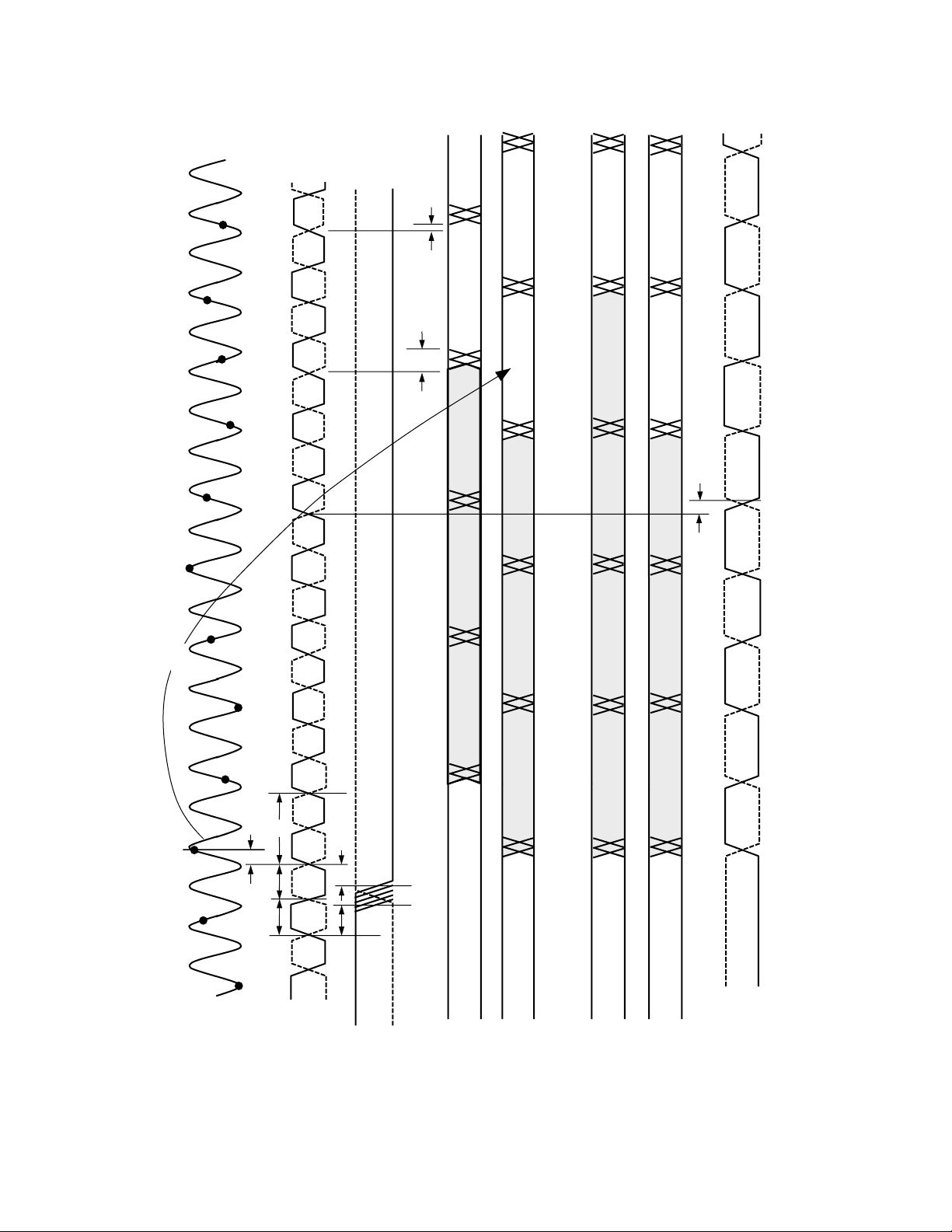
Figure 1. Timing Diagram
–4–
REV. 0

AD9410
ABSOLUTE MAXIMUM RATINGS
VD, V
CC, VDD
. . . . . . . . . . . . . . . . . . . . . . . . . . . . . . . . . . . 6 V
Analog Inputs . . . . . . . . . . . . . . . . . . . . . 0 V to V
Digital Inputs . . . . . . . . . . . . . . . . . . . . . 0 V to V
VREF IN . . . . . . . . . . . . . . . . . . . . . . . . . . 0 V to V
1
+ 0.5 V
CC
+ 0.5 V
DD
+ 0.5 V
D
Digital Output Current . . . . . . . . . . . . . . . . . . . . . . . . 20 mA
Operating Temperature . . . . . . . . . . . . . . . . –55°C to +125°C
Storage Temperature . . . . . . . . . . . . . . . . . . –65°C to +150°C
Maximum Junction Temperature
NOTES
1
Absolute maximum ratings are limiting values to be applied individually, and
beyond which the serviceability of the circuit may be impaired. Functional
operability is not necessarily implied. Exposure to absolute maximum rating
conditions for an extended period of time may affect device reliability. Stresses
above those listed under Absolute Maximum Ratings may cause permanent
damage to the device. This is a stress rating only; functional operation of the device
at these or any other conditions outside of those indicated in the operation sections
of this specification is not implied.
2
Typical θJA = 22°C/W (heat slug not soldered), typical θJA = 16°C/W (heat slug
soldered), for multilayer board in still air with solid ground plane.
2
. . . . . . . . . . . . . . . . 150°C
ORDERING GUIDE
Temperature Package Package
Model Range Description Option
AD9410BSQ –40°C to +85°C PowerQuad 2 SQ-80
AD9410/PCB 25°C Evaluation Board
EXPLANATION OF TEST LEVELS
Test Level
I. 100% production tested.
II. 100% production tested at 25°C and sample tested at
specified temperatures.
III. Sample tested only.
IV. Parameter is guaranteed by design and characterization
testing.
V. Parameter is a typical value only.
VI. 100% production tested at 25°C; guaranteed by design and
characterization testing for industrial temperature range.
CAUTION
ESD (electrostatic discharge) sensitive device. Electrostatic charges as high as 4000 V readily
accumulate on the human body and test equipment and can discharge without detection. Although
the AD9410 features proprietary ESD protection circuitry, permanent damage may occur on
devices subjected to high-energy electrostatic discharges. Therefore, proper ESD precautions are
recommended to avoid performance degradation or loss of functionality.
WARNING!
ESD SENSITIVE DEVICE
REV. 0
–5–

AD9410
PIN FUNCTION DESCRIPTIONS
Pin No. Mnemonic Function
1, 2, 8, 9, 12, 13, 16, 17, 20, 21, 24, AGND Analog Ground.
27, 28, 29, 30, 71, 72, 73, 74, 77, 78
3, 7, 14, 15 V
4 REF
5 REF
CC
OUT
IN
6 DNC Do Not Connect.
10 A
IN
11 AIN Analog Input—Complement.
18 ENCODE Clock Input—True.
19 ENCODE Clock Input—Complement.
22 DS Data Sync (Input)—True. Tie LOW if not used.
23 DS Data Sync (Input)—Complement. Float and decouple with 0.1 µF
25, 26, 31, 32, 69, 70, 75, 76 V
D
33, 40, 49, 52, 59, 68 DGND Digital Ground.
34, 41, 48, 53, 60, 67 V
35–39 D
42–46 D
47 OR
DD
B0–DB4
B5–DB9
B
50 DCO Clock Output—Complement.
51 DCO Clock Output—True.
54–58 D
61–65 D
66 OR
A0–DA4
A5–DA9
A
79 DFS Data Format Select. HIGH = Two’s Complement, LOW = Binary.
80 I/P Interleaved or Parallel Output Mode. Low = Parallel Mode, High =
5 V Supply. (Regulate to within ±5%.)
Internal Reference Output.
Internal Reference Input.
Analog Input—True.
capacitor if not used.
3.3 V Analog Supply. (Regulate to within ±5%.)
3.3 V Digital Output Supply. (2.5 V to 3.6 V)
Digital Data Output for Channel B. (LSB = DB0.)
Digital Data Output for Channel B. (MSB = DB9.)
Data Overrange for Channel B.
Digital Data Output for Channel A. (LSB = DA0.)
Digital Data Output for Channel A. (MSB = DA9.)
Data Overrange for Channel A.
Interleaved Mode. If tying high, use a current limiting series resistor
(2.5 kΩ) to the 5 V supply.
–6–
REV. 0
 Loading...