Low Power HDMI Display Interface
FEATURES
HDMI interface
Supports high bandwidth digital content protection
RGB to YCrCb 2-way color conversion
1.8 V/3.3 V power supply
76-ball BGA package
RGB and YCrCb output formats
Digital video interface
HDMI 1.2a, DVI 1.0
80 MHz HDMI receiver
Supports high bandwidth digital content protection
(HDCP 1.1)
Digital audio interface
HDMI 1.2a-compatible audio interface
S/PDIF (IEC60958-compatible) digital audio output
Multichannel I
APPLICATIONS
Portable low power TV
HDTV
Projectors
LCD monitor
2
S audio output (up to 8 channels)
RTERM
DDC_SCL
DDC_SDA
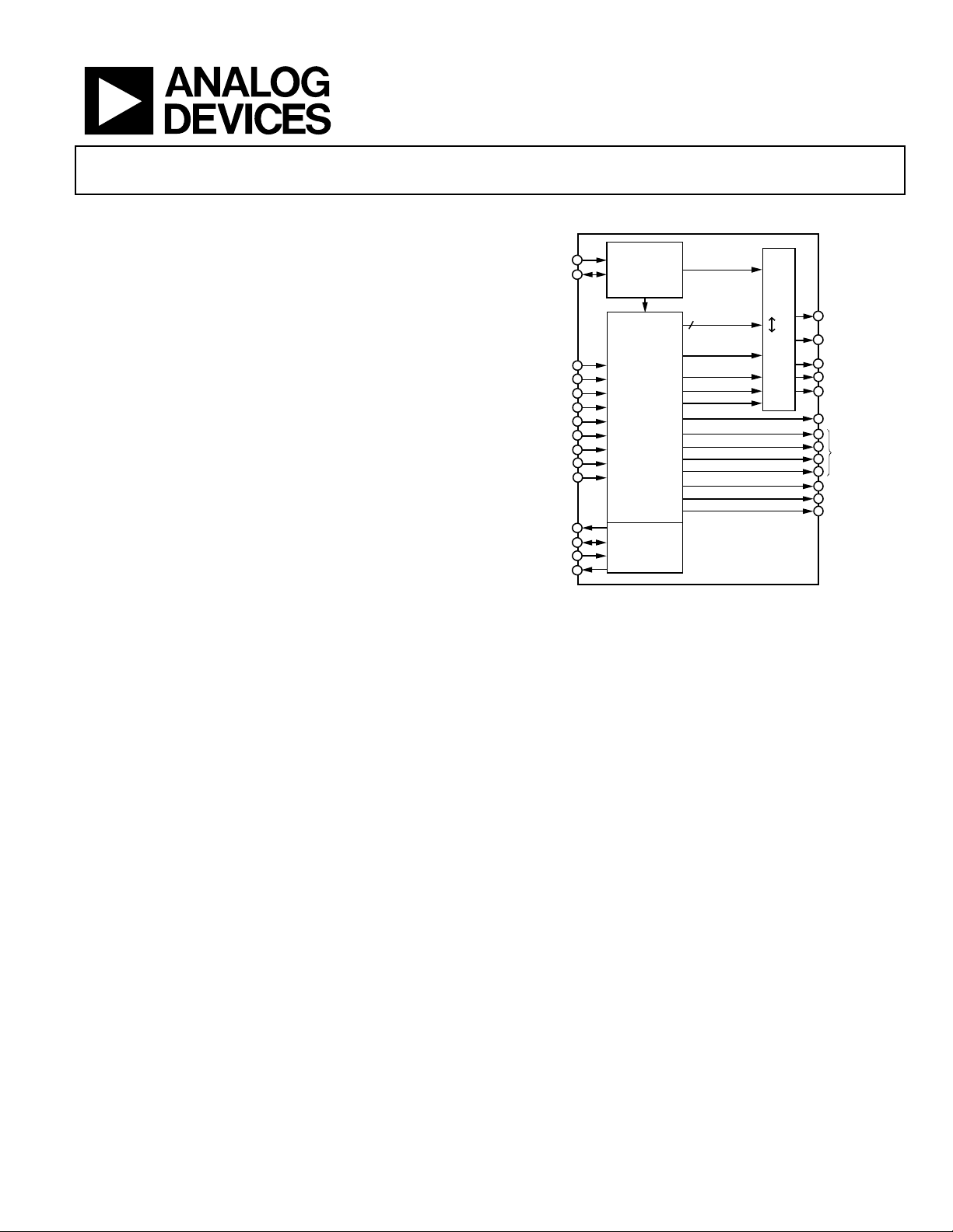
FUNCTIONAL BLOCK DIAGRAM
SERIAL
SCL
SDA
Rx0+
Rx0–
Rx1+
Rx1–
Rx2+
Rx2–
RxC+
RxC–
MCL
MDA
REGISTER
AND
POWER
MANAGEMENT
HDMI
RECEIVER
HDCP
R/G/B 8 × 3
OR YCrCb
DATACK
H
SYNC
V
SYNC
DE
Figure 1.
AD9393
AD9393
D[23:0]
DCLK
YCrCb RGB
HSOUT
VSOUT
COLORSPACE CONVERTER
DE
SPDIF
8-CHANNEL
2
I
MCLK
SCLK
LRCLK
S
08043-001
GENERAL DESCRIPTION
The AD9393 offers a High-Definition Multimedia Interface
(HDMI™) receiver integrated on a single chip. Support is also
included for high bandwidth digital content protection (HDCP).
The AD9393 contains a HDMI 1.2a-compatible receiver and
supports HDTV formats (up to 720p or 1080i) and displays
resolutions up to XGA (1024 × 768 @ 75 Hz). The receiver
features an intrapair skew tolerance of up to one full clock
cycle. With the inclusion of HDCP, displays may now receive
encrypted video content. The AD9393 allows for authentication
Rev. 0
Information furnished by Analog Devices is believed to be accurate and reliable. However, no
responsibility is assumed by Analog Devices for its use, nor for any infringements of patents or other
rights of third parties that may result from its use. Specifications subject to change without notice. No
license is granted by implication or otherwise under any patent or patent rights of Analog Devices.
Trademarks and registered trademarks are the property of their respective owners.
of a video receiver, decryption of encoded data at the receiver,
and renewability of that authentication during transmission as
specified by the HDCP 1.1 protocol.
Fabricated in an advanced CMOS process, the AD9393 is
provided in a space-saving 76-ball, surface-mount, Pb-free,
ball grid array (BGA) and is specified over the −10°C to
+80°C temperature range.
One Technology Way, P.O. Box 9106, Norwood, MA 02062-9106, U.S.A.
Tel: 781.329.4700 www.analog.com
Fax: 781.461.3113 ©2009 Analog Devices, Inc. All rights reserved.

AD9393
TABLE OF CONTENTS
Features .............................................................................................. 1
Applications ....................................................................................... 1
Functional Block Diagram .............................................................. 1
General Description ......................................................................... 1
Revision History ............................................................................... 2
Specifications ..................................................................................... 3
Electrical Characteristics ............................................................. 3
Digital Interface Electrical Characteristics ............................... 4
Absolute Maximum Ratings ............................................................ 5
Explanation of Test Levels ........................................................... 5
ESD Caution .................................................................................. 5
Pin Configuration and Function Descriptions ............................. 6
Design Guide ..................................................................................... 8
General Description ..................................................................... 8
Digital Inputs ................................................................................ 8
Serial Control Port ....................................................................... 8
Output Signal Handling ............................................................... 8
Power Management ...................................................................... 8
Timing ............................................................................................ 9
HDMI Receiver ............................................................................. 9
DE Generator ................................................................................ 9
4:4:4 to 4:2:2 Filter ........................................................................ 9
Audio PLL Setup ......................................................................... 10
Audio Board Level Muting ........................................................ 11
Output Data Formats ................................................................. 11
2-Wire Serial Register Map ........................................................... 12
2-Wire Serial Control Register Details ........................................ 22
Chip Identification ..................................................................... 22
BT656 Generation ...................................................................... 24
Color Space Conversion ............................................................ 25
2-Wire Serial Control Port ............................................................ 31
Data Transfer via Serial Interface ............................................. 31
Serial Interface Read/Write Examples ..................................... 32
PCB Layout Recommendations .................................................... 33
Power Supply Bypassing ............................................................ 33
Outputs (Both Data and Clocks) .............................................. 33
Digital Inputs .............................................................................. 33
Color Space Converter (CSC) Common Settings ...................... 34
HDTV YCrCb (0 to 255) to RGB (0 to 255) (Default Setting
for AD9393) ................................................................................ 34
HDTV YCrCb (16 to 235) to RGB (0 to 255)......................... 34
SDTV YCrCb (0 to 255) to RGB (0 to 255) ............................ 34
SDTV YCrCb (16 to 235) to RGB (0 to 255) .......................... 35
RGB (0 to 255) to HDTV YCrCb (0 to 255) ........................... 35
RGB (0 to 255) to HDTV YCrCb (16 to 235)......................... 35
RGB (0 to 255) to SDTV YCrCb (0 to 255) ............................ 36
RGB (0 to 255) to SDTV YCrCb (16 to 235) .......................... 36
Outline Dimensions ....................................................................... 37
Ordering Guide .......................................................................... 37
REVISION HISTORY
10/09—Revision 0: Initial Version
Rev. 0 | Page 2 of 40

AD9393
SPECIFICATIONS
ELECTRICAL CHARACTERISTICS
VDD, VD = 3.3 V, DVDD = PVDD = 1.8 V, unless otherwise noted.
Table 1.
Parameter Temp Test Level Min Typ Max Unit
DIGITAL INPUTS (5 V Tolerant)
Input Voltage, High (VIH) Full VI 2.6 V
Input Voltage, Low (VIL) Full VI 0.8 V
Input Current, High (IIH) Full V −82 μA
Input Current, Low (IIL) Full V 82 μA
Input Capacitance 25°C V 3 pF
DIGITAL OUTPUTS
Output Voltage, High (VOH) Full VI VDD − 0.1 V
Output Voltage, Low (VOL) Full VI 0.4 V
Duty Cycle, DCLK Full V 45 50 55 %
Output Coding Binary
THERMAL CHARACTERISTICS
θJA Junction-to-Ambient V 59 °C/W
θJC Junction-to-Case V 15.2 °C/W
Rev. 0 | Page 3 of 40

AD9393
DIGITAL INTERFACE ELECTRICAL CHARACTERISTICS
VDD = VD =3.3 V, DVDD = PVDD = 1.8 V, unless otherwise noted.
Table 2.
Parameter
DC DIGITAL I/O Specifications
High-Level Input Voltage (VIH) VI 2.5 V
Low-Level Input Voltage (VIL) VI 0.8 V
High-Level Output Voltage (VOH) VI VDD − 0.1 V
Low-Level Output Voltage (VOL) VI VDD − 0.1 0.1 V
DC SPECIFICATIONS
Output High Level IV Output drive = high strength 36 mA
I
(V
= VOH) IV Output drive = low strength 24 mA
OHD
OUT
Output Low Level IV Output drive = high strength 12 mA
I
(V
= VOL) IV Output drive = low strength 8 mA
OLD
OUT
DCLK High Level IV Output drive = high strength 40 mA
V
(V
= VOH) IV Output drive = low strength 20 mA
OHC
OUT
DCLK Low Level IV Output drive = high strength 30 mA
V
(V
= VOL) IV Output drive = low 15 mA
OLC
OUT
Differential Input Voltage, Single-Ended Amplitude IV 75 700 mV
POWER SUPPLY
VD IV 3.15 3.3 3.47 V
VDD IV 1.7 3.3 347 V
DVDD IV 1.7 1.8 1.9 V
PVDD IV 1.7 1.8 1.9 V
Power—54 MHz, YCrCb 422, CSC Disabled 485 mW
Supply Current (Worst Pattern)1
IVD V 95 mA
I
V 18 mA
VDD
2
I
V 51 mA
DVDD
I
V 26 mA
PVDD
Power—74.25 MHz, RGB, CSC Disabled 593 mW
Supply Current (Worst Pattern)1
IVD V 109 mA
I
V 38 mA
VDD
I
V 66 mA
DVDD
I
V 26 mA
PVDD
Power-Down Power VI 130 mW
AC SPECIFICATIONS
Intrapair (+ to −) Differential Input Skew (t
Channel-to-Channel Differential Input Skew (t
Low-to-High Transition Time for Data and Controls (D
) IV 0.4 t
DPS
) IV 0.6 t
CCS
LHT
IV Output drive = low; CL = 5 pF ps
Low-to-High Transition Time for DCLK (D
) IV Output drive = high; CL = 10 pF 1000 ps
LHT
IV Output drive = low; CL = 5 pF ps
High-to-Low Transition Time for Data and Controls (D
HLT
IV Output drive = low; CL = 5 pF ps
High-to-Low Transition Time for DCLK (D
) IV Output drive = high; CL = 10 pF 1000 ps
HLT
IV Output drive = low; CL = 5 pF ps
Clock-to-Data Skew3 (t
) IV −0.5 +2.0 ns
SKEW
Duty Cycle, DCLK3 IV 45 50 %
DCLK Frequency (f
1
Worst-case pattern is alternating black and white pixels.
2
DCLK load = 10 pF, data load = 5 pF.
3
Drive strength = high.
) VI 20 80 MHz
CIP
Test
Level
Conditions Min Typ Max Unit
) IV Output drive = high; CL = 10 pF 1000 ps
) IV Output drive = high; CL = 10 pF 1000 ps
Rev. 0 | Page 4 of 40
BIT
PIXEL
AD9393
ABSOLUTE MAXIMUM RATINGS
Table 3.
Parameter Rating
VD 3.6 V
VDD 3.6 V
DVDD 1.98 V
PVDD 1.98 V
Digital Inputs 5 V to 0.0 V
Digital Output Current 20 mA
Operating Temperature Range −25°C to +85°C
Storage Temperature Range −65°C to +150°C
Maximum Junction Temperature 150°C
Maximum Case Temperature 150°C
Stresses above those listed under Absolute Maximum Ratings
may cause permanent damage to the device. This is a stress
rating only; functional operation of the device at these or any
other conditions above those indicated in the operational
section of this specification is not implied. Exposure to absolute
maximum rating conditions for extended periods may affect
device reliability.
EXPLANATION OF TEST LEVELS
I 100% production tested.
II 100% production tested at 25°C and sample tested at
specified temperatures.
III Sample tested only.
IV Parameter is guaranteed by design and characterization
testing.
V Parameter is a typical value only.
VI 100% production tested at 25°C; guaranteed by design
and characterization testing.
ESD CAUTION
Rev. 0 | Page 5 of 40
AD9393
G
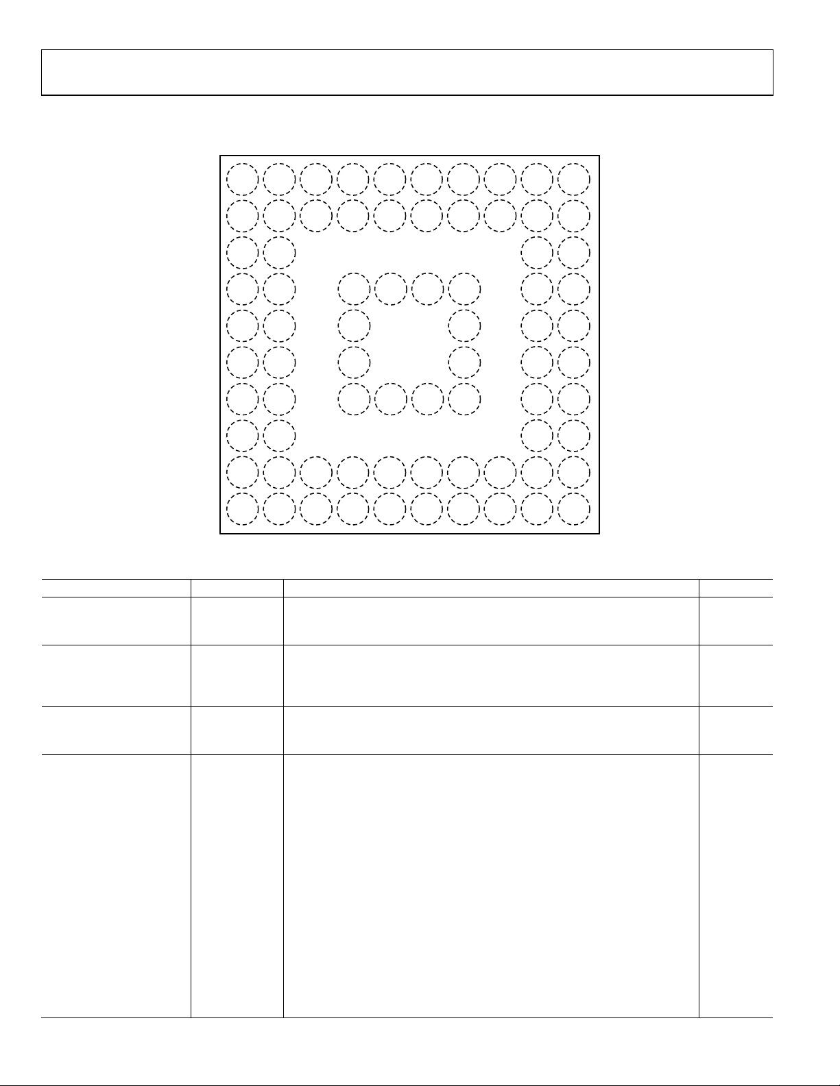
PIN CONFIGURATION AND FUNCTION DESCRIPTIONS
12345678910
D14 D15 D16 D18 D20 D22 DCLK
A
D13
B
C
D
E
F
H
J
K
D12 D17 D19 D21 D23 DE
D10
D11
D9
D8
D7
D6
D5
D4
D3
D2
D1
D0
GND
MCLK I2S3 I2S2 I2S1 I2S0
RxC–
RxC+ GND Rx0– Rx0+ GND Rx1–
V
DDVDD
GND V
(Not to S cale)
GND V
SCLK
LRCLK
AD9393
TOP VIEW
GND GND
DVDDDV
HSOUT
VSOUT
D
D
DD
SPDIF
RTERM
Rx1+ GND Rx2–
O/E SDA
PD SCL
GND GND
GND FILT
GND GND
PV
MDA
DD
PV
MCL
DD
DDC_
GND
SCL
DDC_
Rx2+
SDA
08043-002
Figure 2. Pin Configuration
Table 4. Complete Pin List
Pin No. Mnemonic Description Value
Inputs
B9 PD
Power-Down Control. Power-Down Control/Three-State Control. The function
3.3 V CMOS
of this pin is programmable via Register 0x26[2:1].
Digital Video Data Inputs
K5, K4, K8, K7, J10, K10
Rx0+, Rx0−,
Rx1+, Rx1−,
Rx2+, Rx2−
Digital Input Channel x True/Complement. These six pins receive three pairs of
transition minimized differential signaling (TMDS ) pixel data (at 10× the pixel
rate) from a digital graphics transmitter.
TMDS
Digital Video Clock Inputs
K2, K1 RxC+, RxC−
Digital Data Clock True/Complement. This clock pair receives a TMDS clock at
TMDS
1× pixel data rate.
Outputs
B6, A6, B5, A5, B4,
A4, B3, A3, A2, A1,
B1, B2, C1, C2, D1,
D2, E1, E2, F1, F2,
G1, G2, H1, H2
A7 DCLK
D[23:0]
Data Outputs. In RGB,
D[23:16] = Red[7:0]
D[15:8] = Green[7:0]
D[7:0] = Blue[7:0]
See Tab le 6
Data Output Clock. This is the main clock output signal used to strobe the
V
DD
VDD
output data and HSOUT into external logic. Four possible output clocks can
be selected with Register 0x25[7:6]. These are related to the pixel clock (½×
pixel clock, 1× pixel clock, 2× frequency pixel clock, and a 90° phase shifted
pixel clock). They are produced by the internal PLL clock generator and are
synchronous with the pixel clock. The polarity of DCLK can also be inverted via
Register 0x24[0].
A8 HSOUT
HSYNC Output Clock (Phase-Aligned with DCLK). Horizontal sync output. A
VDD
reconstructed and phase-aligned version of the HSYNC input. Both the
polarity and duration of this output can be programmed via serial bus
registers. By maintaining alignment with DCLK and data, data timing with
respect to horizontal sync can always be determined.
Rev. 0 | Page 6 of 40

AD9393
Pin No. Mnemonic Description Value
B8 VSOUT
VSYNC Output Clock (Phase-Aligned with DCLK). Vertical Sync Output. The
separated VSYNC from a composite signal or a direct passthrough of the
VSYNC signal. The polarity of this output can be controlled via the serial bus
bit (Register 0x24[6]).
A9 O/E
Odd/Even Field Output for Interlaced Video. This output identifies whether the
current field (in an interlaced signal) is odd or even. The polarity of this signal
is programmable via Register 0x24[4].
References
D10 FILT
Connection for External Filter Components for Audio PLL. For proper operation,
the audio clock generator PLL requires an external filter. Connect the filter
shown in Figure 6 to this pin. For optimal performance, minimize noise and
parasitics on this node. For more information, see the PCB Layout
Recommendations section.
Power Supply1
E7, F7 VD
HDMI Terminator Power Supply
(3.3 V). These pins supply power to the HDMI
terminators. They should be as quiet and filtered as possible.
D4, D5
VDD
Digital Output Power Supply
(1.8 V to 3.3 V). A large number of output pins (up
to 27) switching at high speed (up to 80 MHz) generates many power supply
transients (noise). These supply pins are identified separately from the VD pins,
so output noise transferred into the sensitive circuitry can be minimized. If the
AD9393 is interfacing with lower voltage logic, VDD can be connected to a
lower supply voltage (as low as 1.8 V) for compatibility.
F9, G9 PVDD
PLL Power Supply (1.8 V). The most sensitive portion of the AD9393 is the
clock generation circuitry. These pins provide power to the clock PLL and help
the user design for optimal performance. The user should provide quiet,
noise-free power to these pins.
G6, G7 DVDD
Digital Logic Power Supply (1.8 V). These pins supply power to the digital
logic.
C9, C10, D6, D7, D9, E4,
E9, E10,
F4, H10, J1, K3, K6, K9
GND
Ground. The ground return for all circuitry on chip. It is recommended that the
AD9393 be assembled on a single solid ground plane, with careful attention
to ground current paths.
Control
A10 SDA
Serial Port Data I/O for Programming the AD9393 Registers. The I
2
C address is
Address 0x98.
B10 SCL Serial Port Data Clock for Programming the AD9393 Registers. 3.3 V CMOS
HDCP
H9 DDC_SCL HDCP Slave Serial Port Data Clock for HDCP Communications to Transmitter. 3.3 V CMOS
J9 DDC_SDA
HDCP Slave Serial Port Data I/O for HDCP Communications to Transmitter. The
I2C address is Address 0x74 or Address 0x76.
F10 MDA Master Serial Port I/O to EEPROM with HDCP Keys—I2C Address is 0xA0. 3.3 V CMOS
G10 MCL Master Serial Port Data Clock to EEPROM with HDCP Keys. 3.3 V CMOS
Audio Data Outputs
J7 S/PDIF S/PDIF Digital Audio Output. VDD
J6 I2S0 I2S Audio (Channel 1, Channel 2). Channel 0 and Channel 1 Audio Output. VDD
J5 I2S1 I2S Audio (Channel 3, Channel 4). Channel 2 and Channel 3 Audio Output. VDD
J4 I2S2 I2S Audio (Channel 5, Channel 6). Channel 4 and Channel 5 Audio Output. VDD
J3 I2S3 I2S Audio (Channel 7, Channel 8). Channel 6 and Channel 7 Audio Output. VDD
J2 MCLK Audio Master Clock Output for S/PDIF Data. VDD
G4 SCLK Audio Serial Clock Output for I2S Data. VDD
G5 LRCLK Data Output Clock for Left and Right Audio Channels. VDD
Data Enable
B7 DE Data Enable for Active Data Pixels. 3.3 V CMOS
RTERM
J8 RTERM
Sets Internal Termination Resistance. Place a 500 Ω (1% tolerance) resistor from
this pin to ground. This sets the internal termination of TMDS lines to 50 Ω.
1
The supplies should be sequenced such that VD and VDD are never less than 300 mV below DVDD. At no time should DVDD be more than 300 mV greater than VD or VDD.
Rev. 0 | Page 7 of 40
V
DD
VDD
PVDD
3.3 V
1.8 V to 3.3
V
1.8 V
1.8 V
0 V
3.3 V CMOS
3.3 V CMOS
500 Ω

AD9393
DESIGN GUIDE
GENERAL DESCRIPTION
The AD9393 is a fully integrated solution for receiving DVI/
HDMI signals and is capable of decoding HDCP-encrypted
signals through connections to an external EEPROM. The
circuit is ideal for providing an interface for HDTV monitors
or as the front end to high performance video scan converters.
Implemented in a high performance CMOS process, the
interface can capture signals with pixel rates of up to 80 MHz.
The AD9393 includes all necessary circuitry for decoding
TMDS signaling including those encrypted with HDCP.
Included in the output formatting is a color space converter
(CSC), which accommodates any input color space and can
output any color space. All controls are programmable via a
2-wire serial interface. Full integration of these sensitive mixed
signal functions makes system design straight forward and less
sensitive to the physical and electrical environment.
DIGITAL INPUTS
The digital control inputs (I2C) on the AD9393 operate to 3.3 V
CMOS levels. In addition, all digital inputs except the TMDS
inputs (HDMI/DVI) are 5 V tolerant. Applying 5 V to them
does not cause any damage. The TMDS input pairs (Rx0±,
Rx1±, Rx2±, and RxC±) must maintain a 100 Ω differential
impedance (through proper PCB layout) from the connector to
the input where they are internally terminated (50 Ω to 3.3 V).
If additional ESD protection is desired, using a low capacitance
ESD protection varistor offers 8 kV of protection to the HDMI
TMDS lines.
SERIAL CONTROL PORT
The serial control port is designed for 3.3 V logic. However, it is
tolerant of 5 V logic signals.
OUTPUT SIGNAL HANDLING
The digital outputs operate from 1.8 V to 3.3 V (VDD).
POWER MANAGEMENT
To determine the correct power state, the AD9393 uses the
activity detect circuits, the active interface bits in the serial bus,
the active interface override bits, the power-down bit, and the
power-down ball. There are three power modes: full power,
auto power-down, and power-down.
Tabl e 5 summarizes how the AD9393 determines which power
mode to use and which circuitry is powered on/off in each of
these modes. The power-down command has first priority and
the automatic circuitry second priority. The power-down ball
(Ball B8—polarity set by Register 0x26[3]) can drive the chip
into two power-down options. Bit 2 of Register 0x26 controls
these two options. Bit 0 controls whether the chip is powered
down or the outputs are placed in high impedance mode. Bit 7
to Bit 4 of Register 0x26 control whether the outputs, Sony/
Philips digital interface (S/PDIF), or Inter-IC Sound bus (I
IIS) outputs are in high impedance mode or not. See the 2-Wire
Serial Control Register Detail section for the details.
2
S or
Table 5. Power-Down Mode Descriptions
Inputs
Mode
Full Power 1 X Everything
Auto Power-Down 1 1 Serial bus, sync activity detect, band gap reference
Power-Down 0 X Serial bus, sync activity detect, band gap reference
1
Power-down is controlled via Bit 0 in Register 0x26.
2
Auto power-down is controlled via Bit 7 in Register 0x27.
Power-On/Comments Power-Down1 Auto PD Enable2
Rev. 0 | Page 8 of 40
AD9393
TIMING
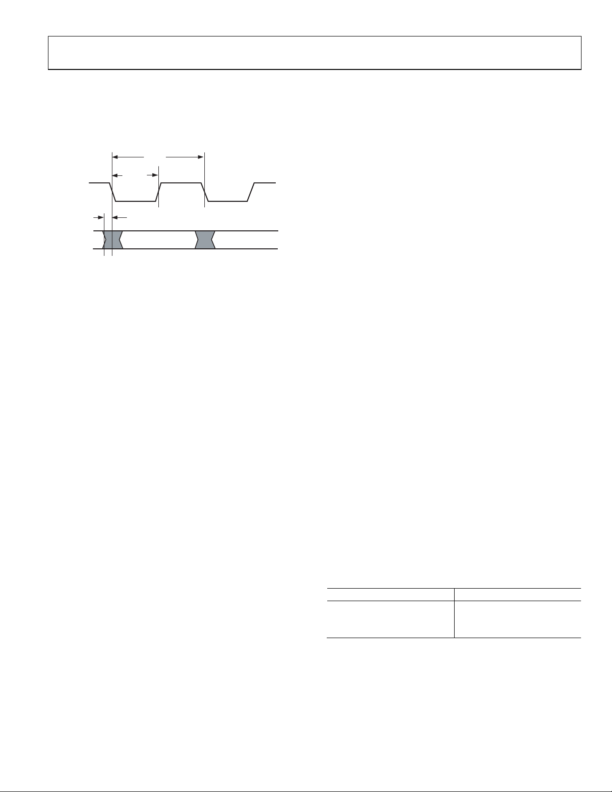
The output data clock signal is created so that its rising edge
always occurs between data transitions and can be used to latch
the output data externally.
Figure 3 shows the timing operation of the AD9393.
t
PER
t
DCYCLE
DATACK
t
SKEW
DATA
HSOUT
08043-003
Figure 3. Output Timing
HDMI RECEIVER
The HDMI receiver section of the AD9393 allows the reception
of a digital video stream (which is backward compatible with
DVI and able to accommodate video of various formats (RGB,
YCrCb 4:4:4, 4:2:2)). The receiver also allows up to eight channels
of audio. Infoframes are transmitted carrying information about
the video format, audio clocks, and many other items necessary
for a monitor to utilize fully the information stream available.
The earlier digital visual interface (DVI) format was restricted
to an RGB 24-bit color space only. Embedded in this data stream
were HSYNCs, VSYNCs, and display enable (DE) signals; but
no audio information. The HDMI specification allows transmission of all the DVI capabilities, but adds several YCrCb
formats that make the inclusion of a programmable color space
converter (CSC) a very desirable feature. With this feature, the
scaler following the AD9393 can specify that it always wishes to
receive a particular format, for instance, 4:2:2 YCrCb, regardless
of the transmitted mode. If RGB is sent, the CSC can easily
convert that to 4:2:2 YCrCb while relieving the scaler of this
task.
In addition, the HDMI specification supports the transmission
of up to eight channels of S/PDIF or I
mation is separated into packets and transmitted during the
video blanking periods along with specific information about
the clock frequency. Part of this audio information (audio
infoframe) tells the user how many channels of audio are being
transmitted, where the channels should be placed, information
regarding the source (make, model), and other data.
2
S audio. The audio infor-
DE GENERATOR
The AD9393 has an on-board generator for DE, for the start
of active video (SAV), and for the end of active video (EAV), all
of which are necessary for describing the complete data stream
for a BT656-compatible output. This signal alerts the following
circuitry, which are displayable video pixels.
4:4:4 TO 4:2:2 FILTER
The AD9393 contains a filter that allows it to convert a
signal from YCrCb 4:4:4 to YCrCb 4:2:2 while maintaining
the maximum accuracy and fidelity of the original signal.
Input Color Space to Output Color Space
The AD9393 can accept a wide variety of input formats and
either retain that format or convert to another. Input formats
supported are
• 4:4:4 YCrCb 8-bit
• 4:2:2 YCrCb 8-, 10-, and 12-bit
• RGB 8-bit
Output modes supported are
• 4:4:4 YCrCb 8-bit
• 4:2:2 YCrCb 8-, 10-, and 12-bit
• Dual 4:2:2 YCrCb 8-bit
Color Space Conversion (CSC) Matrix
The CSC matrix in the AD9393 consists of three identical
processing channels. In each channel, three input values are
multiplied by three separate coefficients. An offset value for
each row of the matrix and a scaling multiple for all values
are also included. Each value has a 13-bit, twos complement
resolution to ensure the signal integrity is maintained. The
CSC is designed to run at speeds up to 80 MHz supporting
resolutions up to 720p at 60 Hz. With any-to-any color space
support, formats such as RGB, YUV, YCrCb, and others are
supported by the CSC.
The main inputs, R
bit inputs from each channel. These inputs are based on the
input format detailed in Tabl e 30 to Tab l e 5 2 . The mapping of
these inputs to the CSC inputs is shown in Tab l e 6 .
Table 6. CSC Port Mapping
Input Channel CSC Input Channel
R/Cr (D[23:16]) RIN
Gr/Y (D[15:8]) GIN
B/Cb (D[7:0]) BIN
, GIN, and BIN, come from the 8-bit or 12-
IN
Rev. 0 | Page 9 of 40
AD9393
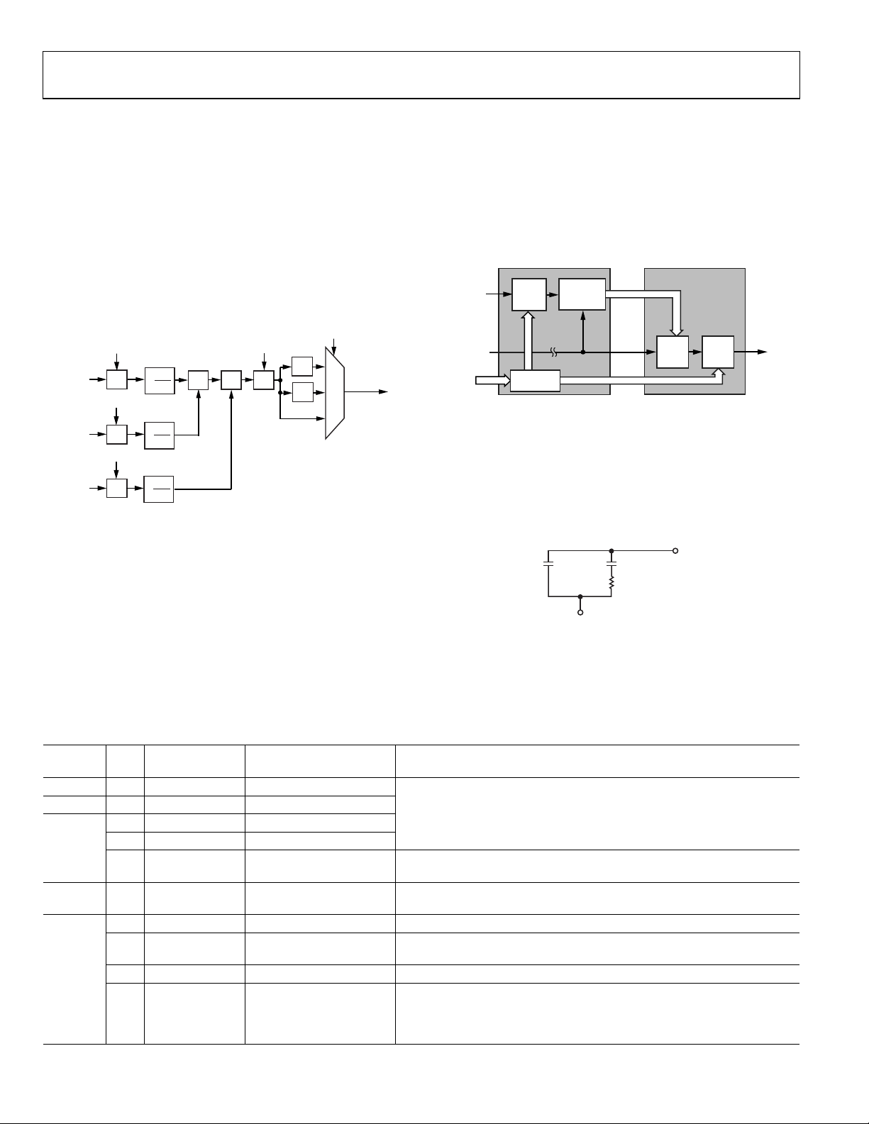
One of the three input channels is represented in Figure 4.
In each processing channel, the three inputs are multiplied
by three separate coefficients marked a1, a2, and a3. These
coefficients are divided by 4096 to obtain nominal values
ranging from −0.9998 to +0.9998. The variable labeled a4 is
used as an offset control. The CSC_MODE setting is the same
for all three processing channels. This multiplies all coefficients
and offsets by a factor of 2
CSC_MODE
.
The functional diagram for a single channel of the CSC (as
shown in Figure 4) is repeated for the remaining G and B
channels. The coefficients for these channels are b1, b2, b3,
b4, c1, c2, c3, and c4.
CSC_MODE[1:0]
a1[12:0]
[11:0]
R
IN
[11:0]
G
IN
[11:0]
B
IN
×
a2[12:0]
×
a3[12:0]
×
×
×
×
4096
4096
4096
1
+
1
1
a4[12:0]
×4
+
+
2
R
[11:0]
×2
OUT
1
0
8043-006
Figure 4. Single CSC Channel
A programming example and register settings for several
common conversions are listed in the Color Space Converter
(CSC) Common Settings section.
For a detailed functional description and more programming
examples that are compatible with the AD9393, refer to the
AN-795 Application Note, AD9880 Color Space Converter
User's Guide.
AUDIO PLL SETUP
Data contained in the audio infoframes (among other registers)
defines for the AD9393 HDMI receiver not only the type of
Table 7. Audio Register Settings
Recommended
Register Bits
0x01 [7:0] 0x00 PLL divisor (MSBs)
0x02 [7:4] 0x40 PLL divisor (LSBs)
0x03 [7:6] 01 VCO range
0x34 [5:4] 11
0x58 [7] 1 MCLK PLL enable This enables the analog PLL to be used for audio MCLK generation.
Setting
Function Comments
The video PLL is used for the audio clock circuit when in HDMI mode. This
is done automatically.
[5:3] 010 Charge pump current
[2] 1 PLL enable
In HDMI mode, this bit enables a lower frequency to be used for audio
MCLK generation.
Audio frequency mode
Allows the chip to determine the low frequency mode of the audio PLL.
override
[6:4] 001 MCLK PLL divisor
When the analog PLL is enabled for MCLK generation, another frequency
divider is provided; these bits set the divisor to 2.
[3] 0 N/CTS disable The N and CTS values should always be enabled.
[2:0] 0**
MCLK sampling
frequency
000 = 128 × f
001 = 256 × f
010 = 384 × f
011 = 512 × fS
audio, but also the sampling frequency (f
). The audio info-
S
frame also contains information about the N and CTS values
used to recreate the clock. With this information, it is possible
to regenerate the audio sampling frequency. The audio clock is
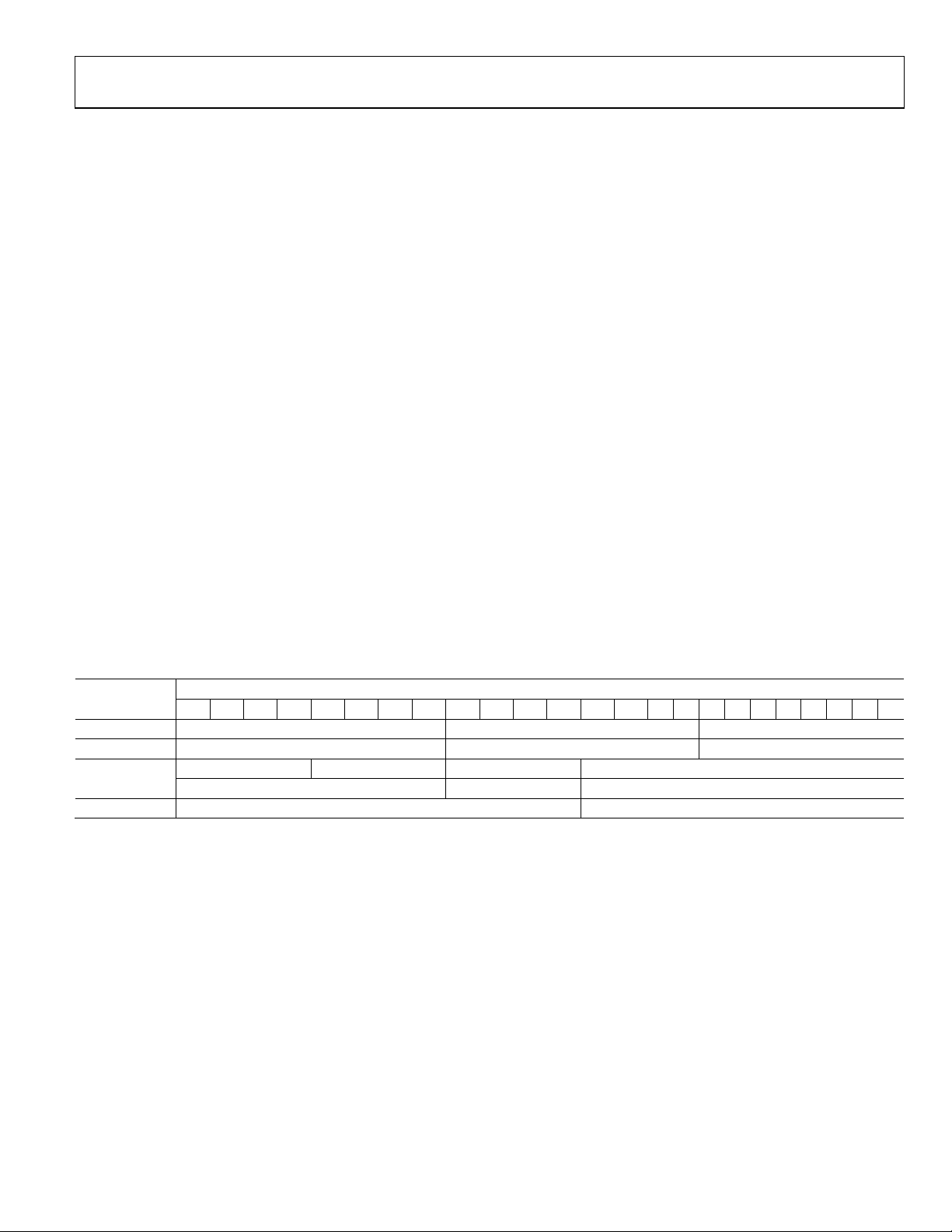
regenerated by dividing the 20-bit CTS value into the TMDS
clock, then multiplying by the 20-bit N value. This yields a
multiple of the sampling frequency of either 128 × f
f
. It is possible for this to be specified up to 1024 × fS.
S
SINK DEVICESOURCE DEVICE
128 ×
VIDEO
CLOCK
N
*N AND CTS VALUES ARE TRANSMITTED USING THE
AUDIO CLOCK REGENERATION PACKET. V IDEO
CLOCK IS T RANSM ITTED ON TMDS CLOCK CHANNEL .
DIVIDE
f
S
BY
REGISTER
CYCLE
TIME
COUNTER
N
N
Figure 5. N and CTS for Audio Clock
CTS*
TMDS
CLOCK
N*
÷ CTS × N
or 256 ×
S
128 ×
f
S
To provide the most flexibility in configuring the audio
sampling clock, an additional PLL is employed. The PLL
characteristics are determined by the loop filter design (see
Figure 6), the PLL charge pump current, and the VCO range
setting.
PV
C
8nF
C
P
1.5kΩ
FILT
Z
80nF
R
Z
DD
8043-008
Figure 6. PLL Loop Filter Detail
To fully support all audio modes for all video resolutions up
to 1080i, it is necessary to adjust certain audio-related registers
from their power-on default values. Ta b l e 7 describes these
registers and gives the recommended settings.
S
S
S
08043-007
Rev. 0 | Page 10 of 40
AD9393
AUDIO BOARD LEVEL MUTING
The audio can be muted through the infoframes or locally
via the serial bus registers. This can be controlled with
Register 0x57, Bits[7:6].
AVI Infoframes
The HDMI TMDS transmission contains infoframes with
specific information for the monitor such as:
• Audio information
• Two channels to eight channels of audio identified
• Audio coding
• Audio sampling frequency
• Speaker placement
• N and CTS values (for reconstruction of the audio)
• Muting
• Source information
• CD
• SACD
• DVD
• Video information
• Video ID code (per CEA861B)
• Color space
• Aspect ratio
• Horizontal and vertical bar information
• MPEG frame information (I, B, or P frame)
• Vendor (transmitter source) name and product model
This information is the fundamental difference between DVI
and HDMI transmissions and is located in the read-only registers
Register 0x5A to Register 0xEE. In addition to this information,
registers are provided to indicate that new information has been
received. Registers with addresses ending in 7 or F beginning
with Register 0x87 contain the new data flags (NDF)
information. All of these registers contain the same information
and all are reset when any of them are read. Although there is
no external interrupt signal, it is very easy for the user to read
any of the NDF registers to see if there is new information to be
processed.
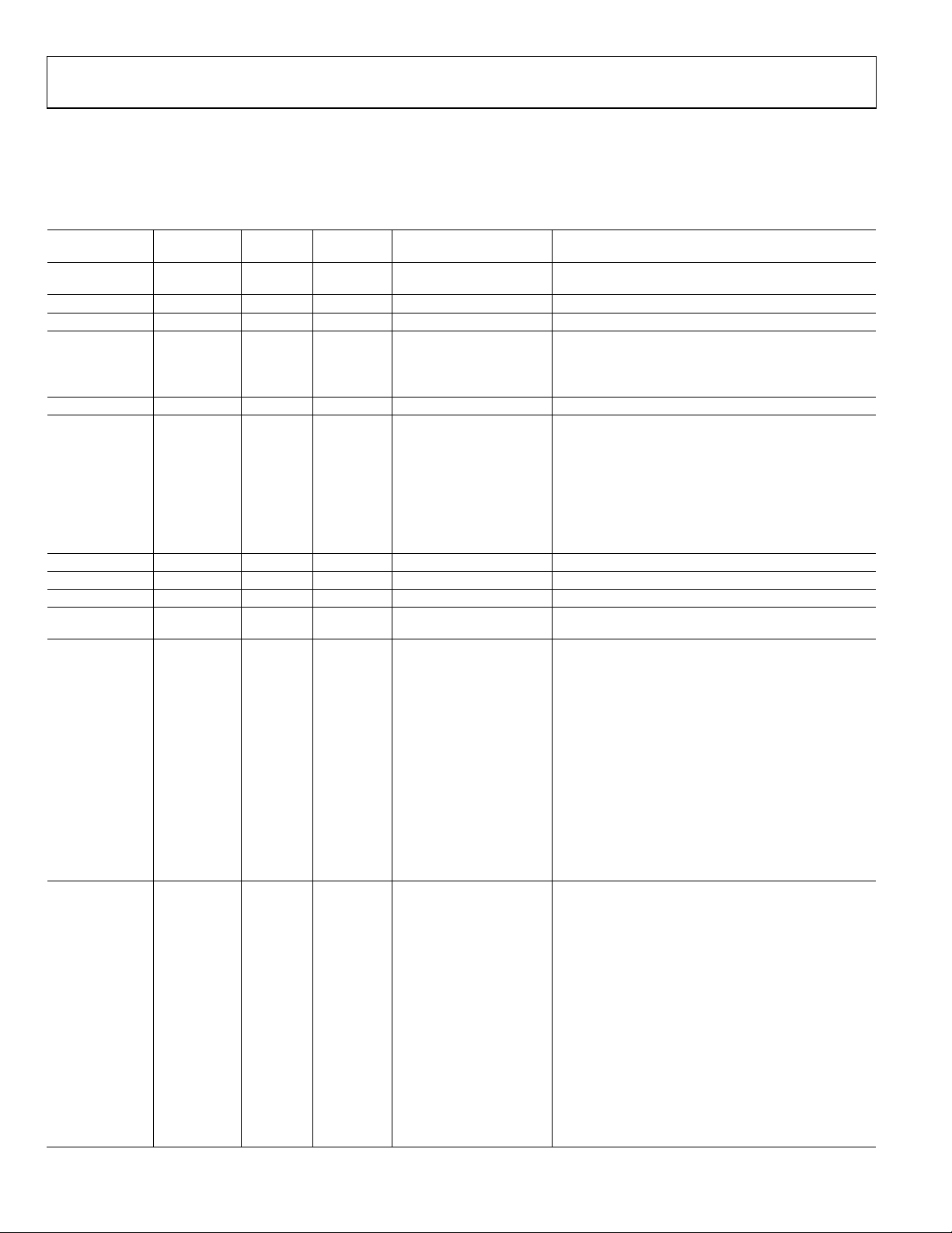
OUTPUT DATA FORMATS
The AD9393 supports 4:4:4, 4:2:2, double data-rate (DDR), and
BT656 output formats. Register 0x25[3:0] controls the output
mode. These modes and the pin mapping are illustrated in
Tabl e 8.
Table 8. Output Formats
Port
4:4:4 Red/Cr [7:0] Green/Y [7:0] Blue/Cb [7:0]
4:2:2 CbCr [7:0] Y [7:0]
4:4:4 DDR
4:2:2 to 12-bit CbCr [11:0] Y [11:0]
1
Arrows indicate clock edge. The rising edge of clock = ↑, the falling edge = ↓.
23 22 21 20 19 18 17 16 15 14 13 12 11 10 9 8 7 6 5 4 3 2 1 0
DDR
DDR ↓ R [7:0] DDR ↓ G [7:4] DDR 4:2:2 ↓ Y, Y [11:0]
1
Bits D[23:0]
↑ G [3:0] DDR ↑ B [7:4] DDR ↑ B [3:0] DDR 4:2:2 ↑ CbCr [11:0]
DDR 4:2:2
↑ CbCr ↓ Y, Y
Rev. 0 | Page 11 of 40
AD9393
2-WIRE SERIAL REGISTER MAP
The AD9393 is initialized and controlled by a set of registers that determines the operating modes. An external controller is employed to
write and read the control registers through the 2-wire serial interface port.
Table 9. Control Register Map
Default
Hex Address Read/Write Bits
0x00 Read [7:0] 00000000 Chip revision Chip revision ID. Revision is read [7:4] = major revision. [3:0]
0x01 Read/write [7:0] 01101001 PLL divider MSB PLL feedback divider value MSB.
0x02 Read/write [7:4] 1101xxxx PLL divider LSB PLL feedback divider value LSB.
0x03 Read/write [7:6] 01xxxxxx VCO range VCO range.
[5:3] xx001xxx Charge pump Charge pump current control for PLL.
[2] xxxxx0xx
0x11 Read/write [7:0] 00000000 Reserved Must be set to 0x00 (default).
0x12 Read/write [7] 1xxxxxxx Input HSYNC polarity 0 = active low.
1 = active high.
[6] x0xxxxxx HSYNC polarity override 0 = auto HSYNC polarity.
1 = manual HSYNC polarity.
[5] xx1xxxxx Input VSYNC polarity 0 = active low.
1 = active high.
[4] xxx0xxxx VSYNC polarity override 0 = auto VSYNC polarity.
1 = manual VSYNC polarity.
0x17 Read [3:0] xxxx0000 HSYNCs per VSYNC MSB MSB of HSYNCs per VSYNC.
0x18 Read [7:0] 00000000 HSYNCs per VSYNC LSB HSYNCs per VSYNC count.
0x22 Read/write [7:0] 4 VSYNC duration VSYNC duration.
0x23 Read/write [7:0] 32 HSYNC duration HSYNC duration. Sets the duration of the output HSYNC in
0x24 Read/write [7] 1xxxxxxx HSYNC output polarity Output HSYNC polarity.
0 = active low output.
1 = active high output.
[6] x1xxxxxx VSYNC output polarity Output VSYNC polarity.
0 = active low output.
1 = active high output.
[5] xx1xxxxx DE output polarity Output DE polarity.
0 = negative output.
1 = positive output.
[4] xxx1xxxx Field output polarity Output field polarity.
0 = active low output.
1 = active high output.
[0] xxxxxxx0 Output CLK invert 0 = noninverted clock output.
1 = inverted clock output.
0x25 Read/write [7:6] 01xxxxxx Output CLK select Selects which clock to use on output ball. 1× CLK is divided
00 = ½× CLK.
01 = 1× CLK.
10 = 2× CLK.
11 = 90° phase 1× CLK.
[5:4] xx11xxxx Output drive strength Sets the drive strength of the outputs. 00 = lowest, 11 =
[3:2] xxxx00xx Output mode Selects the data output mapping.
00 = 4:4:4 mode (normal).
01 = 4:2:2 + DDR 4:2:2 on D[7:0].
10 = DDR 4:4:4 + DDR 4:2:2 on D[7:0].
11 = 12-bit 4:2:2.
[1] xxxxxx1x Primary output enable Enables primary output.
[0] xxxxxxx0 Secondary output enable Enables secondary output (DDR 4:2:2 in Output Mode 1
Value
Register Name Description
= minor revision.
PLL enable
This bit enables a lower frequency to be used for audio
MCLK generation.
pixel clocks.
down from TMDS clock input when pixel repetition is in use.
highest.
and Output Mode 2).
Rev. 0 | Page 12 of 40
 Loading...