ANALOG DEVICES AD9389A Service Manual

现货库存、技术资料、百科信息、热点资讯,精彩尽在鼎好!
A
High Performance
FEATURES
General
Digital video
Digital audio
Special features for easy system design
TM
HDMI
/DVI transmitter compatible with HDMI v1.2a,
DVI v1.0, and HDCP 1.1
Internal key storage for HDCP
Single 1.8 V power supply
Video/audio inputs accept logic levels from 1.8 V to 3.3 V
64-lead LFCSP, Pb-free package
80 MHz operation supports all resolutions from 480i to
720p/1080i and XGA-75 Hz
Programmable two-way color space converter
Supports RGB, YCbCr, DDR
Supports ITU656 based embedded syncs
Auto input video format timing detection (CEA-861B)
Supports standard S/PDIF for stereo LPCM or compressed
audio up to 192 kHz
Supports 8-channel uncompressed LPCM I
2
S audio up to
192 kHz
On-chip MPU with I
2
C® master to perform HDCP
operations and EDID reading operations
5 V tolerant I
2
C and HPD I/Os, no extra device needed
No audio master clock needed for supporting
S/PDIF and I
2
S
On-chip MPU reports HDMI events through interrupts and
registers
CLK
VSYNC
HSYNC
D[23:0]
S/PDIF
MCLK
I2S[3:0]
LRCLK
SCLK
DE
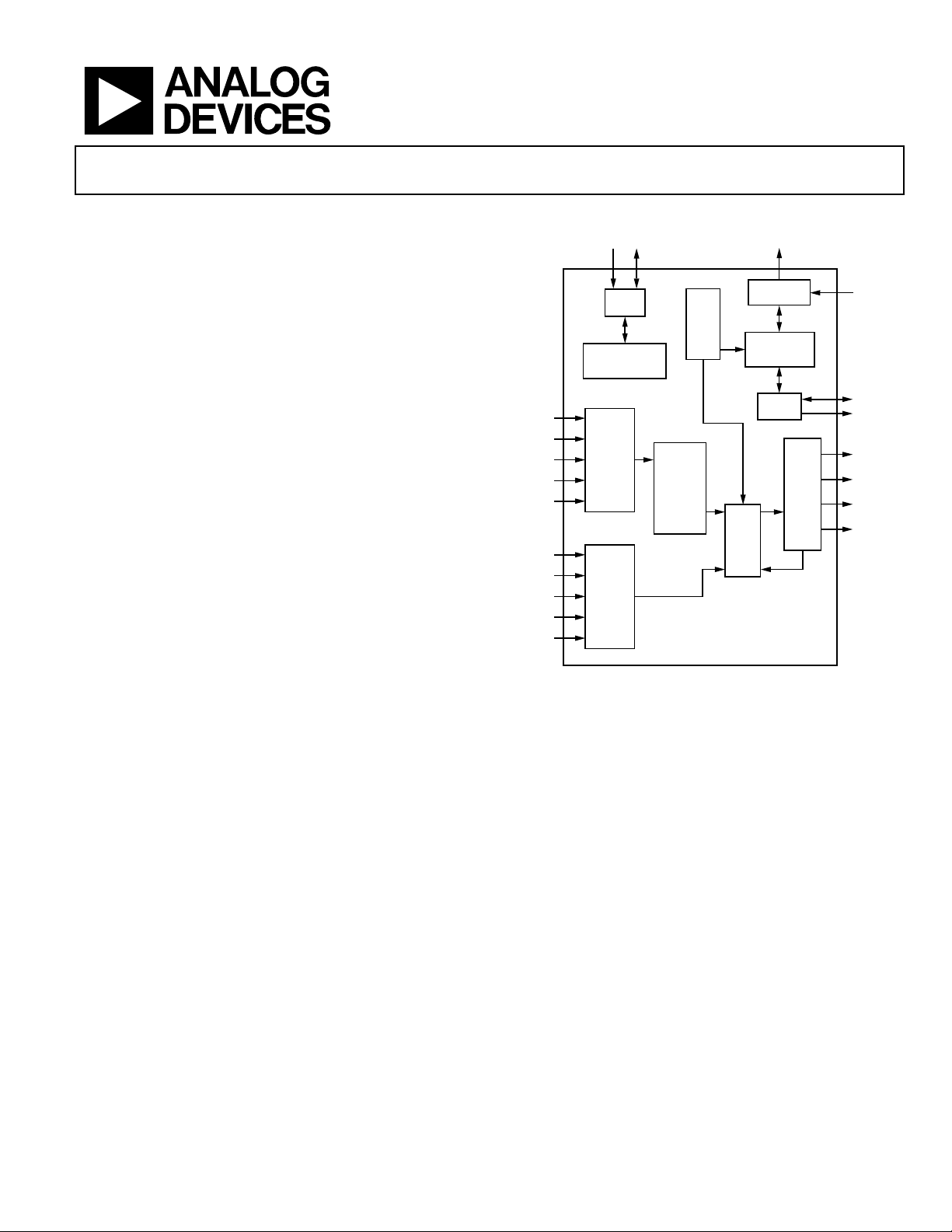
HDMI/DVI Transmitter
AD9389A
FUNCTIONAL BLOCK DIAGRAM
INTERRUPT
HANDLER
HDCP-EDID
MICRO-
CONTROLLER
MASTER
XOR
MASK
AD9389A
INT
I2C
HDMI
Tx
CORE
SD
SCL
I2C
SLAVE
REGISTER
CONFIGURATION
LOGIC
VIDEO
DATA
CAPTURE
AUDIO
DATA
CAPTURE
COLOR
SPACE
CONVER-
SION
4:2:2 TO
4:4:4
CONVER-
SION
Figure 1.
HDCP
CORE
HPD
DDCSDA
DDCSCL
Tx0[1:0]
Tx1[1:0]
Tx2[1:0]
TxC[1:0]
06187-001
APPLICATIONS
DVD players and recorders
Digital set-top boxes
A/V receivers
Digital cameras and camcorders
HDMI repeater/splitter
GENERAL DESCRIPTION
The AD9389A-BBCZ is an 80 MHz, high definition multimedia
interface (HDMI) v.1.2a transmitter. It supports HDTV formats
up to 720p/1080i, and computer graphic resolutions up to XGA
(1024 × 768 @ 75 Hz). With the inclusion of HDCP, the AD9389A
allows the secure transmission of protected content as specified
by the HDCP v1.1 protocol.
2
The AD9389A supports both S/PDIF and 8-channel I
2
Its high fidelity 8-channel I
S can transmit either stereo or 7.1
surround audio at 192 kHz. The S/PDIF can carry stereo LPCM
Rev. 0
Information furnished by Analog Devices is believed to be accurate and reliable. However, no
responsibility is assumed by Anal og Devices for its use, nor for any infringements of patents or ot her
rights of third parties that may result from its use. Specifications subject to change without notice. No
license is granted by implication or otherwise under any patent or patent rights of Analog Devices.
Trademarks and registered trademarks are the property of their respective owners.
S audio.
audio or compressed audio including Dolby® Digital, DTS®,
and THX®.
The AD9389A helps to reduce system design complexity and
cost by incorporating such features as an internal MPU for
2
HDCP operations, an I
1.8 V power supply and 5 V tolerance on I
C master for EDID reading, a single
2
C and hot plug
detect pins.
Fabricated in an advanced CMOS process, the AD9389A is
available in a space saving, 64-lead LFCSP surface-mount
package. The LFCSP package is specified from 0°C to 70°C.
One Technology Way, P.O. Box 9106, Norwood, MA 02062-9106, U.S.A.
Tel: 781.329.4700 www.analog.com
Fax: 781.461.3113 ©2006 Analog Devices, Inc. All rights reserved.

AD9389A
TABLE OF CONTENTS
Features .............................................................................................. 1
Applications........................................................................................7
Applications....................................................................................... 1
Functional Block Diagram .............................................................. 1
General Description......................................................................... 1
Revision History ............................................................................... 2
Specifications..................................................................................... 3
Absolute Maximum Ratings............................................................ 4
Explanation of Test Levels........................................................... 4
ESD Caution.................................................................................. 4
Pin Configuration and Function Descriptions............................. 5
REVISION HISTORY
10/06—Revision 0: Initial Version
Design Resources ..........................................................................7
Document Conventions ...............................................................7
PCB Layout Recommendations.......................................................8
Power Supply Bypassing ...............................................................8
Digital Inputs .................................................................................8
External Swing Resistor................................................................8
Output Signals ...............................................................................8
Outline Dimensions ..........................................................................9
Ordering Guide .............................................................................9
Rev. 0 | Page 2 of 12

AD9389A
SPECIFICATIONS
Table 1.
Te st
Parameter Conditions Temp
DIGITAL INPUTS
Input Voltage, High (VIH) Full VI 1.4 V
Input Voltage, Low (VIL) Full VI 0.7 V
Input Capacitance 25°C V 3 pF
DIGITAL OUTPUTS
Output Voltage, High (VOH) Full VI VDD − 0.1 V
Output Voltage, Low (VOL) Full VI 0.4 V
THERMAL CHARACTERISTICS
Thermal Resistance
θJC Junction-to-Case V 15.2 °C/W
θJA Junction-to-Ambient V 59 °C/W
Ambient Temperature Full V −25 +25 +90 °C
DC SPECIFICATIONS
Input Leakage Current, I
IL
25°C VI −10 +10 μA
Input Clamp Voltage −16 mA 25°C V −0.8 V
+16 mA 25°C V +0.8 V
Differential High Level Output Voltage V AVCC V
Differential Output Short-Circuit Current IV 10 μA
POWER SUPPLY
VDD (All) Supply Voltage Full IV 1.71 1.8 1.89 V
VDD Supply Voltage Noise Full V 50 mV p-p
Power-Down Current With active video applied 25°C IV 9 mA
Transmitter Supply Current
2
80 MHz, typical random
25°C IV 143 155 mA
pattern
Transmitter Total Power Full VI 257 280 mW
AC SPECIFICATIONS
CLK Frequency 25°C IV 13.5 80 MHz
TMDS Output CLK Duty Cycle 25°C IV 48 52 %
Worst Case CLK Input Jitter Full IV 2 ns
Input Data Setup Time Full IV 1 ns
Input Data Hold Time Full IV 1 ns
TMDS Differential Swing VI 800 1000 1200 mV
V
SYNC
and H
Delay from DE Falling
SYNC
VI 1 UI
Edge
V
SYNC
and H
Delay to DE Rising Edge VI 1 UI
SYNC
DE High Time 25°C VI 8191 UI
DE Low Time 25°C VI 138 UI
Differential Output Swing
Low-to-High Transition Time 25°C VII 75 490 ps
High-to-Low Transition Time 25°C VII 75 490 ps
AUDIO AC TIMING
Sample Rate I2S and S/PDIF Full IV 32 192 kHz
I2S Cycle Time 25°C IV 1 UI
I2S Setup Time 25°C IV 15 ns
I2S Hold Time 25°C IV 0 ns
Audio Pipeline Delay 25°C IV 75 μs
1
See the Explanation of Test Levels section.
2
Using low output drive strength.
3
UI = unit interval.
Rev. 0 | Page 3 of 12
Level
1
Min Typ Max Unit
3

AD9389A
ABSOLUTE MAXIMUM RATINGS
Table 2.
Parameter Rating
Digital Inputs 5 V to 0.0 V
Digital Output Current 20 mA
Operating Temperature Range 0°C to +70°C
Storage Temperature Range −65°C to +150°C
Maximum Junction Temperature 150°C
Maximum Case Temperature 150°C
Stresses above those listed under Absolute Maximum Ratings
may cause permanent damage to the device. This is a stress
rating only; functional operation of the device at these or any
other conditions above those indicated in the operational
section of this specification is not implied. Exposure to absolute
maximum rating conditions for extended periods may affect
device reliability.
EXPLANATION OF TEST LEVELS
I. 100% production tested.
II. 100% production tested at 25°C and sample tested at
III. Sample tested only.
IV. Parameter is guaranteed by design and characterization
V. Parameter is a typical value only.
VI. 100% production tested at 25°C; guaranteed by design
VII. Limits defined by HDMI specification; guaranteed by
ESD CAUTION
specified temperatures.
testing.
and characterization testing.
design and characterization testing.
Rev. 0 | Page 4 of 12
 Loading...