

现货库存、技术资料、百科信息、热点资讯,精彩尽在鼎好!
2.3MHz Typical at Nominal Conditions, 2VFS Int Ref
Rev. PrJ
6/25/2004
Quad 8-Bit, 65 MSPS
Serial LVDS 3V A/D Converter
Preliminary Technical Data AD9289
FEATURES
• Four ADCs in one package
• Serial LVDS digital output data rates up to 520 Mbps (ANSI-
644)
• Data clock output provided
• SNR = 47 dB (to Nyquist)
• Excellent Linearity:
DNL = ±0.25 LSB (Typical)
INL = ±0.5 LSB (Typical)
• 400 MHz full power analog bandwidth
• Power dissipation = 112 mW Core ADC Power
per channel at 65 MSPS
• 1 Vpp – 2 Vpp input voltage range
• +3.0 V supply operation
• Power down mode
APPLICATIONS
• Tape drives
• Medical imaging
PRODUCT DESCRIPTION
The AD9289 is a quad 8-bit, 65 MSPS analog–to–digital converter
with an on–chip track–and–hold circuit and is designed for low
cost, low power, small size and ease of use. The product operates
up to 65 MSPS conversion rate and is optimized for outstanding
dynamic performance where a small package size is critical.
The ADC requires a single+3V power supply and an LVDS
compatible sample rate clock for full performance operation. No
external reference or driver components are required for many
applications. A separate output power supply pin supports LVDS
compatible serial digital output levels.
The ADC automatically multiplies up the sample rate clock for the
appropriate LVDS serial data rate. An FCO trigger is provided to
signal a new output byte. Power down is supported, and the ADC
consumes less than 10mW when enabled.
Fabricated on an advanced CMOS process, the AD9289 is
available in a 64-ball mini-BGA package (64 CSP_BGA)
specified over the industrial temperature range (–40°C to +85°C).
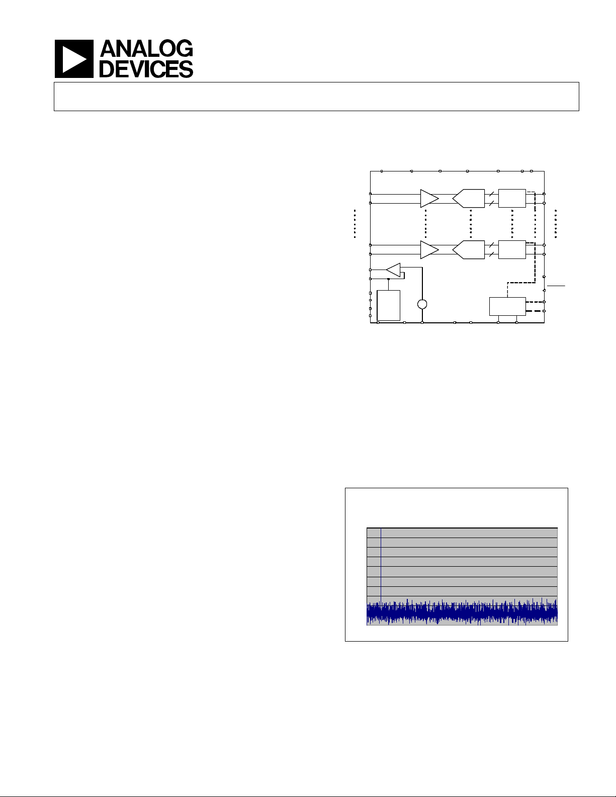
FUNCTIONAL BLOCK DIAGRAM
VIN+A
VIN-A
VIN+D
VIN-D
VREF
SENSE
REFT_A
REFB_A
REFT_B
REFB_B
SHARED_REF CML
AVDD DRVDD
DRGND
Ref
Select
Figure 1. Functional Block Diagram
PDWN
AD9289
SHA
SHA
+
0.5 V
-
Pipeline
ADC
Pipeline
ADC
FCO+ FCO-
8
8
Data Rate
Multiplier
CLK+ CLK-AGND
Serial
LVDS
Serial
LVDS
OR+ OR-S1
PRODUCT HIGHLIGHTS
1. Four analog-to-digital converters are contained in one small,
space saving package.
2. A Data Clock Out (DCO) is provided which operates up to
260 MHz.
3. The outputs of each ADC are serialized and provided on the
rising and falling edge of DCO). Output data rates up to 520
Mbps (8 bits x 65 MSPS) are available.
4. The AD9289 operates from a single 3V power supply.
5. The clock duty cycle stabilizer maintains performance over a
wide range of input clock duty cycles
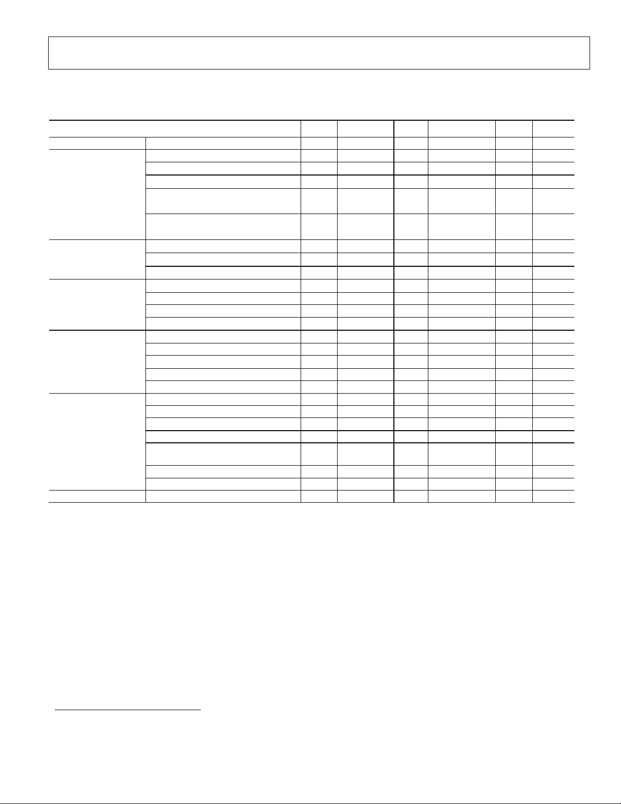
AD9289 R1
SNR = 49.1dB, SFDR = 71.9dB
0
-10
-20
-30
-40
-50
-60
-70
-80
-90
-100
0 5 10 15 20 25 30
D1+A
D1-A
D1+D
D1-D
LVDSBIAS
LOCK
DCO+
DCO-
Information furnished by Analog Devices is believed to be accurate and
reliable. However, no responsibility is assumed by Analog Devices for its
use, nor for any infringements of patents or other rights of third parties
that may result from its use. No license is granted by implication or
otherwise under any patent or patent rights of Analog Devices. Trademarks
and registered trademarks are the property of their respective companies.
Figure 2. Measured FFT
One Technology Way, P.O. Box 9106, Norwood, MA 02062-9106,
U.S.A.
Tel: 781.329.4700 www.analog.com
Fax: 781.326.8703 © 2004 Analog Devices, Inc. All rights reserved.

AD9289 Preliminary Technical Data
TABLE OF CONTENTS
AD9289—Specifications ............................................................ 3
DIGITAL SPECIFICATIONS ................................................. 4
AC SPECIFICATIONS........................................................... 4
SWITCHING SPECIFICATIONS........................................... 5
EXPLANATION OF TEST LEVELS...................................... 5
Absolute Maximum Ratings........................................................ 6
Definitions .................................................................................7
Theory of Operation ...................................................................9
Clock Input............................................................................. 9
Analog Inputs......................................................................... 9
Voltage Reference....................................................................9
Internal Reference Connection ...............................................10
External Reference Operation ................................................10
Digital Outputs......................................................................11
Timing..................................................................................11
PLL
CML Pin ............................................................................... 11
Overange............................................................................... 11
Pin Configurations ....................................................................13
Timing Diagram........................................................................14
Ordering Guide .....................................................................16
Output ................................................................ 11
LOCK
REVISION HISTORY
Revision PrA: Initial Version
Revision PrB: Updated specifications
Revision PrC: Added application section
Revision PrD: Revised block diagram, added LOCK/ output to timing diagram, added offset and gain matching definitions, updated Theory of
Operation
Revision PrE: Updated timing diagram and PLL description
Revision PrF: Updated Timing Specs, Pin Function Description (Added DNC pins), Added Pin Configuration Diagram and Package Outline
Revision PrG: Added DCR pin info, updated lvdsbias resistor value,
Revision H: Updated reference description, Removed S3, Added scope plot, Added FFT, Updated Tpd, Tcpd, Tmsb, Power, Updated
LVDSBIAS Resistor value, Min Encodeà 20MSPS
Revision I: Updated Power Supply Range, Added thermal impedance number,
Revision J: Added CML description, Modified Timing Diagram, Changed MSB naming to FCO,Removed S2, Modified Tpd,
Rev. PrJ | Page 2 of 16 6/25/2004
Preliminary Technical Data AD9289
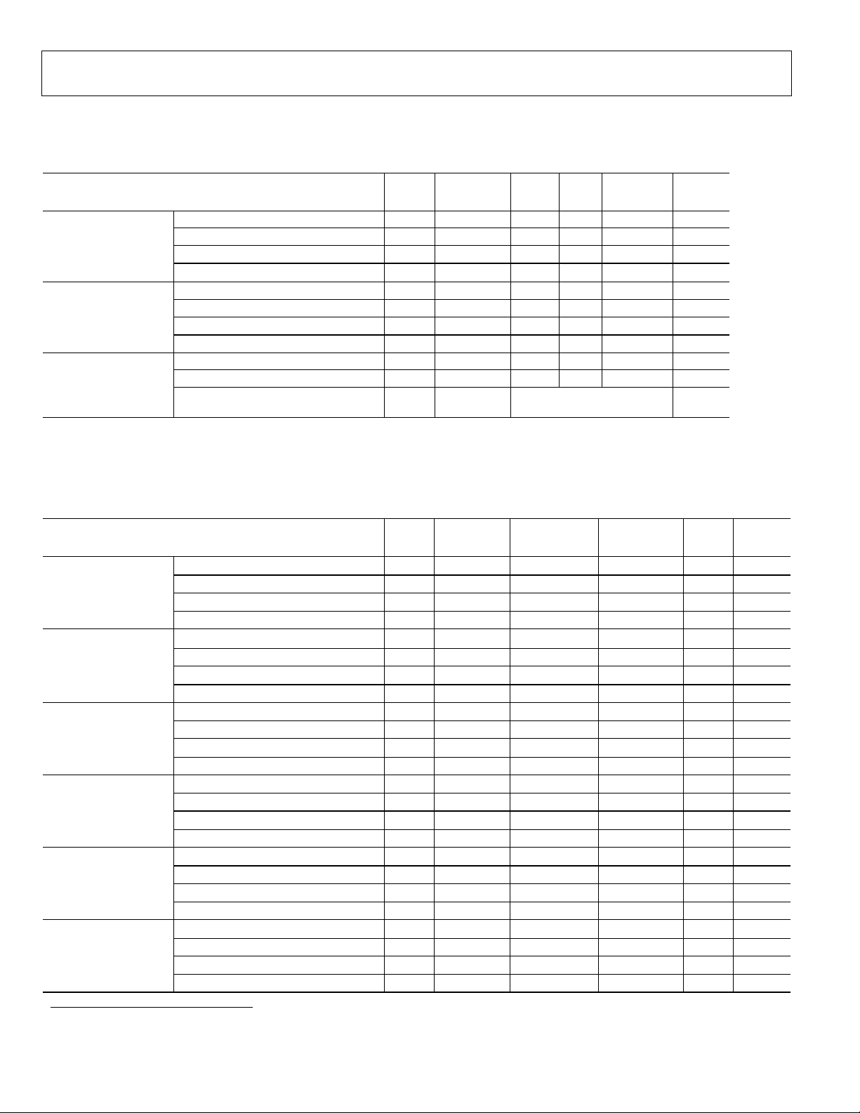
AD9289—SPECIFICATIONS
AVDD = 3.0V, DRVDD = 3.0V; INT REF; DIFFERENTIAL ANALOG AND CLOCK INPUTS
Parameter Temp Test Level Min Typ Max Unit
RESOLUTION 8 Bits
No Missing Codes Full VI Guaranteed
Offset Matching
Gain Matching2
ACCURACY
TEMPERATURE
DRIFT
REFERENCE
ANALOG INPUTS
POWER SUPPLY
CROSSTALK Crosstalk Full V 70 dB
Differential Nonlinearity (DNL)
Full VI LSB
Integral Nonlinearity (INL)
Full VI LSB
Offset Error Full V
Gain Error2 Full V
Reference Full V
Internal Reference Voltage
Output Current Full V uA
Input Current Full V uA
Input Resistance Full V 7
Differential Input Voltage Range 1 –2 Vpp
Common Mode Voltage Full V 1.5 V
Input Resistance Full V tbd
Input Capacitance Full V 5 pF
Analog Bandwidth, Full Power Full V 400 MHz
AVDD Full IV 2.85 3.0 3.15 V
DRVDD Full IV 2.85 3.0 3.15 V
Power Dissipation3 Full VI 558 mW
Power Down Dissipation Full VI <10 mW
Power Supply Rejection Ratio
(PSRR)
IAVDD3 Full VI 150 mA
DRVDD3 Full VI 36 mA
1
25°C
25°C
25°C
25°C
25°C
25°C
Table 1
I
I
I
I
± 25
± 2
± 0.25
± 0.5
± 16
± 150
I 0.5 V
I mV/V
mV
% FS
LSB
LSB
ppm/°C
ppm/°C
ppm/°C
kΩ
kΩ
1
Specifications subject to change without notice
2
Gain error and gain temperature coefficients are based on the ADC only (with a fixed 0.5 V external reference and a 1 V p-p differential analog input).
3
Power dissipation measured with rated encode and a dc analog input (Outputs Static, I
0.5dBFS.
Rev. PrJ | Page 3 of 16 6/25/2004
VDD
= 0.). I
VCC
and I
measured with TBD MHz analog input @
VDD
AD9289 Preliminary Technical Data
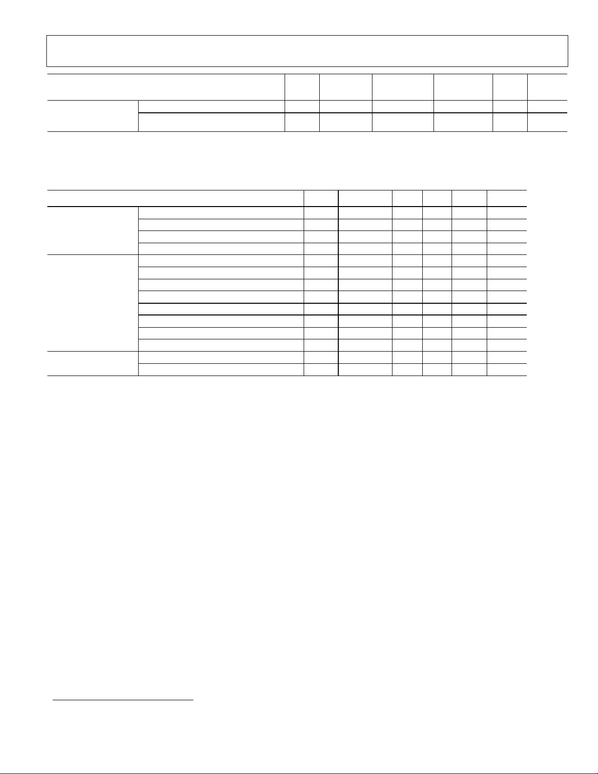
DIGITAL SPECIFICATIONS
AVDD = 3.0V, DRVDD = 3.0V
Parameter Temp Test
Min Typ Max Unit
Level
Differential Input Voltage1 Full IV 247 mVpp
CLOCK INPUTS
(CLK+, CLK-)
LOGIC INPUTS
(LVDS Mode)
Input Common Mode Voltage Full IV 1.25 V
Input Resistance Full IV
Input Capacitance
Logic ‘1’ Voltage Full IV 2.0 V
Logic ‘0’ Voltage Full IV 0.8 V
Input Resistance Full IV 30
Input Capacitance Full IV 4 PF
Differential Output Voltage (VOD) Full IV 247 454 mV
Output Offset Voltage (VOS) Full IV 1.125 1.375 V DIGITAL OUTPUTS
Output Coding Full IV Twos Complement or
Table 2: Digital Specifications
25°C
IV pF
Binary
kΩ
kΩ
AC SPECIFICATIONS2
AVDD = 3.0 V, DRVDD = 3.0 V; INTERNAL REF; DIFFERENTIAL ANALOG AND CLOCK INPUT, LVDS OUTPUT
MODE
Parameter Temp Test
Level
SIGNAL TO NOISE
RATIO (SNR) –
Without Harmonics
SIGNAL TO NOISE
RATIO (SINAD) –
With Harmonics
EFFECTIVE
NUMBER OF BITS
(ENOB)
SPURIOUS FREE
DYNAMIC RANGE
(SFDR)
SECOND AND
THIRD HARMONIC
DISTORTION
TOTAL HARMONIC
DISTORTION (THD)
1
Clock Inputs are LVDS compatible .Clock Inputs require external DC bias and cannot be AC coupled.
2
SNR/harmonics based on an analog input voltage of –0.5 dBFS referenced to a 1 Vpp full-scale input range.
fIN= 10.3 MHz
fIN= 19.6 MHz
fIN= 32.5 MHz
fIN= 51 MHz
fIN= 10.3 MHz
fIN= 19.6 MHz
fIN= 32.5 MHz
fIN= 51 MHz
fIN= 10.3 MHz
fIN= 19.6 MHz
fIN= 32.5 MHz
fIN= 51 MHz
fIN= 10.3 MHz
fIN= 19.6 MHz
fIN= 32.5 MHz
fIN= 51 MHz
fIN= 10.3 MHz
fIN= 19.6 MHz
fIN= 32.5 MHz
fIN= 51 MHz
fIN= 10.3 MHz
fIN= 19.6 MHz
fIN= 32.5 MHz
fIN= 51 MHz
25°C
25°C
25°C
25°C
25°C
25°C
25°C
25°C
25°C
25°C
25°C
25°C
25°C
25°C
25°C
25°C
25°C
25°C
25°C
25°C
25°C
25°C
25°C
25°C
V 47.5 dB
V dB
I 47.5 dB
V dB
V 47 dB
V dB
I 47 dB
V dB
V 7.5 Bits
V Bits
I 7.5 Bits
V Bits
V 62 dB
V dB
I 59 dB
V dB
V 62 dBc
V dBc
I 59 dBc
V dBc
V 60 dBc
V dBc
I 58 dBc
V dBc
Min Typ Max Unit
Rev. PrJ | Page 4 of 16 6/25/2004
Preliminary Technical Data AD9289
Parameter Temp Test
Level
f
INTERMOD
DISTORTION (IMD)
= 19 MHz, f
IN1
f
= xx MHz, f
IN1
= 20 MHz
IN2
= xx MHz
IN2
25°C
25°C
Table 3: AC Specifications
V dBc TWO TONE
V dBc
SWITCHING SPECIFICATIONS
AVDD = 3.0 V, DRVDD = 3.0 V; DIFFERENTIAL ENCODE INPUT
Parameter Temp Test Level Min Typ Max Unit
Maximum Clock Rate Full VI 65 MSPS
CLOCK
OUTPUT
PARAMETERS IN
LVDS MODE
APERTURE
Minimum Clock Rate Full VI 20 MSPS
Clock Pulse Width High (tEH) Full IV 6.9 ns
Clock Pulse Width Low (tEL) Full IV 6.9 ns
Valid Time (tV)1 Full VI ns
Propagation Delay (tPD) 1 Full VI 10 ns
MSB Propagation Delay (t
) 1 Full VI 10 ns
MSB
Rise Time (tR) (20% to 80%) Full V 0.5 ns
Fall Time (tF) (20% to 80%) Full V 0.5 ns
DCO Propagation Delay (t
Data to DCO Skew (tPD – t
) Full VI 10 ns
CPD
) Full IV
CPD
Pipeline Latency Full VI 6 cycles
Aperture Delay (tA)
Aperture Uncertainty (Jitter)
Table 4: Switching Specifications
25°C
25°C
Min Typ Max Unit
+/- 100
pS
V ps
V <1 ps rms
EXPLANATION OF TEST LEVELS
TEST LEVEL
I 100% production tested.
II 100% production tested at +25°C and guaranteed by design and characterization at specified temperatures.
III Sample Tested Only
IV Parameter is guaranteed by design and characterization testing.
V Parameter is a typical value only.
VI 100% production tested at +25°C and guaranteed by design and characterization for industrial temperature range.
1
tV and t
not to exceed an ac load of 5 pF or a dc current of ±40 µA. Rise and fall times measured from 20% to 80%.
are measured from the transition points of the CLK input to the 50%/50% levels of the digital outputs swing. The digital output load during test is
PD
Rev. PrJ | Page 5 of 16 6/25/2004

AD9289 Preliminary Technical Data
ABSOLUTE MAXIMUM RATINGS
Parameter Rating
AVDD Voltage
DRVDD Voltage
Analog Input Voltage
Electrical
Environmental
Thermal Impedance1
Stresses above those listed under the Absolute Maximum Ratings may cause permanent damage to the device. This is a stress rating only;
functional operation of the device at these or any other conditions above those indicated in the operational section of this specification is not
implied. Exposure to absolute maximum rating conditions for extended periods may affect device reliability.
Analog Input Current
Digital Input Voltage
Digital Output Current
VREF Input Voltage
Operating Temperature Range (Ambient)
Maximum Junction Temperature
Lead Temperature (Soldering, 10 sec)
Maximum Case Temperature
Storage Temperature Range (Ambient)
Table 5: Absolute Maximum Ratings
-40°C to +85°C
40°C/W
1
θ
for a 4 layer PCB with solid ground plane in still air.
ja
Rev. PrJ | Page 6 of 16 6/25/2004

Preliminary Technical Data AD9289
02.6
−
−
DEFINITIONS
pulse (CLK+) should be left in logic “1” state to achieve rated
ANALOG BANDWIDTH
The analog input frequency at which the spectral power of the
fundamental frequency (as determined by the FFT analysis) is
reduced by 3 dB.
performance; pulse width low is the minimum time the clock pulse
should be left in low state. See timing implications of changing t
in text. At a given clock rate, these specs define an acceptable
clock duty cycle.
clk
APERTURE DELAY
The delay between the 50% point of the rising edge of the
ENCODE command and the instant at which the analog input is
sampled.
APERTURE UNCERTAINTY (JITTER)
The sample-to-sample variation in aperture delay.
CROSSTALK
Coupling onto one channel being driven by a low level (-40 dBFS)
signal when the adjacent interfering channel is driven by a fullscale signal.
DIFFERENTIAL ANALOG INPUT RESISTANCE,
DIFFERENTIAL ANALOG INPUT CAPACITANCE,
AND DIFFERENTIAL ANALOG INPUT IMPEDANCE
The real and complex impedances measured at each analog input
port. The resistance is measured statically and the capacitance and
differential input impedances are measured with a network
analyzer.
DIFFERENTIAL ANALOG INPUT VOLTAGE RANGE
The peak to peak differential voltage that must be applied to the
converter to generate a full scale response. Peak differential
voltage is computed by observing the voltage on a single pin and
subtracting the voltage from the other pin, which is 180 degrees
out of phase. Peak to peak differential is computed by rotating the
inputs phase 180 degrees and taking the peak measurement again.
Then the difference is computed between both peak measurements.
DIFFERENTIAL NONLINEARITY
The deviation of any code width from an ideal 1 LSB step.
FULL SCALE INPUT POWER
Expressed in dBm. Computed using the following equation:
Power
Fullscale
2
V
Fullscale
=
log10
Z
001.
Input
rms
GAIN ERROR
Gain error is the difference between the measured and ideal full
scale input voltage range of the worst ADC.
GAIN MATCHING
Expressed in %FSR. Computed using the following equation:
minmax
=
ngGainMatchi
where FSR
FSR
min
is the most positive gain error of the ADCs and
max
is the most negative gain error of the ADCs.
+
2
FSRFSR
minmax
FSRFSR
%100*
HARMONIC DISTORTION, SECOND
The ratio of the rms signal amplitude to the rms value of the
second harmonic component, reported in dBc.
HARMONIC DISTORTION, THIRD
The ratio of the rms signal amplitude to the rms value of the third
harmonic component, reported in dBc.
EFFECTIVE NUMBER OF BITS
The effective number of bits (ENOB) is calculated from the
measured SNR based on the equation:
ENOB
=
MEASURED
76.1 dBSNR
INTEGRAL NONLINEARITY
The deviation of the transfer function from a reference line
measured in fractions of 1 LSB using a “best straight line”
determined by a least square curve fit.
MINIMUM CONVERSION RATE
The encode rate at which the SNR of the lowest analog signal
frequency drops by no more than 3 dB below the guaranteed limit.
CLOCK PULSE WIDTH/DUTY CYCLE
Pulse width high is the minimum amount of time that the Clock
Rev. PrJ | Page 7 of 16 6/25/2004

AD9289 Preliminary Technical Data
−
=
MAXIMUM CONVERSION RATE
The encode rate at which parametric testing is performed.
OFFSET ERROR
Offset error is the difference between the measured and ideal
voltage at the analog input that produces the midscale code at the
outputs. Offset error is given for the worst ADC.
OFFSET MATCHING
Expressed in mV. Computed using the following equation:
minmax OFFOFFhingOffsetMatc
where OFF
most negative offset error.
is the most positive offset error and OFF
max
min
is the
OUTPUT PROPAGATION DELAY
The delay between a differential crossing of CLK+ and CLK- and
the time when all output data bits are within valid logic levels.
NOISE (FOR ANY RANGE WITHIN THE ADC)
−−
noise
=
ZV
10*001.*
10
SignalSNRFS
dBFSdBcdBm
SIGNAL-TO-NOISE RATIO (WITHOUT
HARMONICS)
The ratio of the rms signal amplitude (set at 1 dB below full scale)
to the rms value of the sum of all other spectral components,
excluding the first five harmonics and dc.
SPURIOUS-FREE DYNAMIC RANGE (SFDR)
The ratio of the rms signal amplitude to the rms value of the peak
spurious spectral component. The peak spurious component may
or may not be a harmonic. It also may be reported in dBc (i.e.,
degrades as signal level is lowered) or dBFS (i.e., always related
back to converter full scale).
TWO-TONE INTERMODULATION DISTORTION
REJECTION
The ratio of the rms value of either input tone to the rms value of
the worst third order intermodulation product; reported in dBc.
TWO-TONE SFDR
The ratio of the rms value of either input tone to the rms value of
the peak spurious component. The peak spurious component may
or may not be an IMD product. It also may be reported in dBc (i.e.,
degrades as signal level is lowered) or in dBFS (i.e., always relates
back to converter full scale).
WORST OTHER SPUR
Where Z is the input impedance, FS is the full scale of the device
for the frequency in question, SNR is the value for the particular
input level and Signal is the signal level within the ADC reported
in dB below full scale. This value includes both thermal and
quantization noise.
POWER SUPPLY REJECTION RATIO
The ratio of a change in input offset voltage to a change in power
supply voltage.
SIGNAL-TO-NOISE-AND-DISTORTION (SINAD)
The ratio of the rms signal amplitude (set 1 dB below full scale) to
the rms value of the sum of all other spectral components,
including harmonics but excluding dc.
The ratio of the rms signal amplitude to the rms value of the worst
spurious component (excluding the second and third harmonic)
reported in dBc.
TRANSIENT RESPONSE TIME
Transient response time is defined as the time it takes for the ADC
to reacquire the analog input after a transient from 10% above
negative full scale to 10% below positive full scale.
OUT-OF-RANGE RECOVERY TIME
Out of range recovery time is the time it takes for the ADC to
reacquire the analog input after a transient from 10% above
positive full scale to 10% above negative full scale, or from 10%
below negative full scale to 10% below positive full scale.
Rev. PrJ | Page 8 of 16 6/25/2004

Preliminary Technical Data AD9289
THEORY OF OPERATION
Each A/D converter in the AD9289 architecture consists of a frontend sample and hold amplifier (SHA) followed by a pipelined
switched capacitor A/D converter. The pipelined A/D converter is
divided into two sections, consisting of six 1.5-bit stages and a
final 3-bit flash. Each stage provides sufficient overlap to correct
for flash errors in the preceding stages. The quantized outputs from
each stage are combined into a final 8-bit result in the digital
correction logic. The pipelined architecture permits the first stage
to operate on a new input sample while the remaining stages
operate on preceding samples. Sampling occurs on the rising edge
of the clock.
output driver supplies to avoid modulating the clock signal with
digital noise. Low jitter, crystal-controlled oscillators make the
best clock sources. If the clock is generated from another type of
source (by gating, dividing, or other methods), it should be retimed
by the original clock at the last step.
Analog Inputs
For best dynamic performance, the source impedances driving
VIN+ and VIN– should be matched such that common-mode
settling errors are symmetrical. These errors will be reduced by the
common-mode rejection of the A/D.
Each stage of the pipeline, excluding the last, consists of a low
resolution flash A/D connected to a switched capacitor DAC and
interstage residue amplifier (MDAC). The residue amplifier
magnifies the difference between the reconstructed DAC output
and the flash input for the next stage in the pipeline. One bit of
redundancy is used in each one of the stages to facilitate digital
correction of flash errors. The last stage simply consists of a flash
A/D.
The input stage contains a differential SHA that can be configured
as ac- or dc-coupled in differential or single-ended modes. The
output-staging block aligns the data, carries out the error correction
and passes the data to the output buffers.During power-down the
output buffers go into a high-impedance state.
Clock Input
Typical high-speed A/D converters use both clock edges to
generate a variety of internal timing signals, and as a result may be
sensitive to clock duty cycle. Commonly a +/-5% tolerance is
required on the clock duty cycle to maintain dynamic performance
characteristics. The AD9289 contains a clock duty cycle stabilizer
that retimes the non-sampling edge, providing an internal clock
signal with a nominal 50% duty cycle. This allows a wide range of
clock input duty cycles without affecting the performance of the
AD9289. As shown in TPC XX, noise and distortion performance
are nearly flat over at least a +/-15% range of duty cycle. The
stabilizer circuit can be bypassed by grounding input pin DCR. (
There is an internal 22K ohm pull-up resistor)
The duty cycle stabilizer uses a delay-locked loop (DLL) to create
the non-sampling edge. As a result, any changes to the sampling
frequency will require approximately 100 clock cycles to allow the
DLL to acquire and lock to the new rate. High-speed, highresolution A/Ds are sensitive to the quality of the clock input. The
degradation in SNR at a given full-scale input frequency (fA) due
only to aperture jitter (tA) can be calculated with the following
equation:
SNR degradation = 20 × log10 [1/2 × pi × fA ×
tA]
In the equation, the rms aperture jitter, tA, represents the root sum
square of all jitter sources, which include the clock input, analog
input signal, and A/D aperture jitter specification. Undersampling
applications are particularly sensitive to jitter.
The clock input should be treated as an analog signal in cases
where aperture jitter may affect the dynamic range of the AD9289.
Power supplies for clock drivers should be separated from the A/D
Voltage Reference
A stable and accurate 0.5 V voltage reference is built into the
AD9289. The input range can be adjusted by varying the reference
voltage applied to the AD9289, using either the internal reference
or an externally applied reference voltage. The input span of the
A/D tracks reference voltage changes linearly. The Shared
Reference mode allows the user to connect the references from the
quad ADC together externally for superior gain and offset
matching performance. If the ADCs are to function independently,
the reference decoupling can be treated independently and can
provide superior isolation between the four channels. To enable
Shared Reference mode, the SHARED_REF pin must be tied high
and external differential references must be externally shorted.
(REFT_A must be externally shorted to REFT_B and REFB_A
must be shorted to REFB_B.) Note that channels A and B are
referenced to REFT_A and REFB_A and channels C and D are
referenced to REFT_B and REFB_B.
Figure 3. Shared Reference Mode
Rev. PrJ | Page 9 of 16 6/25/2004

AD9289 Preliminary Technical Data
Internal Reference Connection
A comparator within the AD9289 detects the potential at the
SENSE pin and configures the reference into four possible states,
which are summarized in Table I. If SENSE is grounded, the
reference amplifier switch is connected to the internal resistor
divider (see Figure 2), setting VREF to 1 V. Connecting the
SENSE pin to VREF switches the reference amplifier output to the
SENSE pin, completing the loop and providing a 0.5 V reference
output. If a resistor divider is connected as shown in Figure 3, the
switch will
again be set to the SENSE pin. This will put the reference
amplifier in a non-inverting mode with the VREF output defined as
follows:
VREF = .5 * (1 +R2/R1)
In all reference configurations, REFT and REFB drive the ADC
core and establish its input span. The input range of the ADC
always equals twice the voltage at the reference pin for either an
internal or an external reference.
Figure 5.Programmable Reference Connection
External Reference Operation
The use of an external reference may be necessary to enhance the
gain accuracy of the ADC or improve thermal drift characteristics.
When multiple ADCs track one another, a single reference
(internal or external) may be necessary to reduce gain matching
errors to an acceptable level. A high precision external reference
may also be selected to provide lower gain and offset temperature
drift. External reference mode is chosen by tying SENSE pin to
AVDD and driving VREF with external reference.
Figure 4.Internal Reference Connection
Rev. PrJ | Page 10 of 16 6/25/2004

Preliminary Technical Data AD9289
X
Selected Mode SENSE Voltage Internal Switch Position Resulting VREF (V) Resulting Differential
External Reference AVDD N/A N/A 2 × External Reference
Internal VREF SENSE 0.5 1.0
Programmable 0.2 V to VREF SENSE 0.5 × (1 + R2/R1) 2 × VREF
Internal AGND to 0.2 V Internal Divider 1.0 2.0
Table 1 Reference Settings
Digital Outputs
The AD9289’s differential outputs conform to the ANSI-644 LVDS
standard. To set the LVDS bias current, place a resistor (RSET is
nominally equal to 3.8 kΩ) to ground at the LVDSBIAS pin. The
RSET resistor current (~ 1.2/RSET) is ratioed on-chip setting the
output current at each output equal to a nominal 3.5 mA. A 100 Ω
differential termination resistor placed at the LVDS receiver inputs
results in a nominal 350 mV swing at the receiver.
The AD9289’s LVDS outputs facilitate interfacing with LVDS
receivers in custom ASICs and FPGAs that have LVDS capability
for superior switching performance in noisy environments. Single
point-to-point net topologies are recommended with a 100 Ω
termination resistor as close to the receiver as possible. It is
recommended to keep the trace length no longer than 3 inches and
to keep differential output trace lengths as equal as possible.
The format of the output data can be selected as offset binary or
twos complement. Pin S1 is used to set the format.
S1 Mode Data Format
AVDD Twos Complement
AGND Offset Binary
Table 6: S1 Configuration
Timing
Data from each A/D is serialized and provided on a separate
channel. The data rate for each serial stream is equal to 8-bits
times the sample clock rate, with a maximum of 520 MHz (8-bits x
65 MSPS = 520 MHz). The lowest typical conversion rate is 20
MSPS.
Two output clocks are provided to assist in capturing data from the
AD9289. The data clock out (DCO) is used to clock the output
data and is equal to four times the sampling clock (CLK) rate.
Data is clocked out of the AD9289 on the rising and falling edges
Span (V p-p)
of DCO. The FCO clock is used to signal the start of a new output
byte and is equal to the sampling clock rate. See the Timing
Diagram for more information.
PLL
LOCK
The AD9289 contains an internal PLL that is used to generate the
data clock out (DCO). When the PLL is locked, the LOCK/ signal
will be low, indicating valid data on the outputs.
If for any reason the PLL loses lock, the LOCK/ signal will go
high as soon as the lock circuitry detects an unlocked condition.
While the PLL is unlocked, the data outputs and DCO will remain
in the last known state. If the LOCK/ signal goes high in the
middle of a byte, no data or DCO signals will be available for the
rest of the byte. It will take at least 1 µs to regain lock if lock is
lost.
Once the PLL regains lock, the DCO will start. The first valid data
byte will be indicated by the FCO signal. See the Timing Diagram
for more information.
Output
CML Pin
A common mode level output is available at F3. This output selfbiases to AVDD/2. This is a relatively high impedance output (two
5K resistors in series between AVDD and ground) with an output
impedance of 2.5K which may need to be considered when using
as a reference.
Overange
The AD9289 has an Overange output available that indicates when
the ADC is driven out of range. OR+ is driven high in overrange
condition, with the digital outputs are clamped to all zeroes or all
ones.Pin Function Descriptions
Rev. PrJ | Page 11 of 16 6/25/2004

AD9289 Preliminary Technical Data
Pin No. Name Description Pin No. Name Description
C8 CLK+ Input Clock – True
D8 CLK- Input Clock – Complement G8 VIN+D ADC D Analog Input – True
F2, E4,
F7
G2, E5,
D7,E7,G7
C3, C6 DRVDD 3 V Digital Output Supply C4 DCO+ Data Clock Output – True
D3, D6 DRGND Digital Ground C1 FCO+ Frame Clock Output (MSB Indicator)
H5 VREF Voltage Reference Input/Output C2 FCO- Frame Clock Output (MSB Indicator)
H4 SENSE Reference Mode Selection B1 D1+A ADC A True Digital Output
F4 REFT_A Differential Reference (Positive) A1 D1-A ADC A Complement Digital Output
G4 REFB_A Differential Reference (Negative) B3 D1+B ADC B True Digital Output
F5 REFT_B Differential Reference (Positive) A3 D1-B ADC B Complement Digital Output
G5 REFB_B Differential Reference (Negative) B5 D1+C ADC C True Digital Output
E8 PDWN Power Down Selection (set pin to
C7 S1* Data Format B7 D1+D ADC D True Digital Output
G1 VIN+A ADC A Analog Input – True D1 OR+ Over Range True
F1 VIN-A ADC A Analog Input – Complement D2 OR- Over Range Complement
H2 VIN+B ADC B Analog Input – True H1 LVDSBIAS LVDS Bias Resistor Pin (3.8K to gnd)
H3 VIN-B ADC B Analog Input – Complement G3 SHARED_REF Shared Reference Control Bit
H7 VIN+C ADC C Analog Input – True F3 CML Common Mode Level Output ( = AVDD/2)
H6 VIN-C ADC C Analog Input – Complement D4 LOCK/ PLL Lock Output
A2,A4,A6,
A8,B2,B4,
B6,B8,D5,
E1,E2,E3,
F6,G6,H8
• S1 has an internal on-chip pulldown resistor
AVDD 3 V Analog Supply F8 VIN-D ADC D Analog Input – Complement
AGND Analog Ground C5 DCO- Data Clock Output – Complement
True Output
Complement Output
A5 D1-C ADC C Complement Digital Output
Logic Hi enables duty cycle control circuit
Logic Lo disables duty cycle control circuit
DNC
(Do Not
Connect)
AVDD for power down)
E6 DCR Duty Cycle Control Enable Input
Table 7: Pin Function Descriptions
Rev. PrJ | Page 12 of 16 6/25/2004

Preliminary Technical Data AD9289
PIN CONFIGURATIONS
1 2 3 4 5 6 7 8
A
B
C
D
E
F
G
H
Figure 6: BGA Top View
Rev. PrJ | Page 13 of 16 6/25/2004

AD9289 Preliminary Technical Data
TIMING DIAGRAM
Figure 7: Timing Diagram
Measured Timing Encode = 65MHz (DCO = 260MHz)
Rev. PrJ | Page 14 of 16 6/25/2004

Preliminary Technical Data AD9289
Dim Min. Nom. Max
Dim Min. Nom. Max A 1.35 1.55 1.70
b 0.45 0.50 0.55 A1 0.25 0.34 e
A2 1.10 1.21 1.31
aaa
D 7.90 8.00 8.10
bbb
D1 5.60 BSC
ddd
E 7.90 8.00 8.10
eee
E1 5.60 BSC
fff
OUTLINE DIMENSIONS
Figure 8: BGA Package Outline
0.80 BSC
0.10
0.10
0.12
0.15
0.08
Rev. PrJ | Page 15 of 16 6/25/2004

AD9289 Preliminary Technical Data
© 2004 Analog Devices, Inc. All rights reserved. Trademarks and
ESD CAUTION
ESD (electrostatic discharge) sensitive device. Electrostatic charges as high as 4000 V readily accumulate on
the human body and test equipment and can discharge without detection. Although this product features
proprietary ESD protection circuitry, permanent damage may occur on devices subjected to high energy
electrostatic discharges. Therefore, proper ESD precautions are recommended to avoid performance
degradation or loss of functionality.
Ordering Guide
Model Temperature Range Description
AD9289BBC-65
AD9289BBC-65EB 25°C (Ambient) Evaluation Board
-40°C to +85°C (Ambient)
64 CSP_BGA
Table 8: Ordering Guide
registered trademarks are the property of their respective
companies.
Printed in the U.S.A. PR03682-0-6/04(PrJ)
Rev. PrJ | Page 16 of 16 6/25/2004
 Loading...