Analog Devices AD9288 c Datasheet
8-Bit, 40/80/100 MSPS
FEATURES
Dual 8-bit, 40 MSPS, 80 MSPS, and 100 MSPS ADC
Low power: 90 mW at 100 MSPS per channel
On-chip reference and track-and-hold
475 MHz analog bandwidth each channel
SNR = 47 dB @ 41 MHz
1 V p-p analog input range each channel
Single 3.0 V supply operation (2.7 V to 3.6 V)
Standby mode for single-channel operation
Twos complement or offset binary output mode
Output data alignment mode
Pin-compatible 10-bit upgrade available
APPLICATIONS
Battery-powered instruments
Hand-held scopemeters
Low cost digital oscilloscopes
I and Q communications
GENERAL DESCRIPTION
The AD9288 is a dual 8-bit monolithic sampling analog-todigital converter with on-chip track-and-hold circuits. It is
optimized for low cost, low power, small size, and ease of use.
The product operates at a 100 MSPS conversion rate with
outstanding dynamic performance over its full operating range.
Each channel can be operated independently.
The ADC requires only a single 3.0 V (2.7 V to 3.6 V) power
supply and an Encode clock for full-performance operation. No
external reference or driver components are required for many
applications. The digital outputs are TTL/CMOS-compatible,
and a separate output power supply pin supports interfacing
with 3.3 V or 2.5 V logic.
Dual A/D Converter
AD9288
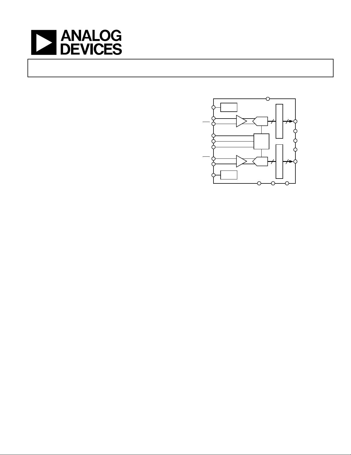
FUNCTIONAL BLOCK DIAGRAM
V
DD
T/H
T/H
AD9288
ADC
REF
ADC
D
Figure 1.
8
8
OUTPUT REGISTER
8
OUTPUT REGISTER
GNDV
8
V
DD
D7A–D0
A
SELECT 1
SELECT 2
DATA FORMAT
SELECT
–D0
D7
B
B
00585-001
ENC
AINA
AINA
REFINA
REF
OUT
REFINB
AINB
AINB
ENC
TIMING
A
TIMING
B
The Encode input is TTL/CMOS-compatible, and the 8-bit
digital outputs can be operated from 3.0 V (2.5 V to 3.6 V)
supplies. User-selectable options offer a combination of standby
modes, digital data formats, and digital data timing schemes. In
standby mode, the digital outputs are driven to a high
impedance state.
Fabricated on an advanced CMOS process, the AD9288 is
available in a 48-lead surface-mount plastic package (7 mm ×
7 mm, 1.4 mm LQFP) specified over the industrial temperature
range (–40°C to +85°C). The AD9288 is pin-compatible with
the 10-bit AD9218, facilitating future system migrations.
Rev. C
Information furnished by Analog Devices is believed to be accurate and reliable.
However, no responsibility is assumed by Analog Devices for its use, nor for any
infringements of patents or other rights of third parties that may result from its use.
Specifications subject to change without notice. No license is granted by implication
or otherwise under any patent or patent rights of Analog Devices. Trademarks and
registered trademarks are the property of their respective owners.
One Technology Way, P.O. Box 9106, Norwood, MA 02062-9106, U.S.A.
Tel: 781.329.4700
Fax: 781.326.8703 © 2004 Analog Devices, Inc. All rights reserved.
www.analog.com

AD9288
TABLE OF CONTENTS
Specifications..................................................................................... 3
Explanation of Test Levels ........................................................... 4
Timing Diagrams.......................................................................... 5
Absolute Maximum Ratings............................................................ 7
ESD Caution.................................................................................. 7
Pin Configuration and Function Descriptions............................. 8
Typical Performance Characteristics............................................. 9
Test C ir c uit s ..................................................................................... 12
Te r mi n ol o g y .................................................................................... 13
Theory of Operation ...................................................................... 14
Using the AD9288...................................................................... 14
Encode Input............................................................................... 14
Digital Outputs ........................................................................... 14
Analog Input ............................................................................... 14
Volt a ge R e fere n ce ....................................................................... 14
Timing ......................................................................................... 14
User-Selectable Options ............................................................ 14
AD9218/AD9288 Customer PCB BOM...................................... 15
Evaluation Board ............................................................................ 16
Power Connector ........................................................................ 16
Analog Inputs ............................................................................. 16
Volt a ge R e fere n ce ....................................................................... 16
Clocking....................................................................................... 16
Data Outputs............................................................................... 16
Data Format/Gain ...................................................................... 16
Timing ......................................................................................... 16
Troubleshooting.......................................................................... 20
Outline Dimensions ....................................................................... 21
Ordering Guide .......................................................................... 21
REVISION HISTORY
12/04—Rev. B to Rev. C
Change to Absolute Maximum Ratings......................................... 7
Replaced Evaluation Board Section ............................................. 16
Updated Outline Dimensions....................................................... 21
Changes to Ordering Guide.......................................................... 21
2/02—Rev. A to Rev. B
Edits to ABSOLUTE MAXIMUM RATINGS .............................. 3
1/01—Rev. 0 to Rev. A
2/99—Revision 0: Initial Version
Rev. C | Page 2 of 24

AD9288
SPECIFICATIONS
V
= 3.0 V; VD = 3.0 V, differential input; external reference, unless otherwise noted.
DD
Table 1.
Test AD9288BST-100 AD9288BST-80 AD9288BST-40
Parameter Temp Level Min Typ Max Min Typ Max Min Typ Max Unit
RESOLUTION 8 8 8 Bits
DC ACCURACY
Differential Nonlinearity 25°C I ± 0.5 +1.25 ± 0.5 +1.25 ± 0.5 +1.25 LSB
Full VI 1.50 1.50 1.50 LSB
Integral Nonlinearity 25°C I ± 0.50 +1.25 ± 0.50 +1.25 ± 0.50 +1.25 LSB
Full VI 1.50 1.50 1.50 LSB
No Missing Codes Full VI Guaranteed Guaranteed Guaranteed
Gain Error
Full VI –8 +8 –8 +8 –8 +8 % FS
Gain Tempco1 Full VI 80 80 80 ppm/°C
Gain Matching 25°C V ±1.5 ±1.5 ±1.5 % FS
Voltage Matching 25°C V ±15 ±15 ±15 mV
ANALOG INPUT
Input Voltage Range (with
Common-Mode Voltage Full V
–0.2 +0.2 –0.2 +0.2 –0.2 +0.2
Input Offset Voltage 25°C I –35 ±10 +35 –35 ± 10 +35 –35 ± 10 +35 mV
Full VI –40 +40 –40 +40 –40 +40 mV
Reference Voltage Full VI 1.2 1.25 1.3 1.2 1.25 1.3 1.2 1.25 1.3 V
Reference Tempco Full VI ± 130 ± 130 ± 130 ppm/°C
Input Resistance 25°C I 7 10 13 7 10 13 7 10 13 kΩ
Full VI 5 16 5 16 5 16
Input Capacitance 25°C V 2 2 2 pF
Analog Bandwidth, Full
SWITCHING PERFORMANCE
Maximum Conversion Rate Full VI 100 80 40 MSPS
Minimum Conversion Rate 25°C IV 1 1 1 MSPS
Encode Pulse Width High (tEH) 25°C IV 4.3 1000 5.0 1000 8.0 1000 ns
Encode Pulse Width Low (tEL) 25°C IV 4.3 1000 5.0 1000 8.0 1000 ns
Aperture Delay (tA) 25°C V 300 300 300 ps
Aperture Uncertainty (Jitter) 25°C V 5 5 5 ps rms
Output Valid Time (tV)
Output Propagation Delay
(t
DIGITAL INPUTS
Logic 1 Voltage Full VI 2.0 2.0 2.0 V
Logic 0 Voltage Full VI 0.8 0.8 0.8 V
Logic 1 Current Full VI ± 1 ± 1 ± 1 µA
Logic 0 Current Full VI ± 1 ± 1 ± 1 µA
Input Capacitance 25°C V 2.0 2.0 2.0 pF
DIGITAL OUTPUTS3
Logic 1 Voltage Full VI 2.45 2.45 2.45 V
Logic 0 Voltage Full VI 0.05 0.05 0.05 V
POWER SUPPLY
Power Dissipation4 Full VI 180 218 171 207 156 189 mW
Standby Dissipation
Power Supply Rejection
Respect to
Power
2
)
PD
Ratio (PSRR)
1
A
IN
)
2
4, 5
Full VI 6 11 6 11 6 11 mW
25°C I –6 ± 2.5 +6 –6 ± 2.5 +6 –6 ± 2.5 +6 % FS
Full V ±512 ±512 ±512 mV p-p
0.3 × VD
0.3 ×
VD
25°C V 475 475 475 MHz
Full VI 2 3.0 2 3.0 2 3.0 ns
Full VI 4.5 6.0 4.5 6.0 4.5 6.0 ns
25°C I 8 20 8 20 8 20 mV/V
0.3 ×
VD
0.3 ×
VD
0.3 × VD
0.3 ×
VD
0.3 ×
VD
0.3 × VD
0.3 ×
VD
V
Rev. C | Page 3 of 24

AD9288
Test AD9288BST-100 AD9288BST-80 AD9288BST-40
Parameter Temp Level Min Typ Max Min Typ Max Min Typ Max Unit
DYNAMIC PERFORMANCE6
Transient Response 25°C V 2 2 2 ns
Overvoltage Recovery Time 25°C V 2 2 2 ns
Signal-to-Noise Ratio (SNR)
(without Harmonics)
fIN = 10.3 MHz 25°C I 47.5 47.5 44 47.5 dB
fIN = 26 MHz 25°C I 47.5 44 47 dB
fIN = 41 MHz 25°C I 44 47.0 dB
Signal-to-Noise Ratio
(SINAD) (with Harmonics)
fIN = 10.3 MHz 25°C I 47 47 44 47 dB
fIN = 26 MHz 25°C I 47 44 47 dB
fIN = 41 MHz 25°C I 44 47 47 dB
Effective Number of Bits
fIN = 10.3 MHz 25°C I 7.5 7.5 7.0 7.5 Bits
fIN = 26 MHz 25°C I 7.5 7.0 7.5 Bits
fIN = 41 MHz 25°C I 7.0 7.5 7.5 Bits
Second Harmonic Distortion
fIN = 10.3 MHz 25°C I 70 70 55 70 dBc
fIN = 26 MHz 25°C I 70 55 70 dBc
fIN = 41 MHz 25°C I 55 70 70 dBc
Third Harmonic Distortion
fIN = 10.3 MHz 25°C I 60 60 55 60 dBc
fIN = 26 MHz 25°C I 60 55 60 dBc
fIN = 41 MHz 25°C I 52 60 60 dBc
Two-Tone Intermod
Distortion (IMD)
fIN = 10.3 MHz 25°C V 60 60 60 dBc
1
Gain error and gain temperature coefficient are based on the ADC only (with a fixed 1.25 V external reference).
2
tV and tPD are measured from the 1.5 V level of the Encode input to the 10%/90% levels of the digital outputs swing. The digital output load during test is not to exceed
an ac load of 10 pF or a dc current of ±40 µA.
3
Digital supply current based on VDD = 3.0 V output drive with < 10 pF loading under dynamic test conditions.
4
Power dissipation measured under the following conditions: f
5
Standby dissipation calculated with Encode clock in operation.
6
SNR/harmonics based on an analog input voltage of –0.7 dBFS referenced to a 1.024 V full-scale input range.
= 100 MSPS, analog input is –0.7 dBFS, both channels in operation.
S
EXPLANATION OF TEST LEVELS
Level Description
I 100% production tested.
II
III Sample tested only.
IV Parameter is guaranteed by design and characterization testing.
V Parameter is a typical value only.
VI
100% production tested at 25
100% production tested at 25
°C and sample tested at specified temperatures.
°C; guaranteed by design and characterization testing for industrial temperature range;
100% production tested at temperature extremes for military devices.
Rev. C | Page 4 of 24
AD9288
TIMING DIAGRAMS
A, AINB
A
IN
ENCODE A, B
D7
–D0
A
D7B–D0
A, AINB
A
IN
SAMPLE N SAMPLE N + 1
t
A
t
EH
A
B
DATA N – 4
DATA N – 4
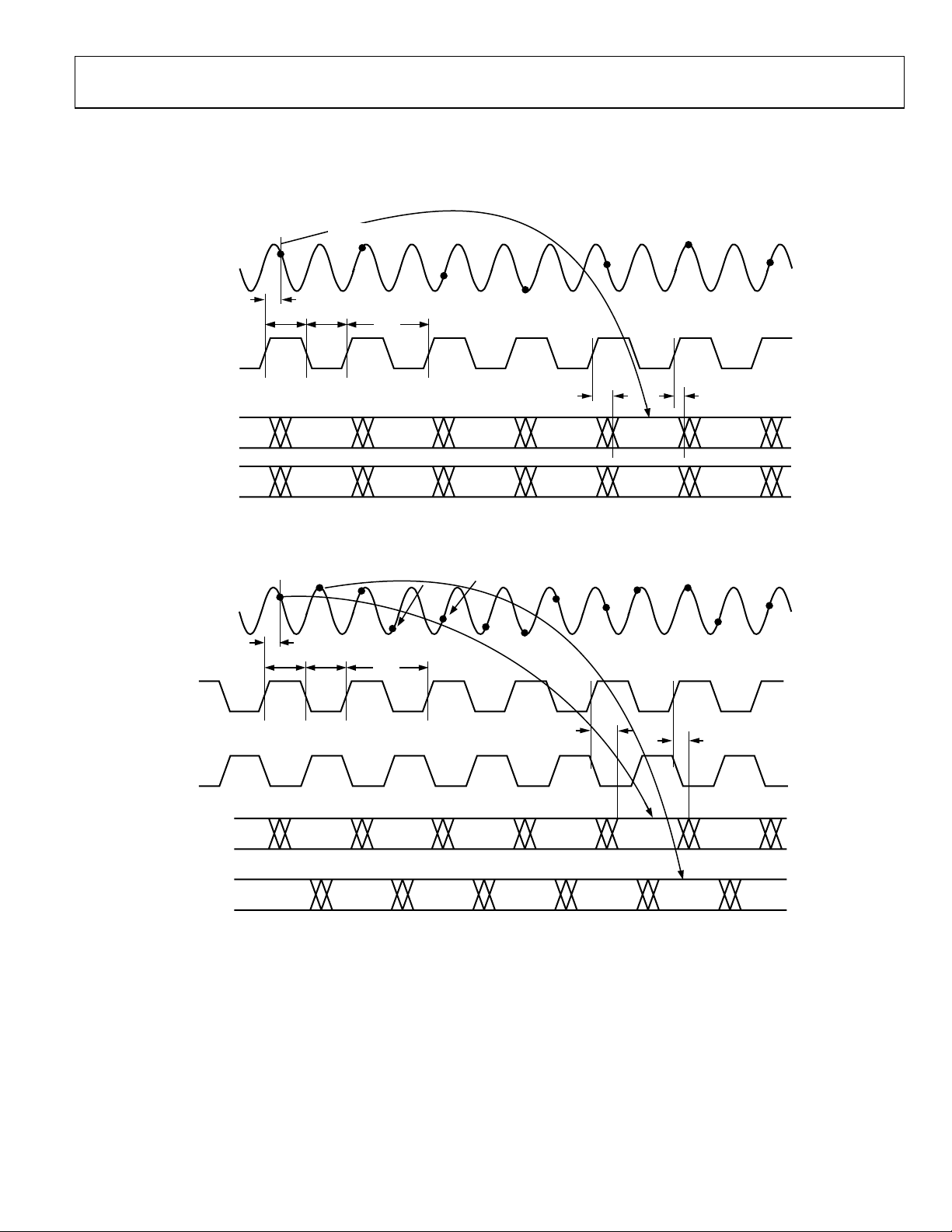
Figure 2. Normal Operation, Same Clock (S1 = 1, S2 = 0) Channel Timing
SAMPLENSAMPLE
t
A
N + 1
t
EH
SAMPLE N + 5
t
EL
SAMPLE N + 2 SAMPLE N + 3 SAMPLE N + 4
1/f
s
t
PD
DATA N – 3 DATA N – 2 DATA N – 1 DATA N DATA N + 1
DATA N – 3 DATA N – 2 DATA N – 1 DATA N DATA N + 1
t
V
00585-003
SAMPLE
N + 2
t
EL
1/f
s
SAMPLE
N + 3
SAMPLE
N + 4
ENCODE A
ENCODE B
–D0
D7
A
D7B–D0
t
PD
A
B
DATA N – 8 DATA N – 6 DATA N – 4 DATA N – 2 DATA N DATA N + 2
DATA N – 7 DATA N – 5 DATA N – 3 DATA N – 1 DATA N + 1 DATA N + 3
t
V
00585-004
Figure 3. Normal Operation with Two Clock Sources (S1 = 1, S2 = 0) Channel Timing
Rev. C | Page 5 of 24
AD9288
A
A, AINB
A
IN
ENCODE
ENCODE B
–D0
D7
A
D7B–D0
t
A
B
SAMPLENSAMPLE
A
t
EH
DATA N – 8 DATA N – 6 DATA N – 4 DATA N – 2 DATA N DATA N + 2
DATA N – 9 DATA N – 7 DATA N – 5 DATA N – 3 DATA N – 1 DATA N + 1
N + 1
t
EL
SAMPLE
N + 2
1/f
s
SAMPLE
N + 3
SAMPLE
N + 4
t
PD
t
V
00585-005
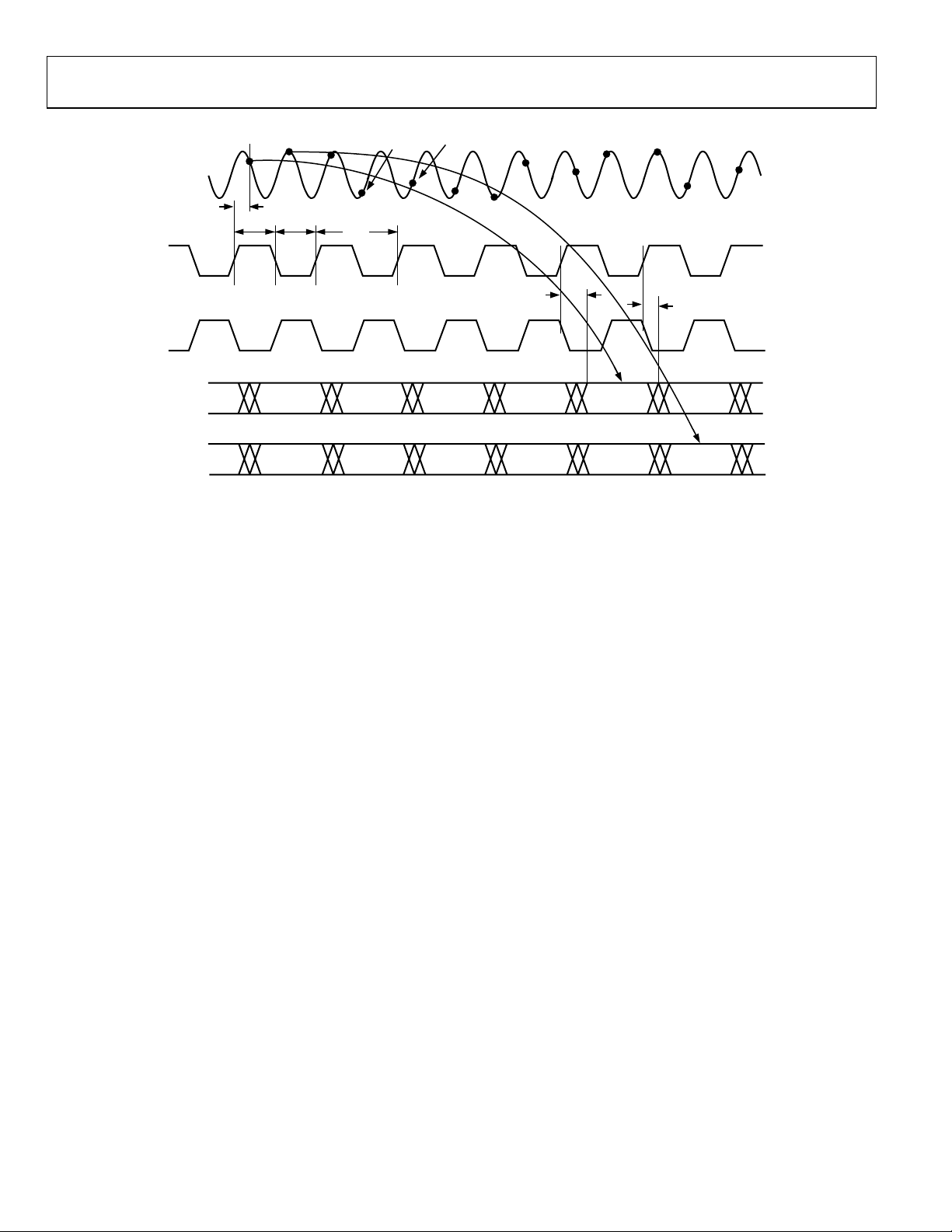
Figure 4. Data Align with Two Clock Sources (S1 = 1, S2 = 1) Channel Timing
Rev. C | Page 6 of 24
AD9288
ABSOLUTE MAXIMUM RATINGS
Table 2.
Parameter Rating
VD, V
4 V
DD
Analog Inputs –0.5 V to V
Digital Inputs –0.5 V to V
VREF IN –0.5 V to V
+ 0.5 V
D
+ 0.5 V
DD
+ 0.5 V
D
Digital Output Current 20 mA
Operating Temperature –55°C to +125°C
Storage Temperature –65°C to +150°C
Maximum Junction Temperature 150°C
Maximum Case Temperature 150°C
Thermal Impedance θ
ja
57°C/W
ESD CAUTION
ESD (electrostatic discharge) sensitive device. Electrostatic charges as high as 4000 V readily accumulate on
the human body and test equipment and can discharge without detection. Although this product features
proprietary ESD protection circuitry, permanent damage may occur on devices subjected to high energy
electrostatic discharges. Therefore, proper ESD precautions are recommended to avoid performance
degradation or loss of functionality.
Stresses above those listed under Absolute Maximum Ratings
may cause permanent damage to the device. This is a stress
rating only; functional operation of the device at these or any
other conditions outside of those indicated in the operation
sections of this specification is not implied. Exposure to
absolute maximum ratings for extended periods may affect
device reliability.
Rev. C | Page 7 of 24
AD9288
PIN CONFIGURATION AND FUNCTION DESCRIPTIONS
(MSB)
A
AD5AD4AD3AD2AD1AD0A
VDENCAVDDGND
48 47 46 45 44 39 38 3743 42 41 40
GND
1
A
IN
AINA
DFS
REF
IN
REF
OUT
REFINB
S1
S2
A
IN
A
IN
GND
NC = NO CONNECT
PIN 1
A
2
IDENTIFIER
3
4
5
A
6
7
8
9
10
B
11
B
12
13 14 15 16 17 18 19 20 21 22 23 24
D
B
V
ENC
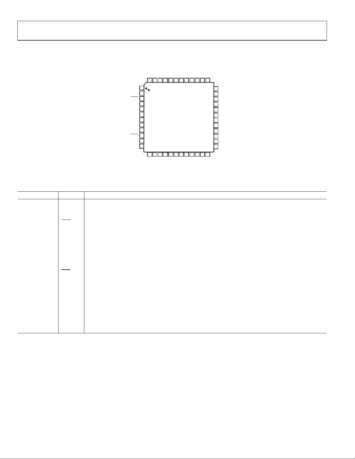
Figure 5. Pin Configuration
Table 3.
Pin No. Name Description
1, 12, 16, 27, 29,
GND Ground
32, 34, 45
2 AINA Analog Input for Channel A.
3
AINA
Analog Input for Channel A (Complementary).
4 DFS Data Format Select. Offset binary output available if set low. Twos complement output available if set high.
5 REFINA Reference Voltage Input for Channel A.
6 REF
Internal Reference Voltage.
OUT
7 REFINB Reference Voltage Input for Channel B.
8 S1 User Select 1. Refer to Table 4. Tied with respect to VD.
9 S2 User Select 2. Refer to Table 4. Tied with respect to VD.
10
AINB
Analog Input for Channel B (Complementary).
11 AINB Analog Input for Channel B.
13, 30, 31, 48 VD Analog Supply (3 V).
14 ENCB Clock Input for Channel B.
15, 28, 33, 46 VDD Digital Supply (3 V).
17–24 D7B–D0 B Digital Output for Channel B.
25, 26, 35, 36 NC Do Not Connect.
37–44 D0A–D7 A Digital Output for Channel A.
47 ENC A Clock Input for Channel A.
D6
D7
AD9288
TOP VIEW
(Not to Scale)
BD6BD5BD4BD3BD2BD1BD0B
DD
V
GND
(MSB) D7
36
NC
35
NC
34
GND
33
V
DD
32
GND
V
31
D
V
30
D
29
GND
V
28
DD
27
GND
26
NC
25
NC
00585-002
Rev. C | Page 8 of 24
 Loading...