

Page 1
8-Bit, 40/80/100 MSPS
FEATURES
Dual 8-bit, 40 MSPS, 80 MSPS, and 100 MSPS ADC
Low power: 90 mW at 100 MSPS per channel
On-chip reference and track-and-hold
475 MHz analog bandwidth each channel
SNR = 47 dB @ 41 MHz
1 V p-p analog input range each channel
Single 3.0 V supply operation (2.7 V to 3.6 V)
Standby mode for single-channel operation
Twos complement or offset binary output mode
Output data alignment mode
Pin-compatible 10-bit upgrade available
APPLICATIONS
Battery-powered instruments
Hand-held scopemeters
Low cost digital oscilloscopes
I and Q communications
GENERAL DESCRIPTION
The AD9288 is a dual 8-bit monolithic sampling analog-todigital converter with on-chip track-and-hold circuits. It is
optimized for low cost, low power, small size, and ease of use.
The product operates at a 100 MSPS conversion rate with
outstanding dynamic performance over its full operating range.
Each channel can be operated independently.
The ADC requires only a single 3.0 V (2.7 V to 3.6 V) power
supply and an Encode clock for full-performance operation. No
external reference or driver components are required for many
applications. The digital outputs are TTL/CMOS-compatible,
and a separate output power supply pin supports interfacing
with 3.3 V or 2.5 V logic.
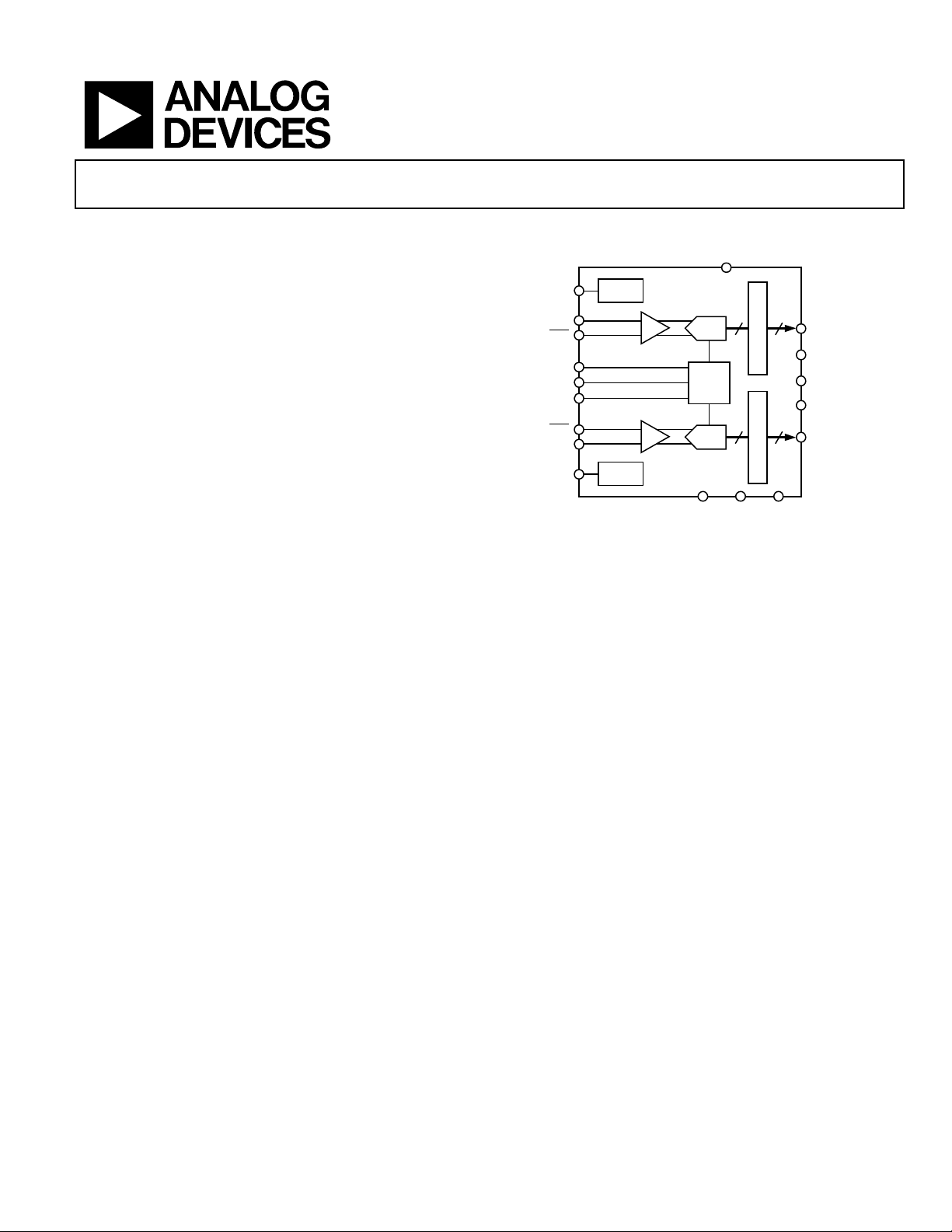
Dual A/D Converter
AD9288
FUNCTIONAL BLOCK DIAGRAM
V
DD
T/H
T/H
AD9288
ADC
REF
ADC
D
Figure 1.
8
8
OUTPUT REGISTER
8
OUTPUT REGISTER
GNDV
8
V
DD
D7A–D0
A
SELECT 1
SELECT 2
DATA FORMAT
SELECT
–D0
D7
B
B
00585-001
ENC
AINA
AINA
REFINA
REF
OUT
REFINB
AINB
AINB
ENC
TIMING
A
TIMING
B
The Encode input is TTL/CMOS-compatible, and the 8-bit
digital outputs can be operated from 3.0 V (2.5 V to 3.6 V)
supplies. User-selectable options offer a combination of standby
modes, digital data formats, and digital data timing schemes. In
standby mode, the digital outputs are driven to a high
impedance state.
Fabricated on an advanced CMOS process, the AD9288 is
available in a 48-lead surface-mount plastic package (7 mm ×
7 mm, 1.4 mm LQFP) specified over the industrial temperature
range (–40°C to +85°C). The AD9288 is pin-compatible with
the 10-bit AD9218, facilitating future system migrations.
Rev. C
Information furnished by Analog Devices is believed to be accurate and reliable.
However, no responsibility is assumed by Analog Devices for its use, nor for any
infringements of patents or other rights of third parties that may result from its use.
Specifications subject to change without notice. No license is granted by implication
or otherwise under any patent or patent rights of Analog Devices. Trademarks and
registered trademarks are the property of their respective owners.
One Technology Way, P.O. Box 9106, Norwood, MA 02062-9106, U.S.A.
Tel: 781.329.4700
Fax: 781.326.8703 © 2004 Analog Devices, Inc. All rights reserved.
www.analog.com
Page 2

AD9288
TABLE OF CONTENTS
Specifications..................................................................................... 3
Explanation of Test Levels ........................................................... 4
Timing Diagrams.......................................................................... 5
Absolute Maximum Ratings............................................................ 7
ESD Caution.................................................................................. 7
Pin Configuration and Function Descriptions............................. 8
Typical Performance Characteristics............................................. 9
Test C ir c uit s ..................................................................................... 12
Te r mi n ol o g y .................................................................................... 13
Theory of Operation ...................................................................... 14
Using the AD9288...................................................................... 14
Encode Input............................................................................... 14
Digital Outputs ........................................................................... 14
Analog Input ............................................................................... 14
Volt a ge R e fere n ce ....................................................................... 14
Timing ......................................................................................... 14
User-Selectable Options ............................................................ 14
AD9218/AD9288 Customer PCB BOM...................................... 15
Evaluation Board ............................................................................ 16
Power Connector ........................................................................ 16
Analog Inputs ............................................................................. 16
Volt a ge R e fere n ce ....................................................................... 16
Clocking....................................................................................... 16
Data Outputs............................................................................... 16
Data Format/Gain ...................................................................... 16
Timing ......................................................................................... 16
Troubleshooting.......................................................................... 20
Outline Dimensions ....................................................................... 21
Ordering Guide .......................................................................... 21
REVISION HISTORY
12/04—Rev. B to Rev. C
Change to Absolute Maximum Ratings......................................... 7
Replaced Evaluation Board Section ............................................. 16
Updated Outline Dimensions....................................................... 21
Changes to Ordering Guide.......................................................... 21
2/02—Rev. A to Rev. B
Edits to ABSOLUTE MAXIMUM RATINGS .............................. 3
1/01—Rev. 0 to Rev. A
2/99—Revision 0: Initial Version
Rev. C | Page 2 of 24
Page 3

AD9288
SPECIFICATIONS
V
= 3.0 V; VD = 3.0 V, differential input; external reference, unless otherwise noted.
DD
Table 1.
Test AD9288BST-100 AD9288BST-80 AD9288BST-40
Parameter Temp Level Min Typ Max Min Typ Max Min Typ Max Unit
RESOLUTION 8 8 8 Bits
DC ACCURACY
Differential Nonlinearity 25°C I ± 0.5 +1.25 ± 0.5 +1.25 ± 0.5 +1.25 LSB
Full VI 1.50 1.50 1.50 LSB
Integral Nonlinearity 25°C I ± 0.50 +1.25 ± 0.50 +1.25 ± 0.50 +1.25 LSB
Full VI 1.50 1.50 1.50 LSB
No Missing Codes Full VI Guaranteed Guaranteed Guaranteed
Gain Error
Full VI –8 +8 –8 +8 –8 +8 % FS
Gain Tempco1 Full VI 80 80 80 ppm/°C
Gain Matching 25°C V ±1.5 ±1.5 ±1.5 % FS
Voltage Matching 25°C V ±15 ±15 ±15 mV
ANALOG INPUT
Input Voltage Range (with
Common-Mode Voltage Full V
–0.2 +0.2 –0.2 +0.2 –0.2 +0.2
Input Offset Voltage 25°C I –35 ±10 +35 –35 ± 10 +35 –35 ± 10 +35 mV
Full VI –40 +40 –40 +40 –40 +40 mV
Reference Voltage Full VI 1.2 1.25 1.3 1.2 1.25 1.3 1.2 1.25 1.3 V
Reference Tempco Full VI ± 130 ± 130 ± 130 ppm/°C
Input Resistance 25°C I 7 10 13 7 10 13 7 10 13 kΩ
Full VI 5 16 5 16 5 16
Input Capacitance 25°C V 2 2 2 pF
Analog Bandwidth, Full
SWITCHING PERFORMANCE
Maximum Conversion Rate Full VI 100 80 40 MSPS
Minimum Conversion Rate 25°C IV 1 1 1 MSPS
Encode Pulse Width High (tEH) 25°C IV 4.3 1000 5.0 1000 8.0 1000 ns
Encode Pulse Width Low (tEL) 25°C IV 4.3 1000 5.0 1000 8.0 1000 ns
Aperture Delay (tA) 25°C V 300 300 300 ps
Aperture Uncertainty (Jitter) 25°C V 5 5 5 ps rms
Output Valid Time (tV)
Output Propagation Delay
(t
DIGITAL INPUTS
Logic 1 Voltage Full VI 2.0 2.0 2.0 V
Logic 0 Voltage Full VI 0.8 0.8 0.8 V
Logic 1 Current Full VI ± 1 ± 1 ± 1 µA
Logic 0 Current Full VI ± 1 ± 1 ± 1 µA
Input Capacitance 25°C V 2.0 2.0 2.0 pF
DIGITAL OUTPUTS3
Logic 1 Voltage Full VI 2.45 2.45 2.45 V
Logic 0 Voltage Full VI 0.05 0.05 0.05 V
POWER SUPPLY
Power Dissipation4 Full VI 180 218 171 207 156 189 mW
Standby Dissipation
Power Supply Rejection
Respect to
Power
2
)
PD
Ratio (PSRR)
1
A
IN
)
2
4, 5
Full VI 6 11 6 11 6 11 mW
25°C I –6 ± 2.5 +6 –6 ± 2.5 +6 –6 ± 2.5 +6 % FS
Full V ±512 ±512 ±512 mV p-p
0.3 × VD
0.3 ×
VD
25°C V 475 475 475 MHz
Full VI 2 3.0 2 3.0 2 3.0 ns
Full VI 4.5 6.0 4.5 6.0 4.5 6.0 ns
25°C I 8 20 8 20 8 20 mV/V
0.3 ×
VD
0.3 ×
VD
0.3 × VD
0.3 ×
VD
0.3 ×
VD
0.3 × VD
0.3 ×
VD
V
Rev. C | Page 3 of 24
Page 4
AD9288
Test AD9288BST-100 AD9288BST-80 AD9288BST-40
Parameter Temp Level Min Typ Max Min Typ Max Min Typ Max Unit
DYNAMIC PERFORMANCE6
Transient Response 25°C V 2 2 2 ns
Overvoltage Recovery Time 25°C V 2 2 2 ns
Signal-to-Noise Ratio (SNR)
(without Harmonics)
fIN = 10.3 MHz 25°C I 47.5 47.5 44 47.5 dB
fIN = 26 MHz 25°C I 47.5 44 47 dB
fIN = 41 MHz 25°C I 44 47.0 dB
Signal-to-Noise Ratio
(SINAD) (with Harmonics)
fIN = 10.3 MHz 25°C I 47 47 44 47 dB
fIN = 26 MHz 25°C I 47 44 47 dB
fIN = 41 MHz 25°C I 44 47 47 dB
Effective Number of Bits
fIN = 10.3 MHz 25°C I 7.5 7.5 7.0 7.5 Bits
fIN = 26 MHz 25°C I 7.5 7.0 7.5 Bits
fIN = 41 MHz 25°C I 7.0 7.5 7.5 Bits
Second Harmonic Distortion
fIN = 10.3 MHz 25°C I 70 70 55 70 dBc
fIN = 26 MHz 25°C I 70 55 70 dBc
fIN = 41 MHz 25°C I 55 70 70 dBc
Third Harmonic Distortion
fIN = 10.3 MHz 25°C I 60 60 55 60 dBc
fIN = 26 MHz 25°C I 60 55 60 dBc
fIN = 41 MHz 25°C I 52 60 60 dBc
Two-Tone Intermod
Distortion (IMD)
fIN = 10.3 MHz 25°C V 60 60 60 dBc
1
Gain error and gain temperature coefficient are based on the ADC only (with a fixed 1.25 V external reference).
2
tV and tPD are measured from the 1.5 V level of the Encode input to the 10%/90% levels of the digital outputs swing. The digital output load during test is not to exceed
an ac load of 10 pF or a dc current of ±40 µA.
3
Digital supply current based on VDD = 3.0 V output drive with < 10 pF loading under dynamic test conditions.
4
Power dissipation measured under the following conditions: f
5
Standby dissipation calculated with Encode clock in operation.
6
SNR/harmonics based on an analog input voltage of –0.7 dBFS referenced to a 1.024 V full-scale input range.
= 100 MSPS, analog input is –0.7 dBFS, both channels in operation.
S
EXPLANATION OF TEST LEVELS
Level Description
I 100% production tested.
II
III Sample tested only.
IV Parameter is guaranteed by design and characterization testing.
V Parameter is a typical value only.
VI
100% production tested at 25
100% production tested at 25
°C and sample tested at specified temperatures.
°C; guaranteed by design and characterization testing for industrial temperature range;
100% production tested at temperature extremes for military devices.
Rev. C | Page 4 of 24
Page 5
AD9288
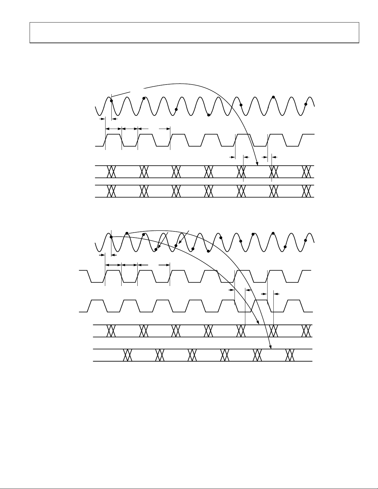
TIMING DIAGRAMS
A, AINB
A
IN
ENCODE A, B
D7
–D0
A
D7B–D0
A, AINB
A
IN
SAMPLE N SAMPLE N + 1
t
A
t
EH
A
B
DATA N – 4
DATA N – 4
Figure 2. Normal Operation, Same Clock (S1 = 1, S2 = 0) Channel Timing
SAMPLENSAMPLE
t
A
N + 1
t
EH
SAMPLE N + 5
t
EL
SAMPLE N + 2 SAMPLE N + 3 SAMPLE N + 4
1/f
s
t
PD
DATA N – 3 DATA N – 2 DATA N – 1 DATA N DATA N + 1
DATA N – 3 DATA N – 2 DATA N – 1 DATA N DATA N + 1
t
V
00585-003
SAMPLE
N + 2
t
EL
1/f
s
SAMPLE
N + 3
SAMPLE
N + 4
ENCODE A
ENCODE B
–D0
D7
A
D7B–D0
t
PD
A
B
DATA N – 8 DATA N – 6 DATA N – 4 DATA N – 2 DATA N DATA N + 2
DATA N – 7 DATA N – 5 DATA N – 3 DATA N – 1 DATA N + 1 DATA N + 3
t
V
00585-004
Figure 3. Normal Operation with Two Clock Sources (S1 = 1, S2 = 0) Channel Timing
Rev. C | Page 5 of 24
Page 6
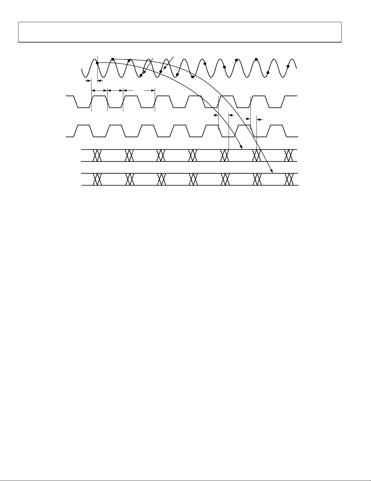
AD9288
A
A, AINB
A
IN
ENCODE
ENCODE B
–D0
D7
A
D7B–D0
t
A
B
SAMPLENSAMPLE
A
t
EH
DATA N – 8 DATA N – 6 DATA N – 4 DATA N – 2 DATA N DATA N + 2
DATA N – 9 DATA N – 7 DATA N – 5 DATA N – 3 DATA N – 1 DATA N + 1
N + 1
t
EL
SAMPLE
N + 2
1/f
s
SAMPLE
N + 3
SAMPLE
N + 4
t
PD
t
V
00585-005
Figure 4. Data Align with Two Clock Sources (S1 = 1, S2 = 1) Channel Timing
Rev. C | Page 6 of 24
Page 7
AD9288
ABSOLUTE MAXIMUM RATINGS
Table 2.
Parameter Rating
VD, V
4 V
DD
Analog Inputs –0.5 V to V
Digital Inputs –0.5 V to V
VREF IN –0.5 V to V
+ 0.5 V
D
+ 0.5 V
DD
+ 0.5 V
D
Digital Output Current 20 mA
Operating Temperature –55°C to +125°C
Storage Temperature –65°C to +150°C
Maximum Junction Temperature 150°C
Maximum Case Temperature 150°C
Thermal Impedance θ
ja
57°C/W
ESD CAUTION
ESD (electrostatic discharge) sensitive device. Electrostatic charges as high as 4000 V readily accumulate on
the human body and test equipment and can discharge without detection. Although this product features
proprietary ESD protection circuitry, permanent damage may occur on devices subjected to high energy
electrostatic discharges. Therefore, proper ESD precautions are recommended to avoid performance
degradation or loss of functionality.
Stresses above those listed under Absolute Maximum Ratings
may cause permanent damage to the device. This is a stress
rating only; functional operation of the device at these or any
other conditions outside of those indicated in the operation
sections of this specification is not implied. Exposure to
absolute maximum ratings for extended periods may affect
device reliability.
Rev. C | Page 7 of 24
Page 8
AD9288
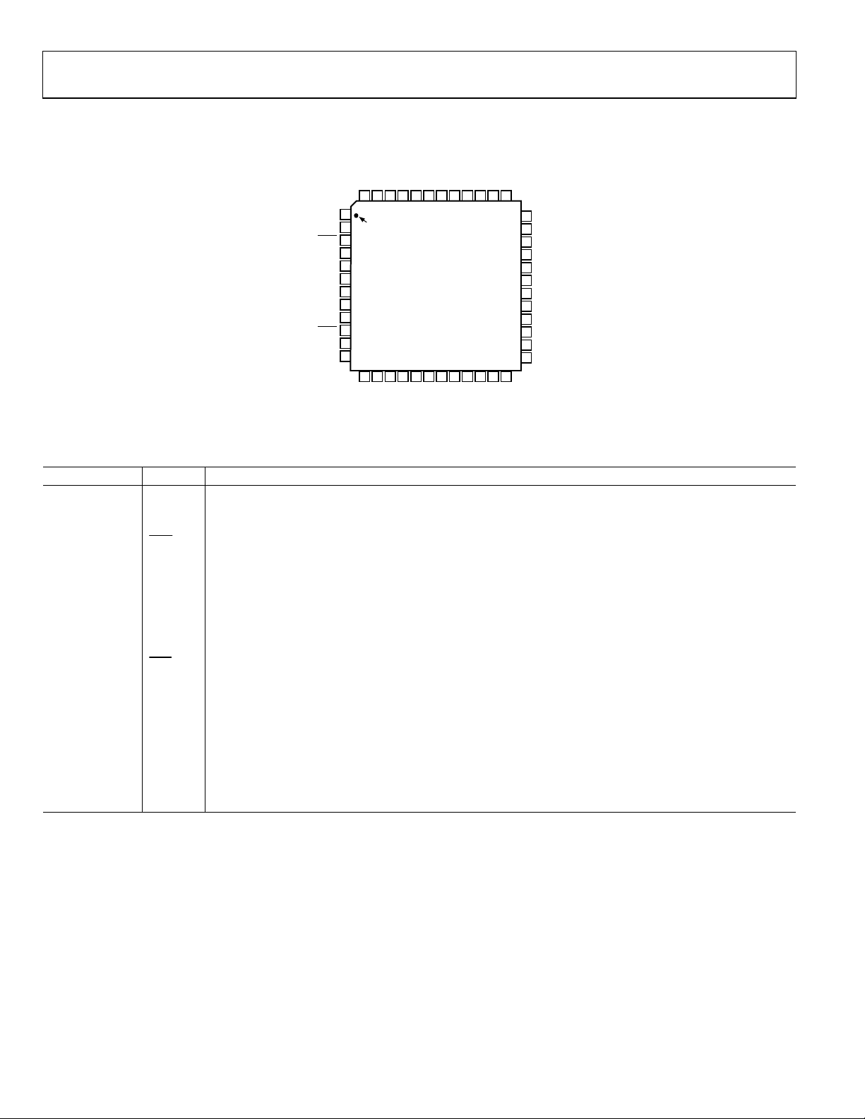
PIN CONFIGURATION AND FUNCTION DESCRIPTIONS
(MSB)
A
AD5AD4AD3AD2AD1AD0A
VDENCAVDDGND
48 47 46 45 44 39 38 3743 42 41 40
GND
1
A
IN
AINA
DFS
REF
IN
REF
OUT
REFINB
S1
S2
A
IN
A
IN
GND
NC = NO CONNECT
PIN 1
A
2
IDENTIFIER
3
4
5
A
6
7
8
9
10
B
11
B
12
13 14 15 16 17 18 19 20 21 22 23 24
D
B
V
ENC
Figure 5. Pin Configuration
Table 3.
Pin No. Name Description
1, 12, 16, 27, 29,
GND Ground
32, 34, 45
2 AINA Analog Input for Channel A.
3
AINA
Analog Input for Channel A (Complementary).
4 DFS Data Format Select. Offset binary output available if set low. Twos complement output available if set high.
5 REFINA Reference Voltage Input for Channel A.
6 REF
Internal Reference Voltage.
OUT
7 REFINB Reference Voltage Input for Channel B.
8 S1 User Select 1. Refer to Table 4. Tied with respect to VD.
9 S2 User Select 2. Refer to Table 4. Tied with respect to VD.
10
AINB
Analog Input for Channel B (Complementary).
11 AINB Analog Input for Channel B.
13, 30, 31, 48 VD Analog Supply (3 V).
14 ENCB Clock Input for Channel B.
15, 28, 33, 46 VDD Digital Supply (3 V).
17–24 D7B–D0 B Digital Output for Channel B.
25, 26, 35, 36 NC Do Not Connect.
37–44 D0A–D7 A Digital Output for Channel A.
47 ENC A Clock Input for Channel A.
D6
D7
AD9288
TOP VIEW
(Not to Scale)
BD6BD5BD4BD3BD2BD1BD0B
DD
V
GND
(MSB) D7
36
NC
35
NC
34
GND
33
V
DD
32
GND
V
31
D
V
30
D
29
GND
V
28
DD
27
GND
26
NC
25
NC
00585-002
Rev. C | Page 8 of 24
Page 9

AD9288
TYPICAL PERFORMANCE CHARACTERISTICS
0
–10
–20
–30
–40
dB
–50
–60
–70
–80
–90
Figure 6. Spectr um: f
0
ENCODE = 100MSPS
A
= 41MHz
IN
–10
SNR = 47.87dB
SINAD = 46.27dB
–20
SECOND HARMONIC = –54.10dBc
THIRD HARMONIC = –55.46dBc
–30
–40
dB
–50
–60
–70
–80
–90
Figure 7. Spectr um: f
0
–10
–20
–30
–40
dB
–50
–60
–70
–80
–90
Figure 8. Spectr um: f
ENCODE = 100MSPS
A
= 10.3MHz
IN
SNR = 48.52dB
SINAD = 48.08dB
SECOND HARMONIC = –62.54dBc
THIRD HARMONIC = –63.56dBc
SAMPLE
= 100 MSPS, fIN = 10 MHz, Single-Ended Input
S
SAMPLE
= 100 MSPS, fIN = 41 MHz, Single-Ended Input
S
ENCODE = 100MSPS
= 76MHz
A
IN
SNR = 47.1dB
SINAD = 43.2dB
SECOND
HARMONIC = –52.2dBc
THIRD HARMONIC = –51.5dBc
SAMPLE
= 100 MSPS, fIN = 76 MHz, Single-Ended Input
S
00585-006
00585-007
00585-008
72
68
64
60
56
dB
52
48
44
40
0 102030405060708090
2ND
3RD
Figure 9. Harmonic Distortion vs. A
ENCODE RATE = 100MSPS
MHz
Frequenc y
IN
0
–10
–20
–30
–40
dB
–50
–60
–70
–80
–90
SAMPLE
ENCODE = 100MSPS
1 = 9.3MHz
A
IN
2 = 10.3MHz
A
IN
IMD = –60.0dBc
Figure 10. Two-Tone Intermodulation Distortion
50
48
46
44
dB
42
40
38
36
0 102030405060708090
Figure 11. SINAD/SNR vs. A
ENCODE RATE = 100MSPS
SNR
SINAD
MHz
Frequency
IN
00585-009
00585-010
00585-011
Rev. C | Page 9 of 24
Page 10

AD9288
49
48
47
dB
46
45
50
46
42
dB
38
34
30
0.5
0
–0.5
–1.0
–1.5
–2.0
–2.5
dB
–3.0
–3.5
–4.0
–4.5
–5.0
–5.5
0 100 200 300 400 500 600
A
= 10.3MHz
IN
30 40 50 60 70 80 90 100 110
SNR
SINAD
MSPS
Figure 12. SINAD/SNR vs. Encode Rate
SNR
SINAD
7.0 6.5 6.0 5.5 5.0 4.5 4.0 3.5 3.0
ENCODE HIGH PULSE WIDTH (ns)
AIN = 10.3MHz
Figure 13. SINAD/SNR vs. Encode Pulse Width High
ENCODE RATE = 100MSPS
–3dB
BANDWIDTH (MHz)
Figure 14. ADC Frequency Response: f
= 100 MSPS
S
00585-012
00585-013
00585-014
190
185
180
175
170
165
160
POWER (mW)
155
150
145
140
0 100908070605040302010
MSPS
AIN = 10.3MHz
Figure 15. Analog Power Dissipation vs. Encode Rate
48.0
47.5
47.0
46.5
46.0
dB
45.5
45.0
44.5
44.0
43.5
–40 25 85
TEMPERATURE (°C)
ENCODE RATE = 100MSPS
= 10.3MHz
A
IN
SNR
SINAD
Figure 16. SINAD/SNR vs. Temperature
0.6
0.4
0.2
–0.2
% GAIN
–0.4
–0.6
–0.8
–1.0
0
–40 25 85
TEMPERATURE (°C)
ENCODE RATE = 100MSPS
= 10.3MHz
A
IN
Figure 17. ADC Gain vs. Temperature (with External 1.25 V Reference)
00585-015
00585-016
00585-017
Rev. C | Page 10 of 24
Page 11

AD9288
LSB
2.0
1.5
1.0
0.5
–0.5
–1.0
–1.5
–2.0
1.00
0.75
0.50
0.25
0
00585-018
CODE
Figure 18. Integral Nonlinearity
1.3
1.2
1.1
(V)
1.0
REFOUT
V
0.9
0.8
0.7
0 0.25 0.50 0.75 1.00 1.25 1.50 1.75
LOAD (mA)
ENCODE = 100MSPS
= 3.0V
V
D
= 25°C
T
A
Figure 20. Voltage Reference Out vs. Current Load
00585-020
LSB
–0.25
–0.50
–0.75
–1.00
0
00585-019
CODE
Figure 19. Differential Nonlinearity
Rev. C | Page 11 of 24
Page 12

AD9288
V
V
V
TEST CIRCUITS
D
28kΩ
A
IN
12kΩ
Figure 21. Equivalent Analog Input Circuit
V
BIAS
REF
IN
V
DD
28kΩ
A
12kΩ
IN
00585-021
OUT
00585-024
Figure 24. Equivalent Digital Output Circuit
D
00585-022
D
OUT
Figure 22. Equivalent Reference Input Circuit
00585-025
ENCODE
V
D
00585-023
Figure 25. Equivalent Reference Output Circuit
Figure 23. Equivalent Encode Input Circuit
Rev. C | Page 12 of 24
Page 13

AD9288
TERMINOLOGY
Analog Bandwidth (Small Signal)
The analog input frequency at which the spectral power of the
fundamental frequency (as determined by the FFT analysis) is
reduced by 3 dB.
Aperture Delay
The delay between a 50% crossing of Encode and the instant at
which the analog input is sampled.
Aperture Uncertainty (Jitter)
The sample-to-sample variation in aperture delay.
Differential Nonlinearity
The deviation of any code from an ideal 1 LSB step.
Encode Pulse Width/Duty Cycle
Pulse width high is the minimum amount of time that the
Encode pulse should be left in Logic 1 state to achieve rated
performance; pulse width low is the minimum time Encode
pulse should be left in low state. At a given clock rate, these
specs define an acceptable Encode duty cycle.
Integral Nonlinearity
The deviation of the transfer function from a reference line
measured in fractions of 1 LSB using a “best straight line”
determined by a least square curve fit.
Minimum Conversion Rate
The Encode rate at which the SNR of the lowest analog signal
frequency drops by no more than 3 dB below the guaranteed
limit.
Maximum Conversion Rate
The Encode rate at which parametric testing is performed.
Output Propagation Delay
The delay between a 50% crossing of Encode and the time
when all output data bits are within valid logic levels.
Power Supply Rejection Ratio
The ratio of a change in input offset voltage to a change in
power supply voltage.
Signal-to-Noise-and-Distortion (SINAD)
The ratio of the rms signal amplitude (set at 1 dB below full
scale) to the rms value of the sum of all other spectral components, including harmonics but excluding dc.
Signal-to-Noise Ratio (SNR)
The ratio of the rms signal amplitude (set at 1 dB below full
scale) to the rms value of the sum of all other spectral
components, excluding the first five harmonics and dc.
Spurious-Free Dynamic Range (SFDR)
The ratio of the rms signal amplitude to the rms value of the
peak spurious spectral component. The peak spurious component may or may not be a harmonic. May be reported in dBc
(i.e., degrades as signal level is lowered), or in dBFS (always
related back to converter full scale).
Two-Tone Intermodulation Distortion Rejection
Two -Tone SFDR
The ratio of the rms value of either input tone to the rms value
of the peak spurious component. The peak spurious component
may or may not be an IMD product. May be reported in dBc
(i.e., degrades as signal level is lowered), or in dBFS (always
related back to converter full scale).
Worst Harmonic
The ratio of the rms value of either input tone to the rms value
of the worst third order intermodulation product; reported in
dBc.
Rev. C | Page 13 of 24
Page 14

AD9288
THEORY OF OPERATION
The AD9288 ADC architecture is a bit-per-stage pipeline-type
converter utilizing switch capacitor techniques. These stages
determine the 5 MSBs and drive a 3-bit flash. Each stage
provides sufficient overlap and error correction, allowing
optimization of comparator accuracy. The input buffers are
differential, and both sets of inputs are internally biased. This
allows the most flexible use of ac or dc and differential or
single-ended input modes. The output staging block aligns the
data, carries out the error correction, and feeds the data to
output buffers. The set of output buffers are powered from a
separate supply, allowing adjustment of the output voltage
swing. There is no discernible difference in performance
between the two channels.
USING THE AD9288
Good high speed design practices must be followed when
using the AD9288. To obtain maximum benefit, decoupling
capacitors should be physically as close as possible to the chip,
minimizing trace and via inductance between chip pins and
capacitor (0603 surface-mount capacitors are used on the
AD9288/PCB evaluation board). It is recommended to place a
0.1 µF capacitor at each power-ground pin pair for high
frequency decoupling, and to include one 10 µF capacitor for
local low frequency decoupling. The VREF IN pin should also
be decoupled by a 0.1 µF capacitor. It is also recommended to
use a split power plane and a contiguous ground plane (see the
Evaluation Board section). Data output traces should be short
(< 1 inch), minimizing on-chip noise at switching.
ENCODE INPUT
Any high speed A/D converter is extremely sensitive to the
quality of the sampling clock provided by the user. A track-andhold circuit is essentially a mixer. Any noise, distortion, or
timing jitter on the clock is combined with the desired signal at
the A/D output. For that reason, considerable care has been
taken in the design of the Encode (Clock) input of the AD9288,
and the user is advised to give commensurate thought to the
clock source. The Encode input is fully TTL/CMOS-compatible.
DIGITAL OUTPUTS
The digital outputs are TTL/CMOS-compatible for lower power
consumption. During standby, the output buffers transition to a
high impedance state. A data format selection option supports
either twos complement (set high) or offset binary output (set
low) formats.
ANALOG INPUT
The analog input to the AD9288 is a differential buffer. For best
A
dynamic performance, impedance at A
IN
Special care was taken in the design of the analog input stage of
the AD9288 to prevent damage and corruption of data when
and
IN
should match.
the input is overdriven. The nominal input range is 1.024 V p-p
centered at V
× 0.3.
D
VOLTAGE REFERENCE
A stable and accurate 1.25 V voltage reference is built into the
AD9288 (REF
is used by strapping Pins 5 (REF
). In normal operation, the internal reference
OUT
A) and 7 (REFINB) to Pin 6
IN
(REFOUT). The input range can be adjusted by varying the
reference voltage applied to the AD9288. No appreciable
degradation in performance occurs when the reference is
adjusted ±5%. The full-scale range of the ADC tracks reference
voltage, which changes linearly.
TIMING
The AD9288 provides latched data outputs, with four pipeline
delays. Data outputs are available one propagation delay (t
)
PD
after the rising edge of the Encode command (see Figure 2,
Figure 3, and Figure 4). The length of the output data lines and
loads placed on them must be minimized to reduce transients
within the AD9288. These transients can detract from the
converter’s dynamic performance.
The minimum guaranteed conversion rate of the AD9288 is
1 MSPS. At clock rates below 1 MSPS, dynamic performance
degrades. Typical power-up recovery time after standby mode is
15 clock cycles.
USER-SELECTABLE OPTIONS
Two pins are available for a combination of operational modes.
These options allow the user to place both channels, excluding
the reference, into standby mode, or just the B channel. Both
modes place the output buffers and clock inputs into high
impedance states.
The other option allows the user to skew the B channel output
data by 1/2 of a clock cycle. In other words, if two clocks are fed
to the AD9288 and are 180° out of phase, enabling the data
align allows Channel B output data to be available at the rising
edge of Clock A. If the same Encode clock is provided to both
channels and the data align pin is enabled, then output data
from Channel B is 180° out of phase with respect to Channel A.
If the same Encode clock is provided to both channels and the
data align pin is disabled, both outputs are delivered on the
same rising edge of the clock.
Table 4. User-Selectable Options
S1 S2 Option
0 0 Standby Both Channels A and B.
0 1 Standby Channel B Only.
1 0 Normal Operation (Data Align Disabled).
1 1
Data Align Enabled (data from both channels available on rising edge of Clock A. Channel B data is
delayed a 1/2 clock cycle).
Rev. C | Page 14 of 24
Page 15

AD9288
AD9218/AD9288 CUSTOMER PCB BOM
Table 5. Bill of Materials
No. Qty. Reference Designator Device Package Value Comments
1 29 C1, C3-C15, C20, C21, C24,
C25, C27, C30–C35, C39–C42
2 2 C2, C36 Capacitor 0603 15 pF 8138 out
3 7 C16–C19, C26, C37, C38 Capacitor TAJD 10 µF
4 28 E1, E2, E3, E4, E12–E30,
E34–E38
5 4 H1, H2, H3, H4 MTHOLE MTHOLE
6 5 J1, J2, J3, J4, J5 SMA SMA J2, J3, not placed
7 3 P1, P4, P11 4-pin power connector Post Z5.531.3425.0 Wieland
8 3 P1, P4, P11 4-pin power connector Detachable
9 1 P2, P3
1
10 4 R1, R2, R32, R34 Resistor 0603 36 Ω R1, R2, R32, R34,
11 9 R3, R7, R11, R14, R22, R23,
R24, R30, R51
12 17 R4, R5, R8, R9, R10, R12, R13,
R20, R33, R35, R36, R37, R40,
R42, R43, R50, R53
13 2 R6, R38 Resistor 0603 25 Ω R6, R38
14 6 R15, R16, R18, R26, R29, R31 Resistor 0603 500 Ω R16, R29
15 2 R17, R25 Resistor 0603 525 Ω
16 2 R19, R27 Resistor 0603 4 kΩ
17 12 R21, R28, R39, R41, R44,
R46–R49, R52, R54, R55
18 2 T1, T2 Transformer ADT1-1WT Minicircuits
19 1 U1 AD9288
20 2 U2, U3 74LCX821
21 2 U5, U6 SN74VCX86
22 4 U7, U8, U9, U10 Resistor array CTS 47 Ω 768203470G
23 2 U11, U12 AD8138 op amp
1
P2, P3 are implemented as one physical 80-pin connector SAMTEC TSW-140-08-L-D-RA.
2
AD9288/PCB populated with AD9288-100.
3
To use optional amp: place R22, R23, R30, R24, R16, R29, remove R4, R36.
Capacitor 0603 0.1 µF
W-HOLE W-HOLE
25.602.5453.0 Wieland
Connector
80-pin rt. angle male TSW-140-08-
Samtec
L-D-RA
not placed
Resistor 0603 50 Ω R11, R22, R23,
R24, R30, R51
not placed
Resistor 0603 Zero Ω R43, R50
not placed
not placed
not placed
Resistor 0603 1 kΩ
2
3
LQFP48
Rev. C | Page 15 of 24
Page 16

AD9288
EVALUATION BOARD
The AD9218/AD9288 customer evaluation board offers an easy
way to test the AD9218 or the AD9288. The compatible pinout
of the two parts facilitates the use of one PCB for testing either
part. The PCB requires power supplies, a clock source, and a
filtered analog source for most ADC testing required.
POWER CONNECTOR
Power is supplied to the board via a detachable 12-lead power
strip. The minimum 3 V supplies required to run the board are
, VDL, and VDD. To allow the use of the optional amplifier
V
DD
path, ±5 V supplies are required.
ANALOG INPUTS
Each channel has an independent analog path that uses a
wideband transformer to drive the ADC differentially from a
single-ended sine source at the input SMAs. The transformer
paths can be bypassed to allow the use of a dc-coupled path by
using two AD8138 op amps with a simple board modification.
The analog input should be band-pass filtered to remove any
harmonics in the input signal and to minimize aliasing.
VOLTAGE REFERENCE
The AD9288 has an internal 1.25 V voltage reference; an
external reference for each channel can be used instead by
connecting two external voltage references at the power
connector and setting jumpers at E18 and E19. The evaluation
board is shipped configured for internal reference mode.
CLOCKING
Each channel can be clocked by a common clock input at SMA
input ENCODE A/B. The channels can also be clocked
independently by a simple board modification. The clock input
should be a low jitter sine source for maximum performance.
DATA OUTPUTS
The data outputs are latched on-board by two 10-bit latches and
drive an 8-pin connector which is compatible with the dualchannel FIFO board available from Analog Devices. This board,
together with ADC analyzer software, can greatly simplify ADC
testing.
DATA FORMAT/GAIN
The DFS/Gain pin can be biased for desired operation at the DFS
jumper located at the S1, S2 jumpers.
TIMING
Timing on each channel can be controlled if needed on the
PCB. Clock signals at the latches or the data ready signals that
go to the output 80-pin connector can be inverted if required.
Jumpers also allow for biasing of Pins S1 and S2 for powerdown and timing alignment control.
Rev. C | Page 16 of 24
Page 17

AD9288
VDL
VDL
E16
E38
TIEA
0.1µF
00Ω
36Ω
0.1µF
J1
R40
R14
50Ω
GND
(MSB) D9
D
V
R7
AIN B
00Ω
GND
AMPOUTB
50Ω
TIEB
C6
GND
0.1µF
GND
GND
GND
DD
V
R35
C15
GND
H3
MTHOLE6H1MTHOLE6H2MTHOLE6H4MTHOLE6
B
IN
REF
C24
0.1µF
A
IN
REF
C27
0.1µF
B
REF
C26
10µF
AV
REF
V
C19
10µF
DL
V
C18
10µF
DD
V
C17
10µF
D
C16
10µF
++++++
C38
10µF
–5V +5V V
C37
10µF
GND
–5V
123
B
A
REF
REF
V
V
123
00Ω
DLVDD
V
0.1µF
1
234
GND
+
+5V
GND
GND
ENCXB ENCB
R53
**DUT CLOCK SELECTABLE**
**TO BE DIRECT OR BUFFERED**
00Ω
**DUT CLOCK SELECTABLE**
**TO BE DIRECT OR BUFFERED**
U5
74LCX86
R50
VDL
TIEB
GND
C25
U6
74LCX86
00Ω
ENCODE B
ENCXA ENCA
E34
DRB
R12
00Ω
GND
76543
2Y
2B
GND
3Y83A93B104Y114A
E36E35
ENCXB
VDL
R52
1kΩ
R54
1kΩ
C42
0.1µF
R50
51Ω
J2
VDL
E12
E13
R46
1kΩ
VDL
0.1µF
R10
00Ω
1413121110
4B
4A4Y3B
VCC
1A11B21Y32A42B
R42
00Ω
R43
00Ω
R39
1kΩ
VDL
C40
0.1µF
TIEA
J3
ENCODE A
R48
R13
2A
R49
GND
GND
DRA
1kΩ
1kΩ
GND
GND
GND
00Ω
E15
E14
E4E3
R41
R11
CLKLATB
1Y
12
GND
5
VDL
1kΩ
50Ω
E37
VDL
R47
GND
R55
1kΩ
GND
2
1
1B
1A
C4
GND
D1AD0AGND
4B
VCC
13
14
GND
GND
A
D2
A
D3
A
D4
A
D5
A
D6
A
D7
A
D8
C41
0.1µF
VDL
D9A(MSB)
C8
0.1µF
DD
V
GND
A
ENC
D
V
C7
0.1µF
3635343332313029282726
A
D1AD0
A
37
D2
A
38
D3
A
D4
39
A
40
D5
A
D6
41
A
D7
42
A
D8
43
A
44
D9
GND
45
DD
46
V
A
ENC
47
D
48
V
A
IN
GND
A
123456789
0.1µF
GND
A
IN
A
C3
DD
V
DD
V
DFS/GAIN
D
V
0.1µF
GND
GND
DVD
V
GND
GND
U1
AD9218/AD9288
A
B
IN
OUT
IN
REF
REF
S1S2A
REF
DD
V
DD
V
C1
0.1µF
GND
D0BD1
BD1B
D0
GND
B
B
IN
IN
A
101112
GND
B
25
B
GND
GND
GND
GND
1kΩ
CLKLATA
R9
00Ω
9
8
3Y
3A
2Y
GND
6
7
C10
0.1µF
R4
GND
ENCXA
GND
R44
1kΩ
R33
00Ω
C11
0.1µF
GND
R1
AMPOUTA
R3
E25
C9
0.1µF
VD
00Ω
GND
GND
36Ω
C14
C31
0.1µF
50Ω
0.1µF
AMPINA
E30E2
R5
R2
6
1
00Ω
36Ω
5
2
GND
E17
E18E1E19
E20
GND
VREFA
GND
E27
REFOUT
R6
25Ω
AMPOUTAB
T2
34
GND
E24
GND
GND
E29
VD
R SINGLE-ENDED
E22
E23
VD E28
E26
GND
C30
0.1µF
R38
25Ω
AMPOUTBB
R SINGLE-ENDED
GND
C12
0.1µF
B
B
B
B
B
B
B
B
DD
D
R37
00Ω
R34
6
1
GND
TO TIE CLOCKS TOGETHER
D2
24
D3
23
D4
22
D5
21
D6
20
D7
19
D8
18
D9
17
GND
16
V
15
ENC
14
V
13
GND
36Ω
5
34
2
B
ENC
R20
00Ω
R8
00Ω
A
J5
ENC
B
D2
B
D3
B
D4
B
D5
B
D6
B
D7
B
D8
B
GND
B
ENC
C5
0.1µF
GND
C39
R36
GND
R32
T1
C13
AMPINB
GND
GND
AIN A
J4
GND
GND
GND
GND
4
GND
4
D
V
DDVDVDL
V
P6P5P7
P11
P4
P1
00585-026
Figure 26. PCB Schematic
Rev. C | Page 17 of 24
Page 18

AD9288
GND
DRA
GND
D9P
D8P
D7P
D6P
D5P
D4P
D3P
D2P
D1P
D0P
GND
GND
GND
GND
GND
GND
GND
3937353331
393735333129272523211917151311
2927252321
1917151311
P3
HEADER40
40383634323028262422201816141210864
4038363432
D9P
D8P
2019181716
201918171615141312
U9
CTS20
VALUE = 50
123456789
1
D9X
D8X2D7X3D6X4D5X
VDL
D9X
C21
0.1µF
2423222120
Y0Y1Y2Y3Y4Y5Y6Y7Y8
VCC
D7P
D8X
D6P
D7X
3028262422
D5P
D4P
D3P
D2P
1514131211
5
D4X6D3X7D2X8D1X9D0X
D6X
D5X
D4X
D3X
1918171615
D1P
D2X
D0P
11
10
10
D1X
2018161412
D0X
CLKLATA
14
13
U2
74LCX821
OEX0X1X2X3X4X5X6X7
1
5
X8
X9 Y9
GND CLK
11
10
12
97531
97531
864
10
GND
2
2
GND
GND
GND
DRB
GND
D9Q
D8Q
D7Q
D6Q
D5Q
D4Q
D3Q
D2Q
D1Q
D0Q
3937353331
393735333129272523211917151311
2927252321
1917151311
P2
HEADER40
40383634323028262422201816141210864
4038363432
D0Q
D1Q
2019181716
201918171615141312
U10
CTS20
VALUE = 50
123456789
1
D0Y
D1Y2D2Y3D3Y4D4Y
VDL
D0Y
C20
0.1µF
2423222120
Y0Y1Y2Y3Y4Y5Y6Y7Y8
VCC
D2Q
D1Y
D3Q
D2Y
3028262422
D4Q
D5Q
D6Q
D7Q
1514131211
5
D5Y6D6Y7D7Y8D8Y9D9Y
D3Y
D4Y
D5Y
D6Y
1918171615
D8Q
D7Y
D9Q
11
10
10
D8Y
2018161412
D9Y
CLKLATB
14
13
U3
74LCX821
OEX0X1X2X3X4X5X6X7
1
5
X8
X9 Y9
GND CLK
11
10
12
GND
GND
GND
GND
GND
97531
97531
864
10
GND
GND
2
2
00585-027
GND
D9M2D8M3D7M4D6M
GND
D9M
D8M
2019181716
201918171615141312
U7
CTS20
VALUE = 50
123456789
D9A1D8A2D7A3D6A4D5A
R16
D7M
525Ω
D6M
D5M6D4M7D3M8D2M9D1M
D5M
D4M
D3M
1514131211
5
D4A6D3A7D2A8D1A9D0A
R19
4kΩ
+5V
R18
D2M
500Ω
R21
+5V
D1M
1kΩ
C32
0.1µF
D0M
11
10
10
GND
D0M
AMPINA
123
4
U11
V+
–IN
+OUT
VOCM
AD8138
+IN8NC7V–6–OUT
5
OPAMP INPUT OFF PIN ONE OF TRANSFORMER
GND
R17
500Ω
C33
0.1µF
–5V
GND
GND
C2
R22
R23
50Ω
15pF
50Ω
AMPOUTAAMPOUTAB
D0N2D1N3D2N4D3N
GND
D0N
D1N
D2N
2019181716
201918171615141312
U8
CTS20
VALUE = 50
123456789
D0B1D1B2D2B3D3B4D4B
R25
525Ω
GND
AMPINB
R29
500Ω
D4N6D5N7D6N8D7N9D8N
D3N
D4N
D5N
1514131211
5
D5B6D6B7D7B8D8B9D9B
R27
+5V
123
–IN
AD8138
+IN8NC7V–6–OUT
4kΩ
D6N
R26
VOCM
D7N
500Ω
R28
+5V
V+
–5V
1kΩ
D8N
C35
C34
D9N
GND
D9N
11
10
10
GND
0.1µF
GND
R30
50Ω
4
U12
AMPOUTBBAMPOUTB
+OUT
C36
15pF
5
R24
50Ω
0.1µF
R15
500Ω
R31
500Ω
Figure 27. PCB Schematic (Continued)
Rev. C | Page 18 of 24
Page 19

AD9288
Figure 28. Top Silkscreen
Figure 29. Top Routing
00585-028
00585-029
Figure 31. Split Power Plane
Figure 32. Bottom Routing
00585-031
00585-032
00585-033
00585-030
Figure 30. Ground Plane
Figure 33. Bottom Silkscreen
Rev. C | Page 19 of 24
Page 20

AD9288
TROUBLESHOOTING
If the board does not seem to be working correctly, try the
following:
• Ve r if y pow e r at t he I C pins .
• Check that all jumpers are in the correct position for the
desired mode of operation.
• Ve r if y th a t V
• Try running Encode clock and analog inputs at low speeds
(20 MSPS/1 MHz) and monitor LCX821 outputs, DAC
outputs, and ADC outputs for toggling.
is at 1.23 V.
REF
The AD9218/AD9288 evaluation board is provided as a design
example for customers of Analog Devices, Inc. ADI makes no
warranties, express, statutory, or implied, regarding
merchantability or fitness for a particular purpose.
Rev. C | Page 20 of 24
Page 21

AD9288
OUTLINE DIMENSIONS
1.45
1.40
1.35
0.15
0.05
ROTATED 90° CCW
10°
6°
2°
SEATING
PLANE
VIEW A
0.75
0.60
0.45
SEATING
PLANE
0.20
0.09
7°
°
3.5
0°
0.08 MAX
COPLANARITY
COMPLIANT TO JEDEC STANDARDS MS-026BBC
1.60
MAX
VIEW A
Figure 34. 48-Lead Low Profile Quad Flat Package [LQFP]
(ST-48)
Dimensions shown in millimeters
ORDERING GUIDE
Model Temperature Range Package Description Package Options
48-Lead Low Profile Quad Flat Package
48-Lead Low Profile Quad Flat Package
48-Lead Low Profile Quad Flat Package
48-Lead Low Profile Quad Flat Package
48-Lead Low Profile Quad Flat Package
48-Lead Low Profile Quad Flat Package
48-Lead Low Profile Quad Flat Package
1
1
–40°C to +85°C
–40°C to +85°C
–40°C to +85°C
–40°C to +85°C
–40°C to +85°C
–40°C to +85°C
–40°C to +85°C
AD9288BST-40
AD9288BSTZ-40
1
AD9288BSTZRL-40
AD9288BST-80
AD9288BSTZ-80
1
AD9288BST-100
AD9288BSTZ-100
AD9288/PCB Evaluation Board
1
12
0.50
BSC
48
13
9.00 BSC
SQ
PIN 1
TOP VIEW
(PINS DOWN)
24
37
0.27
0.22
0.17
36
25
7.00
BSC SQ
ST-48
ST-48
ST-48
ST-48
ST-48
ST-48
ST-48
1
Z = Pb-free part.
Rev. C | Page 21 of 24
Page 22

AD9288
NOTES
Rev. C | Page 22 of 24
Page 23

AD9288
NOTES
Rev. C | Page 23 of 24
Page 24

AD9288
NOTES
© 2004 Analog Devices, Inc. All rights reserved. Trademarks and
registered trademarks are the property of their respective owners.
C00585–0–12/04(C)
Rev. C | Page 24 of 24
 Loading...