8-Bit, 40/80/100 MSPS
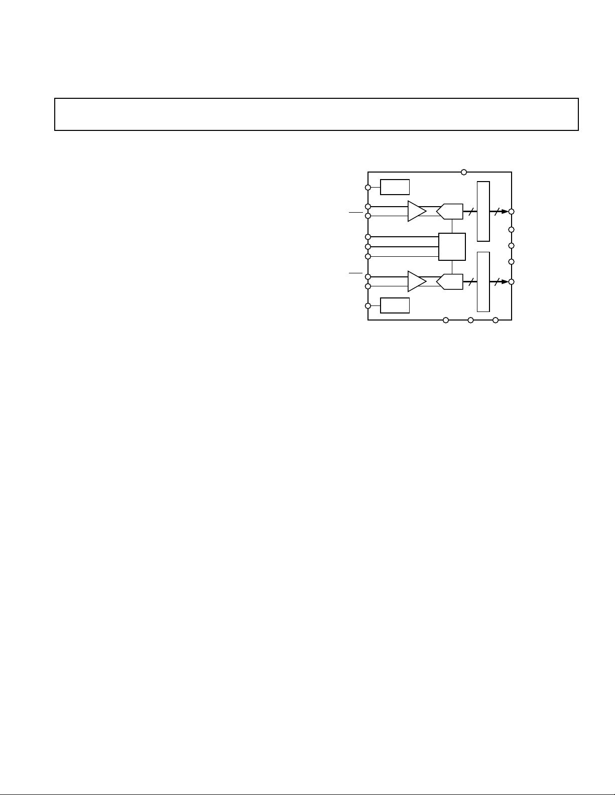
T/H
ADC
REF
T/H
ADC
OUTPUT REGISTER
8
8
8
8
OUTPUT REGISTER
TIMING
TIMING
AD9288
V
DD
D7A–D0
A
SELECT #1
SELECT #2
DATA FORMAT
SELECT
D7B–D0
B
ENC
A
AINA
A
IN
A
REFINA
REF
OUT
REFINB
A
IN
B
AINB
ENC
B
VDGND V
DD
a
FEATURES
Dual 8-Bit, 40 MSPS, 80 MSPS, and 100 MSPS ADC
Low Power: 90 mW at 100 MSPS per Channel
On-Chip Reference and Track/Holds
475 MHz Analog Bandwidth Each Channel
SNR = 47 dB @ 41 MHz
1 V p-p Analog Input Range Each Channel
Single +3.0 V Supply Operation (2.7 V–3.6 V)
Standby Mode for Single Channel Operation
Twos Complement or Offset Binary Output Mode
Output Data Alignment Mode
APPLICATIONS
Battery Powered Instruments
Hand-Held Scopemeters
Low Cost Digital Oscilloscopes
I and Q Communications
GENERAL DESCRIPTION
The AD9288 is a dual 8-bit monolithic sampling analog-todigital converter with on-chip track-and-hold circuits and is
optimized for low cost, low power, small size and ease of use.
The product operates at a 100 MSPS conversion rate with outstanding dynamic performance over its full operating range.
Each channel can be operated independently.
The ADC requires only a single 3.0 V (2.7 V to 3.6 V) power
supply and an encode clock for full-performance operation. No
external reference or driver components are required for many
applications. The digital outputs are TTL/CMOS compatible
and a separate output power supply pin supports interfacing
with 3.3 V or 2.5 V logic.
Dual A/D Converter
AD9288
FUNCTIONAL BLOCK DIAGRAM
The encode input is TTL/CMOS compatible and the 8-bit
digital outputs can be operated from +3.0 V (2.5 V to 3.6 V)
supplies. User-selectable options are available to offer a combination of standby modes, digital data formats and digital data
timing schemes. In standby mode, the digital outputs are driven
to a high impedance state.
Fabricated on an advanced CMOS process, the AD9288 is avail-
able in a 48-lead surface mount plastic package (7 × 7 mm,
1.4 mm LQFP) specified over the industrial temperature range
(–40°C to +85°C).
One Technology Way, P.O. Box 9106, Norwood, MA 02062-9106, U.S.A.
Tel: 781/329-4700 World Wide Web Site: http://www.analog.com
Fax: 781/326-8703 © Analog Devices, Inc., 1999
REV. 0
Information furnished by Analog Devices is believed to be accurate and
reliable. However, no responsibility is assumed by Analog Devices for its
use, nor for any infringements of patents or other rights of third parties
which may result from its use. No license is granted by implication or
otherwise under any patent or patent rights of Analog Devices.

AD9288–SPECIFICATIONS
(VDD = 3.0 V; VD = 3.0 V, Differential Input; External reference unless otherwise noted.)
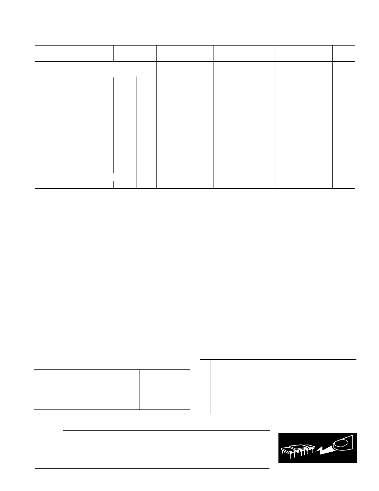
Test AD9288BST-100 AD9288BST-80 AD9288BST-40
Parameter Temp Level Min Typ Max Min Typ Max Min Typ Max Units
RESOLUTION 8 8 8 Bits
DC ACCURACY
Differential Nonlinearity +25°CI ±0.5 +1.25 ±0.5 +1.25 ±0.5 +1.25 LSB
Full VI +1.50 +1.50 +1.50 LSB
Integral Nonlinearity +25°CI ±0.50 +1.25 ±0.50 +1.25 ±0.50 +1.25 LSB
Full VI +1.50 +1.50 +1.50 LSB
No Missing Codes Full VI Guaranteed Guaranteed Guaranteed
Gain Error
Gain Tempco
1
1
+25°CI –6 ±2.5 +6 –6 ±2.5 +6 –6 ±2.5 +6 % FS
Full VI –8 +8 –8 +8 –8 +8 % FS
Full VI 80 80 80 ppm/°C
Gain Matching +25°CV ±1.5 ±1.5 ±1.5 % FS
Voltage Matching +25°CV ±15 ±15 ±15 mV
ANALOG INPUT
Input Voltage Range
(With Respect to AIN) Full V ±512 ±512 ±512 mV p-p
Common-Mode Voltage Full V ±200 ±200 ±200 mV
Input Offset Voltage +25°C I –35 ±10 +35 –35 ±10 +35 –35 ±10 +35 mV
Full VI ±40 ±40 ±40 mV
Reference Voltage Full VI 1.2 1.25 1.3 1.2 1.25 1.3 1.2 1.25 1.3 V
Reference Tempco Full VI ±130 ±130 ±130 ppm/°C
Input Resistance +25°C I 7 10 13 7 10 13 7 10 13 kΩ
Full VI 5 16 5 16 5 16 kΩ
Input Capacitance +25°CV 2 2 2 pF
Analog Bandwidth, Full Power +25°C V 475 475 475 MHz
SWITCHING PERFORMANCE
Maximum Conversion Rate Full VI 100 80 40 MSPS
Minimum Conversion Rate +25°CIV111MSPS
Encode Pulsewidth High (t
Encode Pulsewidth Low (t
Aperture Delay (t
) +25°CV 0 0 0 ns
A
Aperture Uncertainty (Jitter) +25°C V 5 5 5 ps rms
Output Valid Time (t
) +25°C IV 4.3 1000 5.0 1000 8.0 1000 ns
EH
) +25°C IV 4.3 1000 5.0 1000 8.0 1000 ns
EL
2
)
V
Full VI 3.0 3.0 3.0 ns
Output Propagation Delay (tPD)2Full VI 4.5 4.5 4.5 ns
DIGITAL INPUTS
Logic “1” Voltage Full VI 2.0 2.0 2.0 V
Logic “0” Voltage Full VI 0.8 0.8 0.8 V
Logic “1” Current Full VI ±1 ±1 ±1 µA
Logic “0” Current Full VI ±1 ±1 ±1 µA
Input Capacitance +25°C V 2.0 2.0 2.0 pF
DIGITAL OUTPUTS
3
Logic “1” Voltage Full VI 2.45 2.45 2.45 V
Logic “0” Voltage Full VI 0.05 0.05 0.05 V
POWER SUPPLY
Power Dissipation
Standby Dissipation
4
4, 5
Full VI 180 218 171 207 156 189 mW
Full VI 6 11 6 11 6 11 mW
Power Supply Rejection Ratio
(PSRR) +25°C I 8 20 8 20 8 20 mV/V
DYNAMIC PERFORMANCE
6
Transient Response +25°CV 2 2 2 ns
Overvoltage Recovery Time +25°CV 2 2 2 ns
Signal-to-Noise Ratio (SNR)
(Without Harmonics)
f
= 10.3 MHz +25°C I 47.5 47.5 44 47.5 dB
IN
= 26 MHz +25°C I 47.5 44 47 dB
f
IN
f
= 41 MHz +25°C I 44 47.0 dB
IN
–2–
REV. 0

AD9288
Test AD9288BST-100 AD9288BST-80 AD9288BST-40
Parameter Temp Level Min Typ Max Min Typ Max Min Typ Max Units
DYNAMIC PERFORMANCE
Signal-to-Noise Ratio (SINAD) (With Harmonics)
f
= 10.3 MHz +25°C I 47 47 44 47 dB
IN
f
= 26 MHz +25°C I 47 44 47 dB
IN
f
= 41 MHz +25°C I 44 47 47 dB
IN
Effective Number of Bits
f
= 10.3 MHz +25°C I 7.5 7.5 7.0 7.5 Bits
IN
f
= 26 MHz +25°C I 7.5 7.0 7.5 Bits
IN
= 41 MHz +25°C I 7.0 7.5 7.5 Bits
f
IN
2nd Harmonic Distortion
= 10.3 MHz +25°C I 70 70 55 70 dBc
f
IN
f
= 26 MHz +25°C I 70 55 70 dBc
IN
= 41 MHz +25°C I 55 70 70 dBc
f
IN
3rd Harmonic Distortion
= 10.3 MHz +25°C I 60 60 55 60 dBc
f
IN
f
= 26 MHz +25°C I 60 55 60 dBc
IN
= 41 MHz +25°C I 52 60 60 dBc
f
IN
Two-Tone Intermod Distortion (IMD)
f
= 10.3 MHz +25°C V 60 60 60 dBc
IN
NOTES
1
Gain error and gain temperature coefficient are based on the ADC only (with a fixed 1.25 V external reference).
2
tV and tPD are measured from the 1.5 V level of the ENCODE input to the 10%/90% levels of the digital outputs swing. The digital output load during test is not to
exceed an ac load of 10 pF or a dc current of ±40 µA.
3
Digital supply current based on VDD = +3.0 V output drive with <10 pF loading under dynamic test conditions.
4
Power dissipation measured under the following conditions: fS = 100 MSPS, analog input is –0.7 dBFS, both channels in operation.
5
Standby dissipation calculated with encode clock in operation.
6
SNR/harmonics based on an analog input voltage of –0.7 dBFS referenced to a 1.024 V full-scale input range.
Specifications subject to change without notice.
ABSOLUTE MAXIMUM RATINGS*
VD, VDD . . . . . . . . . . . . . . . . . . . . . . . . . . . . . . . . . . . . . . +4 V
Analog Inputs . . . . . . . . . . . . . . . . . . . . –0.5 V to V
Digital Inputs . . . . . . . . . . . . . . . . . . . –0.5 V to V
VREF IN . . . . . . . . . . . . . . . . . . . . . . . . –0.5 V to V
Digital Output Current . . . . . . . . . . . . . . . . . . . . . . . . 20 mA
Operating Temperature . . . . . . . . . . . . . . . . –55°C to +125°C
Storage Temperature . . . . . . . . . . . . . . . . . . –65°C to +150°C
Maximum Junction Temperature . . . . . . . . . . . . . . . +175°C
Maximum Case Temperature . . . . . . . . . . . . . . . . . . +150°C
*Stresses above those listed under Absolute Maximum Ratings may cause perma-
nent damage to the device. This is a stress rating only; functional operation of the
device at these or any other conditions outside of those indicated in the operation
sections of this specification is not implied. Exposure to absolute maximum
ratings for extended periods may affect device reliability.
Model Ranges Options
AD9288BST
-40, -80, -100 –40°C to +85°C ST-48*
AD9288/PCB +25°C Evaluation Board
*ST = Thin Plastic Quad Flatpack (1.4 mm thick, 7 × 7 mm: LQFP).
6
(Continued)
ORDERING GUIDE
Temperature Package
+ 0.5 V
D
+ 0.5 V
DD
+ 0.5 V
D
EXPLANATION OF TEST LEVELS
Test Level
I 100% production tested.
II 100% production tested at +25°C and sample tested at
specified temperatures.
III Sample tested only.
IV Parameter is guaranteed by design and characterization
testing.
V Parameter is a typical value only.
VI 100% production tested at +25°C; guaranteed by design
and characterization testing for industrial temperature
range; 100% production tested at temperature extremes for
military devices.
Table I. User Select Options
S1 S2 User Select Options
0 0 Standby Both Channels A and B.
0 1 Standby Channel B Only.
1 0 Normal Operation (Data Align Disabled).
1 1 Data align enabled (data from both channels avail-
able on rising edge of Clock A. Channel B data is
delayed a 1/2 clock cycle).
CAUTION
ESD (electrostatic discharge) sensitive device. Electrostatic charges as high as 4000 V readily
accumulate on the human body and test equipment and can discharge without detection.
Although the AD9288 features proprietary ESD protection circuitry, permanent damage may
occur on devices subjected to high energy electrostatic discharges. Therefore, proper ESD
precautions are recommended to avoid performance degradation or loss of functionality.
REV. 0 –3–
WARNING!
ESD SENSITIVE DEVICE

AD9288
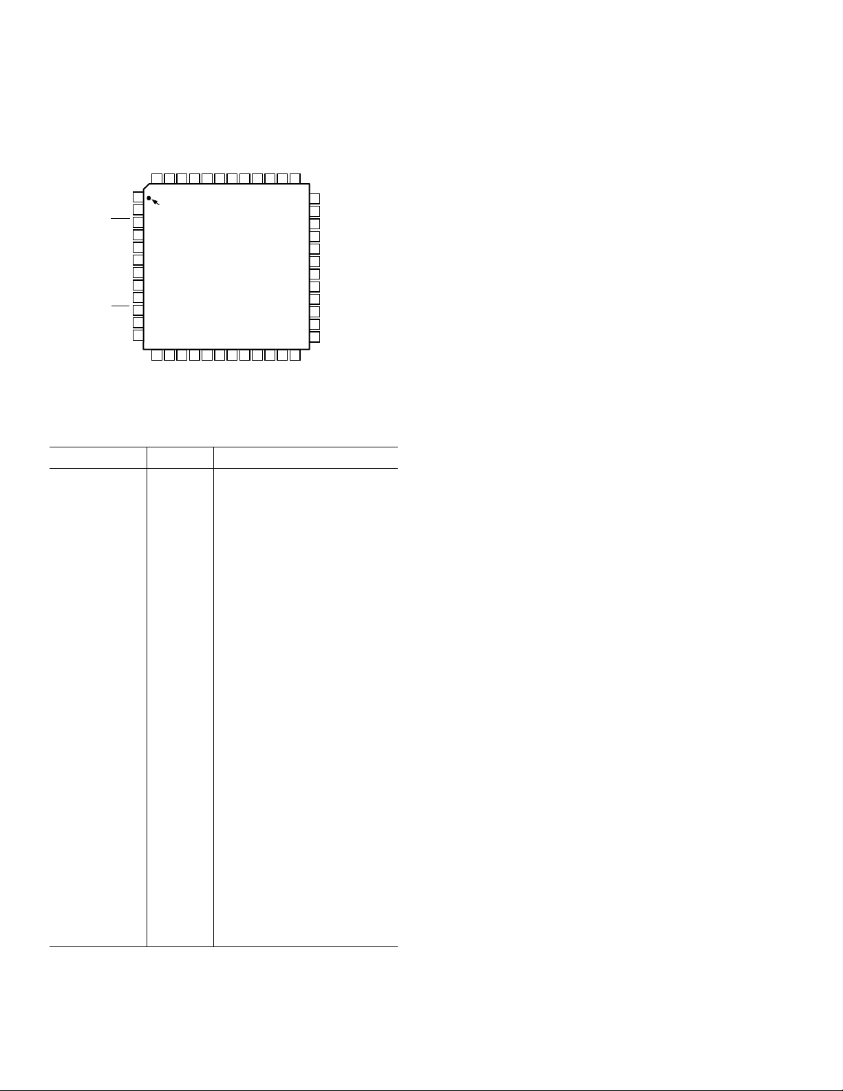
PIN CONFIGURATION
A
GND
A
A
IN
A
A
IN
DFS
REF
A
IN
REF
OUT
REFINB
S1
S2
10
A
B
IN
11
A
B
IN
GND
12
NC = NO CONNECT
(MSB)
A
ENC
B
ENC
DD
V
DD
V
A
GND
D6
D7
AD9288
TOP VIEW
(Not to Scale)
B
B
D6
GND
(MSB) D7
D
V
48 47 46 45 44 39 38 3743 42 41 40
1
PIN 1
2
IDENTIFIER
3
4
5
6
7
8
9
13 14 15 16 17 18 19 20 21 22 23 24
D
V
A
A
A
A
A
D4
D5
B
B
D4
D5
A
D2
D1
D3
D0
36
NC
35
NC
34
GND
V
33
DD
32
GND
31
V
D
30
V
D
29
GND
V
28
DD
27
GND
26
NC
25
NC
B
B
B
B
D1
D2
D0
D3
PIN FUNCTION DESCRIPTIONS
Pin No. Name Description
1, 12, 16, 27, 29,
32, 34, 45 GND Ground.
2A
A Analog Input for Channel A.
IN
3 AINA Analog Input for Channel A
(Complementary).
4 DFS Data Format Select: (Offset
binary output available if set
low. Twos complement output
available if set high).
5 REF
A Reference Voltage Input for
IN
Channel A.
6 REF
7 REF
OUT
IN
Internal Reference Voltage.
B Reference Voltage Input for
Channel B.
8 S1 User Select #1 (Refer to Table
I), Tied with Respect to V
.
D
9 S2 User Select #2 (Refer to Table
I), Tied with Respect to V
.
D
10 AINB Analog Input for Channel B
(Complementary).
11 A
13, 30, 31, 48 V
14 ENC
15, 28, 33, 46 V
17–24 D7
B Analog Input for Channel B.
IN
D
B
DD
–D0BDigital Output for Channel B.
B
Analog Supply (3 V).
Clock Input for Channel B.
Digital Supply (3 V).
25, 26, 35, 36 NC Do Not Connect.
37–44 D0
47 ENC
–D7ADigital Output for Channel A.
A
A
Clock Input for Channel A.
DEFINITION OF SPECIFICATIONS
Analog Bandwidth (Small Signal)
The analog input frequency at which the spectral power of the
fundamental frequency (as determined by the FFT analysis) is
reduced by 3 dB.
–4–
Aperture Delay
The delay between a differential crossing of ENCODE and
ENCODE and the instant at which the analog input is sampled.
Aperture Uncertainty (Jitter)
The sample-to-sample variation in aperture delay.
Differential Nonlinearity
The deviation of any code from an ideal 1 LSB step.
Encode Pulsewidth/Duty Cycle
Pulsewidth high is the minimum amount of time that the ENCODE pulse should be left in Logic “1” state to achieve rated
performance; pulsewidth low is the minimum time ENCODE
pulse should be left in low state. At a given clock rate, these
specs define an acceptable Encode duty cycle.
Integral Nonlinearity
The deviation of the transfer function from a reference line
measured in fractions of 1 LSB using a “best straight line” determined by a least square curve fit.
Minimum Conversion Rate
The encode rate at which the SNR of the lowest analog signal
frequency drops by no more than 3 dB below the guaranteed
limit.
Maximum Conversion Rate
The encode rate at which parametric testing is performed.
Output Propagation Delay
The delay between a differential crossing of ENCODE and
ENCODE and the time when all output data bits are within
valid logic levels.
Power Supply Rejection Ratio
The ratio of a change in input offset voltage to a change in
power supply voltage.
Signal-to-Noise-and-Distortion (SINAD)
The ratio of the rms signal amplitude (set at 1 dB below full
scale) to the rms value of the sum of all other spectral components, including harmonics but excluding dc.
Signal-to-Noise Ratio (SNR)
The ratio of the rms signal amplitude (set at 1 dB below full
scale) to the rms value of the sum of all other spectral components, excluding the first five harmonics and dc.
Spurious-Free Dynamic Range (SFDR)
The ratio of the rms signal amplitude to the rms value of the
peak spurious spectral component. The peak spurious component may or may not be a harmonic. May be reported in dBc
(i.e., degrades as signal levels is lowered), or in dBFS (always
related back to converter full scale).
Two-Tone Intermodulation Distortion Rejection
The ratio of the rms value of either input tone to the rms
value of the worst third order intermodulation product; reported in dBc.
Two-Tone SFDR
The ratio of the rms value of either input tone to the rms value
of the peak spurious component. The peak spurious component
may or may not be an IMD product. May be reported in dBc
(i.e., degrades as signal levels is lowered), or in dBFS (always
related back to converter full scale).
Worst Harmonic
The ratio of the rms signal amplitude to the rms value of the
worst harmonic component, reported in dBc.
REV. 0

AD9288
AINA, AINB
ENCODE A, B
D7
–D0
A
D7
–D0
B
AINA, AINB
SAMPLE N SAMPLE N+1
t
A
t
EH
A
B
DATA N–4 DATA N–3 DATA N–2 DATA N–1 DATA N
DATA N–4 DATA N–3 DATA N–2 DATA N–1 DATA N DATA N+1
t
EL
SAMPLE N+2 SAMPLE N+3 SAMPLE N+4
1/
f
S
t
PD
SAMPLE N+5
t
V
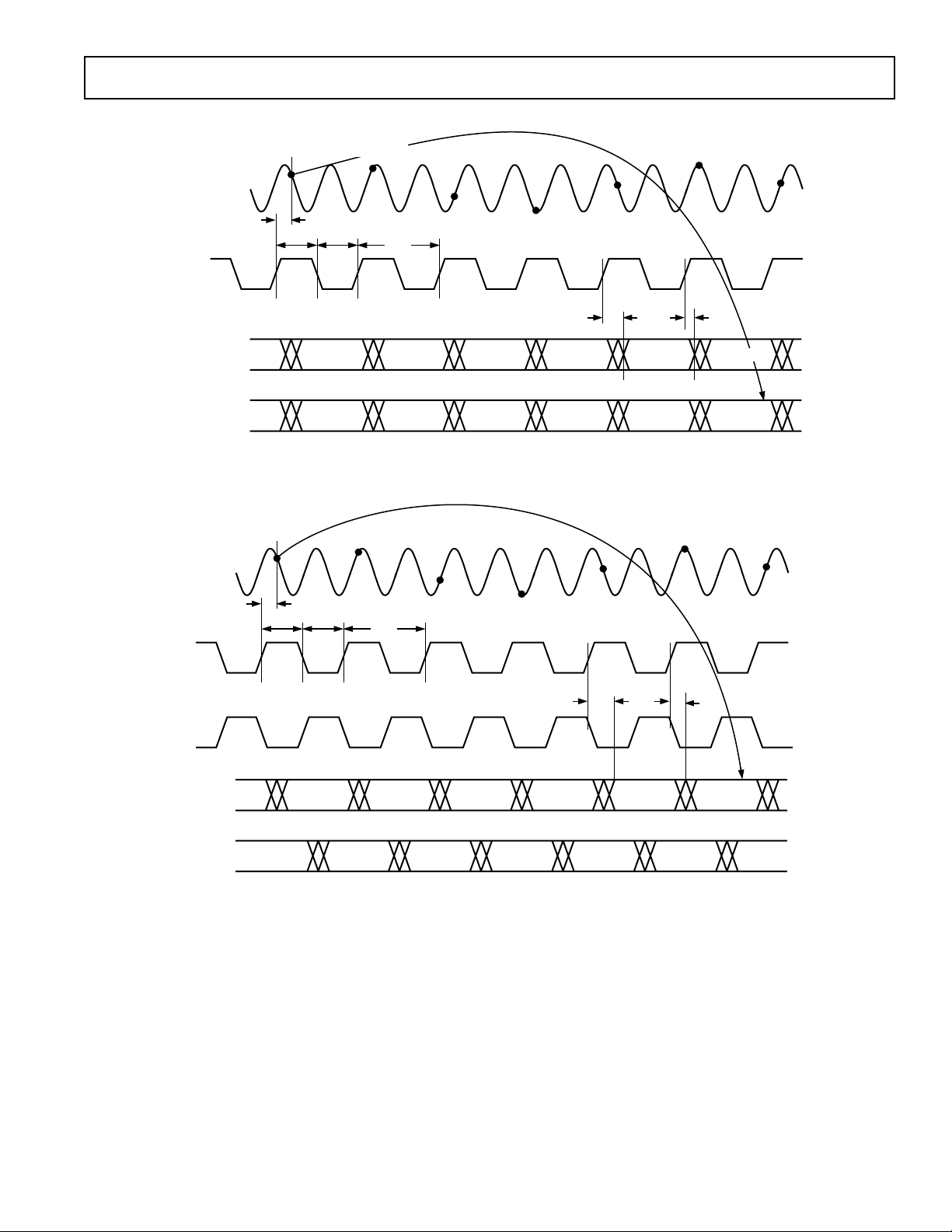
Figure 1. Normal Operation, Same Clock (S1 = 1, S2 = 0) Channel Timing
SAMPLE N SAMPLE N+1
SAMPLE N+5
DATA N+1
ENCODE A
ENCODE B
D7
–D0
A
D7
–D0
B
t
A
A
B
t
t
EL
EH
DATA N–4 DATA N–3 DATA N–2 DATA N–1 DATA N
DATA N–4 DATA N–3 DATA N–2 DATA N–1 DATA N DATA N+1
SAMPLE N+2 SAMPLE N+3 SAMPLE N+4
1/
f
S
t
PD
t
V
DATA N+1
Figure 2. Normal Operation with Two Clock Sources (S1 = 1, S2 = 0) Channel Timing
REV. 0
–5–
 Loading...